EP3179514A1 - Transistor device with reduced hot carrier injection effect - Google Patents
Transistor device with reduced hot carrier injection effect Download PDFInfo
- Publication number
- EP3179514A1 EP3179514A1 EP15199618.8A EP15199618A EP3179514A1 EP 3179514 A1 EP3179514 A1 EP 3179514A1 EP 15199618 A EP15199618 A EP 15199618A EP 3179514 A1 EP3179514 A1 EP 3179514A1
- Authority
- EP
- European Patent Office
- Prior art keywords
- dielectric layer
- layer stack
- dielectric
- transistor device
- thickness
- Prior art date
- Legal status (The legal status is an assumption and is not a legal conclusion. Google has not performed a legal analysis and makes no representation as to the accuracy of the status listed.)
- Granted
Links
Images





Classifications
-
- H—ELECTRICITY
- H10—SEMICONDUCTOR DEVICES; ELECTRIC SOLID-STATE DEVICES NOT OTHERWISE PROVIDED FOR
- H10D—INORGANIC ELECTRIC SEMICONDUCTOR DEVICES
- H10D64/00—Electrodes of devices having potential barriers
- H10D64/60—Electrodes characterised by their materials
- H10D64/66—Electrodes having a conductor capacitively coupled to a semiconductor by an insulator, e.g. MIS electrodes
- H10D64/68—Electrodes having a conductor capacitively coupled to a semiconductor by an insulator, e.g. MIS electrodes characterised by the insulator, e.g. by the gate insulator
- H10D64/681—Electrodes having a conductor capacitively coupled to a semiconductor by an insulator, e.g. MIS electrodes characterised by the insulator, e.g. by the gate insulator having a compositional variation, e.g. multilayered
- H10D64/683—Electrodes having a conductor capacitively coupled to a semiconductor by an insulator, e.g. MIS electrodes characterised by the insulator, e.g. by the gate insulator having a compositional variation, e.g. multilayered being parallel to the channel plane
-
- H—ELECTRICITY
- H10—SEMICONDUCTOR DEVICES; ELECTRIC SOLID-STATE DEVICES NOT OTHERWISE PROVIDED FOR
- H10D—INORGANIC ELECTRIC SEMICONDUCTOR DEVICES
- H10D30/00—Field-effect transistors [FET]
- H10D30/60—Insulated-gate field-effect transistors [IGFET]
- H10D30/601—Insulated-gate field-effect transistors [IGFET] having lightly-doped drain or source extensions, e.g. LDD IGFETs or DDD IGFETs
-
- H—ELECTRICITY
- H10—SEMICONDUCTOR DEVICES; ELECTRIC SOLID-STATE DEVICES NOT OTHERWISE PROVIDED FOR
- H10D—INORGANIC ELECTRIC SEMICONDUCTOR DEVICES
- H10D62/00—Semiconductor bodies, or regions thereof, of devices having potential barriers
- H10D62/10—Shapes, relative sizes or dispositions of the regions of the semiconductor bodies; Shapes of the semiconductor bodies
- H10D62/124—Shapes, relative sizes or dispositions of the regions of semiconductor bodies or of junctions between the regions
- H10D62/125—Shapes of junctions between the regions
-
- H—ELECTRICITY
- H10—SEMICONDUCTOR DEVICES; ELECTRIC SOLID-STATE DEVICES NOT OTHERWISE PROVIDED FOR
- H10D—INORGANIC ELECTRIC SEMICONDUCTOR DEVICES
- H10D62/00—Semiconductor bodies, or regions thereof, of devices having potential barriers
- H10D62/10—Shapes, relative sizes or dispositions of the regions of the semiconductor bodies; Shapes of the semiconductor bodies
- H10D62/13—Semiconductor regions connected to electrodes carrying current to be rectified, amplified or switched, e.g. source or drain regions
- H10D62/149—Source or drain regions of field-effect devices
- H10D62/151—Source or drain regions of field-effect devices of IGFETs
-
- H—ELECTRICITY
- H10—SEMICONDUCTOR DEVICES; ELECTRIC SOLID-STATE DEVICES NOT OTHERWISE PROVIDED FOR
- H10D—INORGANIC ELECTRIC SEMICONDUCTOR DEVICES
- H10D64/00—Electrodes of devices having potential barriers
- H10D64/20—Electrodes characterised by their shapes, relative sizes or dispositions
- H10D64/27—Electrodes not carrying the current to be rectified, amplified, oscillated or switched, e.g. gates
- H10D64/311—Gate electrodes for field-effect devices
- H10D64/411—Gate electrodes for field-effect devices for FETs
- H10D64/511—Gate electrodes for field-effect devices for FETs for IGFETs
- H10D64/514—Gate electrodes for field-effect devices for FETs for IGFETs characterised by the insulating layers
- H10D64/516—Gate electrodes for field-effect devices for FETs for IGFETs characterised by the insulating layers the thicknesses being non-uniform
-
- H—ELECTRICITY
- H10—SEMICONDUCTOR DEVICES; ELECTRIC SOLID-STATE DEVICES NOT OTHERWISE PROVIDED FOR
- H10D—INORGANIC ELECTRIC SEMICONDUCTOR DEVICES
- H10D64/00—Electrodes of devices having potential barriers
- H10D64/60—Electrodes characterised by their materials
- H10D64/66—Electrodes having a conductor capacitively coupled to a semiconductor by an insulator, e.g. MIS electrodes
- H10D64/68—Electrodes having a conductor capacitively coupled to a semiconductor by an insulator, e.g. MIS electrodes characterised by the insulator, e.g. by the gate insulator
- H10D64/681—Electrodes having a conductor capacitively coupled to a semiconductor by an insulator, e.g. MIS electrodes characterised by the insulator, e.g. by the gate insulator having a compositional variation, e.g. multilayered
- H10D64/685—Electrodes having a conductor capacitively coupled to a semiconductor by an insulator, e.g. MIS electrodes characterised by the insulator, e.g. by the gate insulator having a compositional variation, e.g. multilayered being perpendicular to the channel plane
-
- H—ELECTRICITY
- H10—SEMICONDUCTOR DEVICES; ELECTRIC SOLID-STATE DEVICES NOT OTHERWISE PROVIDED FOR
- H10D—INORGANIC ELECTRIC SEMICONDUCTOR DEVICES
- H10D64/00—Electrodes of devices having potential barriers
- H10D64/60—Electrodes characterised by their materials
- H10D64/66—Electrodes having a conductor capacitively coupled to a semiconductor by an insulator, e.g. MIS electrodes
- H10D64/68—Electrodes having a conductor capacitively coupled to a semiconductor by an insulator, e.g. MIS electrodes characterised by the insulator, e.g. by the gate insulator
- H10D64/691—Electrodes having a conductor capacitively coupled to a semiconductor by an insulator, e.g. MIS electrodes characterised by the insulator, e.g. by the gate insulator comprising metallic compounds, e.g. metal oxides or metal silicates
-
- H—ELECTRICITY
- H10—SEMICONDUCTOR DEVICES; ELECTRIC SOLID-STATE DEVICES NOT OTHERWISE PROVIDED FOR
- H10D—INORGANIC ELECTRIC SEMICONDUCTOR DEVICES
- H10D64/00—Electrodes of devices having potential barriers
- H10D64/60—Electrodes characterised by their materials
- H10D64/66—Electrodes having a conductor capacitively coupled to a semiconductor by an insulator, e.g. MIS electrodes
- H10D64/68—Electrodes having a conductor capacitively coupled to a semiconductor by an insulator, e.g. MIS electrodes characterised by the insulator, e.g. by the gate insulator
- H10D64/693—Electrodes having a conductor capacitively coupled to a semiconductor by an insulator, e.g. MIS electrodes characterised by the insulator, e.g. by the gate insulator the insulator comprising nitrogen, e.g. nitrides, oxynitrides or nitrogen-doped materials
-
- H—ELECTRICITY
- H10—SEMICONDUCTOR DEVICES; ELECTRIC SOLID-STATE DEVICES NOT OTHERWISE PROVIDED FOR
- H10D—INORGANIC ELECTRIC SEMICONDUCTOR DEVICES
- H10D64/00—Electrodes of devices having potential barriers
- H10D64/60—Electrodes characterised by their materials
- H10D64/66—Electrodes having a conductor capacitively coupled to a semiconductor by an insulator, e.g. MIS electrodes
- H10D64/667—Electrodes having a conductor capacitively coupled to a semiconductor by an insulator, e.g. MIS electrodes the conductor comprising a layer of alloy material, compound material or organic material contacting the insulator, e.g. TiN workfunction layers
-
- H—ELECTRICITY
- H10—SEMICONDUCTOR DEVICES; ELECTRIC SOLID-STATE DEVICES NOT OTHERWISE PROVIDED FOR
- H10P—GENERIC PROCESSES OR APPARATUS FOR THE MANUFACTURE OR TREATMENT OF DEVICES COVERED BY CLASS H10
- H10P30/00—Ion implantation into wafers, substrates or parts of devices
- H10P30/20—Ion implantation into wafers, substrates or parts of devices into semiconductor materials, e.g. for doping
Definitions
- the present disclosure relates to the field of semiconductor devices, more specifically to the field of transistor devices such as MOS transistor devices.
- Hot carrier injection also known as Channel Hot Carrier (CHC)
- CHC Channel Hot Carrier
- Hot-carrier injection is one of the mechanisms that negatively impacts the reliability of semiconductors of solid-state devices.
- a transistor device comprising
- the respective capacitances are typically defined between the metal gate layer and the channel region.
- the capacitance of the first dielectric stack is at least 10 %, more preferable at least 20%, more preferably at least 30 %, more preferably at least 50%, more preferable at least 100%, more preferable at least 200% larger than in the second dielectric layer stack.
- the electric field in the junction area e.g. on top of the junction
- the capacitances of the first and second dielectric layer stack are determined by the dielectric constants (also known as k-values) and thicknesses of the dielectric layers in the respective stacks.
- the first dielectric layer stack comprises a first dielectric layer comprising a silicon oxide SiO2 and/or SiOxNy (including SiOx and SiNx), and has a dielectric constant k1 and a second, preferably high-k, dielectric layer having a dielectric constant k4 on the silicon oxide layer, with k4 > k1.
- a low k material or layer is a layer or material having a dielectric constant k which is lower than the dielectric constant of SiO2 (3.9), and a high k material or layer is a material or layer which has a dielectric constant k which is larger than the dielectric constant of SiO2.
- low k materials are for instance Fluorine-doped silicon dioxide (k of about 3,5), Carbon-doped silicon dioxide (k of about 3), Porous silicon dioxide (k of about 2), Porous carbon-doped silicon dioxide (k ⁇ 3), and other materials known to the skilled person.
- high k materials are for instance HfO2 (k of for instance within the range of 15 to 40), doped HfO2 (15 ⁇ k ⁇ 45), HfxSiyO2, HfxCyO2, HfxTiyO2, HfxCeyO2, HfxSnyO2, HfxGeyO2, Hfx, ZrO2 (k of about 24.7), TaO5 (k of about 27), and other materials known to the skilled person.
- the high-k materials used as the upper or second layer in the first dielectric layers stack has a k-value larger than 15.
- the second dielectric layer stack comprises a single layer being a dielectric layer having a dielectric constant k23, the thickness of which corresponds to the thickness of the first layer of the first dielectric layer stack.
- the second dielectric layer stack comprises a single layer being a dielectric layer having a dielectric constant k23, the thickness of which corresponds to the thickness of the first dielectric layer stack.
- the second dielectric layer stack comprises a single layer being a dielectric layer having a dielectric constant k23, the thickness of which is in between the thickness of the first layer of the first dielectric layer stack and the thickness of the first dielectric layer stack. It is an advantage that a larger process flexibility exists for manufacturing these devices.
- the second dielectric layer stack comprises a single layer being a dielectric layer having a dielectric constant k23, the thickness of which is larger than the thickness of the first dielectric layer stack. It is an advantage that a larger process flexibility exists for manufacturing these devices.
- k1 ⁇ k23 ⁇ k4.
- suitable materials are for instance silicon monoxide (SiO, K of about 5.0), silicon dioxide (SiO2 K of about 3.9), silicon nitride (SiO3N4 K of about 6), alkali halides (rubidium bromide, RbBr, K of about 4.7), lithium fluoride, LiF, K of about 9.2), and other materials known to the skilled person.
- the second dielectric layer stack comprises a first dielectric layer having a dielectric constant k2 and a second dielectric layer having a dielectric constant k3 on top of the first dielectric layer.
- the first dielectric layer of the second dielectric layer stack comprises silicon oxide and/or SiOxNy (including SiOx and SiNx).
- the first dielectric layer of the second dielectric layer stack comprises the same material as the material of the first layer of the first layer stack, and further comprises atoms which cause k2 ⁇ k1.
- These embodiments may be the result of a process wherein a single first layer is provided, common for the first and second dielectric layer stack, and whereby the layer is implanted with atoms/ions, resulting in a lowering of the dielectric constant in the implanted region.
- a diffusion process can be used, resulting in a similar structure. It is an advantage that the production process for devices of this embodiment is simplified as a single layer is forming the first layer of the first and second dielectric layer stack.
- the first dielectric layer of the second dielectric layer stack has a thickness equal to the first layer of the first dielectric layer stack
- the second dielectric layer of the second dielectric layer stack has a thickness which is smaller or equal than the thickness of the high-k layer of the first dielectric layer stack.
- the second dielectric layer stack is provided laterally adjacent and in physical contact with the first dielectric layer stack, on both sides of the first dielectric layer stack.
- top, bottom, over, under and the like in the description and the claims are used for descriptive purposes and not necessarily for describing relative positions. The terms so used are interchangeable under appropriate circumstances and the embodiments of the disclosure described herein can operate in other orientations than described or illustrated herein.
- Figure 1 illustrates a state of the art MOS transistor device.
- a channel region C is defined, which is delimited by a source S and a drain D region, forming respective junctions 11 and 12 therewith.
- a gate dielectric layer stack is provided, e.g. a silicon oxide (SiO2) layer 2 and a high-k dielectric layer 3 on top of the silicon oxide layer 2.
- a metal gate layer 4 and poly-silicon layer 5 is provided on top of the dielectric layer stack.
- the gate stack is laterally defined by spacer structures 6.
- Figure 2 illustrates a transistor device according to a first embodiment of the present disclosure.
- a channel region C is defined, which is delimited by a source S and a drain D region, forming respective junctions 11 and 12 therewith.
- the MOS transistor device comprises
- the first dielectric layer stack comprises a first layer 2 comprising a silicon oxide SiO2 and/or SiOx and/or SiON, and has a dielectric constant k1 and a second, high-k dielectric layer 3 having a dielectric constant k4 on said silicon oxide layer 2, with k4 > k1.
- the second dielectric layer stack comprises a single layer 20 being a dielectric layer having a dielectric constant k23.
- the thickness of the single dielectric layer 20, and thus of the second dielectric layer stack is about equal or equal to the thickness of the first layer 2 of the first dielectric layer stack.
- the metal gate layer 4 is provided on both the first and the second dielectric layer stacks.
- the skilled person will recognize that fulfilling the boundary condition that the capacitance of the first dielectric layer stack is larger than the capacitance of the second dielectric layer stack, is a matter of choosing the thicknesses and k-values of the dielectric layers in the respective stacks.
- Figure 3 illustrates a transistor device according to a second embodiment of the present disclosure.
- the second embodiment is similar as the first embodiment, and differs there from only in the fact that the thickness of the second dielectric stack, embodied by a single dielectric layer 20, is in between the thickness of the first layer 2 of the first dielectric layer stack and the thickness of the first dielectric layer stack. This provides a better leakage current control than in the embodiment described in relation with Fig. 2 .
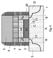
- Figure 4 illustrates a transistor device according to a third embodiment of the present disclosure.
- the third embodiment is similar as the first and second embodiment, and differs there from only in the fact that the thickness of the second dielectric stack, embodied by a single dielectric layer 20, is equal of about equal to the thickness of the first dielectric layer stack 2,3. It is an advantage over the embodiments described in relation to Fig. 2 and Fig. 3 that when manufacturing the device, an optimal control of Metal Gate deposition exist, as there is less or no potential non-uniformity related to the Metal Gate fabrication itself.
- Figure 5 illustrates a transistor device according to a fourth embodiment of the present disclosure.
- the fourth embodiment is similar as the first, second and third embodiment, and differs there from only in the fact that the thickness of the second dielectric stack, embodied by a single dielectric layer 20, is larger than the thickness of the first dielectric layer stack. This has the advantage over the previous embodiments that the electric field can further be reduced, and that a larger manufacturing flexibility is available.
- Figure 6 illustrates a transistor device according to a fifth embodiment of the present disclosure, an embodiment of a second type.
- the embodiment is similar as the embodiments described before, of the first type, but differs there from in that the second dielectric layer stack comprises a first dielectric layer 20 on the main surface 13, and a second dielectric layer 21 on top of the first dielectric layer 20.
- the first dielectric layer 20 and the second dielectric layer 21 have a thickness which is equal or about equal to the thicknesses of the first and second dielectric layers 2,3 of the first dielectric layer stack. This may be advantageous as it may simplify the production process of the transistor device.
- the thicknesses of the first layer 20 and/or of the second layer 21 of the second dielectric layer stack can be different from the respective first layer 2 and second layer 3 of the first dielectric layer stack 2,3.
- the (i.e. combined) thickness of the second dielectric layer stack can be equal, about equal, smaller, or larger than the thickness of the first dielectric layer stack 2,3.
- the first dielectric layer stack can thus for instance comprise a first layer 2 comprising a silicon oxide SiO2 and/or SiOxNy (including SiOx and SiNx), and has a dielectric constant k1 and a second, high-k dielectric layer 3 having a dielectric constant k4 on said silicon oxide layer 2, with k4 > k1.
- a first layer 2 comprising a silicon oxide SiO2 and/or SiOxNy (including SiOx and SiNx)
- the first layer of the second dielectric layer stack comprises the same material as the first layer of the first dielectric layer stack, and is thus equally thick; they can for instance be formed in a single, common process step.
- the layer can be modified in the second area, e.g. by implantation or in-diffusion of atoms (e.g. F-atoms), which reduces the k-value of the layer locally.
- Figure 8 illustrates a transistor device according to a seventh embodiment of the present disclosure. This embodiment is similar to the embodiment described in relation with Fig. 6 and Fig. 7 .
- the second layer 21 of the second dielectric layer stack is thinner than the second layer of the first dielectric layer stack 3.
- the second dielectric layer stack is thus thinner than the first dielectric layer stack.
- the metal gate layer 4 is provided on the first dielectric layer stack 2,3 and the second dielectric layer stack 20, 21.
- the dielectric constants of the respective dielectric layers are preferably following any of the following relations, or any consistent combination thereof:
- the above embodiments can be applied on at least one side of the channel region C i.e. in the area B above the drain junction 13 or in the area B above the source junction 12.
- any of the disclosed embodiments can be applied on the source junction 12 and any of the disclosed embodiments can be applied on the drain junction 13, wherein the second dielectric layer stack can be different above the source junction 12 and the drain junction 13.
- the same second dielectric layer stack is provided laterally adjacent and in physical contact with the first dielectric layer stack 2,3 , on both sides of the first dielectric layer stack, as illustrated in the different embodiments.
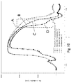
- Figures 9 to 11 show simulation results indicating the effectiveness of the embodiments of the present disclosure.
- Fig 9 represents simulation results for an embodiment described in relation with Fig. 6 .
- the results are believed to be similar for any of the other embodiments.
- the graph on the right shows the 2D plot of same quantity, but for embodiments of the present disclosure. It is visible that in the region underneath the different dielectric constant (k2), the electric field is modified and reduced, in particular on the drain side.
- Fig 11 shows the carrier temperature, in the same case of before, simulated with a hydrodynamic transport model. It is clear that a reduction of the temperature is observed, when the proposed solution according to embodiments of the present disclosure is used. This is particularly observed below the region with lower dielectric constant (circles: prior art; crosses: embodiments of the present disclosure). Such a temperature is directly related to the generation of hot carriers, responsible for the induced damage which is required to be reduced.
Landscapes
- Insulated Gate Type Field-Effect Transistor (AREA)
- Thin Film Transistor (AREA)
Abstract
a. a channel region in a substrate partially delimited by a source and a drain junction at a main surface of the substrate;
b. a first dielectric layer stack arranged on the channel region on the main surface of the substrate, the orthogonal projection of the first dielectric layer stack on the main surface being in between and not covering the junctions and defining a first area;
c. a second dielectric layer stack laterally adjacent to and in contact with the first dielectric layer stack, the orthogonal projection of the second dielectric layer stack on the main surface comprising the junction and defining a second area;
d. a metal gate layer on top of the first and the second dielectric layer stack, the orthogonal projection of the metal gate layer on the main surface covering at least the first area and the second area;
wherein the capacitance of the first dielectric layer stack is larger than the capacitance of the second dielectric layer stack.
Description
- The present disclosure relates to the field of semiconductor devices, more specifically to the field of transistor devices such as MOS transistor devices.
- Hot carrier injection (HCl), also known as Channel Hot Carrier (CHC), is a phenomenon known in solid-state electronic devices wherein an electron or a "hole" gains sufficient kinetic energy to overcome a potential barrier necessary to break an interface state. In the field of MOS transistors, charge carriers can get trapped in the gate dielectric of the transistor, which can change the switching characteristics of the transistor permanently. Hot-carrier injection is one of the mechanisms that negatively impacts the reliability of semiconductors of solid-state devices.
- This phenomena is well known by decades, as well as some proposed solutions, and it is mitigated by specific process solutions (e.g. smoothening of the junction profile by doping adjustment) and design solutions (e.g. reduction of applied field seen by devices, according to Safe Operating Conditions).
- There exists a need in industry for novel transistor devices with reduced CHC effects.
- It is an aim of the present disclosure to provide a transistor device, e.g. a MOS transistor device, with reduced hot carrier injection effect.
- This aim is achieved according to the disclosure with the transistor device showing the technical characteristics of the first independent claim.
- In embodiments according to the present disclosure, a transistor device is disclosed comprising
- a. a channel region in a substrate partially delimited by a source and a drain junction at a main surface of the substrate;
- b. a first dielectric layer stack arranged on the channel region on the main surface of the substrate, the orthogonal projection of the first dielectric layer stack on the main surface being in between and not covering the junctions and defining a first area;
- c. a second dielectric layer stack laterally adjacent to and in physical contact with the first dielectric layer stack, the orthogonal projection of the second dielectric layer stack on the main surface comprising the junction and defining a second area;
- d. a metal gate layer on top of the first and the second dielectric layer stack, the orthogonal projection of the metal gate layer on the main surface covering at least the first area and the second area;
- wherein the capacitance of the first dielectric layer stack is larger than the capacitance of the second dielectric layer stack.
- The respective capacitances are typically defined between the metal gate layer and the channel region.
- According to preferred embodiments, the capacitance of the first dielectric stack is at least 10 %, more preferable at least 20%, more preferably at least 30 %, more preferably at least 50%, more preferable at least 100%, more preferable at least 200% larger than in the second dielectric layer stack.
- It is an advantage embodiments of the present disclosure that the electric field in the junction area, e.g. on top of the junction, can be reduced, reducing the occurrence of HCl, while at the same time maintaining good channel control from the gate. It is believed that the best trade-off between potential increase in gate leakage, possible detrimental reduction in performance and reduction of the coupling on top of the overlap region can be achieved.
- The skilled person will recognize that the capacitances of the first and second dielectric layer stack (here present in between a common gate metal layer and a common channel region) are determined by the dielectric constants (also known as k-values) and thicknesses of the dielectric layers in the respective stacks. Below, various embodiments of the present disclosure are described.
- According to preferred embodiments, the first dielectric layer stack comprises a first dielectric layer comprising a silicon oxide SiO2 and/or SiOxNy (including SiOx and SiNx), and has a dielectric constant k1 and a second, preferably high-k, dielectric layer having a dielectric constant k4 on the silicon oxide layer, with k4 > k1.
- In the art, a low k material or layer is a layer or material having a dielectric constant k which is lower than the dielectric constant of SiO2 (3.9), and a high k material or layer is a material or layer which has a dielectric constant k which is larger than the dielectric constant of SiO2.
- Examples of low k materials are for instance Fluorine-doped silicon dioxide (k of about 3,5), Carbon-doped silicon dioxide (k of about 3), Porous silicon dioxide (k of about 2), Porous carbon-doped silicon dioxide (k < 3), and other materials known to the skilled person.
- Examples of high k materials are for instance HfO2 (k of for instance within the range of 15 to 40), doped HfO2 (15<k<45), HfxSiyO2, HfxCyO2, HfxTiyO2, HfxCeyO2, HfxSnyO2, HfxGeyO2, Hfx, ZrO2 (k of about 24.7), TaO5 (k of about 27), and other materials known to the skilled person. According to preferred embodiments, the high-k materials used as the upper or second layer in the first dielectric layers stack has a k-value larger than 15.
- According to preferred embodiments of a first type, the second dielectric layer stack comprises a single layer being a dielectric layer having a dielectric constant k23, the thickness of which corresponds to the thickness of the first layer of the first dielectric layer stack.
- According to preferred embodiments of a first type, the second dielectric layer stack comprises a single layer being a dielectric layer having a dielectric constant k23, the thickness of which corresponds to the thickness of the first dielectric layer stack.
- According to preferred embodiments of a first type, the second dielectric layer stack comprises a single layer being a dielectric layer having a dielectric constant k23, the thickness of which is in between the thickness of the first layer of the first dielectric layer stack and the thickness of the first dielectric layer stack. It is an advantage that a larger process flexibility exists for manufacturing these devices.
- According to preferred embodiments of a first type, the second dielectric layer stack comprises a single layer being a dielectric layer having a dielectric constant k23, the thickness of which is larger than the thickness of the first dielectric layer stack. It is an advantage that a larger process flexibility exists for manufacturing these devices.
- According to preferred embodiments, k1<=k23<k4.
- For instance, with k1=k(SiO2) < k23 < k4=k(HfO2), suitable materials (having intermediate k value in between k1 and k4) are for instance silicon monoxide (SiO, K of about 5.0), silicon dioxide (SiO2 K of about 3.9), silicon nitride (SiO3N4 K of about 6), alkali halides (rubidium bromide, RbBr, K of about 4.7), lithium fluoride, LiF, K of about 9.2), and other materials known to the skilled person.
- It is an advantage of embodiments having single dielectric layer in the second dielectric layer stack is more easy to manufacture, as compared to embodiment of the second type described below.
- According to preferred embodiments of a second type, the second dielectric layer stack comprises a first dielectric layer having a dielectric constant k2 and a second dielectric layer having a dielectric constant k3 on top of the first dielectric layer.
- According to preferred embodiments of a second type, k2<k3.
- According to preferred embodiments of a second type, k1>k2, and k2<k3<k4.
- According to alternative preferred embodiments of a second type, k1<k2<k3<k4.
- According to still alternative preferred embodiments of a second type, k1<k3<k2<k4. According to preferred embodiments of a second type, the first dielectric layer of the second dielectric layer stack comprises silicon oxide and/or SiOxNy (including SiOx and SiNx).
- According to preferred embodiments of a second type, the first dielectric layer of the second dielectric layer stack comprises the same material as the material of the first layer of the first layer stack, and further comprises atoms which cause k2<k1. These embodiments may be the result of a process wherein a single first layer is provided, common for the first and second dielectric layer stack, and whereby the layer is implanted with atoms/ions, resulting in a lowering of the dielectric constant in the implanted region. Instead of implantation, also a diffusion process can be used, resulting in a similar structure. It is an advantage that the production process for devices of this embodiment is simplified as a single layer is forming the first layer of the first and second dielectric layer stack.
- According to preferred embodiments of a second type, the first dielectric layer of the second dielectric layer stack has a thickness equal to the first layer of the first dielectric layer stack, and the second dielectric layer of the second dielectric layer stack has a thickness which is smaller or equal than the thickness of the high-k layer of the first dielectric layer stack.
- According to preferred embodiments of a second type, the second dielectric layer stack is provided laterally adjacent and in physical contact with the first dielectric layer stack, on both sides of the first dielectric layer stack.
- Features and advantages disclosed for one of the above aspects of the present disclosure are hereby also implicitly disclosed for the other aspects, mutatis mutandis, as the skilled person will recognize.
- Certain objects and advantages of various inventive aspects have been described herein above. It is understood that this summary is merely an example and is not intended to limit the scope of the disclosure. The disclosure, both as to organization and method of operation, together with features and advantages thereof, may best be understood by reference to the following detailed description when read in conjunction with the accompanying drawings.
- The disclosure will be further elucidated by means of the following description and the appended figures.
-
Figure 1 illustrates a state of the art MOS transistor device. -
Figures 2 to 8 illustrate transistor devices according to a first to seventh embodiment of the present disclosure. -
Figures 9 to 11 show simulation results indicating the effectiveness of embodiments of the present disclosure. - The present disclosure will be described with respect to particular embodiments and with reference to certain drawings but the disclosure is not limited thereto but only by the claims. The drawings described are only schematic and are non-limiting. In the drawings, the size of some of the elements may be exaggerated and not drawn on scale for illustrative purposes. The dimensions and the relative dimensions do not necessarily correspond to actual reductions to practice of the disclosure.
- Furthermore, the terms first, second, third and the like in the description and in the claims, are used for distinguishing between similar elements and not necessarily for describing a sequential or chronological order. The terms are interchangeable under appropriate circumstances and the embodiments of the disclosure can operate in other sequences than described or illustrated herein.
- Moreover, the terms top, bottom, over, under and the like in the description and the claims are used for descriptive purposes and not necessarily for describing relative positions. The terms so used are interchangeable under appropriate circumstances and the embodiments of the disclosure described herein can operate in other orientations than described or illustrated herein.
- Furthermore, the various embodiments, although referred to as "preferred" are to be construed as example manners in which the disclosure may be implemented rather than as limiting the scope of the disclosure.
-
Figure 1 illustrates a state of the art MOS transistor device. In asilicon substrate 1, a channel region C is defined, which is delimited by a source S and a drain D region, formingrespective junctions 11 and 12 therewith. On top of the channel C, on amain surface 13 of thesubstrate 1, a gate dielectric layer stack is provided, e.g. a silicon oxide (SiO2)layer 2 and a high-k dielectric layer 3 on top of thesilicon oxide layer 2. On top of the dielectric layer stack, ametal gate layer 4 and poly-silicon layer 5 is provided. The gate stack is laterally defined byspacer structures 6. These state of the art MOS transistor devices often suffer from the HCl effect. -
Figure 2 illustrates a transistor device according to a first embodiment of the present disclosure. In asilicon substrate 1, a channel region C is defined, which is delimited by a source S and a drain D region, formingrespective junctions 11 and 12 therewith. - The MOS transistor device comprises
- a. a channel region C in a
substrate 1 partially delimited by asource junction 12 and a drain junction 11 at a main surface 13 (the upper surface) of thesubstrate 1; - b. a first dielectric layer stack arranged on the channel region C on the
main surface 13 of thesubstrate 1, the orthogonal projection of the first dielectric layer stack on themain surface 13 being in between and not covering thejunctions 11, 12 and defining a first area A; - c. a second dielectric layer stack laterally adjacent to and in physical contact with the first dielectric layer stack, the orthogonal projection of the second dielectric layer stack on the
main surface 13 comprising thejunction 11, 12 and defining a second area B; - d. a
metal gate layer 4 on top of the first and the second dielectric layer stack, the orthogonal projection of themetal gate layer 4 on the main surface covering at least the first area A and the second area B;- wherein the capacitance of the first dielectric layer stack is larger than the capacitance of the second dielectric layer stack.
- In the embodiment depicted in
Fig. 2 , but also in the further embodiments which will be described in relation withFig. 3 to Fig. 8 , the first dielectric layer stack comprises afirst layer 2 comprising a silicon oxide SiO2 and/or SiOx and/or SiON, and has a dielectric constant k1 and a second, high-k dielectric layer 3 having a dielectric constant k4 on saidsilicon oxide layer 2, with k4 > k1. - The second dielectric layer stack comprises a
single layer 20 being a dielectric layer having a dielectric constant k23. The thickness of thesingle dielectric layer 20, and thus of the second dielectric layer stack, is about equal or equal to the thickness of thefirst layer 2 of the first dielectric layer stack. Themetal gate layer 4 is provided on both the first and the second dielectric layer stacks. - An example of typical fabrication parameters are the following (ranges are indicative and not limiting):
- SiO2 thickness (common to all the cases): preferred value between 0.5nm to 2.0 nm in a low voltage applications; or between 2 nm and 5nm for I/O oriented applications(VDD~2.75-3V); or larger than 5 nm for VDD>=3V;
- High-k thickness: preferred value of about2nm; thickness preferably between 1.5nm and 5 nm; preferred high-k material is (e.g. doped) HfO2;
- Metal Gate: preferred materials :TiN, TaN, TiAlN; having a typical thickness in between (about) 2 to(about) 10 nm;
- Spacers thickness: preferable larger than 5nm; typical values of the spaced thickness are values between 5 and 20 nm for Low Voltage cases; or between 20 and 40 nm for higher voltage cases (i.e.: VDD>2.75V);
- Lateral dimension of the second area , on top of the junction, preferably within the range of 5 to 10 nm, preferably about ¼ or ¼ of the gate length, preferably a function of the gate length;
- Lateral dimension of the first area: depending on the technology nodes, down to 15-20 nm for advanced ultrascaled technology (VD<1V) up to longer case (Lgate larger than 50nm, and smaller than 200 nm, or smaller than 1um, or smaller than 10um) ;
- Poly-silicon layer of the gate stack: preferably having a thickness larger than 50 nm. (Alternatively, the gate stack can comprise a filling Metal material (e.g. W) instead of a poly-silicon layer.
- For any of the described embodiments, the skilled person will recognize that fulfilling the boundary condition that the capacitance of the first dielectric layer stack is larger than the capacitance of the second dielectric layer stack, is a matter of choosing the thicknesses and k-values of the dielectric layers in the respective stacks.
-
Figure 3 illustrates a transistor device according to a second embodiment of the present disclosure. The second embodiment is similar as the first embodiment, and differs there from only in the fact that the thickness of the second dielectric stack, embodied by asingle dielectric layer 20, is in between the thickness of thefirst layer 2 of the first dielectric layer stack and the thickness of the first dielectric layer stack. This provides a better leakage current control than in the embodiment described in relation withFig. 2 . -
Figure 4 illustrates a transistor device according to a third embodiment of the present disclosure. The third embodiment is similar as the first and second embodiment, and differs there from only in the fact that the thickness of the second dielectric stack, embodied by asingle dielectric layer 20, is equal of about equal to the thickness of the firstdielectric layer stack Fig. 2 andFig. 3 that when manufacturing the device, an optimal control of Metal Gate deposition exist, as there is less or no potential non-uniformity related to the Metal Gate fabrication itself. -
Figure 5 illustrates a transistor device according to a fourth embodiment of the present disclosure. The fourth embodiment is similar as the first, second and third embodiment, and differs there from only in the fact that the thickness of the second dielectric stack, embodied by asingle dielectric layer 20, is larger than the thickness of the first dielectric layer stack. This has the advantage over the previous embodiments that the electric field can further be reduced, and that a larger manufacturing flexibility is available. - In all of the embodiments disclosed in relation with
Fig. 2 to Fig. 5 , the following relation is preferably applicable for the dielectric constants; k1<=k23<k4. -
Figure 6 illustrates a transistor device according to a fifth embodiment of the present disclosure, an embodiment of a second type. The embodiment is similar as the embodiments described before, of the first type, but differs there from in that the second dielectric layer stack comprises afirst dielectric layer 20 on themain surface 13, and asecond dielectric layer 21 on top of thefirst dielectric layer 20. In the embodiment depicted, thefirst dielectric layer 20 and thesecond dielectric layer 21 have a thickness which is equal or about equal to the thicknesses of the first and seconddielectric layers first layer 20 and/or of thesecond layer 21 of the second dielectric layer stack can be different from the respectivefirst layer 2 andsecond layer 3 of the firstdielectric layer stack dielectric layer stack
The first dielectric layer stack can thus for instance comprise afirst layer 2 comprising a silicon oxide SiO2 and/or SiOxNy (including SiOx and SiNx), and has a dielectric constant k1 and a second, high-k dielectric layer 3 having a dielectric constant k4 on saidsilicon oxide layer 2, with k4 > k1. In preferred embodiments, illustrated inFig. 7 , the first layer of the second dielectric layer stack comprises the same material as the first layer of the first dielectric layer stack, and is thus equally thick; they can for instance be formed in a single, common process step. In the second area the layer can be modified in the second area, e.g. by implantation or in-diffusion of atoms (e.g. F-atoms), which reduces the k-value of the layer locally. -
Figure 8 illustrates a transistor device according to a seventh embodiment of the present disclosure. This embodiment is similar to the embodiment described in relation withFig. 6 andFig. 7 . Thefirst layer 20 of the second dielectric layer stack is here the same as thefirst layer 2 of the first dielectric layer stack; for instance it can be formed in a single step, such that k1 = k2. Thesecond layer 21 of the second dielectric layer stack is thinner than the second layer of the firstdielectric layer stack 3. The second dielectric layer stack is thus thinner than the first dielectric layer stack. Themetal gate layer 4 is provided on the firstdielectric layer stack dielectric layer stack - In all of the embodiments described above of the second type, the dielectric constants of the respective dielectric layers are preferably following any of the following relations, or any consistent combination thereof:
- k1>=k2, and k2<k3<k4;
- k1<k2<k3<k4;
- k1<k3<k2<k4;
- k2<k3;
- k2>k3;
- k3<k1 (or k3<3.9 in case that the first dielectric layer of the first dielectric layer stack comprises SiO2).
- It is noted that in principle, the above embodiments, as well as the general concepts of the present disclosure, can be applied on at least one side of the channel region C i.e. in the area B above the
drain junction 13 or in the area B above thesource junction 12. In principle, any of the disclosed embodiments can be applied on thesource junction 12 and any of the disclosed embodiments can be applied on thedrain junction 13, wherein the second dielectric layer stack can be different above thesource junction 12 and thedrain junction 13. Preferably, the same second dielectric layer stack is provided laterally adjacent and in physical contact with the firstdielectric layer stack -
Figures 9 to 11 show simulation results indicating the effectiveness of the embodiments of the present disclosure. - An example of the effectiveness of the proposed solution according to embodiments of the present disclosure is shown in
Fig 9 , which represents simulation results for an embodiment described in relation withFig. 6 . The results are believed to be similar for any of the other embodiments. - The left side shows the 2D graph with the Abs(Efield), absolute value of the electric field components SORT[ (E_X^2 + E_Y^2) ], which includes the effect of both components of the electric field (horizontal and vertical), when the transistor is switched on (e.g.: Vs=0V, VG>0V, 0<VD<VDD for an NMOS case). In this case, the Equivalent Oxide thickness was 5 nm and the conditions were Vg=1.5V, Vd=1 V .
- The graph on the right shows the 2D plot of same quantity, but for embodiments of the present disclosure. It is visible that in the region underneath the different dielectric constant (k2), the electric field is modified and reduced, in particular on the drain side.
- Such an effect is evidenced also in
Fig 10 , where the 1 D plot of the Abs(Efield) along the channel direction (from Source to Drain) is shown. Comparing the state of the art solution with the embodiments of the present disclosure, it is clear that a reduction in the Efield is observed below the region with lower dielectric constant. This example shows the reduction of the Absolute value of the electric field (A : prior art; C : embodiments of the present disclosure), as well as one of for the Vertical Component (Y-component) of the Electric Field (B: prior art; D: embodiments of the present disclosure). -
Fig 11 shows the carrier temperature, in the same case of before, simulated with a hydrodynamic transport model. It is clear that a reduction of the temperature is observed, when the proposed solution according to embodiments of the present disclosure is used. This is particularly observed below the region with lower dielectric constant (circles: prior art; crosses: embodiments of the present disclosure). Such a temperature is directly related to the generation of hot carriers, responsible for the induced damage which is required to be reduced. - The foregoing description details certain embodiments of the disclosure. It will be appreciated, however, that no matter how detailed the foregoing appears in text, the disclosure may be practiced in many ways.
- While the above detailed description has shown, described, and pointed out novel features of the invention as applied to various embodiments, it will be understood that various omissions, substitutions, and changes in the form and details of the device or process illustrated may be made by those skilled in the technology without departing from the disclosure.
Claims (15)
- A transistor device comprisinga. a channel region in a substrate partially delimited by a source and a drain junction at a main surface of said substrate;b. a first dielectric layer stack arranged on said channel region on said main surface of said substrate, the orthogonal projection of said first dielectric layer stack on said main surface being in between and not covering said junctions and defining a first area;c. a second dielectric layer stack laterally adjacent to and in contact with said first dielectric layer stack, the orthogonal projection of said second dielectric layer stack on said main surface comprising said junction and defining a second area;d. a metal gate layer on top of said first and said second dielectric layer stack, the orthogonal projection of said metal gate layer on said main surface covering at least said first area and said second area;wherein the capacitance of the first dielectric layer stack is larger than the capacitance of the second dielectric layer stack.
- A transistor device according to claim 1, wherein said first dielectric layer stack comprises a first layer comprising a silicon oxide SiO2 and/or SiOxNy, and has a dielectric constant k1 and a second, high-k dielectric layer having a dielectric constant k4 on said silicon oxide layer, with k4 > k1.
- A transistor device according to claim 2, wherein said second dielectric layer stack comprises a single layer being a dielectric layer having a dielectric constant k23, the thickness of which corresponds to the thickness of the first layer of the first dielectric layer stack.
- A transistor device according to claim 2, wherein said second dielectric layer stack comprises a single layer being a dielectric layer having a dielectric constant k23, the thickness of which corresponds to the thickness of the first dielectric layer stack.
- A transistor device according to claim 2, wherein said second dielectric layer stack comprises a single layer being a dielectric layer having a dielectric constant k23, the thickness of which is larger than the thickness of the first dielectric layer stack.
- A transistor device according to claim 2, wherein said second dielectric layer stack comprises a single layer being a dielectric layer having a dielectric constant k23, the thickness of which is in between the thickness of the first layer of the first dielectric layer stack and the thickness of the first dielectric layer stack.
- A transistor device according to any of claims 3 to 6, wherein k1 <=k23<k4.
- A transistor device according to claim 2, wherein said second dielectric layer stack comprises a first dielectric layer having a dielectric constant k2 and a second dielectric layer having a dielectric constant k3 on top of said first dielectric layer.
- A transistor device according to claim 8, wherein k1>k2, and k2<k3<k4.
- A transistor device according to claim 8, wherein k1<k2<k3<k4.
- A transistor device according to claim 8, wherein k1<k3<k2<k4.
- A transistor device according to any of claim 8 to 11, wherein the first dielectric layer of the second dielectric layer stack comprises silicon oxide and/or SiOxNy.
- A transistor device according to claim 8 or 9, wherein the first dielectric layer of the second dielectric layer stack comprises the same material as the material of the first layer of the first layer stack, and further comprises atoms which cause k2<k1.
- A transistor device according to claim any of claims 8 to 13, wherein the first dielectric layer of the second dielectric layer stack has a thickness equal to the first layer of the first dielectric layer stack, and wherein the second dielectric layer of the second dielectric layer stack has a thickness which is smaller or equal than the thickness of the high-k layer of the first dielectric layer stack.
- A transistor according to any of the previous claims, wherein said second dielectric layer stack is provided laterally adjacent and in physical contact with said first dielectric layer stack, on both sides of said first dielectric layer stack.
Priority Applications (2)
| Application Number | Priority Date | Filing Date | Title |
|---|---|---|---|
| EP15199618.8A EP3179514B1 (en) | 2015-12-11 | 2015-12-11 | Transistor device with reduced hot carrier injection effect |
| US15/374,886 US10439036B2 (en) | 2015-12-11 | 2016-12-09 | Transistor device with reduced hot carrier injection effect |
Applications Claiming Priority (1)
| Application Number | Priority Date | Filing Date | Title |
|---|---|---|---|
| EP15199618.8A EP3179514B1 (en) | 2015-12-11 | 2015-12-11 | Transistor device with reduced hot carrier injection effect |
Publications (2)
| Publication Number | Publication Date |
|---|---|
| EP3179514A1 true EP3179514A1 (en) | 2017-06-14 |
| EP3179514B1 EP3179514B1 (en) | 2024-01-24 |
Family
ID=55024768
Family Applications (1)
| Application Number | Title | Priority Date | Filing Date |
|---|---|---|---|
| EP15199618.8A Active EP3179514B1 (en) | 2015-12-11 | 2015-12-11 | Transistor device with reduced hot carrier injection effect |
Country Status (2)
| Country | Link |
|---|---|
| US (1) | US10439036B2 (en) |
| EP (1) | EP3179514B1 (en) |
Families Citing this family (1)
| Publication number | Priority date | Publication date | Assignee | Title |
|---|---|---|---|---|
| EP3339244A1 (en) * | 2016-12-21 | 2018-06-27 | IMEC vzw | Source and drain contacts in fin- or nanowire- based semiconductor devices. |
Citations (6)
| Publication number | Priority date | Publication date | Assignee | Title |
|---|---|---|---|---|
| JPH113990A (en) * | 1996-04-22 | 1999-01-06 | Sony Corp | Semiconductor device and manufacturing method thereof |
| WO2000049643A2 (en) * | 1999-02-16 | 2000-08-24 | Koninklijke Philips Electronics N.V. | Gate insulator comprising high and low dielectric constant parts |
| US20020142529A1 (en) * | 2001-03-29 | 2002-10-03 | Satoshi Matsuda | Semiconductor device comprising buried channel region and method for manufacturing the same |
| US20070018238A1 (en) * | 2005-07-06 | 2007-01-25 | Kabushiki Kaisha Toshiba | Semiconductor device |
| US20120205751A1 (en) * | 2011-02-14 | 2012-08-16 | Kabushiki Kaisha Toshiba | Semiconductor device |
| US20150123167A1 (en) * | 2013-11-04 | 2015-05-07 | SK Hynix Inc. | Method and gate structure for threshold voltage modulation in transistors |
Family Cites Families (6)
| Publication number | Priority date | Publication date | Assignee | Title |
|---|---|---|---|---|
| US5960270A (en) * | 1997-08-11 | 1999-09-28 | Motorola, Inc. | Method for forming an MOS transistor having a metallic gate electrode that is formed after the formation of self-aligned source and drain regions |
| US6436774B1 (en) * | 2001-01-26 | 2002-08-20 | Chartered Semiconductor Manufacturing Ltd. | Method for forming variable-K gate dielectric |
| US6406945B1 (en) | 2001-01-26 | 2002-06-18 | Chartered Semiconductor Manufacturing Ltd. | Method for forming a transistor gate dielectric with high-K and low-K regions |
| US7161203B2 (en) * | 2004-06-04 | 2007-01-09 | Micron Technology, Inc. | Gated field effect device comprising gate dielectric having different K regions |
| JP2014204041A (en) * | 2013-04-08 | 2014-10-27 | ルネサスエレクトロニクス株式会社 | Semiconductor device manufacturing method |
| KR20150121399A (en) * | 2014-04-18 | 2015-10-29 | 에스케이하이닉스 주식회사 | Non-volatile memory device having charge trapping layer and method of fabricating the same |
-
2015
- 2015-12-11 EP EP15199618.8A patent/EP3179514B1/en active Active
-
2016
- 2016-12-09 US US15/374,886 patent/US10439036B2/en active Active
Patent Citations (6)
| Publication number | Priority date | Publication date | Assignee | Title |
|---|---|---|---|---|
| JPH113990A (en) * | 1996-04-22 | 1999-01-06 | Sony Corp | Semiconductor device and manufacturing method thereof |
| WO2000049643A2 (en) * | 1999-02-16 | 2000-08-24 | Koninklijke Philips Electronics N.V. | Gate insulator comprising high and low dielectric constant parts |
| US20020142529A1 (en) * | 2001-03-29 | 2002-10-03 | Satoshi Matsuda | Semiconductor device comprising buried channel region and method for manufacturing the same |
| US20070018238A1 (en) * | 2005-07-06 | 2007-01-25 | Kabushiki Kaisha Toshiba | Semiconductor device |
| US20120205751A1 (en) * | 2011-02-14 | 2012-08-16 | Kabushiki Kaisha Toshiba | Semiconductor device |
| US20150123167A1 (en) * | 2013-11-04 | 2015-05-07 | SK Hynix Inc. | Method and gate structure for threshold voltage modulation in transistors |
Also Published As
| Publication number | Publication date |
|---|---|
| US20170170289A1 (en) | 2017-06-15 |
| US10439036B2 (en) | 2019-10-08 |
| EP3179514B1 (en) | 2024-01-24 |
Similar Documents
| Publication | Publication Date | Title |
|---|---|---|
| US9793408B2 (en) | Fin field effect transistor (FinFET) | |
| US9293536B2 (en) | Bilayer graphene tunneling field effect transistor | |
| KR102157825B1 (en) | Tunneling field effect transistor | |
| US8574958B2 (en) | Method for manufacturing a gate-control diode semiconductor memory device | |
| US9252250B2 (en) | Tunneling field effect transistor (TFET) with ultra shallow pockets formed by asymmetric ion implantation and method of making same | |
| KR20160044976A (en) | Semiconductor device including fin-type field effect transistor | |
| US20160233216A1 (en) | Semiconductor device and preparation method therefor | |
| US8828834B2 (en) | Methods of tailoring work function of semiconductor devices with high-k/metal layer gate structures by performing a fluorine implant process | |
| US9093526B2 (en) | Methods of forming a sidewall spacer having a generally triangular shape and a semiconductor device having such a spacer | |
| Sung et al. | Gate-first high-k/metal gate DRAM technology for low power and high performance products | |
| KR20160083805A (en) | Tunnel field effect transistors having low turn-on voltage | |
| CN112071909A (en) | Three-dimensional metal-oxide field effect transistor and preparation method thereof | |
| US9252269B2 (en) | Tunnel effect transistor | |
| CN118983342A (en) | Vertical Capacitively Coupled Gate Controlled Junction Field Effect Transistor | |
| JP5096638B2 (en) | Semiconductor device | |
| KR101685572B1 (en) | SiC MOSFET for decreasing electric field of bottom oxide and method for manufacturing thereof | |
| CN109935628A (en) | Irradiation-resistant transistor based on patterned SOI substrate and fabrication method thereof | |
| Kumar et al. | Modeling of surface potential and fringe capacitance of selective buried oxide junctionless transistor | |
| EP3179514B1 (en) | Transistor device with reduced hot carrier injection effect | |
| US20150325671A1 (en) | Transistor device | |
| US6911404B2 (en) | Transistor element having an anisotropic high-k gate dielectric | |
| US8426271B1 (en) | Method for manufacturing a gate-control diode semiconductor memory device | |
| CN104112746B (en) | Embedded word line dynamic random access memory and manufacturing method thereof | |
| US20130049092A1 (en) | Semiconductor device | |
| US9287361B2 (en) | Junction-less transistor having reverse polarity structure |
Legal Events
| Date | Code | Title | Description |
|---|---|---|---|
| PUAI | Public reference made under article 153(3) epc to a published international application that has entered the european phase |
Free format text: ORIGINAL CODE: 0009012 |
|
| STAA | Information on the status of an ep patent application or granted ep patent |
Free format text: STATUS: THE APPLICATION HAS BEEN PUBLISHED |
|
| AK | Designated contracting states |
Kind code of ref document: A1 Designated state(s): AL AT BE BG CH CY CZ DE DK EE ES FI FR GB GR HR HU IE IS IT LI LT LU LV MC MK MT NL NO PL PT RO RS SE SI SK SM TR |
|
| AX | Request for extension of the european patent |
Extension state: BA ME |
|
| STAA | Information on the status of an ep patent application or granted ep patent |
Free format text: STATUS: REQUEST FOR EXAMINATION WAS MADE |
|
| 17P | Request for examination filed |
Effective date: 20171214 |
|
| RBV | Designated contracting states (corrected) |
Designated state(s): AL AT BE BG CH CY CZ DE DK EE ES FI FR GB GR HR HU IE IS IT LI LT LU LV MC MK MT NL NO PL PT RO RS SE SI SK SM TR |
|
| STAA | Information on the status of an ep patent application or granted ep patent |
Free format text: STATUS: EXAMINATION IS IN PROGRESS |
|
| 17Q | First examination report despatched |
Effective date: 20200211 |
|
| GRAP | Despatch of communication of intention to grant a patent |
Free format text: ORIGINAL CODE: EPIDOSNIGR1 |
|
| STAA | Information on the status of an ep patent application or granted ep patent |
Free format text: STATUS: GRANT OF PATENT IS INTENDED |
|
| RIC1 | Information provided on ipc code assigned before grant |
Ipc: H01L 21/265 20060101ALN20230621BHEP Ipc: H01L 29/78 20060101ALI20230621BHEP Ipc: H01L 29/49 20060101ALI20230621BHEP Ipc: H01L 29/423 20060101ALI20230621BHEP Ipc: H01L 29/51 20060101AFI20230621BHEP |
|
| RIC1 | Information provided on ipc code assigned before grant |
Ipc: H01L 21/265 20060101ALN20230627BHEP Ipc: H01L 29/78 20060101ALI20230627BHEP Ipc: H01L 29/49 20060101ALI20230627BHEP Ipc: H01L 29/423 20060101ALI20230627BHEP Ipc: H01L 29/51 20060101AFI20230627BHEP |
|
| RIC1 | Information provided on ipc code assigned before grant |
Ipc: H01L 21/265 20060101ALN20230704BHEP Ipc: H01L 29/78 20060101ALI20230704BHEP Ipc: H01L 29/49 20060101ALI20230704BHEP Ipc: H01L 29/423 20060101ALI20230704BHEP Ipc: H01L 29/51 20060101AFI20230704BHEP |
|
| INTG | Intention to grant announced |
Effective date: 20230718 |
|
| P01 | Opt-out of the competence of the unified patent court (upc) registered |
Effective date: 20230913 |
|
| GRAS | Grant fee paid |
Free format text: ORIGINAL CODE: EPIDOSNIGR3 |
|
| GRAA | (expected) grant |
Free format text: ORIGINAL CODE: 0009210 |
|
| STAA | Information on the status of an ep patent application or granted ep patent |
Free format text: STATUS: THE PATENT HAS BEEN GRANTED |
|
| AK | Designated contracting states |
Kind code of ref document: B1 Designated state(s): AL AT BE BG CH CY CZ DE DK EE ES FI FR GB GR HR HU IE IS IT LI LT LU LV MC MK MT NL NO PL PT RO RS SE SI SK SM TR |
|
| REG | Reference to a national code |
Ref country code: GB Ref legal event code: FG4D |
|
| REG | Reference to a national code |
Ref country code: CH Ref legal event code: EP |
|
| REG | Reference to a national code |
Ref country code: DE Ref legal event code: R096 Ref document number: 602015087350 Country of ref document: DE |
|
| REG | Reference to a national code |
Ref country code: IE Ref legal event code: FG4D |
|
| REG | Reference to a national code |
Ref country code: LT Ref legal event code: MG9D |
|
| REG | Reference to a national code |
Ref country code: NL Ref legal event code: MP Effective date: 20240124 |
|
| PG25 | Lapsed in a contracting state [announced via postgrant information from national office to epo] |
Ref country code: NL Free format text: LAPSE BECAUSE OF FAILURE TO SUBMIT A TRANSLATION OF THE DESCRIPTION OR TO PAY THE FEE WITHIN THE PRESCRIBED TIME-LIMIT Effective date: 20240124 |
|
| PG25 | Lapsed in a contracting state [announced via postgrant information from national office to epo] |
Ref country code: NL Free format text: LAPSE BECAUSE OF FAILURE TO SUBMIT A TRANSLATION OF THE DESCRIPTION OR TO PAY THE FEE WITHIN THE PRESCRIBED TIME-LIMIT Effective date: 20240124 |
|
| PG25 | Lapsed in a contracting state [announced via postgrant information from national office to epo] |
Ref country code: IS Free format text: LAPSE BECAUSE OF FAILURE TO SUBMIT A TRANSLATION OF THE DESCRIPTION OR TO PAY THE FEE WITHIN THE PRESCRIBED TIME-LIMIT Effective date: 20240524 |
|
| PG25 | Lapsed in a contracting state [announced via postgrant information from national office to epo] |
Ref country code: LT Free format text: LAPSE BECAUSE OF FAILURE TO SUBMIT A TRANSLATION OF THE DESCRIPTION OR TO PAY THE FEE WITHIN THE PRESCRIBED TIME-LIMIT Effective date: 20240124 |
|
| PG25 | Lapsed in a contracting state [announced via postgrant information from national office to epo] |
Ref country code: GR Free format text: LAPSE BECAUSE OF FAILURE TO SUBMIT A TRANSLATION OF THE DESCRIPTION OR TO PAY THE FEE WITHIN THE PRESCRIBED TIME-LIMIT Effective date: 20240425 |
|
| REG | Reference to a national code |
Ref country code: AT Ref legal event code: MK05 Ref document number: 1652877 Country of ref document: AT Kind code of ref document: T Effective date: 20240124 |
|
| PG25 | Lapsed in a contracting state [announced via postgrant information from national office to epo] |
Ref country code: HR Free format text: LAPSE BECAUSE OF FAILURE TO SUBMIT A TRANSLATION OF THE DESCRIPTION OR TO PAY THE FEE WITHIN THE PRESCRIBED TIME-LIMIT Effective date: 20240124 Ref country code: RS Free format text: LAPSE BECAUSE OF FAILURE TO SUBMIT A TRANSLATION OF THE DESCRIPTION OR TO PAY THE FEE WITHIN THE PRESCRIBED TIME-LIMIT Effective date: 20240424 |
|
| PG25 | Lapsed in a contracting state [announced via postgrant information from national office to epo] |
Ref country code: ES Free format text: LAPSE BECAUSE OF FAILURE TO SUBMIT A TRANSLATION OF THE DESCRIPTION OR TO PAY THE FEE WITHIN THE PRESCRIBED TIME-LIMIT Effective date: 20240124 |
|
| PG25 | Lapsed in a contracting state [announced via postgrant information from national office to epo] |
Ref country code: AT Free format text: LAPSE BECAUSE OF FAILURE TO SUBMIT A TRANSLATION OF THE DESCRIPTION OR TO PAY THE FEE WITHIN THE PRESCRIBED TIME-LIMIT Effective date: 20240124 |
|
| PG25 | Lapsed in a contracting state [announced via postgrant information from national office to epo] |
Ref country code: RS Free format text: LAPSE BECAUSE OF FAILURE TO SUBMIT A TRANSLATION OF THE DESCRIPTION OR TO PAY THE FEE WITHIN THE PRESCRIBED TIME-LIMIT Effective date: 20240424 Ref country code: NO Free format text: LAPSE BECAUSE OF FAILURE TO SUBMIT A TRANSLATION OF THE DESCRIPTION OR TO PAY THE FEE WITHIN THE PRESCRIBED TIME-LIMIT Effective date: 20240424 Ref country code: LT Free format text: LAPSE BECAUSE OF FAILURE TO SUBMIT A TRANSLATION OF THE DESCRIPTION OR TO PAY THE FEE WITHIN THE PRESCRIBED TIME-LIMIT Effective date: 20240124 Ref country code: IS Free format text: LAPSE BECAUSE OF FAILURE TO SUBMIT A TRANSLATION OF THE DESCRIPTION OR TO PAY THE FEE WITHIN THE PRESCRIBED TIME-LIMIT Effective date: 20240524 Ref country code: HR Free format text: LAPSE BECAUSE OF FAILURE TO SUBMIT A TRANSLATION OF THE DESCRIPTION OR TO PAY THE FEE WITHIN THE PRESCRIBED TIME-LIMIT Effective date: 20240124 Ref country code: GR Free format text: LAPSE BECAUSE OF FAILURE TO SUBMIT A TRANSLATION OF THE DESCRIPTION OR TO PAY THE FEE WITHIN THE PRESCRIBED TIME-LIMIT Effective date: 20240425 Ref country code: FI Free format text: LAPSE BECAUSE OF FAILURE TO SUBMIT A TRANSLATION OF THE DESCRIPTION OR TO PAY THE FEE WITHIN THE PRESCRIBED TIME-LIMIT Effective date: 20240124 Ref country code: ES Free format text: LAPSE BECAUSE OF FAILURE TO SUBMIT A TRANSLATION OF THE DESCRIPTION OR TO PAY THE FEE WITHIN THE PRESCRIBED TIME-LIMIT Effective date: 20240124 Ref country code: BG Free format text: LAPSE BECAUSE OF FAILURE TO SUBMIT A TRANSLATION OF THE DESCRIPTION OR TO PAY THE FEE WITHIN THE PRESCRIBED TIME-LIMIT Effective date: 20240124 Ref country code: AT Free format text: LAPSE BECAUSE OF FAILURE TO SUBMIT A TRANSLATION OF THE DESCRIPTION OR TO PAY THE FEE WITHIN THE PRESCRIBED TIME-LIMIT Effective date: 20240124 |
|
| PG25 | Lapsed in a contracting state [announced via postgrant information from national office to epo] |
Ref country code: PT Free format text: LAPSE BECAUSE OF FAILURE TO SUBMIT A TRANSLATION OF THE DESCRIPTION OR TO PAY THE FEE WITHIN THE PRESCRIBED TIME-LIMIT Effective date: 20240524 Ref country code: PL Free format text: LAPSE BECAUSE OF FAILURE TO SUBMIT A TRANSLATION OF THE DESCRIPTION OR TO PAY THE FEE WITHIN THE PRESCRIBED TIME-LIMIT Effective date: 20240124 |
|
| PG25 | Lapsed in a contracting state [announced via postgrant information from national office to epo] |
Ref country code: SE Free format text: LAPSE BECAUSE OF FAILURE TO SUBMIT A TRANSLATION OF THE DESCRIPTION OR TO PAY THE FEE WITHIN THE PRESCRIBED TIME-LIMIT Effective date: 20240124 Ref country code: PT Free format text: LAPSE BECAUSE OF FAILURE TO SUBMIT A TRANSLATION OF THE DESCRIPTION OR TO PAY THE FEE WITHIN THE PRESCRIBED TIME-LIMIT Effective date: 20240524 Ref country code: PL Free format text: LAPSE BECAUSE OF FAILURE TO SUBMIT A TRANSLATION OF THE DESCRIPTION OR TO PAY THE FEE WITHIN THE PRESCRIBED TIME-LIMIT Effective date: 20240124 Ref country code: LV Free format text: LAPSE BECAUSE OF FAILURE TO SUBMIT A TRANSLATION OF THE DESCRIPTION OR TO PAY THE FEE WITHIN THE PRESCRIBED TIME-LIMIT Effective date: 20240124 |
|
| PG25 | Lapsed in a contracting state [announced via postgrant information from national office to epo] |
Ref country code: DK Free format text: LAPSE BECAUSE OF FAILURE TO SUBMIT A TRANSLATION OF THE DESCRIPTION OR TO PAY THE FEE WITHIN THE PRESCRIBED TIME-LIMIT Effective date: 20240124 |
|
| PG25 | Lapsed in a contracting state [announced via postgrant information from national office to epo] |
Ref country code: SM Free format text: LAPSE BECAUSE OF FAILURE TO SUBMIT A TRANSLATION OF THE DESCRIPTION OR TO PAY THE FEE WITHIN THE PRESCRIBED TIME-LIMIT Effective date: 20240124 |
|
| PG25 | Lapsed in a contracting state [announced via postgrant information from national office to epo] |
Ref country code: EE Free format text: LAPSE BECAUSE OF FAILURE TO SUBMIT A TRANSLATION OF THE DESCRIPTION OR TO PAY THE FEE WITHIN THE PRESCRIBED TIME-LIMIT Effective date: 20240124 Ref country code: CZ Free format text: LAPSE BECAUSE OF FAILURE TO SUBMIT A TRANSLATION OF THE DESCRIPTION OR TO PAY THE FEE WITHIN THE PRESCRIBED TIME-LIMIT Effective date: 20240124 |
|
| REG | Reference to a national code |
Ref country code: DE Ref legal event code: R097 Ref document number: 602015087350 Country of ref document: DE |
|
| PG25 | Lapsed in a contracting state [announced via postgrant information from national office to epo] |
Ref country code: SK Free format text: LAPSE BECAUSE OF FAILURE TO SUBMIT A TRANSLATION OF THE DESCRIPTION OR TO PAY THE FEE WITHIN THE PRESCRIBED TIME-LIMIT Effective date: 20240124 |
|
| PG25 | Lapsed in a contracting state [announced via postgrant information from national office to epo] |
Ref country code: SM Free format text: LAPSE BECAUSE OF FAILURE TO SUBMIT A TRANSLATION OF THE DESCRIPTION OR TO PAY THE FEE WITHIN THE PRESCRIBED TIME-LIMIT Effective date: 20240124 Ref country code: SK Free format text: LAPSE BECAUSE OF FAILURE TO SUBMIT A TRANSLATION OF THE DESCRIPTION OR TO PAY THE FEE WITHIN THE PRESCRIBED TIME-LIMIT Effective date: 20240124 Ref country code: RO Free format text: LAPSE BECAUSE OF FAILURE TO SUBMIT A TRANSLATION OF THE DESCRIPTION OR TO PAY THE FEE WITHIN THE PRESCRIBED TIME-LIMIT Effective date: 20240124 Ref country code: EE Free format text: LAPSE BECAUSE OF FAILURE TO SUBMIT A TRANSLATION OF THE DESCRIPTION OR TO PAY THE FEE WITHIN THE PRESCRIBED TIME-LIMIT Effective date: 20240124 Ref country code: DK Free format text: LAPSE BECAUSE OF FAILURE TO SUBMIT A TRANSLATION OF THE DESCRIPTION OR TO PAY THE FEE WITHIN THE PRESCRIBED TIME-LIMIT Effective date: 20240124 Ref country code: CZ Free format text: LAPSE BECAUSE OF FAILURE TO SUBMIT A TRANSLATION OF THE DESCRIPTION OR TO PAY THE FEE WITHIN THE PRESCRIBED TIME-LIMIT Effective date: 20240124 |
|
| REG | Reference to a national code |
Ref country code: DE Ref legal event code: R079 Ref document number: 602015087350 Country of ref document: DE Free format text: PREVIOUS MAIN CLASS: H01L0029510000 Ipc: H10D0064680000 |
|
| PLBE | No opposition filed within time limit |
Free format text: ORIGINAL CODE: 0009261 |
|
| STAA | Information on the status of an ep patent application or granted ep patent |
Free format text: STATUS: NO OPPOSITION FILED WITHIN TIME LIMIT |
|
| PG25 | Lapsed in a contracting state [announced via postgrant information from national office to epo] |
Ref country code: IT Free format text: LAPSE BECAUSE OF FAILURE TO SUBMIT A TRANSLATION OF THE DESCRIPTION OR TO PAY THE FEE WITHIN THE PRESCRIBED TIME-LIMIT Effective date: 20240124 |
|
| PG25 | Lapsed in a contracting state [announced via postgrant information from national office to epo] |
Ref country code: IT Free format text: LAPSE BECAUSE OF FAILURE TO SUBMIT A TRANSLATION OF THE DESCRIPTION OR TO PAY THE FEE WITHIN THE PRESCRIBED TIME-LIMIT Effective date: 20240124 |
|
| 26N | No opposition filed |
Effective date: 20241025 |
|
| PG25 | Lapsed in a contracting state [announced via postgrant information from national office to epo] |
Ref country code: SI Free format text: LAPSE BECAUSE OF FAILURE TO SUBMIT A TRANSLATION OF THE DESCRIPTION OR TO PAY THE FEE WITHIN THE PRESCRIBED TIME-LIMIT Effective date: 20240124 |
|
| PG25 | Lapsed in a contracting state [announced via postgrant information from national office to epo] |
Ref country code: MC Free format text: LAPSE BECAUSE OF FAILURE TO SUBMIT A TRANSLATION OF THE DESCRIPTION OR TO PAY THE FEE WITHIN THE PRESCRIBED TIME-LIMIT Effective date: 20240124 |
|
| REG | Reference to a national code |
Ref country code: CH Ref legal event code: PL |
|
| PG25 | Lapsed in a contracting state [announced via postgrant information from national office to epo] |
Ref country code: LU Free format text: LAPSE BECAUSE OF NON-PAYMENT OF DUE FEES Effective date: 20241211 |
|
| GBPC | Gb: european patent ceased through non-payment of renewal fee |
Effective date: 20241211 |
|
| REG | Reference to a national code |
Ref country code: BE Ref legal event code: MM Effective date: 20241231 |
|
| PG25 | Lapsed in a contracting state [announced via postgrant information from national office to epo] |
Ref country code: BE Free format text: LAPSE BECAUSE OF NON-PAYMENT OF DUE FEES Effective date: 20241231 Ref country code: GB Free format text: LAPSE BECAUSE OF NON-PAYMENT OF DUE FEES Effective date: 20241211 |
|
| PG25 | Lapsed in a contracting state [announced via postgrant information from national office to epo] |
Ref country code: FR Free format text: LAPSE BECAUSE OF NON-PAYMENT OF DUE FEES Effective date: 20241231 |
|
| PG25 | Lapsed in a contracting state [announced via postgrant information from national office to epo] |
Ref country code: CH Free format text: LAPSE BECAUSE OF NON-PAYMENT OF DUE FEES Effective date: 20241231 |
|
| PG25 | Lapsed in a contracting state [announced via postgrant information from national office to epo] |
Ref country code: IE Free format text: LAPSE BECAUSE OF NON-PAYMENT OF DUE FEES Effective date: 20241211 |
|
| PGFP | Annual fee paid to national office [announced via postgrant information from national office to epo] |
Ref country code: DE Payment date: 20251126 Year of fee payment: 11 |
|
| PG25 | Lapsed in a contracting state [announced via postgrant information from national office to epo] |
Ref country code: CY Free format text: LAPSE BECAUSE OF FAILURE TO SUBMIT A TRANSLATION OF THE DESCRIPTION OR TO PAY THE FEE WITHIN THE PRESCRIBED TIME-LIMIT Effective date: 20240124 |