EP3177971B1 - Feedback control device - Google Patents
Feedback control device Download PDFInfo
- Publication number
- EP3177971B1 EP3177971B1 EP14899488.2A EP14899488A EP3177971B1 EP 3177971 B1 EP3177971 B1 EP 3177971B1 EP 14899488 A EP14899488 A EP 14899488A EP 3177971 B1 EP3177971 B1 EP 3177971B1
- Authority
- EP
- European Patent Office
- Prior art keywords
- control
- control unit
- output
- value
- voltage
- Prior art date
- Legal status (The legal status is an assumption and is not a legal conclusion. Google has not performed a legal analysis and makes no representation as to the accuracy of the status listed.)
- Active
Links
Images



Classifications
-
- G—PHYSICS
- G05—CONTROLLING; REGULATING
- G05B—CONTROL OR REGULATING SYSTEMS IN GENERAL; FUNCTIONAL ELEMENTS OF SUCH SYSTEMS; MONITORING OR TESTING ARRANGEMENTS FOR SUCH SYSTEMS OR ELEMENTS
- G05B11/00—Automatic controllers
- G05B11/01—Automatic controllers electric
- G05B11/36—Automatic controllers electric with provision for obtaining particular characteristics, e.g. proportional, integral, differential
- G05B11/42—Automatic controllers electric with provision for obtaining particular characteristics, e.g. proportional, integral, differential for obtaining a characteristic which is both proportional and time-dependent, e.g. P. I., P. I. D.
-
- G—PHYSICS
- G05—CONTROLLING; REGULATING
- G05B—CONTROL OR REGULATING SYSTEMS IN GENERAL; FUNCTIONAL ELEMENTS OF SUCH SYSTEMS; MONITORING OR TESTING ARRANGEMENTS FOR SUCH SYSTEMS OR ELEMENTS
- G05B7/00—Arrangements for obtaining smooth engagement or disengagement of automatic control
- G05B7/02—Arrangements for obtaining smooth engagement or disengagement of automatic control electric
Definitions
- the present invention relates to a feedback control device that controls a control object by switching feedback control of binary parameters.
- a step-up/step-down converter or the like that steps up and down an input voltage includes two-channel control means, and performs the respective feedback controls in a switching manner (see, for example, Patent reference 1).
- This device is configured to step up or down a power supply voltage to be supplied to a capacitor, a secondary cell or battery and then to perform a power running operation or a regeneration operation.
- it includes a PI control system used to perform a step-up operation and a PI control system used to perform a step-down operation, and these control systems are connected to a power output means or the like in a switching manner to perform the respective device operations described above.
- some of the devices that perform two-channel feedback control perform continuous control while switching between, for example, constant current control and constant voltage control.
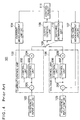
- FIG. 4 is an explanatory diagram illustrating a configuration of a conventional PI control device. This figure illustrates an example configuration of a PI control device 101 that performs feedback control (PI control) on a control object 111 such as, for example, a capacitor.
- PI control feedback control
- the PI control device 101 includes the following elements as a current control system: a reference input unit (A) 102 that receives an input of a set current value from outside, a current control unit 103 that performs PI control using this set current value, and a current measurement unit (A') 104 that measures the current flowing through the control object 111.
- a reference input unit (A) 102 that receives an input of a set current value from outside
- a current control unit 103 that performs PI control using this set current value
- A' current measurement unit
- the PI control device 101 further includes the following elements as a voltage control system: a reference input unit (B) 105 that receives an input of a set voltage value from outside, a voltage control unit 106 that performs PI control using this set voltage value, and a voltage measurement unit (B') 107 that measures the voltage generated in or being applied to the control object 111.
- a reference input unit (B) 105 that receives an input of a set voltage value from outside
- a voltage control unit 106 that performs PI control using this set voltage value
- a voltage measurement unit (B') 107 that measures the voltage generated in or being applied to the control object 111.
- An output point of the current control unit 103 and an output point of the voltage control unit 106 are connected to an output control unit 108 via a changeover switch 109.
- the changeover switch 109 is connected to a switching determination unit 110 that determines switching between the aforementioned current control and voltage control in accordance with, for example, the voltage output of the control object 111 or the like.
- the output control unit 108 includes, for example, a power semiconductor element, and is configured to output a voltage or current having a magnitude corresponding to a control signal (output voltage) or the like output from the current control unit 103 or the voltage control unit 106 to the control object 111.
- the current control unit 103 includes a subtractor 201 that determines a difference between the respective output values of the reference input unit (A) 102 and the current measurement unit (A') 104, a P control unit 202 that determines a P control value using the output value of the subtractor 201, an I control unit 203 that determines an I control value using the output value of the subtractor 201, and an adder 204 that adds together the respective output values of the P control unit 202 and the I control unit 203 to determine a PI control value.
- the voltage control unit 106 includes a subtractor 205 that determines a difference between the respective output values of the reference input unit (B) 105 and the voltage measurement unit (B') 107, a P control unit 206 that determines a P control value using the output value of the subtractor 205, an I control unit 207 that determines an I control value using the output value of the subtractor 205, and an adder 208 that adds together the respective output values of the P control unit 206 and the I control unit 207 to determine a PI control value.
- FIG 5 is an explanatory diagram illustrating a configuration of a conventional PID control device.
- An illustrated PID control device 120 has a similar configuration to the PI control device 101 in Figure 4 , except for a current control unit 121 and a voltage control unit 122.
- the current control unit 121 includes a subtractor 201, a P control unit 202, an I control unit 203, and an adder 204, and further includes a D control unit 210 that determines a D control value using the output value of the subtractor 201.
- the adder 204 of the current control unit 121 is configured to add together the respective output values of the P control unit 202, the I control unit 203, and the D control unit 210 and to output a PID control value.
- the voltage control unit 122 includes a subtractor 205, a P control unit 206, an I control unit 207, and an adder 208, and further includes a D control unit 211 that determines a D control value using the output value of the subtractor 205.
- the adder 208 of the voltage control unit 122 is configured to add together the respective output values of the P control unit 206, the I control unit 207, and the D control unit 211 and to determine a PID control value.
- the PID control device 120 in Figure 5 operates in a manner similar to the PI control device 101, except that it controls the control object 111 using values including the respective output values of the D control units 210 and 211, and the operation of the PI control device 101 will thus be representatively described here.
- the charging operation on the control object 111 will be exemplarily described. In the following, control switching is performed in a similar manner even if charging is substituted with discharging.
- the current control unit 103 determines, using the subtractor 201 included therein, the deviation of the measured value of the current flowing through the control object 111, which current is output from the current measurement unit (A') 104, from the aforementioned set current value, and the resulting value is input to the P control unit 202 and the I control unit 203.
- the respective values determined by the P control unit 202 and the I control unit 203 are added together using the adder 204 to determine a PI control value (current control value).
- the voltage control unit 106 determines, using the subtractor 205 included therein, the deviation of the measured value of the voltage across, for example, electrodes of the control object 111, which is output from the voltage measurement unit (B') 107, from the aforementioned set voltage value, and the resulting value is input to the P control unit 206 and the I control unit 207.
- the respective values determined by the P control unit 206 and the I control unit 207 are added together using the adder 208 to determine a PI (Integral) control value (voltage control value).
- Figure 6 includes explanatory diagrams illustrating the operation of the PI control device in Figure 4 . These figures illustrate a control operation when the switching determination unit 110 controls the changeover switch 109.
- Figure 6(a) illustrates the change in charging current supplied from the PI control device 101 to the control object 111 over time, with the vertical axis representing current values and the horizontal axis representing elapsed time.
- Figure 6(b) illustrates the change in, for example, the inter-electrode voltage of the control object 111 connected to the PI control device 101 over time, with the vertical axis representing voltage values and the horizontal axis representing elapsed time.
- Figure 6(c) illustrates the change in current control over time when a charging current is supplied to the control object 111 as described above, with the vertical axis representing current control values and the horizontal axis representing elapsed time. Note that, in Figure 6(c) , the P control value (graph (1)) output from the P control unit 202 and the I control value (graph (2)) output from the I control unit 203 are illustrated in terms of current control values.
- Figure 6(d) illustrates the change in voltage control over time when the charging current described above is supplied (a charging voltage is applied), with the vertical axis representing voltage control values and the horizontal axis representing elapsed time. Note that, in Figure 6(d) , the P control value (graph (3)) output from the P control unit 206 and the I control value (graph (4)) output from the I control unit 207 are illustrated in terms of voltage control value.
- the switching determination unit 110 controls the changeover switch 109 to connect the current control unit 103 and the output control unit 108 when charging begins.
- the current control unit 103 connected to the output control unit 108 performs PI control so that a charging current to be supplied to the control object 111 becomes equal to the set current value input from the reference input unit (A) 102.
- the current control unit 103 determines the deviation of the measured current value measured by the current measurement unit (A') 104 from the set current value described above, and adjusts the current control value, which is determined by P control and I control as illustrated in Figure 6(c) , to perform constant current control (PI control) so that the subsequent measured current values are set equal to the set current value and maintained constant.
- the switching determination unit 110 determines that a switching condition occurs at an illustrated point PI, and switches the connection of the changeover switch 109 to connect the voltage control unit 106 and the output control unit 108.
- the switching determination unit 110 switches from constant current control, which has just been performed, to constant voltage control at a point P2 in Figure 6(c) .
- the voltage control unit 106 When the voltage control unit 106 is connected to the output control unit 108 by the control switching described above, it determines a voltage control value for keeping the inter-electrode voltage of the control object 111 constant in a manner as depicted in a constant voltage control period illustrated in Figure 6(b) .
- the voltage control value output from the voltage control unit 106 is unstable in a manner depicted at a point P3 (varying period) illustrated in Figure 6(d) and particularly the voltage control value determined by I control markedly varies, making the voltage or the like being supplied to the control object 111 unstable.
- JP 2001 218487 A describes a controller for a servo motor with a current control means and a velocity control means, both of which perform calculations for PI control.
- Her-Terng Yau et al: "PSO Based PI Controller Design for a Solar Charger System", THE SCIENTIFIC WORLD JOURNAL, vol. 2013 describes a two-stage solar charging system that uses an intelligent algorithm to determine optimum PI charge control parameters.
- Patent reference 1 Japanese Patent No. 5122199
- a conventional feedback control device is configured in the manner described above, and thus has a problem in that when control switching is performed on binary parameters, a feedback control value varies, causing unstable control for a control object.
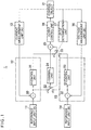
- Embodiment Figure 1 is an explanatory diagram illustrating a configuration of a feedback control device according to an embodiment of the present invention. This figure illustrates a PI control device 1, which is an example configuration of the feedback control device.
- the PI control device 1 includes a reference input unit (A) 11 that receives an input of a set current value from outside, a current control unit 12 that receives an input of the set current value through the reference input unit (A) 11 and that determines a control value for maintaining, for example, a charging current to be supplied to a control object 21 constant, and a current measurement unit (A') 13 that measures the current flowing through the control object 21 and that converts, for example, the measured current value into a signal in a predetermined form processible by a subtractor 30 or generates this signal.
- A reference input unit
- A current control unit 12 that receives an input of the set current value through the reference input unit (A) 11 and that determines a control value for maintaining, for example, a charging current to be supplied to a control object 21 constant
- a current measurement unit (A') 13 that measures the current flowing through the control object 21 and that converts, for example, the measured current value into a signal in a predetermined form processible by a subtractor 30 or
- the PI control device 1 further includes a reference input unit (B) 14 that receives an input of a set voltage value from outside, a voltage control unit 15 that receives an input of the set voltage value through the reference input unit (B) 14 and that determines a control value for maintaining, for example, a charging voltage to be applied to the control object 21 constant, and a voltage measurement unit (B') 16 that measures, for example, the inter-electrode voltage of the control object 21 and that converts, for example, this measured voltage value into a signal in a prescribed form processible by a subtractor 32 or generates this signal.
- a reference input unit (B) 14 that receives an input of a set voltage value from outside
- a voltage control unit 15 that receives an input of the set voltage value through the reference input unit (B) 14 and that determines a control value for maintaining, for example, a charging voltage to be applied to the control object 21 constant
- a voltage measurement unit (B') 16 that measures, for example, the inter-electrode voltage of
- the PI control device 1 includes an input changeover switch 22, an output changeover switch 23, an I control unit 24, an adder 25, an output control unit 26, and a u1/u2 determination unit 27.
- the control object 21 is an object on which prescribed control is to be performed by the output control unit 26 of the PI control device 1, and is, for example, a capacitor, a secondary cell or battery, or the like.
- the current control unit 12 includes the subtractor 30, which determines the deviation of the measured current value input from the current measurement unit (A') 13 from the set current value input from the reference input unit (A) 11, and a P control unit 31 that determines a P control value using the output value of the subtractor 30.
- the voltage control unit 15 includes the subtractor 32, which determines the deviation of the measured voltage value input from the voltage measurement unit (B') 16 from the set voltage value input from the reference input unit (B) 14, and a P control unit 33 that determines a P control value using the output value of the subtractor 32.
- An output point of the subtractor 30 is connected to an input point of the P control unit 31 and a contact u1 of the input changeover switch 22.
- An output point of the subtractor 32 is connected to an input point of the P control unit 33 and a contact u2 of the input changeover switch 22.
- a base b of the input changeover switch 22 is connected to an input point of the I control unit 24 that determines an I control value, and is configured to connect the output point of any one of the subtractor 30 and the subtractor 32 to the input point of the I control unit 24.
- An output point of the I control unit 24 is connected to a first input point of the adder 25. Further, a second input point of the adder 25 is connected to a base b of the output changeover switch 23.
- An output point of the P control unit 31 is connected to a contact u1 of the output changeover switch 23, and an output point of the P control unit 33 is connected to a contact u2 of the output changeover switch 23.
- a configuration is made such that the output point of any one of the P control unit 31 and the P control unit 33 is connected to the second input point of the adder 25.
- An output point of the adder 25 is connected to an input point of the output control unit 26, and is configured such that any one of a current control value generated by the current control unit 12 and the I control unit 24 (more specifically, a PI control value obtained by adding together the P control value output from the P control unit 31 and the I control value output from the I control unit 24) or a voltage control value generated by the voltage control unit 15 and the I control unit 24 (more specifically, a PI control value obtained by adding together the P control value output from the P control unit 33 and the I control value output from the I control unit 24) is input to the output control unit 26.
- a current control value generated by the current control unit 12 and the I control unit 24 more specifically, a PI control value obtained by adding together the P control value output from the P control unit 31 and the I control value output from the I control unit 24
- a voltage control value generated by the voltage control unit 15 and the I control unit 24 more specifically, a PI control value obtained by adding together the P control value output from the P control unit 33 and the I control
- the output control unit 26 is configured to control the control object 21 in accordance with a PI control value generated by the addition processing of the adder 25. Specifically, it is configured to supply, for example, a charging current corresponding to the aforementioned current control value to the control object 21, and is also configured to apply a charging voltage corresponding to the aforementioned voltage control value to the control object 21.
- the u1/u2 determination unit 27 is configured to monitor the state of the control object 21, and, more specifically, it includes a voltage detecting means for detecting, for example, the inter-electrode voltage of the control object 21, a current detecting means for detecting the value of the current flowing through the control object 21 (for example, the charging current being supplied to the control object 21, etc.), and so forth, and is configured to control the respective switching operations of the input changeover switch 22 and the output changeover switch 23 in accordance with the values detected by these detecting means.
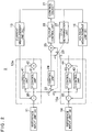
- Fig. 2 is an explanatory diagram illustrating another configuration of the feedback control device according to the embodiment of the present invention.
- This figure illustrates a PID control device 2, which is another example configuration of the feedback control device.
- the same numerals are used for portions identical to or corresponding to those illustrated in Fig. 1 , and a description thereof is omitted.
- a current control unit 12a included in the PID control device 2 includes a subtractor 30 and a P control unit 31, and further includes a D control unit 41 that determines a D (Differential) control value, and an adder 42. Further, a voltage control unit 15a includes a subtractor 32 and a P control unit unit 33, and further includes a D control unit 43 and an adder 44.
- the D control unit 41 of the current control unit 12a has an input point connected, together with an input point of the P control unit 31, to an output point of the subtractor 30 and a contact u1 of the input changeover switch 22.
- An output point of the D control unit 41 is connected to a first input point of the adder 42, and an output point of the P control unit 31 is connected to a second input point of the adder 42. That is, the D control unit 41 is connected in parallel with the P control unit 31, and is connected so as to receive an input of the same input value as that of the P control unit 31, that is, the output value of the subtractor 30. Furthermore, a connection is made such that the D control value determined by the D control unit 41 is input to the adder 42 and is added to the P control value determined by the P control unit 31.
- An output point of the adder 42 is connected to a contact u1 of the output changeover switch 23.
- the D control unit 43 of the voltage control unit 15a has an input point connected, together with an input point of the P control unit 33, to an output point of the subtractor 32 and a contact u2 of the input changeover switch 22.
- An output point of the D control unit 43 is connected to a first input point of the adder 44, and an output point of the P control unit 33 is connected to a second input point of the adder 44. That is, the D control unit 43 is connected in parallel with the P control unit 33, and is connected so as to receive an input of the same input value as that of the P control unit 33, that is, the output value of the subtractor 32. Furthermore, a connection is made such that the D control value determined by the D control unit 43 is input to the adder 44 and is added to the P control value determined by the P control unit 33.
- An output point of the adder 44 is connected to a contact u2 of the output changeover switch 23.
- the PID control device 2 illustrated in Figure 2 is configured in a manner similar to the PI control device 1 in Figure 1 , except that it includes the D control units 41 and 43 and the adders 42 and 44, and also operates in a similar manner in terms of the switching operation between constant current control and constant voltage control.
- the charging operation of the PI control device 1 illustrated in Figure 1 will be representatively described here. Note that the discharging operation in which two control loops are switched can also be performed in a similar way, in which case “charging” will be substituted with “discharging,” “increase” will be substituted with “decrease,” and so forth in the following description.
- Figure 3 includes explanatory diagrams illustrating the operation of the feedback control device according to the embodiment of the present invention. These figures illustrate a control operation when the u1/u2 determination unit 27 controls the changeover switches 22 and 23.
- the control object 21 is, for example, a lithium-ion secondary cell or battery
- charging is performed while a current value (a set current value set by the reference input unit (A) 11) specified in the specifications or the like of this lithium-ion secondary cell or battery is maintained when charging begins.
- a current value (a set current value set by the reference input unit (A) 11) specified in the specifications or the like of this lithium-ion secondary cell or battery is maintained when charging begins.
- a specified voltage a set voltage value set by the reference input unit (B) 14
- a period during which the constant-current charging described above is performed is represented as a “constant current control period,” and a period during which constant-voltage charging is performed with a set voltage value (the specified voltage described above) maintained is represented as a “constant voltage control period.”
- the set current value input from the reference input unit (A) 11 and the set voltage value input from the reference input unit (B) 14 are input from outside, as necessary, and are input to and set in the PI control device 1, for example, before the charging operation begins.
- Figure 3(a) illustrates the change in current supplied from the PI control device 1 to the control object 21 over time, with the vertical axis representing current values and the horizontal axis representing elapsed time.
- Figure 3(b) illustrates the change in, for example, the inter-electrode voltage of the control object 21 connected to the PI control device 1 over time, with the vertical axis representing voltage values and the horizontal axis representing elapsed time.
- Figure 3(c) illustrates the change in current control over time when a charging current is supplied to the control object 21 as described above, with the vertical axis representing current control values and the horizontal axis representing elapsed time. Note that, in Figure 3(c) , the P control value (graph (5)) output from the P control unit 31 and the I control value (graph (6)) output from the I control unit 24 are illustrated in terms of current control values.
- Figure 3(d) illustrates the transition in voltage control when the charging current described above is supplied (a charging voltage is applied), with the vertical axis representing voltage control values and the horizontal axis representing elapsed time. Note that, in Figure 3(d) , the P control value output from the P control unit 33 is illustrated in terms of voltage control. The I control value output from the I control unit 24 in this voltage control is as indicated by the graph (6) illustrated in the constant voltage control period in Figure 3(c) .
- the u1/u2 determination unit 27 connects the respective bases b of the input changeover switch 22 and the output changeover switch 23 to the contacts u1 in order to first perform charging by constant current control. That is, the output point of the subtractor 30 of the current control unit 12 and the input point of the I control unit 24 are connected to each other, and, in addition, the output point of the current control unit 12 (the P control unit 31) and the output point of the I control unit 24 are connected to the output control unit 26 through the adder 25.
- the set current value input from the reference input unit (A) 11 is input to the subtracter 30 together with the measured current value output from the current measurement unit (A') 13.
- the value (deviation) determined by the subtractor 30 is input to the P control unit 31 and is also input to the I control unit 24 via the input changeover switch 22 to determine a P control value and an I control value at this point in time.
- the I control value from the I control unit 24 is input to the adder 25, and the P control value from the P control unit 31 is input to the adder 25 via the output changeover switch 23.
- the adder 25 determines a PI control value from these control values, and outputs it to the output control unit 26.
- the output control unit 26 supplies a charging current corresponding to the input PI control value to the control object 21.
- This charging current the magnitude of which is measured by the current measurement unit (A') 13, is output as a measured current value at the next point in time to the subtractor 30.
- the subtractor 30 determines the deviation of the measured current value at the point in time described above from the aforementioned set current value (an input reference value), and outputs the resulting value to the P control unit 31 and also to the I control unit 24 via the input changeover switch 22.
- the P control unit 31 and the I control unit 24 determine a P control value and an I control value with respect to the new input value, and the adder 25 generates a new PI control value.
- This PI control value is input to the output control unit 26, and feedback control is performed to apply compensation so that, as illustrated in Figure 3(a) , a charging current to be supplied from the output control unit 26 to the control object 21 becomes equal to the set current value (in the illustrated constant current control period).
- a constant current control loop is formed by the P control unit 31, the I control unit 24, the adder 25, the output control unit 26, (the control object 21), the current measurement unit (A') 13, the subtractor 30, and so forth.
- the ul/u2 determination unit 27 When the ul/u2 determination unit 27 recognizes that the inter-electrode voltage of the control object 21 reaches the set voltage value at the time of a point P4 illustrated in Figure 3(b) , it switches the control of the charging operation from the constant current control to the constant voltage control. Specifically, the input changeover switch 22 and the output changeover switch 23 are controlled to connect the respective bases b of the switches from the contacts u1 to the contacts u2 in a switching manner.
- the I control unit 24 has received an input of the latest deviation for constant current control at the time of the point P4 at which the constant voltage control is started. That is, since the switching from the constant current control to the constant voltage control is performed in the state described above, the I control unit 24 always operates in a constant current control loop or a constant voltage control loop, and, as illustrated in graph (6) in Figure 3(c) , continues the output of I control values without greatly varying the I control value at the time of control switching.
- the contact connection of the output changeover switch 23 is switched so that the connection between the adder 25 and the P control unit 31 is disconnected and the P control unit 33 is connected to the input point of the adder 25. That is, the input of the P control value for constant current control from the P control unit 31 to the adder 25 is interrupted at a point P5 illustrated in Figure 3(c) , and the input of the P control value for constant voltage control from the P control unit 33 to the adder 25 is started at a point P6 illustrated in Figure 3(d) .
- the points P4 to P6 described above have time lengths that can be regarded as the same point in time within a charging period.
- the feedback control system used for constant voltage control that is, the voltage control unit 15 and so forth, is not included in a control loop that operates in the constant current control period in Figure 3 .
- the constant current control period As the charging operation progresses, the inter-electrode voltage of the control object 21 approaches the set voltage value. Accordingly, feedback control does not work in the constant current control period; however, the deviation determined by the subtractor 32 of the voltage control unit 15 decreases in this constant current control period as charging progresses, and the P control value determined by the P control unit 33 also transitions to a value in accordance with which a small amount of compensation is required.
- the P control unit 33 can generate a P control value for compensating for the charging voltage to be output from the output control unit 26 so that the charging voltage is equal to the set voltage value when the constant voltage control begins at the time of the point P6.
- an appropriate P control value is output from the P control unit 33 of the voltage control unit 15, and, in addition, as described previously, a substantially reasonable value is also output as a constant voltage control value from the I control unit 24. Accordingly, the PI control value to be input to the output control unit 26 does not greatly shift from an appropriate value at the time of switching from the constant current control to the constant voltage control. Thus, stable PI control can be continuously performed.
- the constant voltage control loop described above is formed by the P control unit 33, the I control unit 24, the adder 25, the output control unit 26, (the control object 21), the voltage measurement unit (B') 16, the subtractor 32, and so forth.
- the voltage measurement unit (B') 16 measures, for example, the inter-electrode voltage of the control object 21, and the subtractor 32 determines the deviation of the measured voltage value described above from the set voltage value. This deviation is input to the P control unit 33 and the I control unit 24 to determine a P control value and an I control value corresponding to this deviation.
- the adder 25 receives an input of the P control value and I control value described above, and determines a PI control value for constant voltage control.
- the output control unit 26 performs a control operation to apply compensation so that the voltage across the electrodes or the charging terminal of the control object 21 becomes equal to the set voltage value in accordance with the input PI control value for constant voltage control, and supplies a charging voltage to the control object 21.
- the charging operation under the constant voltage control described above is continuously performed until, for example, the charging current value measured by the current measurement unit (A') 13 is smaller than a preset value.
- control for the control object 21 is smoothly switched, and, as appropriate, a series of control operations is terminated.
- the current control unit 12 and the I control unit 24 are connected for constant current control, and the voltage control unit 15 and the I control unit 24 are connected for constant voltage control to generate a PI control value, and a charging current is supplied from the output control unit 26 to the control object 21. Accordingly, it is possible to prevent large variations in PI control value at the time of switching from the constant current control to the constant voltage control, and it is possible to perform stable control on the control object 21.
Landscapes
- Physics & Mathematics (AREA)
- General Physics & Mathematics (AREA)
- Engineering & Computer Science (AREA)
- Automation & Control Theory (AREA)
- Charge And Discharge Circuits For Batteries Or The Like (AREA)
- Feedback Control In General (AREA)
- Secondary Cells (AREA)
Description
- The present invention relates to a feedback control device that controls a control object by switching feedback control of binary parameters.
- For example, a step-up/step-down converter or the like that steps up and down an input voltage includes two-channel control means, and performs the respective feedback controls in a switching manner (see, for example, Patent reference 1). This device is configured to step up or down a power supply voltage to be supplied to a capacitor, a secondary cell or battery and then to perform a power running operation or a regeneration operation. Specifically, it includes a PI control system used to perform a step-up operation and a PI control system used to perform a step-down operation, and these control systems are connected to a power output means or the like in a switching manner to perform the respective device operations described above. In addition, some of the devices that perform two-channel feedback control perform continuous control while switching between, for example, constant current control and constant voltage control.
-
Figure 4 is an explanatory diagram illustrating a configuration of a conventional PI control device. This figure illustrates an example configuration of aPI control device 101 that performs feedback control (PI control) on acontrol object 111 such as, for example, a capacitor. - The
PI control device 101 includes the following elements as a current control system: a reference input unit (A) 102 that receives an input of a set current value from outside, acurrent control unit 103 that performs PI control using this set current value, and a current measurement unit (A') 104 that measures the current flowing through thecontrol object 111. - The
PI control device 101 further includes the following elements as a voltage control system: a reference input unit (B) 105 that receives an input of a set voltage value from outside, avoltage control unit 106 that performs PI control using this set voltage value, and a voltage measurement unit (B') 107 that measures the voltage generated in or being applied to thecontrol object 111. - An output point of the
current control unit 103 and an output point of thevoltage control unit 106 are connected to anoutput control unit 108 via achangeover switch 109. Thechangeover switch 109 is connected to aswitching determination unit 110 that determines switching between the aforementioned current control and voltage control in accordance with, for example, the voltage output of thecontrol object 111 or the like. - The
output control unit 108 includes, for example, a power semiconductor element, and is configured to output a voltage or current having a magnitude corresponding to a control signal (output voltage) or the like output from thecurrent control unit 103 or thevoltage control unit 106 to thecontrol object 111. - The
current control unit 103 includes asubtractor 201 that determines a difference between the respective output values of the reference input unit (A) 102 and the current measurement unit (A') 104, aP control unit 202 that determines a P control value using the output value of thesubtractor 201, anI control unit 203 that determines an I control value using the output value of thesubtractor 201, and anadder 204 that adds together the respective output values of theP control unit 202 and theI control unit 203 to determine a PI control value. - The
voltage control unit 106 includes asubtractor 205 that determines a difference between the respective output values of the reference input unit (B) 105 and the voltage measurement unit (B') 107, aP control unit 206 that determines a P control value using the output value of thesubtractor 205, anI control unit 207 that determines an I control value using the output value of thesubtractor 205, and anadder 208 that adds together the respective output values of theP control unit 206 and theI control unit 207 to determine a PI control value. -
Figure 5 is an explanatory diagram illustrating a configuration of a conventional PID control device. An illustratedPID control device 120 has a similar configuration to thePI control device 101 inFigure 4 , except for acurrent control unit 121 and avoltage control unit 122. - The
current control unit 121 includes asubtractor 201, aP control unit 202, anI control unit 203, and anadder 204, and further includes aD control unit 210 that determines a D control value using the output value of thesubtractor 201. Theadder 204 of thecurrent control unit 121 is configured to add together the respective output values of theP control unit 202, theI control unit 203, and theD control unit 210 and to output a PID control value. - The
voltage control unit 122 includes asubtractor 205, aP control unit 206, anI control unit 207, and anadder 208, and further includes aD control unit 211 that determines a D control value using the output value of thesubtractor 205. Theadder 208 of thevoltage control unit 122 is configured to add together the respective output values of theP control unit 206, theI control unit 207, and theD control unit 211 and to determine a PID control value. - Next, the operation will be described.
- The
PID control device 120 inFigure 5 operates in a manner similar to thePI control device 101, except that it controls thecontrol object 111 using values including the respective output values of theD control units PI control device 101 will thus be representatively described here. In addition, the charging operation on thecontrol object 111 will be exemplarily described. In the following, control switching is performed in a similar manner even if charging is substituted with discharging. - When a set current value is input to the
current control unit 103 from outside through the reference input unit (A) 102 in the manner described previously, thecurrent control unit 103 determines, using thesubtractor 201 included therein, the deviation of the measured value of the current flowing through thecontrol object 111, which current is output from the current measurement unit (A') 104, from the aforementioned set current value, and the resulting value is input to theP control unit 202 and theI control unit 203. The respective values determined by theP control unit 202 and theI control unit 203 are added together using theadder 204 to determine a PI control value (current control value). - Further, when a set voltage value is input to the
voltage control unit 106 from outside through the reference input unit (B) 105, thevoltage control unit 106 determines, using thesubtractor 205 included therein, the deviation of the measured value of the voltage across, for example, electrodes of thecontrol object 111, which is output from the voltage measurement unit (B') 107, from the aforementioned set voltage value, and the resulting value is input to theP control unit 206 and theI control unit 207. The respective values determined by theP control unit 206 and theI control unit 207 are added together using theadder 208 to determine a PI (Integral) control value (voltage control value). -
Figure 6 includes explanatory diagrams illustrating the operation of the PI control device inFigure 4 . These figures illustrate a control operation when theswitching determination unit 110 controls thechangeover switch 109. -
Figure 6(a) illustrates the change in charging current supplied from thePI control device 101 to thecontrol object 111 over time, with the vertical axis representing current values and the horizontal axis representing elapsed time. -
Figure 6(b) illustrates the change in, for example, the inter-electrode voltage of thecontrol object 111 connected to thePI control device 101 over time, with the vertical axis representing voltage values and the horizontal axis representing elapsed time. -
Figure 6(c) illustrates the change in current control over time when a charging current is supplied to thecontrol object 111 as described above, with the vertical axis representing current control values and the horizontal axis representing elapsed time. Note that, inFigure 6(c) , the P control value (graph (1)) output from theP control unit 202 and the I control value (graph (2)) output from theI control unit 203 are illustrated in terms of current control values. -
Figure 6(d) illustrates the change in voltage control over time when the charging current described above is supplied (a charging voltage is applied), with the vertical axis representing voltage control values and the horizontal axis representing elapsed time. Note that, inFigure 6(d) , the P control value (graph (3)) output from theP control unit 206 and the I control value (graph (4)) output from theI control unit 207 are illustrated in terms of voltage control value. - In a case where the
control object 111 is, for example, a lithium-ion secondary cell or battery and a charging current is to be supplied to thecontrol object 111, theswitching determination unit 110 controls thechangeover switch 109 to connect thecurrent control unit 103 and theoutput control unit 108 when charging begins. Thecurrent control unit 103 connected to theoutput control unit 108 performs PI control so that a charging current to be supplied to thecontrol object 111 becomes equal to the set current value input from the reference input unit (A) 102. - In this case, the
current control unit 103 determines the deviation of the measured current value measured by the current measurement unit (A') 104 from the set current value described above, and adjusts the current control value, which is determined by P control and I control as illustrated inFigure 6(c) , to perform constant current control (PI control) so that the subsequent measured current values are set equal to the set current value and maintained constant. - As described previously, when, with the progress of charging by constant current control, as illustrated in
Figure 6(b) , the voltage value of thecontrol object 111 increases and reaches the set voltage value input by the reference input unit (B) 105, theswitching determination unit 110 determines that a switching condition occurs at an illustrated point PI, and switches the connection of thechangeover switch 109 to connect thevoltage control unit 106 and theoutput control unit 108. - In other words, for example, when the measured voltage value of the voltage measurement unit (B') 107 reaches the set voltage value, the
switching determination unit 110 switches from constant current control, which has just been performed, to constant voltage control at a point P2 inFigure 6(c) . - When the
voltage control unit 106 is connected to theoutput control unit 108 by the control switching described above, it determines a voltage control value for keeping the inter-electrode voltage of thecontrol object 111 constant in a manner as depicted in a constant voltage control period illustrated inFigure 6(b) . - Immediately after the
switching determination unit 110 has performed switching from constant current control to constant voltage control, the voltage control value output from thevoltage control unit 106 is unstable in a manner depicted at a point P3 (varying period) illustrated inFigure 6(d) and particularly the voltage control value determined by I control markedly varies, making the voltage or the like being supplied to thecontrol object 111 unstable.
JP 2001 218487 A - Patent reference 1: Japanese Patent No.
5122199 - A conventional feedback control device is configured in the manner described above, and thus has a problem in that when control switching is performed on binary parameters, a feedback control value varies, causing unstable control for a control object.
- According to an aspect of the present invention there is provided a feedback control device as claimed in
claim 1. - According to the present invention, it is possible to reduce variations in control value when switching is performed from first feedback control to second feedback control, and it is possible to achieve smooth continuous feedback control.
-
-
Figure 1 is an explanatory diagram illustrating a configuration of a feedback control device according to an embodiment of the present invention. -
Figure 2 is an explanatory diagram illustrating another configuration of the feedback control device according to the embodiment of the present invention. -
Figure 3 includes explanatory diagrams illustrating the operation of the feedback control device according to the embodiment of the present invention. -
Figure 4 is an explanatory diagram illustrating a configuration of a conventional PI control device. -
Figure 5 is an explanatory diagram illustrating a configuration of a conventional PID control device. -
Figure 6 is an explanatory diagram illustrating the operation of the PI control device inFigure 4 . - An embodiment of the present invention will be described hereinafter. Embodiment
Figure 1 is an explanatory diagram illustrating a configuration of a feedback control device according to an embodiment of the present invention. This figure illustrates aPI control device 1, which is an example configuration of the feedback control device. - The
PI control device 1 includes a reference input unit (A) 11 that receives an input of a set current value from outside, acurrent control unit 12 that receives an input of the set current value through the reference input unit (A) 11 and that determines a control value for maintaining, for example, a charging current to be supplied to acontrol object 21 constant, and a current measurement unit (A') 13 that measures the current flowing through thecontrol object 21 and that converts, for example, the measured current value into a signal in a predetermined form processible by asubtractor 30 or generates this signal. - The
PI control device 1 further includes a reference input unit (B) 14 that receives an input of a set voltage value from outside, avoltage control unit 15 that receives an input of the set voltage value through the reference input unit (B) 14 and that determines a control value for maintaining, for example, a charging voltage to be applied to thecontrol object 21 constant, and a voltage measurement unit (B') 16 that measures, for example, the inter-electrode voltage of thecontrol object 21 and that converts, for example, this measured voltage value into a signal in a prescribed form processible by asubtractor 32 or generates this signal. - Furthermore, the
PI control device 1 includes aninput changeover switch 22, anoutput changeover switch 23, anI control unit 24, anadder 25, anoutput control unit 26, and a u1/u2 determination unit 27. - The
control object 21 is an object on which prescribed control is to be performed by theoutput control unit 26 of thePI control device 1, and is, for example, a capacitor, a secondary cell or battery, or the like. - Here, supply of charging power to the
control object 21 will be exemplarily described. - The
current control unit 12 includes thesubtractor 30, which determines the deviation of the measured current value input from the current measurement unit (A') 13 from the set current value input from the reference input unit (A) 11, and aP control unit 31 that determines a P control value using the output value of thesubtractor 30. - The
voltage control unit 15 includes thesubtractor 32, which determines the deviation of the measured voltage value input from the voltage measurement unit (B') 16 from the set voltage value input from the reference input unit (B) 14, and aP control unit 33 that determines a P control value using the output value of thesubtractor 32. - An output point of the
subtractor 30 is connected to an input point of theP control unit 31 and a contact u1 of theinput changeover switch 22. - An output point of the
subtractor 32 is connected to an input point of theP control unit 33 and a contact u2 of theinput changeover switch 22. - A base b of the
input changeover switch 22 is connected to an input point of theI control unit 24 that determines an I control value, and is configured to connect the output point of any one of thesubtractor 30 and thesubtractor 32 to the input point of theI control unit 24. - An output point of the
I control unit 24 is connected to a first input point of theadder 25. Further, a second input point of theadder 25 is connected to a base b of theoutput changeover switch 23. - An output point of the
P control unit 31 is connected to a contact u1 of theoutput changeover switch 23, and an output point of theP control unit 33 is connected to a contact u2 of theoutput changeover switch 23. A configuration is made such that the output point of any one of theP control unit 31 and theP control unit 33 is connected to the second input point of theadder 25. - An output point of the
adder 25 is connected to an input point of theoutput control unit 26, and is configured such that any one of a current control value generated by thecurrent control unit 12 and the I control unit 24 (more specifically, a PI control value obtained by adding together the P control value output from theP control unit 31 and the I control value output from the I control unit 24) or a voltage control value generated by thevoltage control unit 15 and the I control unit 24 (more specifically, a PI control value obtained by adding together the P control value output from theP control unit 33 and the I control value output from the I control unit 24) is input to theoutput control unit 26. - The
output control unit 26 is configured to control thecontrol object 21 in accordance with a PI control value generated by the addition processing of theadder 25. Specifically, it is configured to supply, for example, a charging current corresponding to the aforementioned current control value to thecontrol object 21, and is also configured to apply a charging voltage corresponding to the aforementioned voltage control value to thecontrol object 21. - The u1/
u2 determination unit 27 is configured to monitor the state of thecontrol object 21, and, more specifically, it includes a voltage detecting means for detecting, for example, the inter-electrode voltage of thecontrol object 21, a current detecting means for detecting the value of the current flowing through the control object 21 (for example, the charging current being supplied to thecontrol object 21, etc.), and so forth, and is configured to control the respective switching operations of theinput changeover switch 22 and theoutput changeover switch 23 in accordance with the values detected by these detecting means. -
Fig. 2 is an explanatory diagram illustrating another configuration of the feedback control device according to the embodiment of the present invention. This figure illustrates aPID control device 2, which is another example configuration of the feedback control device. The same numerals are used for portions identical to or corresponding to those illustrated inFig. 1 , and a description thereof is omitted. - A
current control unit 12a included in thePID control device 2 includes asubtractor 30 and aP control unit 31, and further includes aD control unit 41 that determines a D (Differential) control value, and anadder 42. Further, avoltage control unit 15a includes asubtractor 32 and a Pcontrol unit unit 33, and further includes aD control unit 43 and anadder 44. - The
D control unit 41 of thecurrent control unit 12a has an input point connected, together with an input point of theP control unit 31, to an output point of thesubtractor 30 and a contact u1 of theinput changeover switch 22. - An output point of the
D control unit 41 is connected to a first input point of theadder 42, and an output point of theP control unit 31 is connected to a second input point of theadder 42. That is, theD control unit 41 is connected in parallel with theP control unit 31, and is connected so as to receive an input of the same input value as that of theP control unit 31, that is, the output value of thesubtractor 30. Furthermore, a connection is made such that the D control value determined by theD control unit 41 is input to theadder 42 and is added to the P control value determined by theP control unit 31. - An output point of the
adder 42 is connected to a contact u1 of theoutput changeover switch 23. - The
D control unit 43 of thevoltage control unit 15a has an input point connected, together with an input point of theP control unit 33, to an output point of thesubtractor 32 and a contact u2 of theinput changeover switch 22. - An output point of the
D control unit 43 is connected to a first input point of theadder 44, and an output point of theP control unit 33 is connected to a second input point of theadder 44. That is, theD control unit 43 is connected in parallel with theP control unit 33, and is connected so as to receive an input of the same input value as that of theP control unit 33, that is, the output value of thesubtractor 32. Furthermore, a connection is made such that the D control value determined by theD control unit 43 is input to theadder 44 and is added to the P control value determined by theP control unit 33. - An output point of the
adder 44 is connected to a contact u2 of theoutput changeover switch 23. - Next, the operation will be described.
- The
PID control device 2 illustrated inFigure 2 is configured in a manner similar to thePI control device 1 inFigure 1 , except that it includes theD control units adders PI control device 1 illustrated inFigure 1 will be representatively described here. Note that the discharging operation in which two control loops are switched can also be performed in a similar way, in which case "charging" will be substituted with "discharging," "increase" will be substituted with "decrease," and so forth in the following description. -
Figure 3 includes explanatory diagrams illustrating the operation of the feedback control device according to the embodiment of the present invention. These figures illustrate a control operation when the u1/u2 determination unit 27 controls the changeover switches 22 and 23. - In a case where the
control object 21 is, for example, a lithium-ion secondary cell or battery, charging is performed while a current value (a set current value set by the reference input unit (A) 11) specified in the specifications or the like of this lithium-ion secondary cell or battery is maintained when charging begins. In addition, when the inter-electrode voltage of the lithium-ion secondary cell or battery increases due to this constant-current charging and this voltage value reaches a specified voltage (a set voltage value set by the reference input unit (B) 14) determined based on the specifications or the like of the lithium-ion secondary cell or battery, constant-voltage charging is continuously performed with this specified voltage maintained. - PI control in the charging operation of a lithium-ion secondary cell or battery will be exemplarily described here.
- In
Figure 3 , a period during which the constant-current charging described above is performed is represented as a "constant current control period," and a period during which constant-voltage charging is performed with a set voltage value (the specified voltage described above) maintained is represented as a "constant voltage control period." - Note that the set current value input from the reference input unit (A) 11 and the set voltage value input from the reference input unit (B) 14 are input from outside, as necessary, and are input to and set in the
PI control device 1, for example, before the charging operation begins. -
Figure 3(a) illustrates the change in current supplied from thePI control device 1 to thecontrol object 21 over time, with the vertical axis representing current values and the horizontal axis representing elapsed time. -
Figure 3(b) illustrates the change in, for example, the inter-electrode voltage of thecontrol object 21 connected to thePI control device 1 over time, with the vertical axis representing voltage values and the horizontal axis representing elapsed time. -
Figure 3(c) illustrates the change in current control over time when a charging current is supplied to thecontrol object 21 as described above, with the vertical axis representing current control values and the horizontal axis representing elapsed time. Note that, inFigure 3(c) , the P control value (graph (5)) output from theP control unit 31 and the I control value (graph (6)) output from theI control unit 24 are illustrated in terms of current control values. -
Figure 3(d) illustrates the transition in voltage control when the charging current described above is supplied (a charging voltage is applied), with the vertical axis representing voltage control values and the horizontal axis representing elapsed time. Note that, inFigure 3(d) , the P control value output from theP control unit 33 is illustrated in terms of voltage control. The I control value output from theI control unit 24 in this voltage control is as indicated by the graph (6) illustrated in the constant voltage control period inFigure 3(c) . - In a case where the
control object 21 is a lithium-ion secondary cell or battery or the like, when a charging current is to be supplied to thecontrol object 21, the u1/u2 determination unit 27 connects the respective bases b of theinput changeover switch 22 and theoutput changeover switch 23 to the contacts u1 in order to first perform charging by constant current control. That is, the output point of thesubtractor 30 of thecurrent control unit 12 and the input point of theI control unit 24 are connected to each other, and, in addition, the output point of the current control unit 12 (the P control unit 31) and the output point of theI control unit 24 are connected to theoutput control unit 26 through theadder 25. - In the switch connection state described above, the set current value input from the reference input unit (A) 11 is input to the
subtracter 30 together with the measured current value output from the current measurement unit (A') 13. - The value (deviation) determined by the
subtractor 30 is input to theP control unit 31 and is also input to theI control unit 24 via theinput changeover switch 22 to determine a P control value and an I control value at this point in time. - The I control value from the
I control unit 24 is input to theadder 25, and the P control value from theP control unit 31 is input to theadder 25 via theoutput changeover switch 23. Theadder 25 determines a PI control value from these control values, and outputs it to theoutput control unit 26. - The
output control unit 26 supplies a charging current corresponding to the input PI control value to thecontrol object 21. This charging current, the magnitude of which is measured by the current measurement unit (A') 13, is output as a measured current value at the next point in time to thesubtractor 30. - The
subtractor 30 determines the deviation of the measured current value at the point in time described above from the aforementioned set current value (an input reference value), and outputs the resulting value to theP control unit 31 and also to theI control unit 24 via theinput changeover switch 22. - Thereafter, the
P control unit 31 and theI control unit 24 determine a P control value and an I control value with respect to the new input value, and theadder 25 generates a new PI control value. This PI control value is input to theoutput control unit 26, and feedback control is performed to apply compensation so that, as illustrated inFigure 3(a) , a charging current to be supplied from theoutput control unit 26 to thecontrol object 21 becomes equal to the set current value (in the illustrated constant current control period). - In the constant current control, as described above, a constant current control loop is formed by the
P control unit 31, theI control unit 24, theadder 25, theoutput control unit 26, (the control object 21), the current measurement unit (A') 13, thesubtractor 30, and so forth. - As described previously, supplying a charging current that is maintained constant to the
control object 21 increases the voltage value across the electrodes or across a charging terminal of thecontrol object 21 in the manner illustrated inFigure 3(b) . - When the ul/
u2 determination unit 27 recognizes that the inter-electrode voltage of thecontrol object 21 reaches the set voltage value at the time of a point P4 illustrated inFigure 3(b) , it switches the control of the charging operation from the constant current control to the constant voltage control. Specifically, theinput changeover switch 22 and theoutput changeover switch 23 are controlled to connect the respective bases b of the switches from the contacts u1 to the contacts u2 in a switching manner. - The I control
unit 24 has received an input of the latest deviation for constant current control at the time of the point P4 at which the constant voltage control is started. That is, since the switching from the constant current control to the constant voltage control is performed in the state described above, theI control unit 24 always operates in a constant current control loop or a constant voltage control loop, and, as illustrated in graph (6) inFigure 3(c) , continues the output of I control values without greatly varying the I control value at the time of control switching. - In the control switching at the time of the point P4, furthermore, as described previously, the contact connection of the
output changeover switch 23 is switched so that the connection between theadder 25 and theP control unit 31 is disconnected and theP control unit 33 is connected to the input point of theadder 25. That is, the input of the P control value for constant current control from theP control unit 31 to theadder 25 is interrupted at a point P5 illustrated inFigure 3(c) , and the input of the P control value for constant voltage control from theP control unit 33 to theadder 25 is started at a point P6 illustrated inFigure 3(d) . Note that the points P4 to P6 described above have time lengths that can be regarded as the same point in time within a charging period. - The feedback control system used for constant voltage control, that is, the
voltage control unit 15 and so forth, is not included in a control loop that operates in the constant current control period inFigure 3 . In the constant current control period, as the charging operation progresses, the inter-electrode voltage of thecontrol object 21 approaches the set voltage value. Accordingly, feedback control does not work in the constant current control period; however, the deviation determined by thesubtractor 32 of thevoltage control unit 15 decreases in this constant current control period as charging progresses, and the P control value determined by theP control unit 33 also transitions to a value in accordance with which a small amount of compensation is required. - From the foregoing, the
P control unit 33 can generate a P control value for compensating for the charging voltage to be output from theoutput control unit 26 so that the charging voltage is equal to the set voltage value when the constant voltage control begins at the time of the point P6. - In this manner, an appropriate P control value is output from the
P control unit 33 of thevoltage control unit 15, and, in addition, as described previously, a substantially reasonable value is also output as a constant voltage control value from theI control unit 24. Accordingly, the PI control value to be input to theoutput control unit 26 does not greatly shift from an appropriate value at the time of switching from the constant current control to the constant voltage control. Thus, stable PI control can be continuously performed. - In order to maintain the set voltage value input from the reference input unit (B) 14 in advance constant as a charging voltage in the "constant voltage control period" illustrated in
Figure 3 , as described previously, the connections of the respective bases b of theinput changeover switch 22 and theoutput changeover switch 23 are switched from the contacts u1 to the contacts u2 by control of the u1/u2 determination unit 27, allowing thevoltage control unit 15 and so forth to operate to perform feedback control using a constant voltage control loop. - The constant voltage control loop described above is formed by the
P control unit 33, theI control unit 24, theadder 25, theoutput control unit 26, (the control object 21), the voltage measurement unit (B') 16, thesubtractor 32, and so forth. - Specifically, the voltage measurement unit (B') 16 measures, for example, the inter-electrode voltage of the
control object 21, and thesubtractor 32 determines the deviation of the measured voltage value described above from the set voltage value. This deviation is input to theP control unit 33 and theI control unit 24 to determine a P control value and an I control value corresponding to this deviation. - The
adder 25 receives an input of the P control value and I control value described above, and determines a PI control value for constant voltage control. Theoutput control unit 26 performs a control operation to apply compensation so that the voltage across the electrodes or the charging terminal of thecontrol object 21 becomes equal to the set voltage value in accordance with the input PI control value for constant voltage control, and supplies a charging voltage to thecontrol object 21. The charging operation under the constant voltage control described above is continuously performed until, for example, the charging current value measured by the current measurement unit (A') 13 is smaller than a preset value. - In this way, control for the
control object 21 is smoothly switched, and, as appropriate, a series of control operations is terminated. - As described above, according to this embodiment, the
current control unit 12 and theI control unit 24 are connected for constant current control, and thevoltage control unit 15 and theI control unit 24 are connected for constant voltage control to generate a PI control value, and a charging current is supplied from theoutput control unit 26 to thecontrol object 21. Accordingly, it is possible to prevent large variations in PI control value at the time of switching from the constant current control to the constant voltage control, and it is possible to perform stable control on thecontrol object 21. -
- 1
- PI control device
- 2
- PID control device
- 11
- reference input unit (A)
- 12, 12a
- current control unit
- 13
- current measurement unit (A')
- 14
- reference input unit (B)
- 15, 15a
- voltage control unit
- 16
- voltage measurement unit (B')
- 21
- control object
- 22
- input changeover switch
- 23
- output changeover switch
- 24
- I (Integral) control unit
- 25, 42, 44
- adder
- 26
- output control unit
- 27
- u1/u2 determination unit (switching determination unit)
- 30, 32
- subtractor
- 31, 33
- P (Proportional) control unit
- 41, 43
- D (Differential) control unit
- 101
- PI control device
- 102
- reference input unit (A)
- 103
- current control unit
- 104
- current measurement unit (A')
- 105
- reference input unit (B)
- 106
- voltage control unit
- 107
- voltage measurement unit (B')
- 108
- output control unit
- 109
- changeover switch
- 110
- u1/u2 determination unit (switching determination unit)
- 120
- PID control device
- 111
- control object
- 121
- current control unit
- 122
- voltage control unit
- 201,205
- subtractor
- 202, 206
- P (Proportional) control unit
- 203, 207
- I (Integral) control unit
- 204, 208
- adder
- 210, 211
- D (Differential) control unit
Claims (3)
- A feedback control device comprising:a current control unit (12, 12a) that includes a first proportional control unit (31) and that is arranged to perform constant current control on an object (21) charging or discharging power;a voltage control unit (15, 15a) that includes a second proportional control unit (33) and that is arranged to perform constant voltage control on the object (21);a single integral control unit(24) used for the constant current control and the constant voltage control;a first subtracter (30) arranged to obtain a deviation of a current value of the object (21) measured by a current measurement unit (13) from a preset current value, and input the deviation to the first proportional control unit (31),a second subtractor (32) arranged to obtain a deviation of a voltage value of the object (21) measured by a voltage measurement unit(16) from a preset voltage and input the deviation to the second proportional control unit (33)an adder (25) that has as an input an output control value of the integral control unit (24), and that is arranged to add the output control value of the integral control unit(24) to an output control value that is output from the current control unit (12, 12a) or from the voltage control unit (15, 15a),an output control unit (26) arranged to control charging or discharging of the object using a control value that is output from the adder (25);a first changeover switch (22) arranged to select one of the deviation that is output from the subtractor (30) and the deviation that is output from the subtractor (32), and arranged to input the thus selected deviation to the integral control unit (24);a second changeover switch (23) arranged to select one of the control value that is output from the current control unit(12, 12a) and the control value that is output from the voltage control unit (15, 15a), and arranged to input the thus selected control value to the adder (25), anda switching determination unit(27) arranged to determine a voltage of the object (21) to control an operation of the first changeover switch (22) and the second changeover switch (23), whereina constant current loop of the object (21) is formed by the current measurement unit (13), the first subtracter (30), the current control unit (12, 12a), the integral control unit (24), the adder (25), and the output control unit (26),a constant voltage loop of the object (21) is formed by the voltage measurement unit (16), the second subtractor (32), the voltage control unit (15, 15a), the integral control unit (24), the adder (25) and the output control unit (26),and in use the switching determination unit (27)
controls the first changeover switch (22) and second changeover switch (23) to form the constant current control loop, and adds an output control value of the current control unit(12, 12a) and an output value of the integral control unit (24) to perform constant current control, and
when the switch determination unit (27) recognizes that the voltage of the object (21) reaches the preset voltage value under the constant current control, the switching determination unit (27)controls the changeover switch (22) and the changeover switch (23) to form the constant voltage control loop, adds the output control value of the voltage control unit (15, 15a) and the output control value of the integral control unit(24) to perform the constant voltage control, andcontinues to output the output control value of the integral control unit (24) when changing from constant current control to constant voltage control. - The feedback control device according to claim 1, wherein in use
a first PI control is performed on the object (21) as the constant current control and second PI control is performed on the object (21) as the constant voltage control. - The feedback control device according to Claim 1 wherein the current control unit (12a) further includes a first differential control unit (41), that has as an input the output of the first subtractor (30), a second adder (42) that is arranged to add the output of the first differential control unit (41) to the output of the first proportional control unit (31), the voltage control unit (15a) further includes a second differential control unit (43), that has as an input the output of the second subtractor (32), a third adder (44) that is arranged to add the output of the second differential control unit (43) to the output of the second proportional control unit (33), and in use
a first PID control is performed on the object (21) as the constant current control and a second PID control is performed on the object (21) as the constant voltage control.
Applications Claiming Priority (1)
| Application Number | Priority Date | Filing Date | Title |
|---|---|---|---|
| PCT/IB2014/001502 WO2016020717A1 (en) | 2014-08-08 | 2014-08-08 | Feedback control device |
Publications (3)
| Publication Number | Publication Date |
|---|---|
| EP3177971A1 EP3177971A1 (en) | 2017-06-14 |
| EP3177971A4 EP3177971A4 (en) | 2018-07-11 |
| EP3177971B1 true EP3177971B1 (en) | 2020-02-12 |
Family
ID=55263215
Family Applications (1)
| Application Number | Title | Priority Date | Filing Date |
|---|---|---|---|
| EP14899488.2A Active EP3177971B1 (en) | 2014-08-08 | 2014-08-08 | Feedback control device |
Country Status (5)
| Country | Link |
|---|---|
| US (1) | US10234830B2 (en) |
| EP (1) | EP3177971B1 (en) |
| JP (1) | JP6376370B2 (en) |
| CN (1) | CN106716268B (en) |
| WO (1) | WO2016020717A1 (en) |
Families Citing this family (6)
| Publication number | Priority date | Publication date | Assignee | Title |
|---|---|---|---|---|
| IT201700100704A1 (en) * | 2017-09-08 | 2019-03-08 | Nuovo Pignone Tecnologie Srl | CONTROL SYSTEM FOR A COMPRESSOR WITH A PRESSURE-BASED SUBSYSTEM, SYNTHESIS SYSTEM AND CONTROL SYSTEM / CONTROL SYSTEM FOR A COMPRESSOR WITH PRESSURE-BASED SUBSYSTEM, SYNTHESIS PLANT AND CONTROL METHOD |
| IT201700100734A1 (en) * | 2017-09-08 | 2019-03-08 | Nuovo Pignone Tecnologie Srl | CONTROL SYSTEM FOR A COMPRESSOR WITH SPEED BASED SUBSYSTEM, SYNTHESIS SYSTEM AND CONTROL SYSTEM / CONTROL SYSTEM FOR A COMPRESSOR WITH SPEED-BASED SUBSYSTEM, SYNTHESIS PLANT AND CONTROL METHOD |
| JP6958808B2 (en) * | 2017-09-15 | 2021-11-02 | 富士通株式会社 | Policy improvement programs, policy improvement methods, and policy improvement devices |
| JP7378380B2 (en) * | 2020-11-04 | 2023-11-13 | 株式会社日立製作所 | Proportional-integral control device and proportional-integral control method |
| CN113922462B (en) * | 2021-10-28 | 2024-10-01 | 新风光电子科技股份有限公司 | A floating charge control method based on feedforward control for energy storage converter |
| CN116044565A (en) * | 2023-01-12 | 2023-05-02 | 兰州电机股份有限公司 | Coaxial double-output generator set and control method thereof |
Family Cites Families (8)
| Publication number | Priority date | Publication date | Assignee | Title |
|---|---|---|---|---|
| JP2781144B2 (en) * | 1994-12-08 | 1998-07-30 | 三菱電機株式会社 | Control method of AC / DC converter |
| JP2001218487A (en) * | 2000-01-31 | 2001-08-10 | Tokimec Inc | Controller for servo motor |
| JP5122199B2 (en) * | 2007-07-20 | 2013-01-16 | 住友重機械工業株式会社 | Control device for buck-boost converter |
| EP2763270B1 (en) * | 2011-09-27 | 2016-05-25 | Toyota Jidosha Kabushiki Kaisha | Power supply system and method for controlling same |
| CN103076739A (en) * | 2012-09-07 | 2013-05-01 | 北京航空航天大学 | Self-feedback drive control system of double shape memory alloy wires and testing platform of drive control system |
| CN103078545B (en) * | 2013-01-15 | 2015-02-25 | 东华大学 | Control circuit for stand-alone /grid-connected dual-mode inverter and switching technology thereof |
| CN103281036B (en) * | 2013-05-16 | 2015-09-30 | 浙江吉利汽车研究院有限公司杭州分公司 | Control method and control device of five-phase alternating current motor |
| US9442140B2 (en) * | 2014-03-12 | 2016-09-13 | Qualcomm Incorporated | Average current mode control of multi-phase switching power converters |
-
2014
- 2014-08-08 JP JP2017506978A patent/JP6376370B2/en active Active
- 2014-08-08 WO PCT/IB2014/001502 patent/WO2016020717A1/en not_active Ceased
- 2014-08-08 CN CN201480081775.4A patent/CN106716268B/en active Active
- 2014-08-08 US US15/501,886 patent/US10234830B2/en active Active
- 2014-08-08 EP EP14899488.2A patent/EP3177971B1/en active Active
Non-Patent Citations (1)
| Title |
|---|
| None * |
Also Published As
| Publication number | Publication date |
|---|---|
| WO2016020717A1 (en) | 2016-02-11 |
| CN106716268A (en) | 2017-05-24 |
| JP2017523532A (en) | 2017-08-17 |
| US10234830B2 (en) | 2019-03-19 |
| JP6376370B2 (en) | 2018-08-22 |
| CN106716268B (en) | 2020-01-10 |
| EP3177971A4 (en) | 2018-07-11 |
| EP3177971A1 (en) | 2017-06-14 |
| US20170227936A1 (en) | 2017-08-10 |
Similar Documents
| Publication | Publication Date | Title |
|---|---|---|
| JP5455705B2 (en) | Charging device and charging method | |
| US10234830B2 (en) | Feedback control device | |
| JP4660523B2 (en) | Charging system that controls charging at the surface temperature of the battery cell | |
| CN105337335B (en) | System and method for matching end of discharge for multiple batteries | |
| JP6145712B2 (en) | Secondary battery charging system and method, and battery pack | |
| WO2015181847A1 (en) | Battery charger | |
| CN101496256A (en) | Power supply unit for charging | |
| EP3143675B1 (en) | Battery charger for different power sources | |
| US20210126470A1 (en) | Closed Loop Headroom Management For Battery Charging | |
| CN104137377A (en) | Method for synchronising a feed voltage with a network voltage | |
| CN109378881B (en) | A two-way adaptive equalization control method for power battery pack | |
| CN116620051B (en) | Energy distribution method of electric forklift, motor control method and electric forklift | |
| US10840729B2 (en) | Method and system for operating a DC-DC converter of an electrical system to distribute a load | |
| JP7330817B2 (en) | Power distribution system and method | |
| US20200099236A1 (en) | Electrical machinery and appartus | |
| CN114026766A (en) | Charging control method, energy storage module and electric equipment | |
| JP2009290931A (en) | Charging circuit | |
| JP2013172551A (en) | Battery pack charge system and battery pack charge method | |
| US10547072B2 (en) | Fuel cell system | |
| CN109586271B (en) | Parallel operation control method, device and system of direct current power supply system | |
| CN112947671B (en) | Power manager and power management system | |
| US9065288B2 (en) | Current compensation module, charging apparatus, and charging apparatus controlling method | |
| CN116073463B (en) | Method for realizing constant voltage charging of single battery in series charging | |
| CN104701943B (en) | Battery system, battery cell pack, battery control system and method | |
| CN119627832A (en) | Power module parallel control device, power module and energy storage parallel system |
Legal Events
| Date | Code | Title | Description |
|---|---|---|---|
| STAA | Information on the status of an ep patent application or granted ep patent |
Free format text: STATUS: THE INTERNATIONAL PUBLICATION HAS BEEN MADE |
|
| PUAI | Public reference made under article 153(3) epc to a published international application that has entered the european phase |
Free format text: ORIGINAL CODE: 0009012 |
|
| STAA | Information on the status of an ep patent application or granted ep patent |
Free format text: STATUS: REQUEST FOR EXAMINATION WAS MADE |
|
| 17P | Request for examination filed |
Effective date: 20170214 |
|
| AK | Designated contracting states |
Kind code of ref document: A1 Designated state(s): AL AT BE BG CH CY CZ DE DK EE ES FI FR GB GR HR HU IE IS IT LI LT LU LV MC MK MT NL NO PL PT RO RS SE SI SK SM TR |
|
| AX | Request for extension of the european patent |
Extension state: BA ME |
|
| DAX | Request for extension of the european patent (deleted) | ||
| A4 | Supplementary search report drawn up and despatched |
Effective date: 20180613 |
|
| RIC1 | Information provided on ipc code assigned before grant |
Ipc: G05B 7/02 20060101ALI20180606BHEP Ipc: G05B 11/42 20060101AFI20180606BHEP |
|
| GRAP | Despatch of communication of intention to grant a patent |
Free format text: ORIGINAL CODE: EPIDOSNIGR1 |
|
| STAA | Information on the status of an ep patent application or granted ep patent |
Free format text: STATUS: GRANT OF PATENT IS INTENDED |
|
| INTG | Intention to grant announced |
Effective date: 20190814 |
|
| GRAS | Grant fee paid |
Free format text: ORIGINAL CODE: EPIDOSNIGR3 |
|
| GRAA | (expected) grant |
Free format text: ORIGINAL CODE: 0009210 |
|
| STAA | Information on the status of an ep patent application or granted ep patent |
Free format text: STATUS: THE PATENT HAS BEEN GRANTED |
|
| AK | Designated contracting states |
Kind code of ref document: B1 Designated state(s): AL AT BE BG CH CY CZ DE DK EE ES FI FR GB GR HR HU IE IS IT LI LT LU LV MC MK MT NL NO PL PT RO RS SE SI SK SM TR |
|
| REG | Reference to a national code |
Ref country code: GB Ref legal event code: FG4D |
|
| REG | Reference to a national code |
Ref country code: CH Ref legal event code: EP |
|
| REG | Reference to a national code |
Ref country code: AT Ref legal event code: REF Ref document number: 1232944 Country of ref document: AT Kind code of ref document: T Effective date: 20200215 |
|
| REG | Reference to a national code |
Ref country code: DE Ref legal event code: R096 Ref document number: 602014061097 Country of ref document: DE |
|
| REG | Reference to a national code |
Ref country code: IE Ref legal event code: FG4D |
|
| PG25 | Lapsed in a contracting state [announced via postgrant information from national office to epo] |
Ref country code: NO Free format text: LAPSE BECAUSE OF FAILURE TO SUBMIT A TRANSLATION OF THE DESCRIPTION OR TO PAY THE FEE WITHIN THE PRESCRIBED TIME-LIMIT Effective date: 20200512 Ref country code: FI Free format text: LAPSE BECAUSE OF FAILURE TO SUBMIT A TRANSLATION OF THE DESCRIPTION OR TO PAY THE FEE WITHIN THE PRESCRIBED TIME-LIMIT Effective date: 20200212 Ref country code: RS Free format text: LAPSE BECAUSE OF FAILURE TO SUBMIT A TRANSLATION OF THE DESCRIPTION OR TO PAY THE FEE WITHIN THE PRESCRIBED TIME-LIMIT Effective date: 20200212 |
|
| REG | Reference to a national code |
Ref country code: LT Ref legal event code: MG4D |
|
| REG | Reference to a national code |
Ref country code: NL Ref legal event code: MP Effective date: 20200212 |
|
| PG25 | Lapsed in a contracting state [announced via postgrant information from national office to epo] |
Ref country code: IS Free format text: LAPSE BECAUSE OF FAILURE TO SUBMIT A TRANSLATION OF THE DESCRIPTION OR TO PAY THE FEE WITHIN THE PRESCRIBED TIME-LIMIT Effective date: 20200612 Ref country code: GR Free format text: LAPSE BECAUSE OF FAILURE TO SUBMIT A TRANSLATION OF THE DESCRIPTION OR TO PAY THE FEE WITHIN THE PRESCRIBED TIME-LIMIT Effective date: 20200513 Ref country code: BG Free format text: LAPSE BECAUSE OF FAILURE TO SUBMIT A TRANSLATION OF THE DESCRIPTION OR TO PAY THE FEE WITHIN THE PRESCRIBED TIME-LIMIT Effective date: 20200512 Ref country code: LV Free format text: LAPSE BECAUSE OF FAILURE TO SUBMIT A TRANSLATION OF THE DESCRIPTION OR TO PAY THE FEE WITHIN THE PRESCRIBED TIME-LIMIT Effective date: 20200212 Ref country code: SE Free format text: LAPSE BECAUSE OF FAILURE TO SUBMIT A TRANSLATION OF THE DESCRIPTION OR TO PAY THE FEE WITHIN THE PRESCRIBED TIME-LIMIT Effective date: 20200212 Ref country code: HR Free format text: LAPSE BECAUSE OF FAILURE TO SUBMIT A TRANSLATION OF THE DESCRIPTION OR TO PAY THE FEE WITHIN THE PRESCRIBED TIME-LIMIT Effective date: 20200212 |
|
| PG25 | Lapsed in a contracting state [announced via postgrant information from national office to epo] |
Ref country code: NL Free format text: LAPSE BECAUSE OF FAILURE TO SUBMIT A TRANSLATION OF THE DESCRIPTION OR TO PAY THE FEE WITHIN THE PRESCRIBED TIME-LIMIT Effective date: 20200212 |
|
| PG25 | Lapsed in a contracting state [announced via postgrant information from national office to epo] |
Ref country code: PT Free format text: LAPSE BECAUSE OF FAILURE TO SUBMIT A TRANSLATION OF THE DESCRIPTION OR TO PAY THE FEE WITHIN THE PRESCRIBED TIME-LIMIT Effective date: 20200705 Ref country code: DK Free format text: LAPSE BECAUSE OF FAILURE TO SUBMIT A TRANSLATION OF THE DESCRIPTION OR TO PAY THE FEE WITHIN THE PRESCRIBED TIME-LIMIT Effective date: 20200212 Ref country code: LT Free format text: LAPSE BECAUSE OF FAILURE TO SUBMIT A TRANSLATION OF THE DESCRIPTION OR TO PAY THE FEE WITHIN THE PRESCRIBED TIME-LIMIT Effective date: 20200212 Ref country code: ES Free format text: LAPSE BECAUSE OF FAILURE TO SUBMIT A TRANSLATION OF THE DESCRIPTION OR TO PAY THE FEE WITHIN THE PRESCRIBED TIME-LIMIT Effective date: 20200212 Ref country code: RO Free format text: LAPSE BECAUSE OF FAILURE TO SUBMIT A TRANSLATION OF THE DESCRIPTION OR TO PAY THE FEE WITHIN THE PRESCRIBED TIME-LIMIT Effective date: 20200212 Ref country code: SK Free format text: LAPSE BECAUSE OF FAILURE TO SUBMIT A TRANSLATION OF THE DESCRIPTION OR TO PAY THE FEE WITHIN THE PRESCRIBED TIME-LIMIT Effective date: 20200212 Ref country code: CZ Free format text: LAPSE BECAUSE OF FAILURE TO SUBMIT A TRANSLATION OF THE DESCRIPTION OR TO PAY THE FEE WITHIN THE PRESCRIBED TIME-LIMIT Effective date: 20200212 Ref country code: SM Free format text: LAPSE BECAUSE OF FAILURE TO SUBMIT A TRANSLATION OF THE DESCRIPTION OR TO PAY THE FEE WITHIN THE PRESCRIBED TIME-LIMIT Effective date: 20200212 Ref country code: EE Free format text: LAPSE BECAUSE OF FAILURE TO SUBMIT A TRANSLATION OF THE DESCRIPTION OR TO PAY THE FEE WITHIN THE PRESCRIBED TIME-LIMIT Effective date: 20200212 |
|
| REG | Reference to a national code |
Ref country code: DE Ref legal event code: R097 Ref document number: 602014061097 Country of ref document: DE |
|
| REG | Reference to a national code |
Ref country code: AT Ref legal event code: MK05 Ref document number: 1232944 Country of ref document: AT Kind code of ref document: T Effective date: 20200212 |
|
| PLBE | No opposition filed within time limit |
Free format text: ORIGINAL CODE: 0009261 |
|
| STAA | Information on the status of an ep patent application or granted ep patent |
Free format text: STATUS: NO OPPOSITION FILED WITHIN TIME LIMIT |
|
| 26N | No opposition filed |
Effective date: 20201113 |
|
| PG25 | Lapsed in a contracting state [announced via postgrant information from national office to epo] |
Ref country code: IT Free format text: LAPSE BECAUSE OF FAILURE TO SUBMIT A TRANSLATION OF THE DESCRIPTION OR TO PAY THE FEE WITHIN THE PRESCRIBED TIME-LIMIT Effective date: 20200212 Ref country code: AT Free format text: LAPSE BECAUSE OF FAILURE TO SUBMIT A TRANSLATION OF THE DESCRIPTION OR TO PAY THE FEE WITHIN THE PRESCRIBED TIME-LIMIT Effective date: 20200212 |
|
| PG25 | Lapsed in a contracting state [announced via postgrant information from national office to epo] |
Ref country code: SI Free format text: LAPSE BECAUSE OF FAILURE TO SUBMIT A TRANSLATION OF THE DESCRIPTION OR TO PAY THE FEE WITHIN THE PRESCRIBED TIME-LIMIT Effective date: 20200212 Ref country code: PL Free format text: LAPSE BECAUSE OF FAILURE TO SUBMIT A TRANSLATION OF THE DESCRIPTION OR TO PAY THE FEE WITHIN THE PRESCRIBED TIME-LIMIT Effective date: 20200212 |
|
| PG25 | Lapsed in a contracting state [announced via postgrant information from national office to epo] |
Ref country code: MC Free format text: LAPSE BECAUSE OF FAILURE TO SUBMIT A TRANSLATION OF THE DESCRIPTION OR TO PAY THE FEE WITHIN THE PRESCRIBED TIME-LIMIT Effective date: 20200212 |
|
| REG | Reference to a national code |
Ref country code: CH Ref legal event code: PL |
|
| PG25 | Lapsed in a contracting state [announced via postgrant information from national office to epo] |
Ref country code: LI Free format text: LAPSE BECAUSE OF NON-PAYMENT OF DUE FEES Effective date: 20200831 Ref country code: LU Free format text: LAPSE BECAUSE OF NON-PAYMENT OF DUE FEES Effective date: 20200808 Ref country code: CH Free format text: LAPSE BECAUSE OF NON-PAYMENT OF DUE FEES Effective date: 20200831 |
|
| REG | Reference to a national code |
Ref country code: BE Ref legal event code: MM Effective date: 20200831 |
|
| PG25 | Lapsed in a contracting state [announced via postgrant information from national office to epo] |
Ref country code: IE Free format text: LAPSE BECAUSE OF NON-PAYMENT OF DUE FEES Effective date: 20200808 Ref country code: BE Free format text: LAPSE BECAUSE OF NON-PAYMENT OF DUE FEES Effective date: 20200831 |
|
| PG25 | Lapsed in a contracting state [announced via postgrant information from national office to epo] |
Ref country code: TR Free format text: LAPSE BECAUSE OF FAILURE TO SUBMIT A TRANSLATION OF THE DESCRIPTION OR TO PAY THE FEE WITHIN THE PRESCRIBED TIME-LIMIT Effective date: 20200212 Ref country code: MT Free format text: LAPSE BECAUSE OF FAILURE TO SUBMIT A TRANSLATION OF THE DESCRIPTION OR TO PAY THE FEE WITHIN THE PRESCRIBED TIME-LIMIT Effective date: 20200212 Ref country code: CY Free format text: LAPSE BECAUSE OF FAILURE TO SUBMIT A TRANSLATION OF THE DESCRIPTION OR TO PAY THE FEE WITHIN THE PRESCRIBED TIME-LIMIT Effective date: 20200212 |
|
| PG25 | Lapsed in a contracting state [announced via postgrant information from national office to epo] |
Ref country code: MK Free format text: LAPSE BECAUSE OF FAILURE TO SUBMIT A TRANSLATION OF THE DESCRIPTION OR TO PAY THE FEE WITHIN THE PRESCRIBED TIME-LIMIT Effective date: 20200212 Ref country code: AL Free format text: LAPSE BECAUSE OF FAILURE TO SUBMIT A TRANSLATION OF THE DESCRIPTION OR TO PAY THE FEE WITHIN THE PRESCRIBED TIME-LIMIT Effective date: 20200212 |
|
| P01 | Opt-out of the competence of the unified patent court (upc) registered |
Effective date: 20230525 |
|
| PGFP | Annual fee paid to national office [announced via postgrant information from national office to epo] |
Ref country code: DE Payment date: 20250820 Year of fee payment: 12 |
|
| PGFP | Annual fee paid to national office [announced via postgrant information from national office to epo] |
Ref country code: GB Payment date: 20250820 Year of fee payment: 12 |
|
| PGFP | Annual fee paid to national office [announced via postgrant information from national office to epo] |
Ref country code: FR Payment date: 20250829 Year of fee payment: 12 |