EP3177117A1 - Wiring body, wiring substrate, and touch sensor - Google Patents
Wiring body, wiring substrate, and touch sensor Download PDFInfo
- Publication number
- EP3177117A1 EP3177117A1 EP16743575.9A EP16743575A EP3177117A1 EP 3177117 A1 EP3177117 A1 EP 3177117A1 EP 16743575 A EP16743575 A EP 16743575A EP 3177117 A1 EP3177117 A1 EP 3177117A1
- Authority
- EP
- European Patent Office
- Prior art keywords
- conductive
- contact surface
- conductive portion
- concave
- wiring body
- Prior art date
- Legal status (The legal status is an assumption and is not a legal conclusion. Google has not performed a legal analysis and makes no representation as to the accuracy of the status listed.)
- Withdrawn
Links
Images






Classifications
-
- H—ELECTRICITY
- H05—ELECTRIC TECHNIQUES NOT OTHERWISE PROVIDED FOR
- H05K—PRINTED CIRCUITS; CASINGS OR CONSTRUCTIONAL DETAILS OF ELECTRIC APPARATUS; MANUFACTURE OF ASSEMBLAGES OF ELECTRICAL COMPONENTS
- H05K3/00—Apparatus or processes for manufacturing printed circuits
- H05K3/10—Apparatus or processes for manufacturing printed circuits in which conductive material is applied to the insulating support in such a manner as to form the desired conductive pattern
- H05K3/20—Apparatus or processes for manufacturing printed circuits in which conductive material is applied to the insulating support in such a manner as to form the desired conductive pattern by affixing prefabricated conductor pattern
- H05K3/207—Apparatus or processes for manufacturing printed circuits in which conductive material is applied to the insulating support in such a manner as to form the desired conductive pattern by affixing prefabricated conductor pattern using a prefabricated paste pattern, ink pattern or powder pattern
-
- G—PHYSICS
- G06—COMPUTING OR CALCULATING; COUNTING
- G06F—ELECTRIC DIGITAL DATA PROCESSING
- G06F3/00—Input arrangements for transferring data to be processed into a form capable of being handled by the computer; Output arrangements for transferring data from processing unit to output unit, e.g. interface arrangements
- G06F3/01—Input arrangements or combined input and output arrangements for interaction between user and computer
- G06F3/03—Arrangements for converting the position or the displacement of a member into a coded form
- G06F3/041—Digitisers, e.g. for touch screens or touch pads, characterised by the transducing means
-
- G—PHYSICS
- G06—COMPUTING OR CALCULATING; COUNTING
- G06F—ELECTRIC DIGITAL DATA PROCESSING
- G06F3/00—Input arrangements for transferring data to be processed into a form capable of being handled by the computer; Output arrangements for transferring data from processing unit to output unit, e.g. interface arrangements
- G06F3/01—Input arrangements or combined input and output arrangements for interaction between user and computer
- G06F3/03—Arrangements for converting the position or the displacement of a member into a coded form
- G06F3/041—Digitisers, e.g. for touch screens or touch pads, characterised by the transducing means
- G06F3/044—Digitisers, e.g. for touch screens or touch pads, characterised by the transducing means by capacitive means
-
- G—PHYSICS
- G06—COMPUTING OR CALCULATING; COUNTING
- G06F—ELECTRIC DIGITAL DATA PROCESSING
- G06F3/00—Input arrangements for transferring data to be processed into a form capable of being handled by the computer; Output arrangements for transferring data from processing unit to output unit, e.g. interface arrangements
- G06F3/01—Input arrangements or combined input and output arrangements for interaction between user and computer
- G06F3/03—Arrangements for converting the position or the displacement of a member into a coded form
- G06F3/041—Digitisers, e.g. for touch screens or touch pads, characterised by the transducing means
- G06F3/044—Digitisers, e.g. for touch screens or touch pads, characterised by the transducing means by capacitive means
- G06F3/0443—Digitisers, e.g. for touch screens or touch pads, characterised by the transducing means by capacitive means using a single layer of sensing electrodes
-
- G—PHYSICS
- G06—COMPUTING OR CALCULATING; COUNTING
- G06F—ELECTRIC DIGITAL DATA PROCESSING
- G06F3/00—Input arrangements for transferring data to be processed into a form capable of being handled by the computer; Output arrangements for transferring data from processing unit to output unit, e.g. interface arrangements
- G06F3/01—Input arrangements or combined input and output arrangements for interaction between user and computer
- G06F3/03—Arrangements for converting the position or the displacement of a member into a coded form
- G06F3/041—Digitisers, e.g. for touch screens or touch pads, characterised by the transducing means
- G06F3/044—Digitisers, e.g. for touch screens or touch pads, characterised by the transducing means by capacitive means
- G06F3/0446—Digitisers, e.g. for touch screens or touch pads, characterised by the transducing means by capacitive means using a grid-like structure of electrodes in at least two directions, e.g. using row and column electrodes
-
- H—ELECTRICITY
- H05—ELECTRIC TECHNIQUES NOT OTHERWISE PROVIDED FOR
- H05K—PRINTED CIRCUITS; CASINGS OR CONSTRUCTIONAL DETAILS OF ELECTRIC APPARATUS; MANUFACTURE OF ASSEMBLAGES OF ELECTRICAL COMPONENTS
- H05K1/00—Printed circuits
- H05K1/02—Details
- H05K1/0296—Conductive pattern lay-out details not covered by sub groups H05K1/02 - H05K1/0295
-
- H—ELECTRICITY
- H05—ELECTRIC TECHNIQUES NOT OTHERWISE PROVIDED FOR
- H05K—PRINTED CIRCUITS; CASINGS OR CONSTRUCTIONAL DETAILS OF ELECTRIC APPARATUS; MANUFACTURE OF ASSEMBLAGES OF ELECTRICAL COMPONENTS
- H05K3/00—Apparatus or processes for manufacturing printed circuits
- H05K3/10—Apparatus or processes for manufacturing printed circuits in which conductive material is applied to the insulating support in such a manner as to form the desired conductive pattern
- H05K3/20—Apparatus or processes for manufacturing printed circuits in which conductive material is applied to the insulating support in such a manner as to form the desired conductive pattern by affixing prefabricated conductor pattern
-
- H—ELECTRICITY
- H05—ELECTRIC TECHNIQUES NOT OTHERWISE PROVIDED FOR
- H05K—PRINTED CIRCUITS; CASINGS OR CONSTRUCTIONAL DETAILS OF ELECTRIC APPARATUS; MANUFACTURE OF ASSEMBLAGES OF ELECTRICAL COMPONENTS
- H05K3/00—Apparatus or processes for manufacturing printed circuits
- H05K3/38—Improvement of the adhesion between the insulating substrate and the metal
-
- G—PHYSICS
- G06—COMPUTING OR CALCULATING; COUNTING
- G06F—ELECTRIC DIGITAL DATA PROCESSING
- G06F2203/00—Indexing scheme relating to G06F3/00 - G06F3/048
- G06F2203/041—Indexing scheme relating to G06F3/041 - G06F3/045
- G06F2203/04103—Manufacturing, i.e. details related to manufacturing processes specially suited for touch sensitive devices
-
- H—ELECTRICITY
- H05—ELECTRIC TECHNIQUES NOT OTHERWISE PROVIDED FOR
- H05K—PRINTED CIRCUITS; CASINGS OR CONSTRUCTIONAL DETAILS OF ELECTRIC APPARATUS; MANUFACTURE OF ASSEMBLAGES OF ELECTRICAL COMPONENTS
- H05K2201/00—Indexing scheme relating to printed circuits covered by H05K1/00
- H05K2201/09—Shape and layout
- H05K2201/09009—Substrate related
- H05K2201/09045—Locally raised area or protrusion of insulating substrate
-
- H—ELECTRICITY
- H05—ELECTRIC TECHNIQUES NOT OTHERWISE PROVIDED FOR
- H05K—PRINTED CIRCUITS; CASINGS OR CONSTRUCTIONAL DETAILS OF ELECTRIC APPARATUS; MANUFACTURE OF ASSEMBLAGES OF ELECTRICAL COMPONENTS
- H05K2201/00—Indexing scheme relating to printed circuits covered by H05K1/00
- H05K2201/09—Shape and layout
- H05K2201/09209—Shape and layout details of conductors
- H05K2201/09654—Shape and layout details of conductors covering at least two types of conductors provided for in H05K2201/09218 - H05K2201/095
- H05K2201/09681—Mesh conductors, e.g. as a ground plane
-
- H—ELECTRICITY
- H05—ELECTRIC TECHNIQUES NOT OTHERWISE PROVIDED FOR
- H05K—PRINTED CIRCUITS; CASINGS OR CONSTRUCTIONAL DETAILS OF ELECTRIC APPARATUS; MANUFACTURE OF ASSEMBLAGES OF ELECTRICAL COMPONENTS
- H05K2203/00—Indexing scheme relating to apparatus or processes for manufacturing printed circuits covered by H05K3/00
- H05K2203/05—Patterning and lithography; Masks; Details of resist
- H05K2203/0502—Patterning and lithography
Definitions
- the present invention relates to a wiring body, a wiring board, and a touch sensor.
- Patent Document 1 JP 4-240792 A
- the above-described circuit board has a problem that a mechanical joining force between a resin layer of the hardening resin, etc. and a conductive portion of the organic metal ink, etc. is weak, and thus there is a concern that separation between the conductive portion and the resin layer may occur.
- Problems to be solved by the present invention include providing a wiring body, a wiring board, and a touch sensor that attempt suppression of separation between a resin layer and a conductive portion.
- a contact surface between a resin layer and a conductive portion corresponds to a shape having a concave-convex shape in a section view in a longitudinal direction, and the above Formula (1) is satisfied.
- a mechanical joining force between the resin layer and the conductive portion is improved, and separation between the resin layer and the conductive portion is suppressed.
- Fig. 1 is a perspective view illustrating a wiring board in an embodiment of the invention.
- Fig. 2 is a cross sectional view taken along II-II line of Fig. 1 .
- Fig. 3 is a cross sectional view taken along III-III line of Fig. 1 .
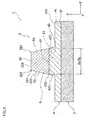
- Fig. 4 is an enlarged view of an IV portion of Fig. 2 .
- Fig. 5 is a cross sectional view in a short direction for description of a structure of a conductive portion in the embodiment of the invention.
- Fig. 6 is a cross sectional view in a longitudinal direction for description of the structure of the conductive portion in the embodiment of the invention.
- Fig. 7 is a diagram illustrating the conductive portion in the embodiment of the invention, and is a cross sectional view in a longitudinal direction for description of a method of obtaining a first approximate line of a contact surface of the conductive portion.
- a wiring board 1 in the present embodiment is used as an electrode substrate of a touch panel or a touch sensor, and includes a substrate 3 and a wiring body 2 in which a conductive portion 5 is supported by the substrate 3 through an adhesive layer 4 as illustrated Fig. 1 to Fig. 3 .
- the wiring body 2 of the present embodiment four straight line-shaped conductive portions 5 are provided substantially in parallel on the substrate 3.
- the invention is not particularly restricted thereto.
- Use of the wiring board 1 is not particularly restricted.
- the "wiring body 2" in the present embodiment corresponds to an example of a “wiring body” in the invention
- the "substrate 3" in the present embodiment corresponds to an example of a “support” in the invention
- the "adhesive layer 4" the present embodiment corresponds to an example of a “resin layer”
- the "conductive portion 5" in the present embodiment corresponds to an example of a "conductive portion” in the invention.
- the substrate 3 is made of an insulating film having flexibility.
- a material included in the insulating film may include polyethylene terephthalate (PET), polyethylene naphthalate (PEN), polyimide resin (PI), polyetherimide resin (PEI), polycarbonate (PC), polyether ether ketone (PEEK), liquid crystal polymer (LCP), cycloolefin polymer (COP), silicone resin (SI), acrylic resin, phenol resin, epoxy resin, green sheet, glass, etc.
- An easily adhesive layer or an optical adjustment layer may be formed in the substrate 3.
- transparent materials are selected as materials included in the substrate 3 and the adhesive layer 4, respectively.
- the adhesive layer 4 serving as a resin layer in the present embodiment is a member bonding and fixing the substrate 3 and the conductive portion 5 to each other.
- a material included in the adhesive layer 4 may include a UV-curing resin, a thermosetting resin, or a thermoplastic resin such as epoxy resin, acrylic resin, polyester resin, urethane resin, vinyl resin, silicone resin, phenol resin, polyimide resin, etc. or ceramic.
- the adhesive layer 4 in the present embodiment includes a smooth portion 41 provided on a main surface 31 of the substrate 3 and having a substantially constant thickness, and a protrusion 42 formed on the smooth portion 41.
- the "smooth portion 41" in the present embodiment corresponds to an example of a "flat portion” in the invention
- the "protrusion 42" in the present embodiment corresponds to an example of a "protrusion” in the invention.
- the smooth portion 41 is uniformly provided to cover the main surface 31 of the substrate 3, and a main surface 411 of the smooth portion 41 is a surface substantially parallel to the main surface 31 of the substrate 3.
- the main surface 31 of the substrate 3 is a surface substantially parallel to a Y direction of Fig. 1 to Fig. 3 .
- the protrusion 42 is formed between the smooth portion 41 and the conductive portion 5, and provided to protrude in a direction away from the substrate 3 (+Z direction of Fig. 1 ). For this reason, a thickness (height) of the adhesive layer 4 in a portion in which the protrusion 42 is provided is larger than a thickness (height) of the adhesive layer 4 in the smooth portion 41.
- the protrusion 42 includes two side surfaces 421 and 421, which have straight line shapes in a section view in a short direction and are inclined to be separated from each other as being separated from a contact surface 43 (described below).
- a thickness (height) of the smooth portion 41 refers to a distance from a surface of the adhesive layer 4 facing the main surface 31 of the substrate 3 to the main surface 411 in the Z direction (direction in which the adhesive layer 4 and the conductive portion 5 are stacked).
- a thickness (height) of the protrusion 42 refers to a distance from a portion in which the smooth portion 41 and the protrusion 42 are connected to each other (that is, the same plane as the main surface 411) to the contact surface 43 in the Z direction (direction in which the adhesive layer 4 and the conductive portion 5 are stacked).
- a thickness (height) of the adhesive layer 4 in a portion in which the protrusion 42 is provided refers to a sum of the thickness (height) of the smooth portion 41 and the thickness (height) of the protrusion 42.
- the thickness (height) of the smooth portion 41 is preferably within a range of 5 ⁇ m to 2,000 ⁇ m
- the thickness (height) of the protrusion 42 is preferably within a range of 0.65 ⁇ m to 33 ⁇ m
- a minimum thickness (height) of the protrusion 42 is preferably within a range of 0.35 ⁇ m to 17 ⁇ m.
- a maximum thickness (height) of the protrusion 42 refers to a thickness of the protrusion 42 in a portion corresponding to a concave portion 511 (described below) of a contact surface 51 (described below) of the conductive portion 5.
- the minimum thickness (height) of the protrusion 42 refers to a thickness of the protrusion 42 in a portion corresponding to a convex portion 512 (described below) of the contact surface 51 of the conductive portion 5.
- the adhesive layer 4 of the present embodiment comes into contact with the conductive portion 5 (specifically, the contact surface 51) on the contact surface 43.
- the contact surface 43 in response to the contact surface 51 of the conductive portion 5 having a concave-convex surface (details are described below) in a section view in a longitudinal direction, the contact surface 43 includes a concave-convex surface complementary to the concave-convex shape of the contact surface 51.
- the contact surface 43 is connected to the side surfaces 421 and 421 of the protrusion 42 at both ends thereof in the section view in the short direction.
- minute concave and convex portions are formed on the contact surface 43 in a cross section in the short direction when compared to a concavo-convex shape of the contact surface 43 in a cross section in a longitudinal direction.
- a concavo-convex shape of the contact surface 43 in the cross section in the short direction is formed based on surface roughness of the contact surface 51 of the conductive portion 5. The surface roughness of the contact surface 51 will be described below in detail.
- a concavo-convex shape at a boundary between the protrusion 42 and the conductive portion 5 in the cross section in the short direction is exaggeratingly illustrated to describe the wiring body 2 in the present embodiment in an easily understood manner.
- the conductive portion 5 is stacked on the protrusion 42 of the adhesive layer 4, and formed to protrude in the +Z direction in Fig. 1 to Fig. 3 .
- the conductive portion 5 includes a conductive particle CP and a binder resin BD.
- conductive particles CP is substantially evenly dispersed in the binder resin BD, and conductivity is assigned to the conductive portion 5 when conductive particles CP come into contact with each other.
- some of the conductive particles CP are exposed from the binder resin BD.
- the invention is not restricted thereto.
- the conductive particles CP may not be exposed from the binder resin BD. Incidentally, in Fig.
- the conductive particles CP fill the conductive portion 5 to have a gap between conductive particles CP for convenience of description.
- the conductive particles CP densely fill the conductive portion 5 when compared to description in Fig. 4 .
- the conductive portion 5 is formed by applying and hardening conductive paste.
- the conductive paste may include conductive paste configured by mixing the conductive particles CP with the binder resin BD, water or a solvent, and various addition agents.
- Specific examples of the conductive particles CP may include conductive powder or metal salt.
- the conductive powder may include a metal material such as silver, copper, nickel, tin, bismuth, zinc, indium, palladium, etc., or a carbon-based material such as graphite, carbon black (furnace black, acetylene black, Ketjen black), carbon nanotube, carbon nanofiber, etc.
- the metal salt may include salt of these metals.
- a conductive particle having a particle diameter D within a range of 0.01 ⁇ m to 2 ⁇ m (0.01 ⁇ D ⁇ 2) depending on a width of the formed conductive portion 5 may be used as a conductive particle CP contained in the conductive portion 5. It is preferable to use conductive particles having an average diameter ⁇ which is half or less the width of the formed conductive portion 5 in terms of stabilizing electrical resistivity in the conductive portion 5.
- the carbon-based material is used as the conductive particle CP, it is preferable to use a particle, whose specific surface area measured by a BET method is 20 m 2 /g or more.
- the particle diameter D of the conductive particle CP is a general term for particle diameters D 1 to D 4 described below.
- the metal material is preferably used as the conductive particle CP.
- the carbon-based material is preferably used as the conductive particle CP. Using the carbon-based material as the conductive particle is preferable in terms of improving haze or total light reflectance of a mesh film.
- binder resin BD may include acrylic resin, polyester resin, epoxy resin, vinyl resin, urethane resin, phenol resin, polyimide resin, silicone resin, fluoride resin, etc.
- solvent may include ⁇ -terpineol, butyl carbitol acetate, butyl carbitol, 1-decanol, butyl cellosolve, diethylene glycol monoethyl ether acetate, tetradecane, etc.
- the binder resin may be omitted from the material included in the conductive portion 5.
- a width (maximum width) S 6 , S 8 of the conductive portion 5 is preferably within a range of 50 nm to 1,000 ⁇ m, more preferably within a range of 500 nm to 150 ⁇ m, even more preferably within a range of 1 ⁇ m to 10 ⁇ m, and further even more preferably within a range of 1 ⁇ m to 5 ⁇ m.
- a thickness of the conductive portion 5 is preferably within a range of 50 nm to 3,000 ⁇ m, more preferably within a range of 500 nm to 450 ⁇ m, and even more preferably within a range of 500 nm to 10 ⁇ m.
- an external shape of the conductive portion 5 of the present embodiment includes the contact surface 51, a top surface 52, and two side surfaces 53 and 53.
- the contact surface 51 has concave portions 511 and convex portions 512 in the section view in the longitudinal direction, and is set to a surface having a concave-convex shape.
- the contact surface 51 is continuously formed between the side surfaces 53 and 53 in the section view in the short direction.
- the contact surface 51 is set to a surface having a concave-convex shape including minute concave and convex portions in the cross section in the short direction when compared to the concave and convex portions 511 and 512 formed in the cross section in the longitudinal direction.
- the contact surface 51 is positioned on the top surface 52 side with respect to the main surface 411 of the smooth portion 41 in the Z direction.
- the minute concave and convex portions of the contact surface 51 are included inside the protrusion 42 of the adhesive layer 4, and thus do not corrode the smooth portion 41 of the adhesive layer 4. For this reason, durability the resin layer 4 is improved.
- the "contact surface 51" in the present embodiment corresponds to an example of a "first surface” in the invention.
- the top surface 52 facing the contact surface is substantially parallel to the main surface 31 of the substrate 3.
- the top surface 52 is continuously formed through corner portions 521 and 521 between the side surfaces 53 and 53 in the section view in the short direction.
- the corner portions 521 and 521 preferably correspond to 90° to 170° (90° ⁇ ⁇ ⁇ 170°), and more preferably correspond to 90° to 120° (90° ⁇ ⁇ ⁇ 120°) in terms of suppressing diffused reflection of light on the side surface 53.
- an angle of the corner portion 521 between one side surface 53 and the top surface 52 is substantially equal to an angle of the corner portion 521 between the other side surface 53 and the top surface 52.
- a range between the corner portions 521 and 521 corresponds to an example of a "second surface” in the invention.
- burr shapes are formed at portions corresponding to the corner portions 521 and 521, respectively, a range between the burr shapes corresponds to an example of the "second surface” in the invention.
- R shapes are formed at the portions corresponding to the corner portions 521 and 521, respectively, a range between positions at which radii of curvatures of the R shapes correspond to minimum values or a range between central positions in a section view of the R shapes corresponds to an example of the "second surface" in the invention.
- inclined angles of the respective side surfaces 421 and 421 are substantially equal to each other.
- the invention is not particularly restricted thereto, and the inclined angles of the respective side surfaces 421 and 421 may set to different inclined angles.
- inclined angles of the respective side surfaces 53 and 53 are substantially equal to each other.
- the invention is not particularly restricted thereto, and the inclined angles of the respective side surfaces 53 and 53 may set to different inclined angles.
- the inclined angle of the side surface 53 is substantially equal to the inclined angle of the side surface 421.
- the top surface 52 includes a flat portion 523 in a cross section of the conductive portion 5 in a short direction.
- the flat portion 523 is a straight line-shaped portion (that is, a portion having an extremely large radius of curvature) present on the top surface 52 in the cross section of the conductive portion 5 in the short direction, and has flatness of 0.5 ⁇ m or less.
- the flatness may be measured by the JIS method (JIS B0621 (1984)).
- the flatness of the flat portion 523 is obtained using a non-contact measurement scheme using laser light.
- a measuring object for example, the top surface 52 or the side surface 53
- an image of reflected light thereof is formed on an image pick-up device (for example, a two-dimensional (2D) CMOS) to measure the flatness.
- a scheme maximum deflection-type flatness
- a scheme of measuring or calculating the flatness is not particularly restricted to the above-described schemes.
- a scheme of measuring the flatness may correspond to a contact-type measurement scheme using a dial gauge, etc.
- a scheme maximum tilt-type flatness
- a scheme may be used as a scheme of calculating the flatness to calculate a value of a gap, which is generated when a target plane is interposed between parallel planes, as the flatness.
- the flat portion 523 of the present embodiment is formed on the substantially whole top surface 52.
- the invention is not particularly restricted to the above description, and the flat portion may be formed in a portion of the top surface. In this case, for example, the flat portion may be formed in a region not including both ends of the top surface.
- a width of the flat portion is at least half or more a width of the top surface.
- the side surfaces 53 and 53 have straight line shapes in the section view in the short direction, and are formed to be inclined such that the side surfaces 53 and 53 approach each other (have a so-called tapered shape) as being separated from the contact surface 51.
- the side surfaces 53 and 53 join the side surfaces 421 and 421 at portions connected to the contact surface 51 (or the contact surface 43) in the section view in the short direction.
- the side surface 53 of the conductive portion 5 and the side surface 421 of the protrusion 42 in the adhesive layer 4 form one plane by being smoothly continued.
- the side surface 421 of the protrusion 42 preferably has a shape in which a hem of the protrusion 42 does not widen in a cross section of the conductive portion 5 in a width direction.
- the side surface 421 preferably has a shape in which the side surface 421 is not recessed from a virtual straight line passing through a portion at which the side surface 421 is connected to the side surface 53 and a portion at which the side surface 421 is connected to the smooth portion 41.
- the side surface 53 is positioned between the contact surface 51 and the top surface 52.
- the side surface 53 is connected to the top surface 52 at a first portion 531, and connected to the contact surface 51 at a second portion 532.
- the first portion 531 is identical to the corner portion 521.
- the conductive portion 5 of the present embodiment has a tapered shape, in which a width is narrowed as being separated from the adhesive layer 4, and thus the second portion 532 is positioned outside the first portion 531.
- the side surface 53 of the present embodiment is a surface having a straight line shape extending on a virtual straight line (not illustrated) passing through the first and second portions 531 and 532 in the cross section of the conductive portion 5 in the short direction.
- the shape of the side surface 53 is not particularly restricted to the above-described shape.
- the side surface 53 may protrude outward from the virtual straight line passing through the first and second portions 531 and 532 in the cross section of the conductive portion 5 in the short direction.
- the side surface 53 preferably has a shape which is not recessed inward from the virtual straight line passing through the first and second portions (a shape in which a hem of the conductive portion does not widen) in the cross section of the conductive portion 5 in the short direction.
- the side surface 53 includes a flat portion 533 in the cross section of the conductive portion 5 in the width direction.
- the flat portion 533 is a portion having a straight line shape (that is, a portion having an extremely large radius of curvature) present on the side surface 53 in the cross section of the conductive portion 5 in the short direction, and has flatness of 0.5 ⁇ m or less.
- a portion of the side surface 53 extending to substantially match the virtual straight line is included in the flat portion 533.
- the flat portion 533 is formed substantially on the whole side surface 53.
- the invention is not particularly restricted to the above description, and the flat portion may be formed in a portion of the side surface.
- a surface roughness of the contact surface 51 of the conductive portion 5 in the present embodiment is preferably rougher than a surface roughness of the top surface 52 of the conductive portion 5 in terms of strongly fixing the conductive portion 5 to the adhesive layer 4.
- the top surface 52 includes the flat portion 523, and thus the above-described relative relation with regard to surface roughness in the conductive portion 5 (a relation in which the surface roughness of the contact surface 51 is relatively rougher than the surface roughness of the top surface 52).
- the surface roughness Ra of the contact surface 51 of the conductive portion 5 is within a range of about 0.1 ⁇ m to 3 ⁇ m, and the surface roughness Ra of the top surface 52 is within a range of about 0.001 ⁇ m to 1.0 ⁇ m.
- the surface roughness Ra of the contact surface 51 of the conductive portion 5 is more preferably within a range of 0.1 ⁇ m to 0.5 ⁇ m, and the surface roughness Ra of the top surface 52 is more preferably within a range of 0.001 ⁇ m to 0.3 ⁇ m.
- a ratio of the surface roughness of the top surface 52 to the surface roughness of the contact surface 51 preferably corresponds to 0.01 or more and less than 1, and more preferably corresponds to 0.1 or more and less than 1.
- the surface roughness of the top surface 52 is preferably 1/5 or less the width (maximum width) of the conductive portion 5. Such surface roughness may be measured by the JIS method (JIS B0601 (revised on March 21, 2013)).
- the "surface roughness Ra” herein refers to an “arithmetic average roughness Ra”.
- This "arithmetic average roughness Ra” refers to a roughness parameter obtained by excluding a long wavelength component (waviness component) from a profile curve. The waviness component is separated from the profile curve based on a measurement condition (for example, dimensions of an object, etc.) necessary to obtain a form.
- the side surface 53 includes the flat portion 533.
- the surface roughness of the contact surface 51 is relatively rougher than the surface roughness of the side surface 53 including the flat portion 533.
- the surface roughness Ra of the contact surface 51 is within a range of 0.001 ⁇ m to 1.0 ⁇ m.
- the surface roughness Ra of the side surface 53 is preferably within a range of 0.001 ⁇ m to 0.3 ⁇ m.
- the top surface 52 includes the flat portion 523
- the side surface 53 includes the flat portion 533.
- a diffuse reflectance of the wiring body 2 on a side of surfaces except for contact surface 51 is preferably relatively smaller than a diffuse reflectance of the wiring body 2 on a side of the contact surface 51.
- a ratio of the diffuse reflectance of the wiring body 2 on the side of the surfaces except for the contact surface 51 to the diffuse reflectance of the wiring body 2 on the side of the contact surface 51 is preferably 0.1 or more and less than 1, and more preferably 0.3 or more and less than 1.
- the conductive portion 5B illustrated in Fig. 5 includes a conductive particle CPa and a binder resin BDa.
- some of conductive particles CPa protrude from the binder resin BDa on a contact surface 51B.
- the contact surface 51B has a concavo-convex shape.
- the binder resin BDa penetrates between conductive particles CPa, and the binder resin BDa covers the conductive particles CPa on a top surface 52B and a side surface 53B.
- a flat portion 523B is formed on the top surface 52B.
- a flat portion 533B is formed on the side surface 53B.
- L 1 denotes a unit length of the contact surface 51 in the section view in the longitudinal direction
- L 2 denotes a unit length of the top surface 52 in the section view in the longitudinal direction.
- the unit length of the contact surface 51 and the unit length of the top surface 52 are obtained as below.
- an arbitrary reference surface and a unit region W are set as illustrated in Fig. 7 .
- the arbitrary reference surface is set to the main surface 411 of the smooth portion 41.
- the unit region W is set to a region having a width, a length of which corresponds to the unit length of the contact surface 51, in the cross section in the longitudinal direction. Further, within the unit region W, positions based on the reference surface are obtained with respect to arbitrary measurement positions (ten positions of P1 to P10 in the present embodiment) on the contact surface 51.
- a first approximate line 513 of the contact surface 51 is calculated by an approximation method based on an obtained value.
- a length of the first approximate line 513 in the section view in the longitudinal direction in the unit region W is set to the unit length of the contact surface 51.
- Specific examples of the approximation method may include a polynomial approximation method using a least squares method.
- a position based on the reference surface is obtained at an arbitrary measurement position on the top surface 52 within the unit region W.
- a second approximate line 522 of the top surface 52 is calculated by an approximation method such as polynomial approximation based on an obtained value.
- a length of the second approximate line 522 in the section view in the longitudinal direction in the unit region W is set to the unit length of the top surface 52.
- a gap between adjacent measurement positions is set to three times or more an average particle diameter of the conductive particles CP.
- the average particle diameter of the conductive particles CP is obtained using a scanning electron microscope (SEM) or a transmission electron microscope (TEM). Specifically, an arithmetic mean value of particle diameters of a plurality of (at least 100) conductive particles CP measured by the SEM or the TEM is set to the average particle diameter of the conductive particles CP.
- SEM scanning electron microscope
- TEM transmission electron microscope
- a side (or a diameter) in a longitudinal direction is measured as the particle diameter of the conductive particle CP.
- conductive particles CP when the average particle diameter of the conductive particles CP is obtained, conductive particles CP whose particle diameters (that is, sides in the longitudinal direction in the particle diameters of the conductive particles CP) are less than 100 nm are excluded from the measuring object ( ⁇ ⁇ 100 nm).
- conductive particles CP in an aggregate state or conductive particles CP having distorted external shapes are excluded from the measuring object.
- examples of the conductive particles CP in the aggregate state may include conductive particles CP adhering to each other to have a flake shape.
- the concave portion 511 of the present embodiment is a portion on the contact surface 51 corresponding to a an inflection point 513a at which a gradient of a curve is changed from a positive value to a negative value in the above-described first approximate line 513 in the cross section in the longitudinal direction (see Fig. 7 ).
- the convex portion 512 is a portion on the contact surface 51 corresponding to a an inflection point 513b at which the gradient of the curve is changed from a negative value to a positive value in the above-described first approximate line 513 in the cross section in the longitudinal direction (see Fig. 7 ).
- the unit length L 1 of the contact surface 51 is preferably within a range of 20.1 ⁇ m to 30 ⁇ m
- the unit length L 2 of the top surface 52 is preferably within a range of 20 ⁇ m to 21 ⁇ m.
- a ratio of the unit length L 1 of the contact surface 51 to the unit length L 2 of the top surface 52 is preferably within a range of 1.01 to 1.43, and more preferably within a range of 1.05 to 1.30.
- Formula (6) is satisfied in terms of improving a mechanical joining force between the adhesive layer 4 and the conductive portion 5, and preventing damage to the conductive portion 5.
- S 1 denotes an average gap between the contact surface 51 and the top surface 52 in the concave portion 511
- S 2 denotes an average gap between the contact surface 51 and the top surface 52 in the convex portion 512.
- the average gap between the contact surface 51 and the top surface 52 in the concave portion 511 is obtained as below. That is, a gap between the inflection point 513a and a projection point 522a obtained by projecting the inflection point 513a onto the second approximate line 522 along the Z direction is obtained at a plurality of (at least ten) positions, and an arithmetic mean value of obtained gaps between the contact surface 51 and the top surface 52 in the concave portion 511 is set to the average gap between the contact surface 51 and the top surface 52 in the concave portion 511.
- the average gap between the contact surface 51 and the top surface 52 in the convex portion 512 is obtained as below. That is, a gap between the inflection point 513b and a projection point 522b obtained by projecting the inflection point 513b onto the second approximate line 522 along the Z direction is obtained at a plurality of (at least ten) positions, and an arithmetic mean value of obtained gaps between the contact surface 51 and the top surface 52 in the convex portion 512 is set to the average gap between the contact surface 51 and the top surface 52 in the convex portion 512.
- the average gap between the contact surface 51 and the top surface 52 may not be obtained using the above-described scheme.
- gaps between the contact surface 51 and the top surface 52 in the concave portion 511 (or the convex portion 512) at ten or more positions may be measured using the SEM or the TEM, and an arithmetic mean value of obtained gaps between the contact surface 51 and the top surface 52 may be set to the average gap between the contact surface 51 and the top surface 52 in the concave portion 511 (or the convex portion 512).
- the gap between the contact surface 51 and the top surface 52 in the concave portion 511 and the gap between the contact surface 51 and the top surface 52 in the convex portion 512 are regarded as substantially constant thicknesses in the section view of the conductive portion 5 in the short direction when compared to the concave and convex portions in the cross section of the conductive portion 5 in the longitudinal direction despite an influence of the minute concave and convex portions in the cross section of the conductive portion 5 in the short direction.
- An average gap S 1 between the contact surface 51 and the top surface 52 in the concave portion 511 is preferably within a range of 0.35 ⁇ m to 17 ⁇ m.
- an average gap S 2 between the contact surface 51 and the top surface 52 in the convex portion 512 is preferably within a range of 0.65 ⁇ m to 33 ⁇ m.
- An average between S 1 and S 2 may be used as the height (average height) of the conductive portion 5.
- a ratio of the thickness (height) of the protrusion 42 to the height of the conductive portion 5 is preferably within a range of 0.67 to 1.5.
- Formula (7) below is preferably satisfied in terms of further improving the mechanical joining force between the adhesive layer 4 and the conductive portion 5.
- S 5 denotes an average height difference between the concave portion 511 and the convex portion 512
- D 4 denotes an average particle diameter of the conductive particles CP.
- the average height difference between the concave portion 511 and the convex portion 512 is obtained as below. That is, a value obtained by subtracting the average gap between the contact surface 51 and the top surface 52 in the concave portion 511 from the average gap between the contact surface 51 and the top surface 52 in the convex portion 512 obtained as described above is set to the average height difference between the concave portion 511 and the convex portion 512.
- the average height difference between the concave portion 511 and the convex portion 512 may not be obtained using the above-described scheme.
- gaps between the contact surface 51 and the top surface 52 in the concave portion 511 at ten or more positions and gaps between the contact surface 51 and the top surface 52 in the convex portion 512 at ten or more positions may be measured using the SEM or the TEM, and a value obtained by subtracting an arithmetic mean value of the measured gaps between the contact surface 51 and the top surface 52 in the concave portion 511 from an arithmetic mean value of the measured gaps between the contact surface 51 and the top surface 52 in the convex portion 512 may be set to the average height difference between the concave portion 511 and the convex portion 512.
- the average height difference S 5 between the concave portion 511 and the convex portion 512 is preferably within a range of 0.3 ⁇ m to 17 ⁇ m.
- the contact surface 51 includedes a waveform in which the concave portion 511 and the convex portion 512 are alternately continued, and Formula (8) below is satisfied.
- S 3 denotes an average gap between adjacent convex portions 512
- D 1 denotes the average particle diameter of the conductive particles CP.
- the average gap between the adjacent convex portions 512 is obtained as below. That is, a gap between two adjacent inflection points 513b is obtained at positions, and an arithmetic mean value of obtained gaps between inflection points 513b is set to the average gap between the adjacent convex portions 512. In this case, the gap between the two adjacent inflection points 513b is measured at least at ten (that is, eleven inflection points 513b are present) or more positions.
- the average gap between the adjacent convex portions 512 may not be obtained using the above-described scheme.
- a gap between adjacent convex portions 512 may be measured at ten or more positions using the SEM or the TEM, and an arithmetic mean value of measured gaps between adjacent convex portions 512 may be set to the average gap between the adjacent convex portions 512.
- the average gap S 3 between the adjacent convex portions 512 is preferably within a range of 3 ⁇ m to 20 ⁇ m.
- Formula (9) below is satisfied in terms of more reliably ensuring conductivity along an extending direction of the conductive portion 5.
- Formula (10) below is more preferably satisfied (with regard to S 6 , see Fig. 3 ).
- S 4 denotes the average gap between the contact surface 51 and the top surface 52 in the concave portion 511
- D 2 denotes the average particle diameter of the conductive particles CP.
- S 6 denotes a maximum width of the conductive portion 5 in the section view in the short direction
- D 4 denotes the average particle diameter of the conductive particles CP.
- the maximum width of the conductive portion 5 in the section view in the short direction is obtained as below. That is, a maximum width of the conductive portion 5 is measured at ten or more positions in the cross section in the short direction using the SEM or the TEM, and an arithmetic mean value of measured maximum widths of the conductive portion 5 is set to the maximum width of the conductive portion 5.
- the average gap S 4 between the contact surface 51 and the top surface 52 in the concave portion 511 is preferably set within the same range as that of the above-described S 1 .
- Formula (11) below is preferably satisfied in terms of further improving the mechanical joining force between the adhesive layer 4 and the conductive portion 5.
- S 7 denotes an average gap between adjacent convex portions 512
- S 8 denotes the maximum width of the conductive portion 5 in the section view in the short direction.
- the average gap S 7 between the adjacent convex portions 512 is preferably set within the same range as that of the above-described S 3 .
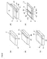
- Fig. 8(a) to Fig. 8(e) are cross-sectional views for description of the method of manufacturing the wiring board 1 in the present embodiment.
- intaglio 6 in which a recessed portion 61 having a shape corresponding to the conductive portion 5 is prepared.
- a material included in the intaglio 6 may include nickel, silicon, silicon dioxide, organic silica, glassy carbon, a thermoplastic resin, a light curing resin, etc.
- a width of the recessed portion 61 is preferably within a range of 50 nm to 1,000 ⁇ m, more preferably within a range of 500 nm to 150 ⁇ m, even more preferably within a range of 1 ⁇ m to 10 ⁇ m, and further even more preferably within a range of 1 ⁇ m to 5 ⁇ m.
- a depth of the recessed portion 61 is preferably within a range of 50 nm to 3,000 ⁇ m, more preferably within a range of 500 nm to 450 ⁇ m, and even more preferably within a range of 500 nm to 10 ⁇ m.
- a release layer made of a graphite-based material, a silicone-based material, a fluorine-based material, a ceramic-based material, an aluminum-based material, etc. is preferably formed on a surface of the intaglio 6 including the recessed portion 61 to improve a release property.
- the recessed portion 61 of the intaglio 6 is filled with an electrically conductive material 7.
- the above-described conductive paste is used as the electrically conductive material 7.
- Examples of a method of filling the recessed portion 61 of the intaglio 6 with the electrically conductive material 7 may include a dispensing method, an ink-jet method, screen printing, etc. Otherwise, the examples may include a method in which after coating using a slit coating method, a bar coating method, a blade coating method, a dip coating method, a spray coating method, or a spin coating method, the electrically conductive material coating a portion other than the concave portion is removed by wiping, scraping, sucking, sticking, washing, or blowing.
- a composition, etc. of the electrically conductive material may be appropriately used properly according to a shape of the intaglio, etc.
- the conductive portion 5 is formed by heating the electrically conductive material 7 that fills the recessed portion 61 of the intaglio 6.
- a condition for heating the electrically conductive material 7 may be appropriately set depending on the composition of the electrically conductive material 7, etc.
- a mold (not illustrated) having a concave-convex shape in a longitudinal direction is pressed against the electrically conductive material 7 filling the recessed portion 61 to heat the electrically conductive material 7. Otherwise, content of water or solvent contained in the electrically conductive material 7 is adjusted such that an upper surface of the electrically conductive material 7 has a concave-convex shape after the electrically conductive material 7 is heated.
- the electrically conductive material 7 contracts in volume through the heating treatment.
- an external surface of the electrically conductive material 7 except for the upper surface is formed in a shape along the recessed portion 61.
- a surface having a concave-convex shape (that is, the contact surface 51) is formed on an upper surface of the conductive portion 5.
- a void 62 connected to an external space of the recessed portion 61 is formed on the conductive portion 5 inside the recessed portion 61 of the intaglio 6.
- a method of processing the electrically conductive material 7 is not restricted to heating.
- the electrically conductive material 7 may be irradiated with an energy ray such as an infrared ray, an ultraviolet ray, laser light, etc. or may only be dried.
- a resin material 8 for forming the adhesive layer 4 is applied onto the intaglio 6.
- the resin material 8 may include the same material as the above-mentioned material included in the adhesive layer 4.
- Examples of a method of applying the resin material 8 onto the intaglio 6 may include screen printing, a spray coating method, a bar coating method, a dip method, an ink-jet method, etc. Through this application, the resin material 8 penetrates into the recessed portion 61 including the concave-convex shape of the contact surface 51.
- a substrate is disposed from above the resin material 8 applied onto the intaglio 6. This disposition is preferably performed in a vacuum in order to inhibit a bubble from penetrating between the resin material 8 and the substrate 3.
- the resin material 8 is hardened. Examples of a method of hardening the resin material 8 may include irradiation with an energy ray such as an infrared ray, an ultraviolet ray, laser light, etc., heating, annealing, drying, etc.
- an energy ray such as an infrared ray, an ultraviolet ray, laser light, etc., heating, annealing, drying, etc.
- the adhesive layer 4 is formed, and the substrate 3 and the conductive portion 5 are bonded and fixed to each other through the adhesive layer 4.
- the protrusion 42 of the adhesive layer 4 is formed.
- the substrate 3 is stacked after the resin material 8 is applied onto the intaglio 6.
- the invention is not particularly restricted thereto.
- the substrate 3 may be stacked on the intaglio 6 through the resin material 8 by disposing the substrate 3, in which the resin material 8 is applied onto the main surface (surface facing the intaglio 6) of the substrate 3 in advance, on the intaglio 6.
- the substrate 3, the adhesive layer 4, and the conductive portion 5 may be released from a mold, thereby obtaining the wiring board 1 (see Fig. 8(e) ).
- a mold release operation may be facilitated.
- the wiring body 2 and the wiring board 1 in the present embodiment accomplish the following effects.
- the contact surface 51 in the section view in the longitudinal direction, is set to a surface having a concave-convex shape, and Formula (12) below is satisfied.
- Formula (12) below is satisfied.
- the mechanical joining force between the conductive portion 5 and the adhesive layer 4 is improved, and separation between the conductive portion 5 and the adhesive layer 4 is suppressed.
- the contact surfaces 51 and 43 between the conductive portion 5 and the adhesive layer 4 are set to surfaces having concave-convex shapes, adhesion between the conductive portion 5 and the adhesive layer 4 is improved due to an anchoring effect.
- a contact area between the conductive portion 5 and the adhesive layer 4 increases, and the conductive portion 5 and the adhesive layer 4 may be strongly bonded to each other.
- adhesion (bond strength) between the conductive portion 5 and the adhesive layer 4 in the wiring body 2 of the present embodiment is preferably 10 N/cm or more.
- L 1 denotes a unit length of the contact surface 51 in the section view in the longitudinal direction
- L 2 denotes a unit length of the top surface 52 in the section view in the longitudinal direction.
- the adhesive layer 4 serving as a resin layer has the smooth portion 41 and the protrusion 42.
- the protrusion 42 protrudes from the main surface 411 of the smooth portion 41 toward the conductive portion 5 side to correspond to a portion supporting the conductive portion 5. Further, when the protrusion 42 comes into contact with the conductive portion 5, the contact surface 51 of the conductive portion 5 is positioned on a side of the top surface 52 of the conductive portion 5 with respect to the main surface 411 of the smooth portion 41.
- the adhesive layer 4 in the portion supporting the conductive portion 5 is formed to be thicker by a thickness of the protrusion 42, rigidity of the adhesive layer 4 in the portion supporting the conductive portion 5 is improved, and thus separation between the conductive portion 5 and the adhesive layer 4 may be suppressed.
- the contact surface 51 of the conductive portion 5 is positioned on the side of the top surface 52 of the conductive portion 5 with respect to the main surface 411 of the smooth portion 41, the concave and convex portions of the contact surface 51 are included inside the protrusion 42.
- the smooth portion 41 is not corroded by the conductive portion 5, and a substantially constant thickness may be maintained. In this way, a thin-walled portion is not generated in the smooth portion 41, and thus durability of the adhesive layer 4 may be improved.
- the main surface 411 of the smooth portion 41 is formed to be substantially flat. In this way, it is possible to improve an adhesive property between the adhesive layer 4 and the conductive portion 5, and to prevent light entering the wiring body 2 from the outside from being irregularly reflected on the main surface 411 of the smooth portion 41. That is, the wiring body 2 of the present embodiment may suppress separation between the adhesive layer 4 and the conductive portion 5, and improve visibility.
- the conductive portion 5 may be inhibited from remaining inside the recessed portion 61 of the intaglio 6 at the time of mold release when the wiring board 1 is manufactured. In addition, with the improvement in the release property, the conductive portion 5 may be thinned.
- Formula (13) below is satisfied in terms of improving the mechanical joining force between the adhesive layer 4 and the conductive portion 5, and preventing damage to the conductive portion 5. That is, in a range less than a lower limit of Formula (13) below, the convex portion 512 becomes sharp, and the conductive portion 5 is damaged in the convex portion 512. Furthermore, there is a concern that separation between the adhesive layer 4 and the conductive portion 5 may occur. In addition, when the value is equal to an upper limit of Formula (13) below, the contact surface 51 is regarded as a surface having a concave-convex shape. Thus, there is a concern that the mechanical joining force between the adhesive layer and the conductive portion may not be improved, and separation between the adhesive layer and the conductive portion may occur. S 2 > S 1 ⁇ 0.5 S 2
- S 1 denotes an average gap between the contact surface 51 and the top surface 52 in the concave portion 511
- S 2 denotes an average gap between the contact surface 51 and the top surface 52 in the convex portion 512.
- the contact surface 51 of the present embodiment includes a waveform in which the concave portion 511 and the convex portion 512 are alternately continued, and Formula (14) below is satisfied.
- the mechanical joining force between the conductive portion 5 and the adhesive layer 4 is further improved, and separation between the conductive portion 5 and the adhesive layer 4 is suppressed.
- the contact surface 51 has a waveform in which the concave portion 511 and the convex portion 512 are periodically formed, stress is inhibited from being concentrated on a portion of the convex portion 512, and thus the convex portion 512 is inhibited from being damaged. In this way, separation between the conductive portion 5 and the adhesive layer 4 may be further inhibited from occurring.
- S 3 denotes an average gap between adjacent convex portions 512
- D 1 denotes the average particle diameter of the conductive particles CP.
- S 4 denotes the average gap between the contact surface 51 and the top surface 52 in the concave portion 511
- D 2 denotes the average particle diameter of the conductive particles CP.
- the side surfaces 53 and 53 have straight line shapes in the section view in the short direction, and are formed to be inclined such that the side surfaces 53 and 53 approach each other as being separated from the contact surface 51. In this way, a mold release operation may be facilitated when the substrate 3, the adhesive layer 4, and the conductive portion 5 are released from the intaglio 6.
- a focus is on a relative relation between surface roughness (that is, a roughness parameter obtained by excluding a wavelength component) of the contact surface 51 of the conductive portion 5 and surface roughness of a surface of the conductive portion 5 except for the contact surface 51 (a surface including the top surface 52 and the side surface 53) in the section view in the short direction.
- the surface roughness Ra of the contact surface 51 is set to be relatively rougher than the surface roughness Ra of the other surface. For this reason, it is possible to suppress diffused reflection of light entering from the outside while strongly bonding the adhesive layer 4 and the conductive portion 5 together.
- the width of the conductive portion 5 is within a range of 1 ⁇ m to 5 ⁇ m, and when a relative relation between the surface roughness of the contact surface 51 and the surface roughness of the other surface satisfies the above-described relation, it is possible to noticeably accomplish the effect that diffused reflection of light entering from the outside may be suppressed while strongly bonding the adhesive layer 4 and the conductive portion 5 together.
- the side surface 53 extends to substantially match the virtual straight line passing through the first and second portions 531 and 532.
- the side surface does not have a shape recessed inward from the virtual straight line passing through the first and second portions 531 and 532 (a shape in which a hem of the conductor pattern widens) in the cross section of the conductive portion 5 in the short direction.
- a shape recessed inward from the virtual straight line passing through the first and second portions 531 and 532 a shape in which a hem of the conductor pattern widens
- a diffuse reflectance of the wiring body 2 on the other surface side is relatively smaller than a diffuse reflectance of the wiring body 2 on the contact surface 51 side.
- the diffuse reflectance of the wiring body 2 is small, it is possible to inhibit the conductive portion 5 from appearing white, and to suppress a decrease in contract in a region in which the conductive portion 5 may be visually recognized. In this way, it is possible to further improve visibility of the wiring body 2 of the present embodiment.
- a wiring body in which a conductive portion is formed on a resin layer was manufactured according to the above-described manufacturing method.
- a width of the conductive portion was set to 2 ⁇ m. Referring to the conductive portion, when a length of a unit region W in a longitudinal direction is set to 12.5 ⁇ m, a unit length L 1 of a contact surface was 14.9 ⁇ m, and a unit length L 2 of a top surface was 12.9 ⁇ m.
- an average gap S 1 , S 4 between the contact surface and the top surface in a concave portion was 1.4 ⁇ m, and an average gap S 2 between the contact surface and the top surface in a convex portion was 1.9 ⁇ m.
- an average gap S 3 between adjacent convex portions was 5.8 ⁇ m.
- An average particle diameter D of conductive particles was 0.3 ⁇ m.
- a relation between the unit length L 1 of the contact surface and the unit length L 2 of the top surface 52 satisfies the above Formula (12).
- a relation between the average gap S 1 between the contact surface and the top surface in the concave portion and the average gap S 2 between the contact surface and the top surface in the convex portion satisfies the above Formula (13).
- a relation between the average particle diameter D of conductive particles and the average gap S 3 between adjacent convex portions satisfies the above Formula (14).
- a relation between the average gap S 4 between the contact surface and the top surface in the concave portion and the average particle diameter D of conductive particles satisfies the above Formula (15).
- a Sia test was conducted on the wiring body to verify bond strength between the resin layer and the conductive portion in the wiring body.
- a Sia tool having a distal end diameter of 30 ⁇ m was used. This Sia tool was moved at 50 ⁇ m/S in parallel to a side surface of the conductive portion to obtain a force when the conductive portion was separated from the resin layer.
- the test was conducted on the wiring body at eight arbitrary positions using the above-described method, and an average of obtained forces was set to bond strength between the resin layer and the conductive portion. As a result of conducting the Sia test, bond strength between the resin layer and the conductive portion in the wiring body was 43 mN.
- EIAJ ED-4703 (Standards of Electronic Industries Association of Japan) determines that wire bond strength (bond strength) in a wire having a diameter of 0.018 mm used for a semiconductor device needs to be at least within a range of 15 mN to 30 mN.
- bond strength between the resin layer and the conductive portion in the wiring body is sufficiently large when compared to the necessary bond strength.
- JPCA-BM03 (Standards of Japan Electronics Packaging and Circuits Association) determines that peeling intensity of copper foil needs to be 3.5 N/cm or more.
- peeling intensity of copper foil obtained using a lamination process or a casting process substantially needs to be 10 N/cm or more.
- a value obtained by dividing the bond strength between the resin layer and the conductive portion in the wiring body by the distal end diameter of the Sia tool is 14 N/cm, the peeling intensity is sufficiently large when compared to the necessary peeling intensity. In this way, it has been found that a characteristic of the wiring body contributes to suppression of separation between the resin layer and the conductive portion.
- Fig. 9 is a plan view illustrating the touch sensor in the embodiment of the invention.
- Fig. 10 is an exploded perspective view illustrating the touch sensor in the embodiment of the invention.
- the touch sensor 10 of the present embodiment is a touch panel sensor corresponding to a projection-type capacitive sensing method.
- the touch sensor 10 is combined with a display device (not illustrated) and used as an input device having a function of detecting a touch position.
- a liquid crystal display, an organic electro luminescence (EL) display, electronic paper, etc. may be used as the display device without particular restriction.
- the touch sensor 10 includes a detection electrode and a driving electrode (an electrode 21 and an electrode 22 described below) disposed to face each other, and a predetermined voltage is periodically applied between the two electrodes from an external circuit (not illustrated).
- the touch sensor 10 for example, when a finger (external conductor) of an operator approaches the touch sensor 10, a capacitor (electrostatic capacity) is formed between the external conductor and the touch sensor, and an electrical state between the two electrodes changes.
- the touch sensor 10 may detect an operation position of the operator based on an electrical change between the two electrodes.
- the touch sensor 10 includes a wiring board that has a substrate 3, a first wiring body 2C, and a second wiring body 2D.
- the first wiring body 2C includes a resin layer 4C and a conductive layer 21.
- the conductive layer 21 includes detection electrodes 211, lead-out wires 212, and terminals 213.
- the number of electrodes 211 included in the first wiring body 2C is not particularly restricted, and may be arbitrarily set.
- the numbers of lead-out wires 212 and terminals 213 included in the first wiring body 2C are set depending on the number of electrodes 211.
- the respective electrodes 211 extend in a Y direction in the figure, and the electrodes 211 is arranged in an X direction in the figure.
- One ends of the lead-out wires 212 are connected to one ends of the electrodes 211 in a longitudinal direction, respectively.
- the terminals 213 electrically connected to an external circuit are connected to the other ends of the lead-out wires 212, respectively.
- the electrodes 211 have a mesh shape (net shape) including straight line-shaped conductive portions 5.
- a shape of each net including the conductive portion 5 is set to a substantially square shape.
- the shape of each net may correspond to geometric forms below. That is, the shape of the net may correspond to a triangle such as a regular triangle, an isosceles triangle, a right triangle, etc., and may correspond to a rectangle such as a parallelogram, a trapezoid, etc.
- the shape of the net may correspond to an n-polygon such as a hexagon, an octagon, a dodecagon, an icosagon, etc., a circle, an ellipse, a star, etc.
- the conductive portion 5 corresponds to a straight line shape.
- the conductive portion 5 is not particularly restricted thereto when the conductive portion 5 linearly extends.
- the conductive portion 5 may correspond to a curved shape, a horseshoe shape, a zigzag line shape, etc.
- the lead-out wires 212 and the terminals 213 include the straight line-shaped conductive portions 5.
- the lead-out wires 212 and the terminals 213 may include a single conductive portion 5, or correspond to a mesh shape (net shape) including conductive portions 5.
- the resin layer 4C has the same configuration as that of the adhesive layer 4 serving as the above-described resin layer, and thus a detailed description will be omitted.
- the second wiring body 2D includes a resin layer 4D and a conductive layer 22.
- the conductive layer 22 includes electrodes 221, lead-out wires 222, and terminals 223.
- the number of electrodes 221 included in the second wiring body 2D is not particularly restricted, and may be arbitrarily set.
- the numbers of lead-out wires 222 and terminals 223 included in the second wiring body 2D are set depending on the number of electrodes 221.
- the respective electrodes 221 extend in a direction (the X direction in the figure) orthogonal to the respective electrodes 221 of the first wiring body 2C, and the electrodes 221 is arranged in the Y direction in the figure.
- One ends of the lead-out wires 222 are connected to one ends of the electrodes 221 in a longitudinal direction, respectively.
- the terminals 223 are provided to the other ends of the lead-out wires 222, respectively.
- the terminals 223 are electrically connected to the external circuit.
- the electrodes 221, the lead-out wires 222, and the terminals 223 included in the conductive layer 22 of the second wiring body 2D basically have the same structure as that of the electrodes 211, the lead-out wires 212, and the terminals 213 included in the conductive layer 21 of the first wiring body 2C. Thus, a detailed description of the electrodes 221, the lead-out wires 222, and the terminals 223 will be omitted.
- the resin layer 4D covers the first wiring body 2C.
- the resin layer 4D functions as an insulating portion that ensures insulation between the conductive layer 21 of the first wiring body 2C and the conductive layer 22 of the second wiring body 2D.
- a lower surface of the resin layer 4D is a surface having a concave-convex shape corresponding to a concave-convex shape of the first wiring body 2C.
- a basic structure thereof is the same as that of the resin layer 4C of the first wiring body 2C.
- a mechanical joining force between the conductive layer 21 including the conductive portion 5 and the resin layer 4C is improved, and separation between the conductive layer 21 and the resin layer 4C is suppressed by including the first and second wiring bodies 2C and 2D.
- a mechanical joining force between the conductive layer 22 including the conductive portion 5 and the resin layer 4D is improved, and separation between the conductive layer 22 and the resin layer 4C is suppressed.
- Fig. 11 is a perspective view illustrating a first modified example of the wiring board in the embodiment of the invention.
- Fig. 12 is a perspective view illustrating a second modified example of the wiring board in the embodiment of the invention.
- Fig. 13 is a perspective view illustrating a third modified example of the wiring board in the embodiment of the invention.
- an adhesive layer 4B obtained by omitting a portion of the smooth portion 41 of the adhesive layer 4 other than a portion formed on a lower surface side of the conductive portion 5 may be formed (that is, a wiring body 2B may be formed).
- the adhesive layer 4B may be formed by forming an adhesive layer on the whole main surface 31 of the substrate 3 to manufacture a wiring board, and then removing the adhesive layer except for a portion around the conductive portion 5 using etching, etc.
- the substrate 3 may be omitted from the above-described embodiment.
- the resin material 8 is applied onto the intaglio 6, and the resin material 8 is hardened.
- the wiring board 1C may be manufactured by releasing the heated electrically conductive material 7 (conductive portion 5) and the resin material 8 from the intaglio 6 using the resin material 8 as a substrate 3B.
- the "substrate 3B" corresponds to an example of a "resin layer” and a "substrate” in the invention.
- a wiring board 1D may be configured in a mode in which a release sheet 9 is provided on a lower surface of the adhesive layer 4, and the wiring board 1D is mounted by peeling off the release sheet 9 and bonding the wiring board 1D to a mounting object (a film, surface glass, a polarizing plate, a display, etc.) at the time of amounting.
- the mounting object corresponds to an example of a "support” in the invention.
- the mounting object on which the wiring body is mounted corresponds to an example of a support of the invention.
- the touch sensor 10 of the above-described embodiment is a touch sensor corresponding to a projection-type capacitive sensing method using two wiring bodies 2C and 2D.
- the invention is not restricted thereto.
- the invention is applicable to a touch sensor corresponding to a surface-type (capacitive coupling-type) capacitive sensing method using one wiring body.
- a metal material mixed with a carbon-based material may be used as the conductive particles CP of the conductive portion 5.
- the carbon-based material may be disposed on a side of the top surface 52 of the conductive portion 5, and the metal-based material may be disposed on the contact surface 51 side.
- the metal-based material may be disposed on the side of the top surface 52 of the conductive portion 5, and the carbon-based material may be disposed on the contact surface 51 side.
- the wiring body 2 may be used for the touch sensor, etc.
- the invention is not particularly restricted thereto.
- the wiring body may be used as a heater by electrifying the wiring body to generate heat using resistance heating, etc.
- a carbon-based material having relatively high electrical resistivity is preferably used as the conductive particles of the conductive portion.
- the wiring body may be used as an electromagnetic shield by grounding a part of the conductive portion of the wiring body.
- the wiring body may be used as an antenna.
- a mounting object on which the wiring body is mounted corresponds to an example of the support of the invention.
Landscapes
- Engineering & Computer Science (AREA)
- General Engineering & Computer Science (AREA)
- Theoretical Computer Science (AREA)
- Human Computer Interaction (AREA)
- Physics & Mathematics (AREA)
- General Physics & Mathematics (AREA)
- Microelectronics & Electronic Packaging (AREA)
- Manufacturing & Machinery (AREA)
- Manufacturing Of Printed Wiring (AREA)
- Laminated Bodies (AREA)
- Conductive Materials (AREA)
- Structure Of Printed Boards (AREA)
Abstract
Description
- The present invention relates to a wiring body, a wiring board, and a touch sensor.
- In designated nations where incorporation of documents by reference is accepted, the contents disclosed in Japanese Patent Application No.
2015-016897 - There has been a known circuit board having a conductor pattern which is formed when, after a groove portion of a concave portion is filled with organic metal ink, the organic metal ink is transferred to a target print body through curing resin to form a circuit pattern, and the circuit pattern is baked (for example, see Patent Document 1).
- Patent Document 1:
JP 4-240792 A - The above-described circuit board has a problem that a mechanical joining force between a resin layer of the hardening resin, etc. and a conductive portion of the organic metal ink, etc. is weak, and thus there is a concern that separation between the conductive portion and the resin layer may occur.
- Problems to be solved by the present invention include providing a wiring body, a wiring board, and a touch sensor that attempt suppression of separation between a resin layer and a conductive portion.
-
- [1] A wiring body according to the invention is a wiring body including a conductive portion including a first surface having a concave-convex shape including a concave portion and a convex portion in a section view in a longitudinal direction, and a second surface facing the first surface, and containing at least conductive particles, and a resin layer formed by being stacked on the first surface, in which the resin layer includes a smooth portion provided at a substantially constant thickness and having a substantially smooth main surface, and a protrusion provided on the smooth portion to correspond to the conductive portion, the protrusion protruding from the main surface toward a side of the conductive portion, the protrusion comes into contact with the first surface and includes a concave-convex surface complementary to the concave-convex shape of the first surface, the first surface is positioned on a side of the second surface with respect to the main surface, and the following Formula (1) is satisfied:

- [2] In the above invention, the following Formula (2) may be satisfied:

- [3] In the above invention, the first surface may include a waveform in which the concave portion and the convex portion are alternately continued, and the following Formula (3) may be satisfied:

- [4] In the above invention, the following Formula (4) may be satisfied:

In the Formula (4), S4 denotes an average gap between the first surface and the second surface in the concave portion, and D2 denotes an average particle diameter of the conductive particles. - [5] In the above invention, an external shape of the conductive portion in a cross section in a short direction may include two straight line-shaped side surfaces inclined such that the side surfaces approach each other as being separated from the first surface.
- [6] A wiring board according to the invention includes the above-described wiring body, and a support that supports the wiring body.
- [7] A touch sensor according to the invention includes the above-described wiring board.
- According to the invention, a contact surface between a resin layer and a conductive portion corresponds to a shape having a concave-convex shape in a section view in a longitudinal direction, and the above Formula (1) is satisfied. In this way, a mechanical joining force between the resin layer and the conductive portion is improved, and separation between the resin layer and the conductive portion is suppressed.
-
-
Fig. 1 is a perspective view illustrating a wiring board in an embodiment of the invention. -
Fig. 2 is a cross sectional view taken along II-II line ofFig. 1 . -
Fig. 3 is a cross sectional view taken along III-III line ofFig. 1 . -
Fig. 4 is an enlarged view of an IV portion ofFig. 2 ; -
Fig. 5 is a cross sectional view in a short direction for description of a structure of a conductive portion in the embodiment of the invention. -
Fig. 6 is a cross sectional view in a longitudinal direction for description of the structure of the conductive portion in the embodiment of the invention. -
Fig. 7 is a diagram illustrating the conductive portion in the embodiment of the invention, and is a cross sectional view in a longitudinal direction for description of a method of obtaining a first approximate line of a contact surface of the conductive portion. -
Fig. 8(a) to Fig. 8(e) are perspective views illustrating a method of manufacturing the wiring board in the embodiment of the invention. -
Fig. 9 is a plan view illustrating a touch sensor in the embodiment of the invention. -
Fig. 10 is an exploded perspective view illustrating the touch sensor in the embodiment of the invention. -
Fig. 11 is a perspective view illustrating a first modified example of the wiring board in the embodiment of the invention. -
Fig. 12 is a perspective view illustrating a second modified example of the wiring board in the embodiment of the invention. -
Fig. 13 is a perspective view illustrating a third modified example of the wiring board in the embodiment of the invention. - Hereinafter, an embodiment of the invention will be described based on drawings.
-
Fig. 1 is a perspective view illustrating a wiring board in an embodiment of the invention.Fig. 2 is a cross sectional view taken along II-II line ofFig. 1 .Fig. 3 is a cross sectional view taken along III-III line ofFig. 1 .Fig. 4 is an enlarged view of an IV portion ofFig. 2 .Fig. 5 is a cross sectional view in a short direction for description of a structure of a conductive portion in the embodiment of the invention.Fig. 6 is a cross sectional view in a longitudinal direction for description of the structure of the conductive portion in the embodiment of the invention.Fig. 7 is a diagram illustrating the conductive portion in the embodiment of the invention, and is a cross sectional view in a longitudinal direction for description of a method of obtaining a first approximate line of a contact surface of the conductive portion. - For example, a
wiring board 1 in the present embodiment is used as an electrode substrate of a touch panel or a touch sensor, and includes asubstrate 3 and awiring body 2 in which aconductive portion 5 is supported by thesubstrate 3 through anadhesive layer 4 as illustratedFig. 1 to Fig. 3 . In thewiring body 2 of the present embodiment, four straight line-shapedconductive portions 5 are provided substantially in parallel on thesubstrate 3. However, the invention is not particularly restricted thereto. For example, although not particularly illustrated, it is possible to employ a wiring body in which linear (straight line-shaped, curved line-shaped, etc.)conductive portions 5 are disposed in a lattice on thesubstrate 3 in a plan view. Use of thewiring board 1 is not particularly restricted. The "wiring body 2" in the present embodiment corresponds to an example of a "wiring body" in the invention, the "substrate 3" in the present embodiment corresponds to an example of a "support" in the invention, the "adhesive layer 4" the present embodiment corresponds to an example of a "resin layer", and the "conductive portion 5" in the present embodiment corresponds to an example of a "conductive portion" in the invention. - For example, the
substrate 3 is made of an insulating film having flexibility. Examples of a material included in the insulating film may include polyethylene terephthalate (PET), polyethylene naphthalate (PEN), polyimide resin (PI), polyetherimide resin (PEI), polycarbonate (PC), polyether ether ketone (PEEK), liquid crystal polymer (LCP), cycloolefin polymer (COP), silicone resin (SI), acrylic resin, phenol resin, epoxy resin, green sheet, glass, etc. An easily adhesive layer or an optical adjustment layer may be formed in thesubstrate 3. When thewiring board 1 is used as the electrode substrate of the touch panel, transparent materials are selected as materials included in thesubstrate 3 and theadhesive layer 4, respectively. - The
adhesive layer 4 serving as a resin layer in the present embodiment is a member bonding and fixing thesubstrate 3 and theconductive portion 5 to each other. Examples of a material included in theadhesive layer 4 may include a UV-curing resin, a thermosetting resin, or a thermoplastic resin such as epoxy resin, acrylic resin, polyester resin, urethane resin, vinyl resin, silicone resin, phenol resin, polyimide resin, etc. or ceramic. As illustrated inFig. 1 to Fig. 3 , theadhesive layer 4 in the present embodiment includes asmooth portion 41 provided on amain surface 31 of thesubstrate 3 and having a substantially constant thickness, and aprotrusion 42 formed on thesmooth portion 41. The "smooth portion 41" in the present embodiment corresponds to an example of a "flat portion" in the invention, and the "protrusion 42" in the present embodiment corresponds to an example of a "protrusion" in the invention. - The
smooth portion 41 is uniformly provided to cover themain surface 31 of thesubstrate 3, and amain surface 411 of thesmooth portion 41 is a surface substantially parallel to themain surface 31 of thesubstrate 3. In the present embodiment, themain surface 31 of thesubstrate 3 is a surface substantially parallel to a Y direction ofFig. 1 to Fig. 3 . - The
protrusion 42 is formed between thesmooth portion 41 and theconductive portion 5, and provided to protrude in a direction away from the substrate 3 (+Z direction ofFig. 1 ). For this reason, a thickness (height) of theadhesive layer 4 in a portion in which theprotrusion 42 is provided is larger than a thickness (height) of theadhesive layer 4 in thesmooth portion 41. As illustrated inFig. 3 , theprotrusion 42 includes twoside surfaces smooth portion 41 refers to a distance from a surface of theadhesive layer 4 facing themain surface 31 of thesubstrate 3 to themain surface 411 in the Z direction (direction in which theadhesive layer 4 and theconductive portion 5 are stacked). Further, a thickness (height) of theprotrusion 42 refers to a distance from a portion in which thesmooth portion 41 and theprotrusion 42 are connected to each other (that is, the same plane as the main surface 411) to thecontact surface 43 in the Z direction (direction in which theadhesive layer 4 and theconductive portion 5 are stacked). A thickness (height) of theadhesive layer 4 in a portion in which theprotrusion 42 is provided refers to a sum of the thickness (height) of thesmooth portion 41 and the thickness (height) of theprotrusion 42. The thickness (height) of thesmooth portion 41 is preferably within a range of 5 µm to 2,000 µm, the thickness (height) of theprotrusion 42 is preferably within a range of 0.65 µm to 33 µm, and a minimum thickness (height) of theprotrusion 42 is preferably within a range of 0.35 µm to 17 µm. A maximum thickness (height) of theprotrusion 42 refers to a thickness of theprotrusion 42 in a portion corresponding to a concave portion 511 (described below) of a contact surface 51 (described below) of theconductive portion 5. The minimum thickness (height) of theprotrusion 42 refers to a thickness of theprotrusion 42 in a portion corresponding to a convex portion 512 (described below) of thecontact surface 51 of theconductive portion 5. - The
adhesive layer 4 of the present embodiment comes into contact with the conductive portion 5 (specifically, the contact surface 51) on thecontact surface 43. As illustrated inFig. 2 , in response to thecontact surface 51 of theconductive portion 5 having a concave-convex surface (details are described below) in a section view in a longitudinal direction, thecontact surface 43 includes a concave-convex surface complementary to the concave-convex shape of thecontact surface 51. In addition, thecontact surface 43 is connected to the side surfaces 421 and 421 of theprotrusion 42 at both ends thereof in the section view in the short direction. - As illustrated in
Fig. 3 , minute concave and convex portions are formed on thecontact surface 43 in a cross section in the short direction when compared to a concavo-convex shape of thecontact surface 43 in a cross section in a longitudinal direction. A concavo-convex shape of thecontact surface 43 in the cross section in the short direction is formed based on surface roughness of thecontact surface 51 of theconductive portion 5. The surface roughness of thecontact surface 51 will be described below in detail. InFig. 3 , a concavo-convex shape at a boundary between theprotrusion 42 and theconductive portion 5 in the cross section in the short direction is exaggeratingly illustrated to describe thewiring body 2 in the present embodiment in an easily understood manner. - The
conductive portion 5 is stacked on theprotrusion 42 of theadhesive layer 4, and formed to protrude in the +Z direction inFig. 1 to Fig. 3 . As illustrated inFig. 4 , theconductive portion 5 includes a conductive particle CP and a binder resin BD. In theconductive portion 5, conductive particles CP is substantially evenly dispersed in the binder resin BD, and conductivity is assigned to theconductive portion 5 when conductive particles CP come into contact with each other. In the present embodiment, some of the conductive particles CP are exposed from the binder resin BD. However, the invention is not restricted thereto. The conductive particles CP may not be exposed from the binder resin BD. Incidentally, inFig. 4 , the conductive particles CP fill theconductive portion 5 to have a gap between conductive particles CP for convenience of description. However, in the actual wiring body 2 (the wiring board 1), the conductive particles CP densely fill theconductive portion 5 when compared to description inFig. 4 . - The
conductive portion 5 is formed by applying and hardening conductive paste. Specific examples of the conductive paste may include conductive paste configured by mixing the conductive particles CP with the binder resin BD, water or a solvent, and various addition agents. Specific examples of the conductive particles CP may include conductive powder or metal salt. Examples of the conductive powder may include a metal material such as silver, copper, nickel, tin, bismuth, zinc, indium, palladium, etc., or a carbon-based material such as graphite, carbon black (furnace black, acetylene black, Ketjen black), carbon nanotube, carbon nanofiber, etc. Examples of the metal salt may include salt of these metals. - For example, a conductive particle having a particle diameter D within a range of 0.01 µm to 2 µm (0.01 ≤ D ≤ 2) depending on a width of the formed
conductive portion 5 may be used as a conductive particle CP contained in theconductive portion 5. It is preferable to use conductive particles having an average diameter ϕ which is half or less the width of the formedconductive portion 5 in terms of stabilizing electrical resistivity in theconductive portion 5. In addition, when the carbon-based material is used as the conductive particle CP, it is preferable to use a particle, whose specific surface area measured by a BET method is 20 m2/g or more. The particle diameter D of the conductive particle CP is a general term for particle diameters D1 to D4 described below. - When relatively small electrical resistivity of a certain value or less is required for the
conductive portion 5, the metal material is preferably used as the conductive particle CP. However, when relatively large electrical resistance value of a certain value or more is allowed for theconductive portion 5, the carbon-based material is preferably used as the conductive particle CP. Using the carbon-based material as the conductive particle is preferable in terms of improving haze or total light reflectance of a mesh film. - Examples of the binder resin BD may include acrylic resin, polyester resin, epoxy resin, vinyl resin, urethane resin, phenol resin, polyimide resin, silicone resin, fluoride resin, etc. Examples of the solvent may include α-terpineol, butyl carbitol acetate, butyl carbitol, 1-decanol, butyl cellosolve, diethylene glycol monoethyl ether acetate, tetradecane, etc. The binder resin may be omitted from the material included in the
conductive portion 5. - A width (maximum width) S6, S8 of the
conductive portion 5 is preferably within a range of 50 nm to 1,000 µm, more preferably within a range of 500 nm to 150 µm, even more preferably within a range of 1 µm to 10 µm, and further even more preferably within a range of 1 µm to 5 µm. In addition, a thickness of theconductive portion 5 is preferably within a range of 50 nm to 3,000 µm, more preferably within a range of 500 nm to 450 µm, and even more preferably within a range of 500 nm to 10 µm. - As illustrated in
Fig. 3 , an external shape of theconductive portion 5 of the present embodiment includes thecontact surface 51, atop surface 52, and twoside surfaces Fig. 2 , thecontact surface 51 hasconcave portions 511 andconvex portions 512 in the section view in the longitudinal direction, and is set to a surface having a concave-convex shape. In addition, as illustrated inFig. 3 , thecontact surface 51 is continuously formed between the side surfaces 53 and 53 in the section view in the short direction. Thecontact surface 51 is set to a surface having a concave-convex shape including minute concave and convex portions in the cross section in the short direction when compared to the concave andconvex portions contact surface 51 is positioned on thetop surface 52 side with respect to themain surface 411 of thesmooth portion 41 in the Z direction. In this case, the minute concave and convex portions of thecontact surface 51 are included inside theprotrusion 42 of theadhesive layer 4, and thus do not corrode thesmooth portion 41 of theadhesive layer 4. For this reason, durability theresin layer 4 is improved. The "contact surface 51" in the present embodiment corresponds to an example of a "first surface" in the invention. - Meanwhile, the
top surface 52 facing the contact surface is substantially parallel to themain surface 31 of thesubstrate 3. In addition, thetop surface 52 is continuously formed throughcorner portions corner portions side surface 53. In the present embodiment, an angle of thecorner portion 521 between oneside surface 53 and thetop surface 52 is substantially equal to an angle of thecorner portion 521 between theother side surface 53 and thetop surface 52. - Referring to the
top surface 52 in the present embodiment, when thecorner portions corner portions corner portions corner portions - In the present embodiment, inclined angles of the respective side surfaces 421 and 421 are substantially equal to each other. However, the invention is not particularly restricted thereto, and the inclined angles of the respective side surfaces 421 and 421 may set to different inclined angles. In addition, similarly, inclined angles of the respective side surfaces 53 and 53 are substantially equal to each other. However, the invention is not particularly restricted thereto, and the inclined angles of the respective side surfaces 53 and 53 may set to different inclined angles. However, in one side surface, the inclined angle of the
side surface 53 is substantially equal to the inclined angle of theside surface 421. - The
top surface 52 includes aflat portion 523 in a cross section of theconductive portion 5 in a short direction. Theflat portion 523 is a straight line-shaped portion (that is, a portion having an extremely large radius of curvature) present on thetop surface 52 in the cross section of theconductive portion 5 in the short direction, and has flatness of 0.5 µm or less. The flatness may be measured by the JIS method (JIS B0621 (1984)). - In the present embodiment, the flatness of the
flat portion 523 is obtained using a non-contact measurement scheme using laser light. Specifically, a measuring object (for example, thetop surface 52 or the side surface 53) is irradiated with belt-shaped laser light, and an image of reflected light thereof is formed on an image pick-up device (for example, a two-dimensional (2D) CMOS) to measure the flatness. A scheme (maximum deflection-type flatness) is used as a scheme of calculating the flatness to set planes passing through three points separated from one another as much as possible on a target plane, and calculate a maximum value of deviations thereof as the flatness. A scheme of measuring or calculating the flatness is not particularly restricted to the above-described schemes. For example, a scheme of measuring the flatness may correspond to a contact-type measurement scheme using a dial gauge, etc. In addition, a scheme (maximum tilt-type flatness) may be used as a scheme of calculating the flatness to calculate a value of a gap, which is generated when a target plane is interposed between parallel planes, as the flatness. - The
flat portion 523 of the present embodiment is formed on the substantially wholetop surface 52. The invention is not particularly restricted to the above description, and the flat portion may be formed in a portion of the top surface. In this case, for example, the flat portion may be formed in a region not including both ends of the top surface. When the flat portion is formed in a portion of the top surface, a width of the flat portion is at least half or more a width of the top surface. - As illustrated in
Fig. 3 , the side surfaces 53 and 53 have straight line shapes in the section view in the short direction, and are formed to be inclined such that the side surfaces 53 and 53 approach each other (have a so-called tapered shape) as being separated from thecontact surface 51. In addition, in the present embodiment, the side surfaces 53 and 53 join the side surfaces 421 and 421 at portions connected to the contact surface 51 (or the contact surface 43) in the section view in the short direction. Theside surface 53 of theconductive portion 5 and theside surface 421 of theprotrusion 42 in theadhesive layer 4 form one plane by being smoothly continued. In this case, theside surface 421 of theprotrusion 42 preferably has a shape in which a hem of theprotrusion 42 does not widen in a cross section of theconductive portion 5 in a width direction. Specifically, theside surface 421 preferably has a shape in which theside surface 421 is not recessed from a virtual straight line passing through a portion at which theside surface 421 is connected to theside surface 53 and a portion at which theside surface 421 is connected to thesmooth portion 41. - The
side surface 53 is positioned between thecontact surface 51 and thetop surface 52. Theside surface 53 is connected to thetop surface 52 at afirst portion 531, and connected to thecontact surface 51 at asecond portion 532. In the present embodiment, thefirst portion 531 is identical to thecorner portion 521. Theconductive portion 5 of the present embodiment has a tapered shape, in which a width is narrowed as being separated from theadhesive layer 4, and thus thesecond portion 532 is positioned outside thefirst portion 531. Theside surface 53 of the present embodiment is a surface having a straight line shape extending on a virtual straight line (not illustrated) passing through the first andsecond portions conductive portion 5 in the short direction. - The shape of the
side surface 53 is not particularly restricted to the above-described shape. For example, theside surface 53 may protrude outward from the virtual straight line passing through the first andsecond portions conductive portion 5 in the short direction. In this way, theside surface 53 preferably has a shape which is not recessed inward from the virtual straight line passing through the first and second portions (a shape in which a hem of the conductive portion does not widen) in the cross section of theconductive portion 5 in the short direction. - The
side surface 53 includes aflat portion 533 in the cross section of theconductive portion 5 in the width direction. Theflat portion 533 is a portion having a straight line shape (that is, a portion having an extremely large radius of curvature) present on theside surface 53 in the cross section of theconductive portion 5 in the short direction, and has flatness of 0.5 µm or less. In the present embodiment, a portion of theside surface 53 extending to substantially match the virtual straight line is included in theflat portion 533. In other words, theflat portion 533 is formed substantially on thewhole side surface 53. The invention is not particularly restricted to the above description, and the flat portion may be formed in a portion of the side surface. - A surface roughness of the
contact surface 51 of theconductive portion 5 in the present embodiment is preferably rougher than a surface roughness of thetop surface 52 of theconductive portion 5 in terms of strongly fixing theconductive portion 5 to theadhesive layer 4. In the present embodiment, thetop surface 52 includes theflat portion 523, and thus the above-described relative relation with regard to surface roughness in the conductive portion 5 (a relation in which the surface roughness of thecontact surface 51 is relatively rougher than the surface roughness of the top surface 52). Specifically, it is preferable that the surface roughness Ra of thecontact surface 51 of theconductive portion 5 is within a range of about 0.1 µm to 3 µm, and the surface roughness Ra of thetop surface 52 is within a range of about 0.001 µm to 1.0 µm. The surface roughness Ra of thecontact surface 51 of theconductive portion 5 is more preferably within a range of 0.1 µm to 0.5 µm, and the surface roughness Ra of thetop surface 52 is more preferably within a range of 0.001 µm to 0.3 µm. In addition, a ratio of the surface roughness of thetop surface 52 to the surface roughness of the contact surface 51 (the surface roughness of thetop surface 52 with respect to the surface roughness of the contact surface 51) preferably corresponds to 0.01 or more and less than 1, and more preferably corresponds to 0.1 or more and less than 1. In addition, the surface roughness of thetop surface 52 is preferably 1/5 or less the width (maximum width) of theconductive portion 5. Such surface roughness may be measured by the JIS method (JIS B0601 (revised on March 21, 2013)). - Incidentally, as described in the JIS method (JIS B0601 (revised on March 21, 2013)), the "surface roughness Ra" herein refers to an "arithmetic average roughness Ra". This "arithmetic average roughness Ra" refers to a roughness parameter obtained by excluding a long wavelength component (waviness component) from a profile curve. The waviness component is separated from the profile curve based on a measurement condition (for example, dimensions of an object, etc.) necessary to obtain a form.
- In addition, in the present embodiment, the
side surface 53 includes theflat portion 533. In addition, similarly to thetop surface 52, the surface roughness of thecontact surface 51 is relatively rougher than the surface roughness of theside surface 53 including theflat portion 533. Specifically, with regard to the surface roughness Ra of thecontact surface 51 described above, the surface roughness Ra of theside surface 53 is within a range of 0.001 µm to 1.0 µm. The surface roughness Ra of theside surface 53 is preferably within a range of 0.001 µm to 0.3 µm. - In the present embodiment, the
top surface 52 includes theflat portion 523, and theside surface 53 includes theflat portion 533. In this case, a diffuse reflectance of thewiring body 2 on a side of surfaces except for contact surface 51 (that is, a side of surfaces including thetop surface 52 and the side surface 53) is preferably relatively smaller than a diffuse reflectance of thewiring body 2 on a side of thecontact surface 51. Specifically, a ratio of the diffuse reflectance of thewiring body 2 on the side of the surfaces except for thecontact surface 51 to the diffuse reflectance of thewiring body 2 on the side of the contact surface 51 (the diffuse reflectance of thewiring body 2 on the side of the surfaces except for thecontact surface 51 with respect to the diffuse reflectance of thewiring body 2 on the side of the contact surface 51) is preferably 0.1 or more and less than 1, and more preferably 0.3 or more and less than 1. - A description will be given of an example of a shape of a
conductive portion 5B having the above-described relative relation between the surface roughness of the adhesive surface and the surface roughness of another surface with reference toFig. 5 . Theconductive portion 5B illustrated inFig. 5 includes a conductive particle CPa and a binder resin BDa. In addition, in a cross section of theconductive portion 5B in a short direction, some of conductive particles CPa protrude from the binder resin BDa on acontact surface 51B. In this way, thecontact surface 51B has a concavo-convex shape. Meanwhile, in a cross section of theconductive portion 5B in a width direction, the binder resin BDa penetrates between conductive particles CPa, and the binder resin BDa covers the conductive particles CPa on atop surface 52B and aside surface 53B. In this way, aflat portion 523B is formed on thetop surface 52B. In addition, aflat portion 533B is formed on theside surface 53B. When the conductive particles CPa are covered by the binder resin BDa on thetop surface 52B and theside surface 53B, electric insulation between adjacentconductive portions 5 is improved, and generation of migration is suppressed. - In a mode illustrated in
Fig. 5 , since some of the conductive particles CPa protrude from the binder resin BDa on thecontact surface 51B, surface roughness of thecontact surface 51B is relatively large. On the other hand, since the conductive particles CPa are covered by the binder resin BDa on thetop surface 52B, surface roughness of thetop surface 52B is relatively small. In this way, the surface roughness of thecontact surface 51B is rougher than the surface roughness of thetop surface 52B. - In addition, similarly to the
top surface 52B, since the conductive particles CPa are covered by the binder resin BDa on theside surface 53B, surface roughness of theside surface 53B is relatively small. In this way, the surface roughness of thecontact surface 51B is rougher than the surface roughness of theside surface 53B. Shapes of an adhesive surface, a top portion, and a side portion are not restricted to the mode illustrated inFig. 5 when the shapes have the above-described relative relation with regard to the surface roughness. - In the present embodiment, as illustrated in
Fig. 6 , since thecontact surface 51 includes the concave-convex shape, and the top surface 52 (specifically, the flat portion 523) includes the straight line shape in the section view in the longitudinal direction, Formula (5) below is satisfied.
- However, in the above Formula (5), L1 denotes a unit length of the
contact surface 51 in the section view in the longitudinal direction, and L2 denotes a unit length of thetop surface 52 in the section view in the longitudinal direction. - In the above Formula (5), the unit length of the
contact surface 51 and the unit length of thetop surface 52 are obtained as below. In more detail, with regard to the unit length of thecontact surface 51, first, an arbitrary reference surface and a unit region W are set as illustrated inFig. 7 . In the present embodiment, the arbitrary reference surface is set to themain surface 411 of thesmooth portion 41. In addition, the unit region W is set to a region having a width, a length of which corresponds to the unit length of thecontact surface 51, in the cross section in the longitudinal direction. Further, within the unit region W, positions based on the reference surface are obtained with respect to arbitrary measurement positions (ten positions of P1 to P10 in the present embodiment) on thecontact surface 51. That is, coordinates (xi, yi) of each measurement position Pi (i = 1 to 10) on an YZ plane is obtained in the present embodiment. An origin O in YZ plane coordinates is regarded as an intersection point between a boundary of the unit region W and the reference surface. Then, a firstapproximate line 513 of thecontact surface 51 is calculated by an approximation method based on an obtained value. A length of the firstapproximate line 513 in the section view in the longitudinal direction in the unit region W is set to the unit length of thecontact surface 51. Specific examples of the approximation method may include a polynomial approximation method using a least squares method. - In addition, similarly, with regard to the unit length of the
top surface 52, a position based on the reference surface is obtained at an arbitrary measurement position on thetop surface 52 within the unit region W. Then, a secondapproximate line 522 of thetop surface 52 is calculated by an approximation method such as polynomial approximation based on an obtained value. A length of the secondapproximate line 522 in the section view in the longitudinal direction in the unit region W is set to the unit length of thetop surface 52. - In the present embodiment, in order to eliminate an influence of a minute concavo-convex shape due to conductive particles CP exposed from the
contact surface 51, a gap between adjacent measurement positions is set to three times or more an average particle diameter of the conductive particles CP. - In the present embodiment, the average particle diameter of the conductive particles CP is obtained using a scanning electron microscope (SEM) or a transmission electron microscope (TEM). Specifically, an arithmetic mean value of particle diameters of a plurality of (at least 100) conductive particles CP measured by the SEM or the TEM is set to the average particle diameter of the conductive particles CP. When the shape of the conductive particle CP corresponds to an ellipsoid having a minor axis and a major axis, a rod shape, or a shape having a concept of an aspect ratio, a side (or a diameter) in a longitudinal direction is measured as the particle diameter of the conductive particle CP. In addition, when the average particle diameter of the conductive particles CP is obtained, conductive particles CP whose particle diameters (that is, sides in the longitudinal direction in the particle diameters of the conductive particles CP) are less than 100 nm are excluded from the measuring object (ϕ ≥ 100 nm). In addition, conductive particles CP in an aggregate state or conductive particles CP having distorted external shapes are excluded from the measuring object. Incidentally, examples of the conductive particles CP in the aggregate state may include conductive particles CP adhering to each other to have a flake shape.
- The
concave portion 511 of the present embodiment is a portion on thecontact surface 51 corresponding to a aninflection point 513a at which a gradient of a curve is changed from a positive value to a negative value in the above-described firstapproximate line 513 in the cross section in the longitudinal direction (seeFig. 7 ). In addition, theconvex portion 512 is a portion on thecontact surface 51 corresponding to a aninflection point 513b at which the gradient of the curve is changed from a negative value to a positive value in the above-described firstapproximate line 513 in the cross section in the longitudinal direction (seeFig. 7 ). - When a length of the unit region W in the longitudinal direction is set to 20 µm, the unit length L1 of the
contact surface 51 is preferably within a range of 20.1 µm to 30 µm, and the unit length L2 of thetop surface 52 is preferably within a range of 20 µm to 21 µm. In addition, a ratio of the unit length L1 of thecontact surface 51 to the unit length L2 of the top surface 52 (the unit length L1 of thecontact surface 51 with respect to the unit length L2 of the top surface 52) is preferably within a range of 1.01 to 1.43, and more preferably within a range of 1.05 to 1.30. - In addition, in the present embodiment, as illustrated in
Fig. 6 , Formula (6) is satisfied in terms of improving a mechanical joining force between theadhesive layer 4 and theconductive portion 5, and preventing damage to theconductive portion 5.
- However, in the above Formula (6), S1 denotes an average gap between the
contact surface 51 and thetop surface 52 in theconcave portion 511, and S2 denotes an average gap between thecontact surface 51 and thetop surface 52 in theconvex portion 512. - In the present embodiment, the average gap between the
contact surface 51 and thetop surface 52 in theconcave portion 511 is obtained as below. That is, a gap between theinflection point 513a and aprojection point 522a obtained by projecting theinflection point 513a onto the secondapproximate line 522 along the Z direction is obtained at a plurality of (at least ten) positions, and an arithmetic mean value of obtained gaps between thecontact surface 51 and thetop surface 52 in theconcave portion 511 is set to the average gap between thecontact surface 51 and thetop surface 52 in theconcave portion 511. - Similarly, the average gap between the
contact surface 51 and thetop surface 52 in theconvex portion 512 is obtained as below. That is, a gap between theinflection point 513b and aprojection point 522b obtained by projecting theinflection point 513b onto the secondapproximate line 522 along the Z direction is obtained at a plurality of (at least ten) positions, and an arithmetic mean value of obtained gaps between thecontact surface 51 and thetop surface 52 in theconvex portion 512 is set to the average gap between thecontact surface 51 and thetop surface 52 in theconvex portion 512. - The average gap between the
contact surface 51 and thetop surface 52 may not be obtained using the above-described scheme. For example, gaps between thecontact surface 51 and thetop surface 52 in the concave portion 511 (or the convex portion 512) at ten or more positions may be measured using the SEM or the TEM, and an arithmetic mean value of obtained gaps between thecontact surface 51 and thetop surface 52 may be set to the average gap between thecontact surface 51 and thetop surface 52 in the concave portion 511 (or the convex portion 512). - In the present embodiment, the gap between the
contact surface 51 and thetop surface 52 in theconcave portion 511 and the gap between thecontact surface 51 and thetop surface 52 in theconvex portion 512 are regarded as substantially constant thicknesses in the section view of theconductive portion 5 in the short direction when compared to the concave and convex portions in the cross section of theconductive portion 5 in the longitudinal direction despite an influence of the minute concave and convex portions in the cross section of theconductive portion 5 in the short direction. - An average gap S1 between the
contact surface 51 and thetop surface 52 in theconcave portion 511 is preferably within a range of 0.35 µm to 17 µm. In addition, an average gap S2 between thecontact surface 51 and thetop surface 52 in theconvex portion 512 is preferably within a range of 0.65 µm to 33 µm. An average between S1 and S2 may be used as the height (average height) of theconductive portion 5. However, a ratio of the thickness (height) of theprotrusion 42 to the height of theconductive portion 5 is preferably within a range of 0.67 to 1.5. - In addition, as illustrated in
Fig. 6 , Formula (7) below is preferably satisfied in terms of further improving the mechanical joining force between theadhesive layer 4 and theconductive portion 5.
- However, in the above Formula (7), S5 denotes an average height difference between the
concave portion 511 and theconvex portion 512, and D4 denotes an average particle diameter of the conductive particles CP. - The average height difference between the
concave portion 511 and theconvex portion 512 is obtained as below. That is, a value obtained by subtracting the average gap between thecontact surface 51 and thetop surface 52 in theconcave portion 511 from the average gap between thecontact surface 51 and thetop surface 52 in theconvex portion 512 obtained as described above is set to the average height difference between theconcave portion 511 and theconvex portion 512. - The average height difference between the
concave portion 511 and theconvex portion 512 may not be obtained using the above-described scheme. For example, gaps between thecontact surface 51 and thetop surface 52 in theconcave portion 511 at ten or more positions and gaps between thecontact surface 51 and thetop surface 52 in theconvex portion 512 at ten or more positions may be measured using the SEM or the TEM, and a value obtained by subtracting an arithmetic mean value of the measured gaps between thecontact surface 51 and thetop surface 52 in theconcave portion 511 from an arithmetic mean value of the measured gaps between thecontact surface 51 and thetop surface 52 in theconvex portion 512 may be set to the average height difference between theconcave portion 511 and theconvex portion 512. - The average height difference S5 between the
concave portion 511 and theconvex portion 512 is preferably within a range of 0.3 µm to 17 µm. - In the present embodiment, as illustrated in
Fig. 6 , thecontact surface 51 includedes a waveform in which theconcave portion 511 and theconvex portion 512 are alternately continued, and Formula (8) below is satisfied.
- However, in the above Formula (8), S3 denotes an average gap between adjacent
convex portions 512, and D1 denotes the average particle diameter of the conductive particles CP. - In the present embodiment, the average gap between the adjacent
convex portions 512 is obtained as below. That is, a gap between twoadjacent inflection points 513b is obtained at positions, and an arithmetic mean value of obtained gaps betweeninflection points 513b is set to the average gap between the adjacentconvex portions 512. In this case, the gap between the twoadjacent inflection points 513b is measured at least at ten (that is, eleveninflection points 513b are present) or more positions. - The average gap between the adjacent
convex portions 512 may not be obtained using the above-described scheme. For example, a gap between adjacentconvex portions 512 may be measured at ten or more positions using the SEM or the TEM, and an arithmetic mean value of measured gaps between adjacentconvex portions 512 may be set to the average gap between the adjacentconvex portions 512. - The average gap S3 between the adjacent
convex portions 512 is preferably within a range of 3 µm to 20 µm. - In addition, as illustrated in
Fig. 6 , in the present embodiment, Formula (9) below is satisfied in terms of more reliably ensuring conductivity along an extending direction of theconductive portion 5. Further, Formula (10) below is more preferably satisfied (with regard to S6, seeFig. 3 ).

- However, in the above Formula (9), S4 denotes the average gap between the
contact surface 51 and thetop surface 52 in theconcave portion 511, and D2 denotes the average particle diameter of the conductive particles CP. In addition, in the above Formula (10), S6 denotes a maximum width of theconductive portion 5 in the section view in the short direction, and D4 denotes the average particle diameter of the conductive particles CP. - The maximum width of the
conductive portion 5 in the section view in the short direction is obtained as below. That is, a maximum width of theconductive portion 5 is measured at ten or more positions in the cross section in the short direction using the SEM or the TEM, and an arithmetic mean value of measured maximum widths of theconductive portion 5 is set to the maximum width of theconductive portion 5. - The average gap S4 between the
contact surface 51 and thetop surface 52 in theconcave portion 511 is preferably set within the same range as that of the above-described S1. - In addition, as illustrated in
Fig. 3 andFig. 6 , Formula (11) below is preferably satisfied in terms of further improving the mechanical joining force between theadhesive layer 4 and theconductive portion 5.
- However, in the above Formula (11), S7 denotes an average gap between adjacent
convex portions 512, and S8 denotes the maximum width of theconductive portion 5 in the section view in the short direction. - The average gap S7 between the adjacent
convex portions 512 is preferably set within the same range as that of the above-described S3. - Next, a description will be given of a method of manufacturing the
wiring board 1 in the present embodiment.Fig. 8(a) to Fig. 8(e) are cross-sectional views for description of the method of manufacturing thewiring board 1 in the present embodiment. - First, as illustrated in
Fig. 8(a) , first,intaglio 6 in which a recessedportion 61 having a shape corresponding to theconductive portion 5 is prepared. Examples of a material included in theintaglio 6 may include nickel, silicon, silicon dioxide, organic silica, glassy carbon, a thermoplastic resin, a light curing resin, etc. A width of the recessedportion 61 is preferably within a range of 50 nm to 1,000 µm, more preferably within a range of 500 nm to 150 µm, even more preferably within a range of 1 µm to 10 µm, and further even more preferably within a range of 1 µm to 5 µm. A depth of the recessedportion 61 is preferably within a range of 50 nm to 3,000 µm, more preferably within a range of 500 nm to 450 µm, and even more preferably within a range of 500 nm to 10 µm. - A release layer made of a graphite-based material, a silicone-based material, a fluorine-based material, a ceramic-based material, an aluminum-based material, etc. is preferably formed on a surface of the
intaglio 6 including the recessedportion 61 to improve a release property. - Subsequently, the recessed
portion 61 of theintaglio 6 is filled with an electrically conductive material 7. The above-described conductive paste is used as the electrically conductive material 7. Examples of a method of filling the recessedportion 61 of theintaglio 6 with the electrically conductive material 7 may include a dispensing method, an ink-jet method, screen printing, etc. Otherwise, the examples may include a method in which after coating using a slit coating method, a bar coating method, a blade coating method, a dip coating method, a spray coating method, or a spin coating method, the electrically conductive material coating a portion other than the concave portion is removed by wiping, scraping, sucking, sticking, washing, or blowing. A composition, etc. of the electrically conductive material may be appropriately used properly according to a shape of the intaglio, etc. - Subsequently, as illustrated in
Fig. 8(b) , theconductive portion 5 is formed by heating the electrically conductive material 7 that fills the recessedportion 61 of theintaglio 6. A condition for heating the electrically conductive material 7 may be appropriately set depending on the composition of the electrically conductive material 7, etc. When heating treatment is performed, a mold (not illustrated) having a concave-convex shape in a longitudinal direction is pressed against the electrically conductive material 7 filling the recessedportion 61 to heat the electrically conductive material 7. Otherwise, content of water or solvent contained in the electrically conductive material 7 is adjusted such that an upper surface of the electrically conductive material 7 has a concave-convex shape after the electrically conductive material 7 is heated. - In addition, the electrically conductive material 7 contracts in volume through the heating treatment. In this instance, an external surface of the electrically conductive material 7 except for the upper surface is formed in a shape along the recessed
portion 61. Meanwhile, a surface having a concave-convex shape (that is, the contact surface 51) is formed on an upper surface of theconductive portion 5. In addition, when the electrically conductive material 7 contracts in volume, a void 62 connected to an external space of the recessedportion 61 is formed on theconductive portion 5 inside the recessedportion 61 of theintaglio 6. A method of processing the electrically conductive material 7 is not restricted to heating. The electrically conductive material 7 may be irradiated with an energy ray such as an infrared ray, an ultraviolet ray, laser light, etc. or may only be dried. - Subsequently, as illustrated in
Fig. 8(c) , a resin material 8 for forming theadhesive layer 4 is applied onto theintaglio 6. Examples of the resin material 8 may include the same material as the above-mentioned material included in theadhesive layer 4. Examples of a method of applying the resin material 8 onto theintaglio 6 may include screen printing, a spray coating method, a bar coating method, a dip method, an ink-jet method, etc. Through this application, the resin material 8 penetrates into the recessedportion 61 including the concave-convex shape of thecontact surface 51. - Subsequently, as illustrated in
Fig. 8(d) , a substrate is disposed from above the resin material 8 applied onto theintaglio 6. This disposition is preferably performed in a vacuum in order to inhibit a bubble from penetrating between the resin material 8 and thesubstrate 3. Subsequently, the resin material 8 is hardened. Examples of a method of hardening the resin material 8 may include irradiation with an energy ray such as an infrared ray, an ultraviolet ray, laser light, etc., heating, annealing, drying, etc. In this way, theadhesive layer 4 is formed, and thesubstrate 3 and theconductive portion 5 are bonded and fixed to each other through theadhesive layer 4. In this instance, when the resin material 8 filling the void 62 is hardened, theprotrusion 42 of theadhesive layer 4 is formed. - In the present embodiment, the
substrate 3 is stacked after the resin material 8 is applied onto theintaglio 6. However, the invention is not particularly restricted thereto. For example, thesubstrate 3 may be stacked on theintaglio 6 through the resin material 8 by disposing thesubstrate 3, in which the resin material 8 is applied onto the main surface (surface facing the intaglio 6) of thesubstrate 3 in advance, on theintaglio 6. - Subsequently, the
substrate 3, theadhesive layer 4, and theconductive portion 5 may be released from a mold, thereby obtaining the wiring board 1 (seeFig. 8(e) ). In this instance, as in the present embodiment, when the recessedportion 61 of theintaglio 6 has a tapered shape, a mold release operation may be facilitated. - The
wiring body 2 and thewiring board 1 in the present embodiment accomplish the following effects. - In the present embodiment, in the section view in the longitudinal direction, the
contact surface 51 is set to a surface having a concave-convex shape, and Formula (12) below is satisfied. In this way, the mechanical joining force between theconductive portion 5 and theadhesive layer 4 is improved, and separation between theconductive portion 5 and theadhesive layer 4 is suppressed. In other words, when the contact surfaces 51 and 43 between theconductive portion 5 and theadhesive layer 4 are set to surfaces having concave-convex shapes, adhesion between theconductive portion 5 and theadhesive layer 4 is improved due to an anchoring effect. In addition, a contact area between theconductive portion 5 and theadhesive layer 4 increases, and theconductive portion 5 and theadhesive layer 4 may be strongly bonded to each other. In this case, adhesion (bond strength) between theconductive portion 5 and theadhesive layer 4 in thewiring body 2 of the present embodiment is preferably 10 N/cm or more.
- However, in the above Formula (12), L1 denotes a unit length of the
contact surface 51 in the section view in the longitudinal direction, and L2 denotes a unit length of thetop surface 52 in the section view in the longitudinal direction. - In addition, in the present embodiment, the
adhesive layer 4 serving as a resin layer has thesmooth portion 41 and theprotrusion 42. However, theprotrusion 42 protrudes from themain surface 411 of thesmooth portion 41 toward theconductive portion 5 side to correspond to a portion supporting theconductive portion 5. Further, when theprotrusion 42 comes into contact with theconductive portion 5, thecontact surface 51 of theconductive portion 5 is positioned on a side of thetop surface 52 of theconductive portion 5 with respect to themain surface 411 of thesmooth portion 41. For this reason, theadhesive layer 4 in the portion supporting theconductive portion 5 is formed to be thicker by a thickness of theprotrusion 42, rigidity of theadhesive layer 4 in the portion supporting theconductive portion 5 is improved, and thus separation between theconductive portion 5 and theadhesive layer 4 may be suppressed. - In addition, in the present embodiment, since the
contact surface 51 of theconductive portion 5 is positioned on the side of thetop surface 52 of theconductive portion 5 with respect to themain surface 411 of thesmooth portion 41, the concave and convex portions of thecontact surface 51 are included inside theprotrusion 42. For this reason, thesmooth portion 41 is not corroded by theconductive portion 5, and a substantially constant thickness may be maintained. In this way, a thin-walled portion is not generated in thesmooth portion 41, and thus durability of theadhesive layer 4 may be improved. - In addition, in the present embodiment, while the
contact surface 43 of the adhesive layer 4 (that is, a surface of theprotrusion 42 coming into contact with thecontact surface 51 of the conductive portion 5) is formed in a concave and convex shape, themain surface 411 of thesmooth portion 41 is formed to be substantially flat. In this way, it is possible to improve an adhesive property between theadhesive layer 4 and theconductive portion 5, and to prevent light entering thewiring body 2 from the outside from being irregularly reflected on themain surface 411 of thesmooth portion 41. That is, thewiring body 2 of the present embodiment may suppress separation between theadhesive layer 4 and theconductive portion 5, and improve visibility. - In addition, when the contact area between the
adhesive layer 4 and theconductive portion 5 increases, theconductive portion 5 may be inhibited from remaining inside the recessedportion 61 of theintaglio 6 at the time of mold release when thewiring board 1 is manufactured. In addition, with the improvement in the release property, theconductive portion 5 may be thinned. - In addition, in the present embodiment, Formula (13) below is satisfied in terms of improving the mechanical joining force between the
adhesive layer 4 and theconductive portion 5, and preventing damage to theconductive portion 5. That is, in a range less than a lower limit of Formula (13) below, theconvex portion 512 becomes sharp, and theconductive portion 5 is damaged in theconvex portion 512. Furthermore, there is a concern that separation between theadhesive layer 4 and theconductive portion 5 may occur. In addition, when the value is equal to an upper limit of Formula (13) below, thecontact surface 51 is regarded as a surface having a concave-convex shape. Thus, there is a concern that the mechanical joining force between the adhesive layer and the conductive portion may not be improved, and separation between the adhesive layer and the conductive portion may occur.
- However, in the above Formula (13), S1 denotes an average gap between the
contact surface 51 and thetop surface 52 in theconcave portion 511, and S2 denotes an average gap between thecontact surface 51 and thetop surface 52 in theconvex portion 512. - In addition, the
contact surface 51 of the present embodiment includes a waveform in which theconcave portion 511 and theconvex portion 512 are alternately continued, and Formula (14) below is satisfied. In this way, the mechanical joining force between theconductive portion 5 and theadhesive layer 4 is further improved, and separation between theconductive portion 5 and theadhesive layer 4 is suppressed. In addition, when thecontact surface 51 has a waveform in which theconcave portion 511 and theconvex portion 512 are periodically formed, stress is inhibited from being concentrated on a portion of theconvex portion 512, and thus theconvex portion 512 is inhibited from being damaged. In this way, separation between theconductive portion 5 and theadhesive layer 4 may be further inhibited from occurring.
- However, in the above Formula (14), S3 denotes an average gap between adjacent
convex portions 512, and D1 denotes the average particle diameter of the conductive particles CP. - In addition, in the present embodiment, Formula (15) below is satisfied. In this way, conductivity along the extending direction of the
conductive portion 5 is ensured.
- However, in the above Formula (15), S4 denotes the average gap between the
contact surface 51 and thetop surface 52 in theconcave portion 511, and D2 denotes the average particle diameter of the conductive particles CP. - In addition, in the present embodiment, the side surfaces 53 and 53 have straight line shapes in the section view in the short direction, and are formed to be inclined such that the side surfaces 53 and 53 approach each other as being separated from the
contact surface 51. In this way, a mold release operation may be facilitated when thesubstrate 3, theadhesive layer 4, and theconductive portion 5 are released from theintaglio 6. - In addition, in the
wiring body 2 of the present embodiment, a focus is on a relative relation between surface roughness (that is, a roughness parameter obtained by excluding a wavelength component) of thecontact surface 51 of theconductive portion 5 and surface roughness of a surface of theconductive portion 5 except for the contact surface 51 (a surface including thetop surface 52 and the side surface 53) in the section view in the short direction. Further, the surface roughness Ra of thecontact surface 51 is set to be relatively rougher than the surface roughness Ra of the other surface. For this reason, it is possible to suppress diffused reflection of light entering from the outside while strongly bonding theadhesive layer 4 and theconductive portion 5 together. In particular, when the width of theconductive portion 5 is within a range of 1 µm to 5 µm, and when a relative relation between the surface roughness of thecontact surface 51 and the surface roughness of the other surface satisfies the above-described relation, it is possible to noticeably accomplish the effect that diffused reflection of light entering from the outside may be suppressed while strongly bonding theadhesive layer 4 and theconductive portion 5 together. - In addition, in the present embodiment, the
side surface 53 extends to substantially match the virtual straight line passing through the first andsecond portions second portions 531 and 532 (a shape in which a hem of the conductor pattern widens) in the cross section of theconductive portion 5 in the short direction. Thus, diffused reflection of light entering from the outside of thewiring body 2 is suppressed. In this way, visibility of thewiring body 2 may be further improved. - In addition, in the present embodiment, when the surface roughness Ra of the
contact surface 51 is set to be relatively rougher than the surface roughness Ra of surfaces except for the contact surface 51 (the surfaces including thetop surface 52 and the side surface 53), a diffuse reflectance of thewiring body 2 on the other surface side is relatively smaller than a diffuse reflectance of thewiring body 2 on thecontact surface 51 side. Herein, when the diffuse reflectance of thewiring body 2 is small, it is possible to inhibit theconductive portion 5 from appearing white, and to suppress a decrease in contract in a region in which theconductive portion 5 may be visually recognized. In this way, it is possible to further improve visibility of thewiring body 2 of the present embodiment. - Effects of the present embodiment will be described below in detail. A wiring body in which a conductive portion is formed on a resin layer was manufactured according to the above-described manufacturing method. A width of the conductive portion was set to 2 µm. Referring to the conductive portion, when a length of a unit region W in a longitudinal direction is set to 12.5 µm, a unit length L1 of a contact surface was 14.9 µm, and a unit length L2 of a top surface was 12.9 µm. In addition, an average gap S1, S4 between the contact surface and the top surface in a concave portion was 1.4 µm, and an average gap S2 between the contact surface and the top surface in a convex portion was 1.9 µm. In addition, an average gap S3 between adjacent convex portions was 5.8 µm. An average particle diameter D of conductive particles was 0.3 µm. In the wiring body, a relation between the unit length L1 of the contact surface and the unit length L2 of the
top surface 52 satisfies the above Formula (12). In addition, a relation between the average gap S1 between the contact surface and the top surface in the concave portion and the average gap S2 between the contact surface and the top surface in the convex portion satisfies the above Formula (13). In addition, a relation between the average particle diameter D of conductive particles and the average gap S3 between adjacent convex portions satisfies the above Formula (14). In addition, a relation between the average gap S4 between the contact surface and the top surface in the concave portion and the average particle diameter D of conductive particles satisfies the above Formula (15). - A Sia test was conducted on the wiring body to verify bond strength between the resin layer and the conductive portion in the wiring body. A Sia tool having a distal end diameter of 30 µm was used. This Sia tool was moved at 50 µm/S in parallel to a side surface of the conductive portion to obtain a force when the conductive portion was separated from the resin layer. The test was conducted on the wiring body at eight arbitrary positions using the above-described method, and an average of obtained forces was set to bond strength between the resin layer and the conductive portion. As a result of conducting the Sia test, bond strength between the resin layer and the conductive portion in the wiring body was 43 mN.
- Incidentally, EIAJ ED-4703 (Standards of Electronic Industries Association of Japan) determines that wire bond strength (bond strength) in a wire having a diameter of 0.018 mm used for a semiconductor device needs to be at least within a range of 15 mN to 30 mN. However, bond strength between the resin layer and the conductive portion in the wiring body is sufficiently large when compared to the necessary bond strength.
- In addition, JPCA-BM03 (Standards of Japan Electronics Packaging and Circuits Association) determines that peeling intensity of copper foil needs to be 3.5 N/cm or more. According to
WO 2012-169074 A , peeling intensity of copper foil obtained using a lamination process or a casting process substantially needs to be 10 N/cm or more. However, a value obtained by dividing the bond strength between the resin layer and the conductive portion in the wiring body by the distal end diameter of the Sia tool is 14 N/cm, the peeling intensity is sufficiently large when compared to the necessary peeling intensity. In this way, it has been found that a characteristic of the wiring body contributes to suppression of separation between the resin layer and the conductive portion. - A description will be given of an example of a
touch sensor 10 configured by stacking two wiring bodies described above with reference toFig. 9 andFig. 10 .Fig. 9 is a plan view illustrating the touch sensor in the embodiment of the invention.Fig. 10 is an exploded perspective view illustrating the touch sensor in the embodiment of the invention. - As illustrated in
Fig. 9 , thetouch sensor 10 of the present embodiment is a touch panel sensor corresponding to a projection-type capacitive sensing method. For example, thetouch sensor 10 is combined with a display device (not illustrated) and used as an input device having a function of detecting a touch position. A liquid crystal display, an organic electro luminescence (EL) display, electronic paper, etc. may be used as the display device without particular restriction. Thetouch sensor 10 includes a detection electrode and a driving electrode (anelectrode 21 and anelectrode 22 described below) disposed to face each other, and a predetermined voltage is periodically applied between the two electrodes from an external circuit (not illustrated). - In the
touch sensor 10, for example, when a finger (external conductor) of an operator approaches thetouch sensor 10, a capacitor (electrostatic capacity) is formed between the external conductor and the touch sensor, and an electrical state between the two electrodes changes. Thetouch sensor 10 may detect an operation position of the operator based on an electrical change between the two electrodes. - As illustrated in
Fig. 9 andFig. 10 , thetouch sensor 10 includes a wiring board that has asubstrate 3, afirst wiring body 2C, and asecond wiring body 2D. Thefirst wiring body 2C includes aresin layer 4C and aconductive layer 21. Theconductive layer 21 includesdetection electrodes 211, lead-outwires 212, andterminals 213. The number ofelectrodes 211 included in thefirst wiring body 2C is not particularly restricted, and may be arbitrarily set. In addition, the numbers of lead-outwires 212 andterminals 213 included in thefirst wiring body 2C are set depending on the number ofelectrodes 211. - The
respective electrodes 211 extend in a Y direction in the figure, and theelectrodes 211 is arranged in an X direction in the figure. One ends of the lead-outwires 212 are connected to one ends of theelectrodes 211 in a longitudinal direction, respectively. Theterminals 213 electrically connected to an external circuit are connected to the other ends of the lead-outwires 212, respectively. - The
electrodes 211 have a mesh shape (net shape) including straight line-shapedconductive portions 5. In the present embodiment, a shape of each net including theconductive portion 5 is set to a substantially square shape. However, the shape is not particularly restricted thereto. The shape of each net may correspond to geometric forms below. That is, the shape of the net may correspond to a triangle such as a regular triangle, an isosceles triangle, a right triangle, etc., and may correspond to a rectangle such as a parallelogram, a trapezoid, etc. Alternatively, the shape of the net may correspond to an n-polygon such as a hexagon, an octagon, a dodecagon, an icosagon, etc., a circle, an ellipse, a star, etc. - In this way, a geometric form obtained by repeating various figure units may be used as the shape of each net of the
electrodes 211. In the present embodiment, theconductive portion 5 corresponds to a straight line shape. However, theconductive portion 5 is not particularly restricted thereto when theconductive portion 5 linearly extends. For example, theconductive portion 5 may correspond to a curved shape, a horseshoe shape, a zigzag line shape, etc. - Similarly to the
electrodes 211, the lead-outwires 212 and theterminals 213 include the straight line-shapedconductive portions 5. The lead-outwires 212 and theterminals 213 may include a singleconductive portion 5, or correspond to a mesh shape (net shape) includingconductive portions 5. - The
resin layer 4C has the same configuration as that of theadhesive layer 4 serving as the above-described resin layer, and thus a detailed description will be omitted. - The
second wiring body 2D includes aresin layer 4D and aconductive layer 22. Theconductive layer 22 includeselectrodes 221, lead-outwires 222, andterminals 223. The number ofelectrodes 221 included in thesecond wiring body 2D is not particularly restricted, and may be arbitrarily set. In addition, the numbers of lead-outwires 222 andterminals 223 included in thesecond wiring body 2D are set depending on the number ofelectrodes 221. - The
respective electrodes 221 extend in a direction (the X direction in the figure) orthogonal to therespective electrodes 221 of thefirst wiring body 2C, and theelectrodes 221 is arranged in the Y direction in the figure. One ends of the lead-outwires 222 are connected to one ends of theelectrodes 221 in a longitudinal direction, respectively. In addition, theterminals 223 are provided to the other ends of the lead-outwires 222, respectively. Theterminals 223 are electrically connected to the external circuit. Theelectrodes 221, the lead-outwires 222, and theterminals 223 included in theconductive layer 22 of thesecond wiring body 2D basically have the same structure as that of theelectrodes 211, the lead-outwires 212, and theterminals 213 included in theconductive layer 21 of thefirst wiring body 2C. Thus, a detailed description of theelectrodes 221, the lead-outwires 222, and theterminals 223 will be omitted. - The
resin layer 4D covers thefirst wiring body 2C. In the present embodiment, theresin layer 4D functions as an insulating portion that ensures insulation between theconductive layer 21 of thefirst wiring body 2C and theconductive layer 22 of thesecond wiring body 2D. A lower surface of theresin layer 4D is a surface having a concave-convex shape corresponding to a concave-convex shape of thefirst wiring body 2C. However, a basic structure thereof is the same as that of theresin layer 4C of thefirst wiring body 2C. - In the above-described
touch sensor 10, a mechanical joining force between theconductive layer 21 including theconductive portion 5 and theresin layer 4C is improved, and separation between theconductive layer 21 and theresin layer 4C is suppressed by including the first andsecond wiring bodies conductive layer 22 including theconductive portion 5 and theresin layer 4D is improved, and separation between theconductive layer 22 and theresin layer 4C is suppressed. - The above-described embodiment has been described to facilitate understanding of the invention, and has not been described to restrict the invention. Therefore, each element disclosed in the above embodiment is intended to include all changes of design or equivalents falling within a technical scope of the invention.
-
Fig. 11 is a perspective view illustrating a first modified example of the wiring board in the embodiment of the invention.Fig. 12 is a perspective view illustrating a second modified example of the wiring board in the embodiment of the invention.Fig. 13 is a perspective view illustrating a third modified example of the wiring board in the embodiment of the invention. - In addition, for example, as in a
wiring board 1B illustrated inFig. 11 , anadhesive layer 4B obtained by omitting a portion of thesmooth portion 41 of theadhesive layer 4 other than a portion formed on a lower surface side of theconductive portion 5 may be formed (that is, awiring body 2B may be formed). For example, theadhesive layer 4B may be formed by forming an adhesive layer on the wholemain surface 31 of thesubstrate 3 to manufacture a wiring board, and then removing the adhesive layer except for a portion around theconductive portion 5 using etching, etc. - In this case, it is possible to improve optical transparency of the
whole wiring board 1B, and to improve visibility when thewiring board 1B is used for a touch panel, etc. Further, when a colored material is used as the material included in theadhesive layer 4, it is possible to suppress diffused reflection of light in theconductive portion 5, and to further improve visibility when thewiring board 1B is used for the touch panel, etc. - Alternatively, as in a
wiring board 1C illustrated inFig. 12 , thesubstrate 3 may be omitted from the above-described embodiment. For example, after theintaglio 6 is filled with the electrically conductive material 7 and heated, the resin material 8 is applied onto theintaglio 6, and the resin material 8 is hardened. Then, thewiring board 1C may be manufactured by releasing the heated electrically conductive material 7 (conductive portion 5) and the resin material 8 from theintaglio 6 using the resin material 8 as asubstrate 3B. In this case, the "substrate 3B" corresponds to an example of a "resin layer" and a "substrate" in the invention. - In addition, in this case, as illustrated in
Fig. 13 , for example, awiring board 1D may be configured in a mode in which arelease sheet 9 is provided on a lower surface of theadhesive layer 4, and thewiring board 1D is mounted by peeling off therelease sheet 9 and bonding thewiring board 1D to a mounting object (a film, surface glass, a polarizing plate, a display, etc.) at the time of amounting. In this case, the mounting object corresponds to an example of a "support" in the invention. Alternatively, it is possible to employ a mode in which a resin portion covering the wiring body from the resin layer side is further provided, and thewiring board 1D is mounted by being bonded to the above-mentioned mounting object through the resin portion. Alternatively, it is possible to employ a mode in which a resin portion covering the wiring board from the conductive portion side is provided, and thewiring board 1D is mounted by being bonded to the above-mentioned mounting object through the resin portion. In these cases, the mounting object on which the wiring body is mounted corresponds to an example of a support of the invention. - In addition, the
touch sensor 10 of the above-described embodiment is a touch sensor corresponding to a projection-type capacitive sensing method using twowiring bodies - In addition, a metal material mixed with a carbon-based material may be used as the conductive particles CP of the
conductive portion 5. In this case, for example, the carbon-based material may be disposed on a side of thetop surface 52 of theconductive portion 5, and the metal-based material may be disposed on thecontact surface 51 side. Alternatively, reversely, the metal-based material may be disposed on the side of thetop surface 52 of theconductive portion 5, and the carbon-based material may be disposed on thecontact surface 51 side. - Further, in the above-described embodiment, a description has been given on the assumption that the
wiring body 2 is used for the touch sensor, etc. However, the invention is not particularly restricted thereto. For example, the wiring body may be used as a heater by electrifying the wiring body to generate heat using resistance heating, etc. In this case, a carbon-based material having relatively high electrical resistivity is preferably used as the conductive particles of the conductive portion. Alternatively, the wiring body may be used as an electromagnetic shield by grounding a part of the conductive portion of the wiring body. Alternatively, the wiring body may be used as an antenna. In this case, a mounting object on which the wiring body is mounted corresponds to an example of the support of the invention. -
- 10...
- touch panel
- 1, 1B to 1D...
- wiring board
2, 2B... wiring body
21... conductive layer
211... electrode
212... lead-out wire
213... terminal
22... conductive layer
221... electrode
212... lead-out wire
213... terminal
3, 3B... substrate
31... main surface
4, 4B... adhesive layer
41... smooth portion
411... main surface
42... protrusion
421... side surface
43... contact surface
5... conductive portion
51... contact surface
511... concave portion
512... convex portion
513... first approximate line
513a, 513b... inflection point
52... top surface
521... corner portion
522... second approximate line
522a, 522b... projection point
523... flat portion
53... side surface
531... first portion
532... second portion
533... flat portion
CP, CPa... conductive particle
BD, BDa... binder
W... unit region - 6...
- intaglio
61... recessed portion
62... void - 7...
- electrically conductive material
- 8...
- resin material
- 9...
- release sheet
Claims (7)
- A wiring body comprising:a conductive portion including a first surface having a concave-convex shape including a concave portion and a convex portion in a section view in a longitudinal direction, and a second surface facing the first surface, and containing at least conductive particles; anda resin layer formed by being stacked on the first surface, whereinthe resin layer includes:a smooth portion provided at a substantially constant thickness and having a substantially smooth main surface; anda protrusion provided on the smooth portion to correspond to the conductive portion and protruding from the main surface toward a side of the conductive portion,the protrusion comes into contact with the first surface and includes a concave-convex surface complementary to the concave-convex shape of the first surface,the first surface is positioned on a side of the second surface with respect to the main surface, andthe following Formula (1) is satisfied:

- The wiring body according to claim 1, wherein
the following Formula (2) is satisfied:
- The wiring body according to claim 1 or 2, wherein
the first surface includes a waveform in which the concave portion and the convex portion are alternately continued, and
the following Formula (3) is satisfied:
- The wiring body according to any one of claims 1 to 3, wherein the following Formula (4) is satisfied:

- The wiring body according to any one of claims 1 to 4, wherein
an external shape of the conductive portion in a cross section in a short direction includes two straight line-shaped side surfaces inclined such that the side surfaces approach each other as being separated from the first surface. - A wiring board comprising:the wiring body according to any one of claims 1 to 5; anda support that supports the wiring body.
- A touch senor comprising
the wiring board according to claim 6.
Applications Claiming Priority (2)
| Application Number | Priority Date | Filing Date | Title |
|---|---|---|---|
| JP2015016897 | 2015-01-30 | ||
| PCT/JP2016/052796 WO2016121972A1 (en) | 2015-01-30 | 2016-01-29 | Wiring body, wiring substrate, and touch sensor |
Publications (2)
| Publication Number | Publication Date |
|---|---|
| EP3177117A1 true EP3177117A1 (en) | 2017-06-07 |
| EP3177117A4 EP3177117A4 (en) | 2017-12-20 |
Family
ID=56543574
Family Applications (1)
| Application Number | Title | Priority Date | Filing Date |
|---|---|---|---|
| EP16743575.9A Withdrawn EP3177117A4 (en) | 2015-01-30 | 2016-01-29 | Wiring body, wiring substrate, and touch sensor |
Country Status (6)
| Country | Link |
|---|---|
| US (1) | US10101865B2 (en) |
| EP (1) | EP3177117A4 (en) |
| JP (1) | JP6027296B1 (en) |
| CN (2) | CN106605455B (en) |
| TW (1) | TWI590727B (en) |
| WO (1) | WO2016121972A1 (en) |
Families Citing this family (10)
| Publication number | Priority date | Publication date | Assignee | Title |
|---|---|---|---|---|
| US20180011575A1 (en) * | 2015-01-21 | 2018-01-11 | Lg Innotek Co., Ltd. | Touch window |
| EP3177117A4 (en) * | 2015-01-30 | 2017-12-20 | Fujikura, Ltd. | Wiring body, wiring substrate, and touch sensor |
| WO2016152390A1 (en) * | 2015-03-24 | 2016-09-29 | 三井金属鉱業株式会社 | Ultra-thin copper foil with carrier, manufacturing method therefor, copper-clad laminate, and printed wiring board |
| CN106019678B (en) * | 2016-08-04 | 2020-03-06 | 京东方科技集团股份有限公司 | Touch display device and preparation method thereof |
| WO2018123976A1 (en) * | 2016-12-28 | 2018-07-05 | 株式会社フジクラ | Wiring body assembly, wiring substrate, and touch sensor |
| CN107765916A (en) * | 2017-10-16 | 2018-03-06 | 业成科技(成都)有限公司 | Touch-control sensing module, three-dimension curved surface contact panel and touch control display apparatus |
| CN108323145A (en) * | 2018-03-14 | 2018-07-24 | 广州方邦电子股份有限公司 | The preparation method of electromagnetic shielding film, wiring board and electromagnetic shielding film |
| CN112117567A (en) * | 2019-06-19 | 2020-12-22 | 广州方邦电子股份有限公司 | Conductive connection structure |
| JP7424868B2 (en) * | 2020-03-06 | 2024-01-30 | 日本航空電子工業株式会社 | Method for producing electrical connection parts and wiring structure |
| JP2023132391A (en) * | 2022-03-11 | 2023-09-22 | イビデン株式会社 | printed wiring board |
Family Cites Families (31)
| Publication number | Priority date | Publication date | Assignee | Title |
|---|---|---|---|---|
| US5201268A (en) | 1990-12-25 | 1993-04-13 | Matsushita Electric Industrial Co., Ltd. | Intaglio printing process and its application |
| JPH04240792A (en) | 1991-01-24 | 1992-08-28 | Matsushita Electric Ind Co Ltd | How to manufacture circuit boards |
| JPH0740624B2 (en) * | 1991-01-14 | 1995-05-01 | 信越ポリマー株式会社 | Low pitch printed wiring board and manufacturing method thereof |
| JP2004063943A (en) | 2002-07-31 | 2004-02-26 | Koa Corp | Conductive pattern forming method |
| JP2004071695A (en) | 2002-08-02 | 2004-03-04 | Fcm Kk | Conductive sheet and method for producing the same |
| JP2004342648A (en) | 2003-05-13 | 2004-12-02 | Matsushita Electric Ind Co Ltd | Circuit transfer device |
| JP2006114577A (en) | 2004-10-13 | 2006-04-27 | Mitsui Chemicals Inc | Circuit board and manufacturing method thereof |
| US7968803B2 (en) * | 2005-07-15 | 2011-06-28 | Panasonic Corporation | Wiring substrate, wiring material, copper-clad laminate, and method of manufacturing the wiring substrate |
| US7713836B2 (en) | 2006-09-29 | 2010-05-11 | Semiconductor Energy Laboratory Co., Ltd. | Method for forming conductive layer and substrate having the same, and method for manufacturing semiconductor device |
| KR100782412B1 (en) | 2006-10-25 | 2007-12-05 | 삼성전기주식회사 | Transfer circuit forming method and circuit board manufacturing method |
| JP5354873B2 (en) * | 2007-05-30 | 2013-11-27 | 富士フイルム株式会社 | Conductive film and method for producing conductive film |
| JP4436441B2 (en) * | 2007-06-08 | 2010-03-24 | 大日本印刷株式会社 | Electromagnetic wave shielding material and manufacturing method thereof |
| JP5151464B2 (en) * | 2007-12-26 | 2013-02-27 | 大日本印刷株式会社 | Electromagnetic shielding member |
| WO2010064630A1 (en) * | 2008-12-02 | 2010-06-10 | 大日本印刷株式会社 | Electromagnetic wave shielding material, and method for manufacturing same |
| JP5487787B2 (en) * | 2009-08-04 | 2014-05-07 | 大日本印刷株式会社 | Transparent conductive member |
| JP5516077B2 (en) | 2009-09-30 | 2014-06-11 | 大日本印刷株式会社 | Electrode film for touch panel and touch panel |
| JP5440165B2 (en) * | 2009-12-28 | 2014-03-12 | デクセリアルズ株式会社 | Conductive optical element, touch panel, and liquid crystal display device |
| JP6077194B2 (en) * | 2010-12-07 | 2017-02-08 | ソニー株式会社 | Conductive optical element, information input device and display device |
| JP2014021401A (en) * | 2012-07-20 | 2014-02-03 | Dexerials Corp | Conductive optical element, input element, and display element |
| JP2014106974A (en) * | 2012-11-22 | 2014-06-09 | Lg Innotek Co Ltd | Touch window |
| JP2014120568A (en) * | 2012-12-14 | 2014-06-30 | Showa Denko Packaging Co Ltd | Front and back conduction method for wiring board |
| KR20140087761A (en) * | 2012-12-31 | 2014-07-09 | 삼성전기주식회사 | Touch Panel |
| TWI549573B (en) * | 2013-06-20 | 2016-09-11 | Lg電子股份有限公司 | Conductive film and touch panel including the same |
| KR20150103977A (en) * | 2014-03-04 | 2015-09-14 | 엘지이노텍 주식회사 | Touch window and display with the same |
| TWI587191B (en) * | 2014-12-26 | 2017-06-11 | Fujikura Ltd | A lead wire, a wire substrate, a touch sensor, and a wire body |
| EP3177117A4 (en) * | 2015-01-30 | 2017-12-20 | Fujikura, Ltd. | Wiring body, wiring substrate, and touch sensor |
| JP5918896B1 (en) * | 2015-02-06 | 2016-05-18 | 株式会社フジクラ | Wiring body, wiring board, and method of manufacturing wiring body |
| CN106796477B (en) * | 2015-02-27 | 2018-05-29 | 株式会社藤仓 | Wiring body, circuit board, Wiring structure body and touch sensor |
| US20170293382A1 (en) * | 2015-05-01 | 2017-10-12 | Fujikura Ltd. | Wiring body, wiring board, and touch sensor |
| JP5969089B1 (en) * | 2015-05-20 | 2016-08-10 | 株式会社フジクラ | Manufacturing method of structure with conductor layer, wiring body with substrate, and structure with substrate |
| JP5974147B1 (en) * | 2015-07-31 | 2016-08-23 | 株式会社フジクラ | Wiring assembly, structure with conductor layer, and touch sensor |
-
2016
- 2016-01-29 EP EP16743575.9A patent/EP3177117A4/en not_active Withdrawn
- 2016-01-29 WO PCT/JP2016/052796 patent/WO2016121972A1/en not_active Ceased
- 2016-01-29 JP JP2016539336A patent/JP6027296B1/en not_active Expired - Fee Related
- 2016-01-29 CN CN201680002508.2A patent/CN106605455B/en not_active Expired - Fee Related
- 2016-01-29 CN CN201910566980.4A patent/CN110381674A/en not_active Withdrawn
- 2016-01-29 US US15/508,853 patent/US10101865B2/en active Active
- 2016-01-30 TW TW105103007A patent/TWI590727B/en not_active IP Right Cessation
Also Published As
| Publication number | Publication date |
|---|---|
| TWI590727B (en) | 2017-07-01 |
| CN106605455A (en) | 2017-04-26 |
| CN110381674A (en) | 2019-10-25 |
| JPWO2016121972A1 (en) | 2017-04-27 |
| US10101865B2 (en) | 2018-10-16 |
| WO2016121972A1 (en) | 2016-08-04 |
| TW201644345A (en) | 2016-12-16 |
| EP3177117A4 (en) | 2017-12-20 |
| US20170277290A1 (en) | 2017-09-28 |
| JP6027296B1 (en) | 2016-11-16 |
| CN106605455B (en) | 2020-04-14 |
Similar Documents
| Publication | Publication Date | Title |
|---|---|---|
| US10101865B2 (en) | Wiring body, wiring board, and touch sensor | |
| EP3190488B1 (en) | Wiring body, wiring board, touch sensor and method for producing wiring body | |
| EP3197250A1 (en) | Wiring body, wiring substrate, and touch sensor | |
| US9983448B2 (en) | Wiring body assembly, structure with conductor layer, and touch sensor | |
| EP3396500A1 (en) | Wiring body, wiring substrate, and touch sensor | |
| US10345936B2 (en) | Method for producing conductor-layer-provided structure, substrate-provided wiring body, substrate-provided structure, and touch sensor | |
| EP3451132A1 (en) | Wiring body, wiring body assembly, wiring substrate, and touch sensor | |
| TWI629619B (en) | Touching the wiring harness for the detector, the brush the wiring board for the detector, and the detector | |
| EP3176683A1 (en) | Wiring body, wiring substrate, wiring structure, and touch sensor | |
| EP3176682A1 (en) | Wiring body, wiring substrate, touch sensor, and wiring body manufacturing method | |
| JP6483245B2 (en) | Wiring body, wiring board, touch sensor, and manufacturing method of wiring body | |
| JP6577662B2 (en) | Wiring body, wiring board, and touch sensor | |
| US20190073065A1 (en) | Wiring body, wiring board, and touch sensor | |
| JP2018060411A (en) | Wiring body, wiring board, and touch sensor |
Legal Events
| Date | Code | Title | Description |
|---|---|---|---|
| STAA | Information on the status of an ep patent application or granted ep patent |
Free format text: STATUS: THE INTERNATIONAL PUBLICATION HAS BEEN MADE |
|
| 17P | Request for examination filed |
Effective date: 20170302 |
|
| AK | Designated contracting states |
Kind code of ref document: A1 Designated state(s): AL AT BE BG CH CY CZ DE DK EE ES FI FR GB GR HR HU IE IS IT LI LT LU LV MC MK MT NL NO PL PT RO RS SE SI SK SM TR |
|
| AX | Request for extension of the european patent |
Extension state: BA ME |
|
| PUAI | Public reference made under article 153(3) epc to a published international application that has entered the european phase |
Free format text: ORIGINAL CODE: 0009012 |
|
| STAA | Information on the status of an ep patent application or granted ep patent |
Free format text: STATUS: REQUEST FOR EXAMINATION WAS MADE |
|
| A4 | Supplementary search report drawn up and despatched |
Effective date: 20171122 |
|
| RIC1 | Information provided on ipc code assigned before grant |
Ipc: G06F 3/041 20060101ALI20171116BHEP Ipc: H05K 3/20 20060101AFI20171116BHEP Ipc: H05K 3/38 20060101ALI20171116BHEP |
|
| DAV | Request for validation of the european patent (deleted) | ||
| DAX | Request for extension of the european patent (deleted) | ||
| STAA | Information on the status of an ep patent application or granted ep patent |
Free format text: STATUS: EXAMINATION IS IN PROGRESS |
|
| 17Q | First examination report despatched |
Effective date: 20180926 |
|
| STAA | Information on the status of an ep patent application or granted ep patent |
Free format text: STATUS: THE APPLICATION IS DEEMED TO BE WITHDRAWN |
|
| 18D | Application deemed to be withdrawn |
Effective date: 20210803 |