EP3176842A2 - Piezoelectric actuator, stacked actuator, piezoelectric motor, robot, hand, and liquid transport pump - Google Patents
Piezoelectric actuator, stacked actuator, piezoelectric motor, robot, hand, and liquid transport pump Download PDFInfo
- Publication number
- EP3176842A2 EP3176842A2 EP16198426.5A EP16198426A EP3176842A2 EP 3176842 A2 EP3176842 A2 EP 3176842A2 EP 16198426 A EP16198426 A EP 16198426A EP 3176842 A2 EP3176842 A2 EP 3176842A2
- Authority
- EP
- European Patent Office
- Prior art keywords
- piezoelectric
- piezoelectric actuator
- actuator
- substrates
- substrate
- Prior art date
- Legal status (The legal status is an assumption and is not a legal conclusion. Google has not performed a legal analysis and makes no representation as to the accuracy of the status listed.)
- Granted
Links
Images





Classifications
-
- H—ELECTRICITY
- H02—GENERATION; CONVERSION OR DISTRIBUTION OF ELECTRIC POWER
- H02N—ELECTRIC MACHINES NOT OTHERWISE PROVIDED FOR
- H02N2/00—Electric machines in general using piezoelectric effect, electrostriction or magnetostriction
- H02N2/10—Electric machines in general using piezoelectric effect, electrostriction or magnetostriction producing rotary motion, e.g. rotary motors
- H02N2/103—Electric machines in general using piezoelectric effect, electrostriction or magnetostriction producing rotary motion, e.g. rotary motors by pressing one or more vibrators against the rotor
-
- H—ELECTRICITY
- H02—GENERATION; CONVERSION OR DISTRIBUTION OF ELECTRIC POWER
- H02N—ELECTRIC MACHINES NOT OTHERWISE PROVIDED FOR
- H02N2/00—Electric machines in general using piezoelectric effect, electrostriction or magnetostriction
- H02N2/02—Electric machines in general using piezoelectric effect, electrostriction or magnetostriction producing linear motion, e.g. actuators; Linear positioners ; Linear motors
-
- H—ELECTRICITY
- H10—SEMICONDUCTOR DEVICES; ELECTRIC SOLID-STATE DEVICES NOT OTHERWISE PROVIDED FOR
- H10N—ELECTRIC SOLID-STATE DEVICES NOT OTHERWISE PROVIDED FOR
- H10N30/00—Piezoelectric or electrostrictive devices
- H10N30/50—Piezoelectric or electrostrictive devices having a stacked or multilayer structure
-
- B—PERFORMING OPERATIONS; TRANSPORTING
- B25—HAND TOOLS; PORTABLE POWER-DRIVEN TOOLS; MANIPULATORS
- B25J—MANIPULATORS; CHAMBERS PROVIDED WITH MANIPULATION DEVICES
- B25J15/00—Gripping heads and other end effectors
- B25J15/02—Gripping heads and other end effectors servo-actuated
- B25J15/0253—Gripping heads and other end effectors servo-actuated comprising parallel grippers
- B25J15/0293—Gripping heads and other end effectors servo-actuated comprising parallel grippers having fingers directly connected to actuator
-
- B—PERFORMING OPERATIONS; TRANSPORTING
- B25—HAND TOOLS; PORTABLE POWER-DRIVEN TOOLS; MANIPULATORS
- B25J—MANIPULATORS; CHAMBERS PROVIDED WITH MANIPULATION DEVICES
- B25J9/00—Program-controlled manipulators
- B25J9/10—Program-controlled manipulators characterised by positioning means for manipulator elements
- B25J9/12—Program-controlled manipulators characterised by positioning means for manipulator elements electric
-
- B—PERFORMING OPERATIONS; TRANSPORTING
- B25—HAND TOOLS; PORTABLE POWER-DRIVEN TOOLS; MANIPULATORS
- B25J—MANIPULATORS; CHAMBERS PROVIDED WITH MANIPULATION DEVICES
- B25J9/00—Program-controlled manipulators
- B25J9/10—Program-controlled manipulators characterised by positioning means for manipulator elements
- B25J9/12—Program-controlled manipulators characterised by positioning means for manipulator elements electric
- B25J9/123—Linear actuators
-
- F—MECHANICAL ENGINEERING; LIGHTING; HEATING; WEAPONS; BLASTING
- F04—POSITIVE - DISPLACEMENT MACHINES FOR LIQUIDS; PUMPS FOR LIQUIDS OR ELASTIC FLUIDS
- F04B—POSITIVE-DISPLACEMENT MACHINES FOR LIQUIDS; PUMPS
- F04B43/00—Machines, pumps, or pumping installations having flexible working members
- F04B43/08—Machines, pumps, or pumping installations having flexible working members having tubular flexible members
- F04B43/09—Pumps having electric drive
- F04B43/095—Piezoelectric drive
-
- H—ELECTRICITY
- H02—GENERATION; CONVERSION OR DISTRIBUTION OF ELECTRIC POWER
- H02N—ELECTRIC MACHINES NOT OTHERWISE PROVIDED FOR
- H02N2/00—Electric machines in general using piezoelectric effect, electrostriction or magnetostriction
- H02N2/0005—Electric machines in general using piezoelectric effect, electrostriction or magnetostriction producing non-specific motion; Details common to machines covered by H02N2/02 - H02N2/16
- H02N2/001—Driving devices, e.g. vibrators
- H02N2/003—Driving devices, e.g. vibrators using longitudinal or radial modes combined with bending modes
- H02N2/004—Rectangular vibrators
-
- H—ELECTRICITY
- H02—GENERATION; CONVERSION OR DISTRIBUTION OF ELECTRIC POWER
- H02N—ELECTRIC MACHINES NOT OTHERWISE PROVIDED FOR
- H02N2/00—Electric machines in general using piezoelectric effect, electrostriction or magnetostriction
- H02N2/02—Electric machines in general using piezoelectric effect, electrostriction or magnetostriction producing linear motion, e.g. actuators; Linear positioners ; Linear motors
- H02N2/026—Electric machines in general using piezoelectric effect, electrostriction or magnetostriction producing linear motion, e.g. actuators; Linear positioners ; Linear motors by pressing one or more vibrators against the driven body
-
- H—ELECTRICITY
- H02—GENERATION; CONVERSION OR DISTRIBUTION OF ELECTRIC POWER
- H02N—ELECTRIC MACHINES NOT OTHERWISE PROVIDED FOR
- H02N2/00—Electric machines in general using piezoelectric effect, electrostriction or magnetostriction
- H02N2/22—Methods relating to manufacturing, e.g. assembling, calibration
-
- H—ELECTRICITY
- H10—SEMICONDUCTOR DEVICES; ELECTRIC SOLID-STATE DEVICES NOT OTHERWISE PROVIDED FOR
- H10N—ELECTRIC SOLID-STATE DEVICES NOT OTHERWISE PROVIDED FOR
- H10N30/00—Piezoelectric or electrostrictive devices
- H10N30/01—Manufacture or treatment
- H10N30/05—Manufacture of multilayered piezoelectric or electrostrictive devices, or parts thereof, e.g. by stacking piezoelectric bodies and electrodes
- H10N30/053—Manufacture of multilayered piezoelectric or electrostrictive devices, or parts thereof, e.g. by stacking piezoelectric bodies and electrodes by integrally sintering piezoelectric or electrostrictive bodies and electrodes
-
- H—ELECTRICITY
- H10—SEMICONDUCTOR DEVICES; ELECTRIC SOLID-STATE DEVICES NOT OTHERWISE PROVIDED FOR
- H10N—ELECTRIC SOLID-STATE DEVICES NOT OTHERWISE PROVIDED FOR
- H10N30/00—Piezoelectric or electrostrictive devices
- H10N30/01—Manufacture or treatment
- H10N30/06—Forming electrodes or interconnections, e.g. leads or terminals
-
- H—ELECTRICITY
- H10—SEMICONDUCTOR DEVICES; ELECTRIC SOLID-STATE DEVICES NOT OTHERWISE PROVIDED FOR
- H10N—ELECTRIC SOLID-STATE DEVICES NOT OTHERWISE PROVIDED FOR
- H10N30/00—Piezoelectric or electrostrictive devices
- H10N30/20—Piezoelectric or electrostrictive devices with electrical input and mechanical output, e.g. functioning as actuators or vibrators
-
- H—ELECTRICITY
- H10—SEMICONDUCTOR DEVICES; ELECTRIC SOLID-STATE DEVICES NOT OTHERWISE PROVIDED FOR
- H10N—ELECTRIC SOLID-STATE DEVICES NOT OTHERWISE PROVIDED FOR
- H10N30/00—Piezoelectric or electrostrictive devices
- H10N30/20—Piezoelectric or electrostrictive devices with electrical input and mechanical output, e.g. functioning as actuators or vibrators
- H10N30/202—Piezoelectric or electrostrictive devices with electrical input and mechanical output, e.g. functioning as actuators or vibrators using longitudinal or thickness displacement combined with bending, shear or torsion displacement
- H10N30/2023—Piezoelectric or electrostrictive devices with electrical input and mechanical output, e.g. functioning as actuators or vibrators using longitudinal or thickness displacement combined with bending, shear or torsion displacement having polygonal or rectangular shape
-
- H—ELECTRICITY
- H10—SEMICONDUCTOR DEVICES; ELECTRIC SOLID-STATE DEVICES NOT OTHERWISE PROVIDED FOR
- H10N—ELECTRIC SOLID-STATE DEVICES NOT OTHERWISE PROVIDED FOR
- H10N30/00—Piezoelectric or electrostrictive devices
- H10N30/80—Constructional details
- H10N30/85—Piezoelectric or electrostrictive active materials
- H10N30/853—Ceramic compositions
- H10N30/8536—Alkaline earth metal based oxides, e.g. barium titanates
-
- H—ELECTRICITY
- H10—SEMICONDUCTOR DEVICES; ELECTRIC SOLID-STATE DEVICES NOT OTHERWISE PROVIDED FOR
- H10N—ELECTRIC SOLID-STATE DEVICES NOT OTHERWISE PROVIDED FOR
- H10N30/00—Piezoelectric or electrostrictive devices
- H10N30/80—Constructional details
- H10N30/87—Electrodes or interconnections, e.g. leads or terminals
- H10N30/871—Single-layered electrodes of multilayer piezoelectric or electrostrictive devices, e.g. internal electrodes
Definitions
- the present invention relates to a piezoelectric actuator and various apparatuses that use the piezoelectric actuator.
- piezoelectric actuator in which piezoelectric bodies are bonded to both surfaces of a shim material and the surrounding area of the piezoelectric bodies is covered with resin (for example, JP-A-2006-80318 ).
- the piezoelectric actuator of JP-A-2006-80318 may experience external damage since the piezoelectric bodies are on both surfaces (outside) of the shim material. External damage to the piezoelectric bodies may impair function of the piezoelectric bodies in a case where, particularly, the piezoelectric bodies are thin films.
- An advantage of some aspects of the invention is to solve at least a part of the problems described above, and the invention can be implemented as the following aspects.
- the invention can be implemented in various aspects and, for example, can be implemented in various aspects in addition to the piezoelectric actuator and the stacked actuator, such as a piezoelectric motor that includes the piezoelectric actuator or the stacked actuator, and a robot, a hand, and a liquid transport pump that include the piezoelectric motor.
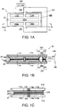
- Fig. 1A is a plan view illustrating a schematic configuration of a piezoelectric actuator 10.
- the piezoelectric actuator 10 includes piezoelectric elements 110a, 110b, 110c, 110d, and 110e, a substrate 200, and a projection member 20.
- the substrate 200 includes a vibrating portion 210 and a support portion 220 that supports the vibrating portion 210.
- the vibrating portion 210 has an approximately rectangular shape in which the piezoelectric elements 110a, 110b, 110c, 110d, and 110e are arranged.
- the piezoelectric element 110e is configured to have an approximately rectangular shape and is configured to extend in the longitudinal direction of the vibrating portion 210 at the widthwise center of the vibrating portion 210.
- the piezoelectric elements 110a, 110b, 110c, and 110d are configured to be positioned at four corners of the vibrating portion 210.
- the support portion 220 is configured to surround approximately half of the vibrating portion 210, and end portions of the support portion 220 are connected to the vibrating portion 210 at the center of the long edge of the vibrating portion 210.
- the end portions of the support portion 220 connected to the vibrating portion 210 will be referred to as "first connected portion 222", and "second connected portion 223”, and the part of the support portion 220 other than the first connected portion 222 and the second connected portion 223 will be referred to as "fixed portion 221".
- An interval 205 is configured between the vibrating portion 210 and the support portion 220.
- the interval 205 is configured to have a size in which the vibrating portion 210, even if vibrated, does not contact the fixed portion 221 of the support portion 220.
- the projection member 20 is arranged on a short edge on the side of the vibrating portion 210 not surrounded by the support portion 220. That is, a region that has a protruding shape is arranged at the tip end of the vibrating portion 210.
- the projection member 20 is preferably configured of a durable material such as ceramic (for example, Al 2 O 3 ).
- Fig. 1B is a sectional view of the piezoelectric actuator 10 taken along 1B-1B in Fig. 1A .
- the piezoelectric actuator 10 includes two piezoelectric actuator units 100.
- Each of the two piezoelectric actuator units 100 includes the substrate 200 and the five piezoelectric elements 110a to 110e arranged on the substrate 200.
- Fig. 1B illustrates two piezoelectric elements 110c and 110d and does not illustrate the other three piezoelectric elements 110a, 110b, and 110e.
- the piezoelectric elements 110a to 110e are arranged on each of the facing surfaces of two substrates 200 in a region (the region of the vibrating portion 210) where the two substrates 200 overlie each other in a plan view ( Fig. 1A ).
- Two piezoelectric elements that are designated by the same reference sign, for example, two piezoelectric elements 110a, are positioned to be seen in an overlying manner in the plan view of the two substrates 200. The same applies to the other piezoelectric elements 110b to 110e.
- the two piezoelectric actuator units 100 are arranged in such a manner that the piezoelectric elements 110a to 110e are sandwiched between the two substrates 200 with the substrates 200 positioned outside.
- the piezoelectric elements 110a to 110e are covered with a protective layer 260.
- the "protective layer 260" will be referred to as "cladding portion 260" as well.
- the cladding portions 260 of the two piezoelectric actuator units 100 are bonded by a bond layer 270, and thereby the piezoelectric actuator 10 is configured.
- the projection member 20 may have a spherical shape or an ellipsoidal shape and be provided on each substrate 200.
- the piezoelectric actuator 10 as illustrated in Fig. 1B includes, on the support portion 220, a piezoelectric element structure 111 that has the same layer structure as the piezoelectric elements 110a to 110e.
- Two support portions 220 are arranged at an interval in a case where the piezoelectric actuator 10 does not include the piezoelectric element structure 111 on the support portion 220 of the substrate 200.
- the piezoelectric elements 110a to 110e are arranged between the two substrates 200 in the vibrating portion 210.
- the vibrating portion 210 and the support portion 220 have different thicknesses in a case where the piezoelectric element structure 111 is not included on the support portion 220.
- the piezoelectric actuator units 100 are not in contact in the support portion 220, and the structure may be unstable.
- the piezoelectric element structure 111 is included on the support portion 220, the thicknesses of the vibrating portion 210 and the support portion 220 approximately match, and the piezoelectric actuator units 100 are in contact in the support portion 220.
- the support portion 220 may be vibrated when the piezoelectric element structure 111 is expanded and contracted by a voltage applied thereto.
- the piezoelectric element structure 111 is preferably configured not to be expanded and contracted even if a voltage is applied thereto or in such a manner that a voltage is not applied to a piezoelectric body thereof.
- two electrodes between which the piezoelectric body of the piezoelectric element structure 111 is sandwiched may be grounded or short-circuited.
- Fig. 1C is a side view of the piezoelectric actuator 10.
- Fig. 1C illustrates the side view in the vibrating portion 210 and does not illustrate the side view in the support portion 220 ( Figs. 1A and 1B ).
- the cladding portion 260 covers the side surfaces of the piezoelectric elements 110a to 110e as well.
- Fig. 2A is a top view of one piezoelectric actuator unit 100.
- Fig. 2A illustrates the vibrating portion 210 and does not illustrate the support portion 220 except for parts corresponding to the first connected portion 222 and the second connected portion 223.
- Each of the piezoelectric elements 110a to 110e of the piezoelectric actuator unit 100 is covered with the cladding portion 260.
- the cladding portion 260 does not exist in regions that are in contact with the first connected portion 222 and the second connected portion 223.
- the cladding portion 260 is said to cover at least a part of the surrounding area of the piezoelectric elements 110a to 110e.
- the cladding portion 260 may entirely cover the surrounding area of the piezoelectric elements 110a to 110e.
- Fig. 2B is a sectional view of one piezoelectric actuator unit 100 in the second connected portion 223.
- the vibrating portion 210 is illustrated by a broken line in Fig. 2B .
- the piezoelectric elements 110a to 110e and the cladding portion 260 on the vibrating portion 210 are not illustrated.
- Wirings 252 and 253 are seen on the second connected portion 223.
- the cladding portion 260 is not arranged on the second connected portion 223.
- the cladding portion 260 is not arranged on the first connected portion 222 though not illustrated.
- the cladding portion 260 is not required to cover the entire piezoelectric elements 110a to 110e and may not cover a part of the surrounding area thereof (for example, parts corresponding to the wirings 252 and 253).
- the cladding portion 260 may entirely cover the surrounding area of the piezoelectric elements 110a to 110e.
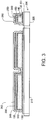
- Fig. 3 is a descriptive diagram illustrating a section of the piezoelectric actuator unit 100 in detail.
- the piezoelectric actuator unit 100 is such that members including an insulating layer 201, a first electrode 130, a piezoelectric body 140, a second electrode 150, an insulating layer 240, a wiring layer 250, and the protective layer 260 (cladding portion 260) are arranged in this order on the substrate 200.
- the insulating layer 201 insulates the substrate 200 from other electrodes (the first electrode 130, the second electrode 150, and the wiring layer 250).
- the first electrode 130, the piezoelectric body 140, and the second electrode 150 constitute the piezoelectric elements 110a to 110e.
- the insulating layer 240 covers and insulates the piezoelectric elements 110a to 110e.
- the insulating layer 240 includes a contact hole that is used to cause the first electrodes 130 and the second electrodes 150 of the piezoelectric elements 110a to 110e to be in contact with the wiring layer 250.
- the wiring layer 250 constitutes a wiring that is used to conduct electricity to the first electrode 130 and the second electrode 150.
- the protective layer 260 (cladding portion 260) protects the piezoelectric elements 110a to 110e as described above.
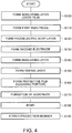
- Fig. 4 is a flowchart illustrating manufacturing processes for the piezoelectric actuator.
- Fig. 5 is a descriptive diagram illustrating manufacturing processes for the piezoelectric actuator unit.
- the insulating layer 201 is formed on the substrate 200.
- An Si wafer for example, can be used as the substrate 200.
- the piezoelectric actuator unit 100 maybe formed in multiple quantities on one Si wafer.
- An SiO 2 layer for example, that is formed by thermal oxidation of the surface of the substrate 200 can be used as the insulating layer 201.
- the insulating layer 201 is not illustrated in Fig. 1B and the like.
- An organic material such as alumina (Al 2 O 3 ), acryl, and polyimide can be used as the insulating layer 201.
- the process of forming the insulating layer 201 may be omitted in a case where the substrate 200 is an insulating body.
- the first electrode 130 is formed and is patterned. Any material having high conductivity, such as aluminum (Al), nickel (Ni), gold (Au), platinum (Pt), iridium (Ir), and copper (Cu), may be used as the material of the first electrode 130.
- the first electrode 130 can be formed by, for example, sputtering and can be patterned by, for example, etching.
- the piezoelectric body 140 is formed on the first electrode 130 and is patterned. Any material exhibiting a piezoelectric effect, such as ceramic that adopts the ABO 3 perovskite structure, may be used as the material of the piezoelectric body 140.
- any material exhibiting a piezoelectric effect such as ceramic that adopts the ABO 3 perovskite structure, may be used as the material of the piezoelectric body 140.
- PZT lead zirconate titanate
- barium titanate, lead titanate, potassium niobate, lithium niobate, lithium tantalate, sodium tungstate, zinc oxide, barium strontium titanate (BST), strontium bismuth tantalate (SBT), lead metaniobate, lead zinc niobate, and lead scandium niobate may be used as the ceramic that adopts the ABO 3 perovskite structure.
- Materials other than ceramic that exhibit a piezoelectric effect such as polyvinylidene flu
- the piezoelectric body 140 may be formed by using, for example, the sol-gel method. That is, a sol-gel solution as a piezoelectric body material is dripped onto the substrate 200 (first electrode 130), and the substrate 200 is rotated at a high speed to form a thin film of the sol-gel solution on the first electrode 130. Then, calcination is performed at a temperature of 200°C to 300°C to form a first layer of the piezoelectric body material on the first electrode 130. Then, the cycle of sol-gel solution dripping, high-speed rotation, and calcination is repeated multiple times to form a piezoelectric body layer to a desired thickness on the first electrode 130.
- the sol-gel method That is, a sol-gel solution as a piezoelectric body material is dripped onto the substrate 200 (first electrode 130), and the substrate 200 is rotated at a high speed to form a thin film of the sol-gel solution on the first electrode 130. Then, calcination is performed at a temperature
- the thickness of one layer of the piezoelectric body formed in one cycle is a thickness of approximately 50 nm to 150 nm.
- sintering is performed at a temperature of 600°C to 1,000°C to form the piezoelectric body 140. If the thickness of the piezoelectric body 140 after sintering is greater than or equal to 50 nm (0.05 ⁇ m) and less than or equal to 20 ⁇ m, the piezoelectric actuator 10 can be implemented to have a small size. If the thickness of the piezoelectric body 140 is greater than or equal to 0 .
- sufficiently large force can be generated in response to expansion and contraction of the piezoelectric body 140. If the thickness of the piezoelectric body 140 is less than or equal to 20 ⁇ m, sufficiently large force can be generated even if the voltage applied to the piezoelectric body 140 is less than or equal to 600 V. As a result, a drive circuit (not illustrated) that is used to drive the piezoelectric actuator 10 can be configured of inexpensive elements. The thickness of the piezoelectric body may be greater than or equal to 400 nm. In this case, large force can be generated by the piezoelectric elements. The temperatures and the times of calcination and sintering are examples and are appropriately chosen according to the piezoelectric body material.
- Performing sintering after a thin film of the piezoelectric body material is formed with the use of the sol-gel method has advantages over a related art sintering method that mixes powder of raw materials and performs sintering, in that (a) the thin film is easily formed, (b) crystallization is easily performed with aligned lattice directions, and (c) the breakdown voltage of the piezoelectric body can be improved.
- Patterning of the piezoelectric body 140 in the first embodiment is performed in Step S120 by ion milling that uses an argon ion beam. Instead of patterning using ion milling, patterning may be performed by any other patterning methods (for example, dry etching that uses chlorine-based gas).
- Step S130 the second electrode 150 is formed on the piezoelectric body 140 and is patterned. Forming and patterning of the second electrode 150 can be performed by etching in the same manner as the first electrode 130.
- Step S140 the insulating layer 240 is formed on the second electrode 150 and is patterned to form a contact hole.
- the wiring layer 250 is formed on the insulating layer 240 by using copper or brass, and the wiring layer 250 is patterned to form wirings.
- Fig. 6 is a descriptive diagram illustrating a wiring pattern provided by the wiring layer 250.
- the wiring layer 250 includes four wirings 251, 252, 253, and 254.
- the wirings 251 to 254 are formed to reach the vibrating portion 210 through the connected portion 222 or 223 from the fixed portion 221. That is, the wirings 251 to 254 are arranged to connect the vibrating portion 210 and the support portion 220.
- the first wiring 251 is connected to the second electrodes 150 of the piezoelectric elements 110a and 110d ( Figs. 1A to 1C ) in the vibrating portion 210.
- the second wiring 252 is connected to the second electrodes 150 of the piezoelectric elements 110b and 110c in the vibrating portion 210.
- the third wiring 253 is connected to the second electrode 150 of the piezoelectric element 110e in the vibrating portion 210.
- the fourth wiring 254 is connected to the first electrodes 130 of the piezoelectric elements 110a, 110b, 110c, 110d, and 110e in the vibrating portion 210.
- the wirings 251 to 254 are connected to a circuit substrate in the support portion 220.
- the wirings 251 to 254 are not connected to the piezoelectric element structure 111 of the fixed portion 221.
- the protective layer 260 (cladding portion 260) is formed.
- the cladding portion 260 is formed of silicone resin such as junction coating resin (JCR). Instead of JCR, resin materials such as epoxy and polyimide may be used to form the cladding portion 260.
- JCR junction coating resin
- Step S170 etching is performed to form the interval 205 between the vibrating portion 210 and the support portion 220 and to form a recess portion 216 that is used to attach the projection member 20, along with forming the shapes of the individual substrates 200.
- Fig. 7 is a descriptive diagram illustrating processes of manufacturing the piezoelectric actuator 10 using the two piezoelectric actuator units 100.
- Step S180 the two piezoelectric actuator units 100 are arranged in such a manner that members designated by the same reference sign are in plane symmetry with the substrates 200 positioned outside and the piezoelectric elements 110a to 110e directed inward.
- the cladding portions 260 of the two piezoelectric actuator units 100 are bonded by using the bond layer 270.
- the piezoelectric elements 110a to 110e are covered with the cladding portion 260 and are sandwiched between the two substrates 200 and thus are unlikely to experience external damage caused by dust.
- Step S190 the projection member 20 is bonded to the recess portion 216 by adhesive.
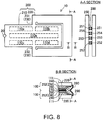
- Fig. 8 is a descriptive diagram of a connected portion between the piezoelectric actuator 10 and a circuit substrate (not illustrated).
- the piezoelectric actuator 10 is connected to an external circuit substrate in the support portion 220.
- An insulating layer (the insulating layer 201 in Fig. 3 ; not illustrated in Fig. 8 ) is formed on the support portion 220 (substrate 200).
- the piezoelectric element structure 111, the insulating layer 240, the wiring 252 (the second wiring 252 of the wirings 251 to 254 of the wiring layer 250 is seen in the section taken along B-B in Fig. 8 ) and the protective layer 260 (cladding portion 260) are formed in order on the insulating layer in the support portion 220.
- the second wiring 252 is formed from the top of the piezoelectric element structure 111 to a position in which the piezoelectric element structure 111 is not formed in the support portion 220.
- An electroless nickel plating layer 280 is formed between two second wirings 252.
- a gold plating layer 290 is formed on the electroless nickel plating layer 280.
- Fig. 9 is a descriptive diagram illustrating processes of connecting the piezoelectric actuator and the circuit substrate. While the second wiring 252 will be illustratively described, the same applies to the other wirings 251, 253, and 254.
- the electroless nickel plating layer 280 is formed on the second wiring 252.
- an end portion of the piezoelectric actuator 10 is immersed in a catalyst solution that includes palladium ions. Since the second wiring 252 is formed of copper or brass, a part of copper is replaced by palladium, and palladium metal is adsorbed to the second wiring 252.
- the electroless nickel-phosphorus plating liquid includes nickel ions (Ni 2+ ) and hypophosphite ions (H 2 PO 2 - ) .
- Nickel ions (Ni 2+ ) and hypophosphite ions (H 2 PO 2 - ) cause an oxidation-reduction reaction described below with palladium as a catalyst, and reduced nickel is precipitated on the second wiring 252. Since nickel is precipitated along the second wiring 252, the nickel has a shape including a projection portion 285 that protrudes to the outer edge side from the substrate 200 along the substrate 200 (support portion 220).
- the nickel may include phosphorus when precipitated.
- Step S210 the gold plating layer 290 is formed on the electroless nickel plating layer 280.
- Step S220 the piezoelectric actuator 10 is bonded to a circuit substrate 300.
- the circuit substrate 300 has a structure in which wirings are formed on a flexible substrate.
- the projection portion 285 is intruded into the circuit substrate 300 by pressing the projection portion 285 including the gold plating layer 290 to the circuit substrate 300, and thereby the piezoelectric actuator 10 and the circuit substrate 300 are bonded and electrically connected.
- Fig. 10 is a descriptive diagram illustrating an equivalent circuit of the piezoelectric actuator 10. While the piezoelectric actuator 10 includes two piezoelectric actuator units 100, Fig. 10 illustrates only one piezoelectric actuator unit 100. As understood from Fig. 10 , the first electrodes 130 of the five piezoelectric elements 110a to 110e are connected to the wiring 254 and are connected to the circuit substrate 300. The second electrodes 150 of the piezoelectric elements 110a and 110d are connected to the wiring 251 and are connected to the circuit substrate 300. The second electrodes 150 of the piezoelectric elements 110b and 110c are connected to the wiring 252 and are connected to the circuit substrate 300.
- the second electrode 150 of the piezoelectric element 110e is connected to the wiring 253 and is connected to the circuit substrate 300. That is, the piezoelectric elements 110a to 110e are divided into three groups. A first group includes two piezoelectric elements 110a and 110d. A second group includes two piezoelectric elements 110b and 110c. A third group includes only one piezoelectric element 110e. The piezoelectric elements 110a and 110d of the first group are connected in parallel with each other and are connected to the circuit substrate 300. The piezoelectric elements 110b and 110c of the second group are connected in parallel with each other and are connected to the circuit substrate 300. Large voltages can be applied to each of the piezoelectric elements 110a to 110d when parallel connection is made.
- the piezoelectric element 110e of the third group is connected to the circuit substrate 300 alone.
- the piezoelectric elements 110a and 110d of the first group may be connected in series. In this case, the directions of polarization of the piezoelectric elements 110a and 110d when voltages are applied are preferably the same.
- the piezoelectric elements 110b and 110c of the second group may be connected in series as well. Capacitance can be decreased when serial connection is made.
- a periodically changing alternating current voltage or an undulating voltage from the circuit substrate 300 between the first electrode 130 and the second electrode 150 of a predetermined piezoelectric element for example, the piezoelectric elements 110a and 110d of the first group, of the five piezoelectric elements 110a to 110e causes the piezoelectric actuator 10 to be subjected to ultrasonic vibration and allows a rotor (a driven body; a driven member) that is in contact with the proj ection member 20 to be rotated in a predetermined direction of rotation.
- the "undulating voltage” means a voltage obtained by adding a DC offset to an alternating current voltage.
- the voltage (electric field) of the undulating voltage is unidirectional from one electrode to another electrode.
- the direction of a current is preferably a direction from the second electrode 150 to the first electrode 130 rather than a direction from the first electrode 130 to the second electrode 150.
- Applying an alternating current voltage or an undulating voltage between the first electrode 130 and the second electrode 150 of the piezoelectric elements 110b and 110c of the second group allows the rotor which is in contact with the projection member 20 to be rotated in the opposite direction. That is, the piezoelectric actuator 10 functions as a piezoelectric motor.
- Fig. 11 is a descriptive diagram illustrating an example of operation of the piezoelectric actuator 10.
- the support portion 220 is not illustrated for convenience of illustration.
- the projection member 20 of the piezoelectric actuator 10 is in contact with the circumference of a rotor 50 that is a driven member.
- An alternating current voltage or an undulating voltage is applied to the two piezoelectric elements 110a and 110d of the first group in the example illustrated in Fig. 11 , and the piezoelectric elements 110a and 110d are expanded and contracted in the direction of an arrow x in Fig. 11 .
- the vibrating portion 210 of the piezoelectric actuator 10 is bent in the plane of the vibrating portion 210 and is deformed into a meander shape (S shape), and the tip end of the projection member 20 reciprocates in the direction of an arrow y or moves elliptically.
- the rotor 50 rotates in a predetermined direction z (a clockwise direction in Fig. 11 ) around a center 51 thereof.
- the rotor 50 rotates in the opposite direction in a case where the circuit substrate 300 applies an alternating current voltage or an undulating voltage to the two piezoelectric elements 110b and 110c ( Fig. 10 ) of the second group.
- the piezoelectric actuator 10 If an alternating current voltage or an undulating voltage is applied to the piezoelectric element 110e at the center, the piezoelectric actuator 10 is expanded and contracted in the longitudinal direction. Thus, larger force may be exerted on the rotor 50 from the projection member 20.
- Such operation of the piezoelectric actuator 10 is disclosed in JP-A-2004-320979 (or corresponding U.S. Patent No. 7224102 ), the content of disclosure of which is incorporated herein by reference.
- the piezoelectric actuator 10 includes the piezoelectric elements 110a to 110e that are arranged between two substrates 200, and the cladding portion 260 that covers at least a part of the surrounding area of the piezoelectric elements 110a to 110e.
- the piezoelectric elements 110a to 110e are unlikely to experience external damage since being protected by the two substrates 200 and the cladding portion 260.
- the piezoelectric actuator 10 includes two substrates 200 that are arranged to at least partially overlie each other in a plan view, the piezoelectric elements 110a to 110e that are arranged on each of the facing surfaces of the two substrates 200 in the region where the two substrates 200 overlie each other in a plan view (the region of the vibrating portion 210), and the cladding portion 260 that covers the piezoelectric elements 110a to 110e in each piezoelectric actuator unit 100.
- the piezoelectric elements 110a to 110e are covered with the cladding portion 260 and are arranged on each of the facing surfaces of two substrates 200 that are arranged to at least partially overlie each other.
- the piezoelectric elements 110a to 110e are protected by the two substrates 200 as well and are unlikely to experience external damage.
- the cladding portions 260 that cover the piezoelectric elements 110a to 110e of each piezoelectric actuator unit 100 are bonded to each other by the bond layer 270.
- the two cladding portions 260 are unlikely to be separated, and the piezoelectric elements 110a to 110e are easily protected.
- the substrate 200 includes the vibrating portion 210 and the support portion 220, and the piezoelectric elements 110a to 110e are provided in the vibrating portion 210.
- vibration of the support portion 220 can be reduced, and the strength of the substrate 200 can be increased.
- the cladding portion 260 may cover the entire piezoelectric elements 110a to 110e. If the cladding portion 260 covers the entire piezoelectric elements 110a to 110e, the piezoelectric elements 110a to 110e are more easily protected.
- the above embodiment may adopt a configuration in which the cladding portion 260 covers at least a part of the surrounding area of the support portion 220. If the cladding portion 260 covers at least a part of the surrounding area of the support portion 220, the support portion 220 can be protected.
- Fig. 12 is a descriptive diagram illustrating a piezoelectric actuator 11 of a second embodiment. While the piezoelectric actuator 10 of the first embodiment includes two piezoelectric actuator units 100, the piezoelectric actuator 11 of the second embodiment includes only one piezoelectric actuator unit 100 and, instead of the second piezoelectric actuator unit 100 of the first embodiment, includes the substrate 200 on which piezoelectric elements are not arranged. That is, the piezoelectric elements 110a to 110e of the first piezoelectric actuator unit 100 are sandwiched between the substrate 200 of the first piezoelectric actuator unit 100 and the substrate 200 on which piezoelectric elements are not arranged.
- the piezoelectric actuator 11 of the second embodiment includes two substrates 200, the piezoelectric elements 110a to 110e that are arranged between the two substrates 200, and the cladding portion 260 that covers at least a part of the surrounding area of the piezoelectric elements. According to the piezoelectric actuator 11 of the second embodiment, the effect that the piezoelectric elements 110a to 110e are protected by the two substrates 200 and the cladding portion 260 is high. Thus, the piezoelectric elements 110a to 110e are unlikely to experience external damage in the same manner as the piezoelectric actuator 10 of the first embodiment.
- Fig. 13 is a descriptive diagram illustrating a stacked actuator 12 of a third embodiment.
- the piezoelectric actuator 10 is described in the first embodiment.
- the piezoelectric actuator 10 may be used in multiple quantities and be stacked in the direction normal to the surface of the substrate 200 to configure the stacked actuator 12.
- the piezoelectric actuator 11 of the second embodiment as well may be used in multiple quantities and be stacked in the direction normal to the surface of the substrate 200.
- the piezoelectric actuator 10 described above can exert large force on the driven member using resonance and is applicable to various apparatuses.
- the piezoelectric actuator 10 can be used as a drive device in various apparatuses such as a robot (includes an electronic component transport apparatus (IC handler) as well), a pump for medication administration, a calendar advancing apparatus for a timepiece, and a printing apparatus (for example, a paper feeding mechanism; the piezoelectric actuator 10 is not applicable to a head since a piezoelectric actuator used in the head does not cause a vibrating plate to resonate.).
- a robot includes an electronic component transport apparatus (IC handler) as well
- a pump for medication administration for medication administration
- calendar advancing apparatus for a timepiece for example, a timepiece
- a printing apparatus for example, a paper feeding mechanism
- the piezoelectric actuator 10 is not applicable to a head since a piezoelectric actuator used in the head does not cause a vibrating plate to resonate.
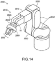
- Fig. 14 is a descriptive diagram illustrating one example of a robot 2050 that uses the piezoelectric actuator 10 described above.
- the robot 2050 includes an arm 2010 (referred to as "arm unit” as well) that includes multiple link units 2012 (referred to as “link members” as well) and multiple joint units 2020 that provide pivotable or bendable connection between the link units 2012.
- the piezoelectric actuator 10 described above is incorporated in each joint unit 2020.
- the joint units 2020 may be pivoted or bent any angle by using the piezoelectric actuator 10.
- a hand 2000 is connected to the tip end of the arm 2010.
- the hand 2000 includes a pair of clasping units 2003.
- the piezoelectric actuator 10 is incorporated in the hand 2000 as well.
- An object may be clasped by opening and closing the clasping units 2003 using the piezoelectric actuator 10.
- the piezoelectric actuator 10 is provided between the hand 2000 and the arm 2010 as well.
- the hand 2000 may be rotated with respect to the arm 2010 by using the piezoelectric actuator 10.
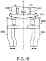
- Fig. 15 is a descriptive diagram of a wrist part of the robot 2050 illustrated in Fig. 14 .
- the joint units 2020 of the wrist pinch a wrist pivoting unit 2022, and the link unit 2012 of the wrist is attached to the wrist pivoting unit 2022 in a pivotable manner around a central axis O of the wrist pivoting unit 2022.
- the wrist pivoting unit 2022 includes the piezoelectric actuator 10, and the piezoelectric actuator 10 pivots the link portion 2012 of the wrist and the hand 2000 around the central axis O.
- Multiple clasping units 2003 are erected on the hand 2000.
- a base portion of the clasping unit 2003 is movable in the hand 2000.
- the piezoelectric actuator 10 is mounted in a root part of the clasping unit 2003.
- the clasping unit 2003 can be moved by operating the piezoelectric actuator 10 to clasp a target object.
- the robot is not limited to a single-arm robot.
- the piezoelectric actuator 10 is also applicable to a multi-arm robot that includes two or more arms. Power lines that supply power to various devices such as a force sensor and a gyrosensor, signal lines that transmit signals, and the like are included in the joint units 2020 of the wrist and in the hand 2000 in addition to the piezoelectric actuator 10, and a significantly large number of wirings are required. Therefore, it is significantly difficult to arrange wirings in the joint units 2020 and the hand 2000.
- a drive current of the piezoelectric actuator 10 of the embodiment described above can be rendered smaller than that of a typical electric motor or a piezoelectric drive device of the related art.
- wirings may be arranged in a small space such as the joint units 2020 (particularly, the joint units at the tip end of the arm 2010) and the hand 2000.
- the hand 2000 may be configured as not only a component of the robot 2050 but also a single product.
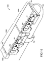
- Fig. 16 is a descriptive diagram illustrating a finger assist apparatus 1000 that uses the piezoelectric actuator 10 described above.
- the finger assist apparatus 1000 includes a first finger assist unit 1001, a second finger assist unit 1002, and a base member 1003 and is mounted on a finger 700.
- the first finger assist unit 1001 includes the piezoelectric actuator 10, a speed reducer 501, and a finger support portion 701.
- the second finger assist unit 1002 includes the piezoelectric actuator 10, a speed reducer 502, a finger support portion 702, and a band 703.
- the first finger assist unit 1001 has approximately the same configuration as the second finger assist unit 1002 except for the band 703.
- the band 703 fixes the second finger assist unit 1002 from the belly side of the finger 700.
- the band 703 is provided in the first finger assist unit 1001 as well, though not illustrated in Fig. 16 .
- the finger assist apparatus 1000 assists bending and stretching of the finger 700 using the piezoelectric actuator 10. While the finger assist apparatus 1000 is described as assisting bending and stretching of the finger 700 in the present embodiment, a hand of a robot may be used instead of the finger 700, and the finger assist apparatus 1000 may be integrated with the hand. In this case, the hand is driven to be bent and stretched by the piezoelectric actuator 10.
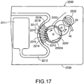
- Fig. 17 is a descriptive diagram illustrating one example of a liquid transport pump 2200 that uses the piezoelectric actuator 10 described above.
- a reservoir 2211, a tube 2212, the piezoelectric actuator 10, a rotor 2222, a speed reducing transmission mechanism 2223, a cam 2202, and multiple fingers 2213, 2214, 2215, 2216, 2217, 2218, and 2219 are provided in a case 2230 of the liquid transport pump 2200.
- the reservoir 2211 is an accommodation unit that is used to accommodate transport target liquid.
- the tube 2212 is a tube that is used to transport liquid carried out of the reservoir 2211.
- the projection member 20 of the piezoelectric actuator 10 is provided in a pressed state to a side surface of the rotor 2222, and the piezoelectric actuator 10 rotationally drives the rotor 2222.
- the force of rotation of the rotor 2222 is transmitted to the cam 2202 through the speed reducing transmission mechanism 2223.
- the fingers 2213 to 2219 are members that are used to occlude the tube 2212.
- a protrusion portion 2202A of the cam 2202 presses the fingers 2213 to 2219 in order in an outwardly radial direction.
- the fingers 2213 to 2219 occlude the tube 2212 in order from the upstream side (reservoir 2211 side) in the direction of transport.
- liquid in the tube 2212 is transported in order to the downstream side.
- the arrangement of each member is not limited to the illustration. A configuration that does not include members such as fingers and occludes the tube 2212 with a ball and the like provided in the rotor 2222 may be used as well.
- the liquid transport pump 2200 described above can be used in, for example, a medication administering apparatus that administers liquid medication such as insulin to a human body. Since the drive current is rendered smaller than that of the piezoelectric drive device of the related art by using the piezoelectric actuator 10 of the embodiments described above, power consumption of the medication administering apparatus can be reduced. Therefore, the liquid transport pump 2200 is particularly effective in a case where the medication administering apparatus is battery driven.
Landscapes
- Engineering & Computer Science (AREA)
- Mechanical Engineering (AREA)
- Robotics (AREA)
- Manufacturing & Machinery (AREA)
- General Engineering & Computer Science (AREA)
- Chemical & Material Sciences (AREA)
- Ceramic Engineering (AREA)
- General Electrical Machinery Utilizing Piezoelectricity, Electrostriction Or Magnetostriction (AREA)
- Reciprocating Pumps (AREA)
Abstract

Description
- The present invention relates to a piezoelectric actuator and various apparatuses that use the piezoelectric actuator.
- Known is a piezoelectric actuator in which piezoelectric bodies are bonded to both surfaces of a shim material and the surrounding area of the piezoelectric bodies is covered with resin (for example,
JP-A-2006-80318 - The piezoelectric actuator of
JP-A-2006-80318 - An advantage of some aspects of the invention is to solve at least a part of the problems described above, and the invention can be implemented as the following aspects.
- (1) According to an aspect of the invention, a piezoelectric actuator is provided. The piezoelectric actuator includes two substrates, a piezoelectric element that is arranged between the two substrates, and a cladding portion that covers at least a part of the piezoelectric element. According to this aspect, the piezoelectric element is unlikely to experience external damage since being protected by the two substrates and the cladding portion.
- (2) According to another aspect of the invention, a piezoelectric actuator is provided. The piezoelectric actuator includes two substrates that are arranged to at least partially overlie each other in a plan view, piezoelectric elements that are respectively arranged on facing surfaces of the two substrates in a region where the two substrates overlie each other in the plan view, and cladding portions that respectively cover at least parts of the two piezoelectric elements. According to this aspect, the piezoelectric elements are covered with the cladding portions and are respectively arranged on the facing surfaces of the two substrates that are arranged to at least partially overlie each other. Thus, the piezoelectric elements are protected by the two substrates as well and are unlikely to experience external damage.
- (3) In the aspect, it is preferable that a bond layer is arranged between the two cladding portions. According to this aspect, since the bond layer is arranged between the two cladding portions, the two cladding portions are unlikely to be separated, and the piezoelectric elements are easily protected.
- (4) In the aspect, it is preferable that the substrate includes a vibrating portion and a support portion that supports the vibrating portion and that the two piezoelectric elements are provided in the vibrating portion. According to this aspect, vibration of the support portion can be reduced, and the strength of the substrate can be increased.
- (5) In the aspect, it is preferable that the cladding portion entirely covers the piezoelectric element. According to this aspect, the piezoelectric element is easily protected since the cladding portion entirely covers the piezoelectric element.
- (6) In the aspect, it is preferable that the cladding portion covers at least a part of a surrounding area of the support portion. According to this aspect, the support portion is protected as well since the cladding portion covers at least a part of the surrounding area of the support portion.
- (7) In the aspect, it is preferable that a protruding region is included at a tip end of the vibrating portion. According to this aspect, vibration of the vibrating portion can be transmitted to other members by using the protruding region.
- (8) In the aspect, it is preferable that the piezoelectric actuator further includes a wiring layer that is arranged to connect the vibrating portion and the support portion, and a circuit substrate that is electrically connected to the wiring layer and is connected to the support portion. Vibration of the vibrating portion is unlikely to affect the circuit substrate since the circuit substrate is connected to the support portion.
- (9) According to still another aspect of the invention, a stacked actuator is provided. The stacked actuator includes a plurality of the piezoelectric actuators in stack formation. According to this aspect, driving power of the stacked actuator can be increased.
- The invention can be implemented in various aspects and, for example, can be implemented in various aspects in addition to the piezoelectric actuator and the stacked actuator, such as a piezoelectric motor that includes the piezoelectric actuator or the stacked actuator, and a robot, a hand, and a liquid transport pump that include the piezoelectric motor.
- The invention will be described with reference to the accompanying drawings, wherein like numbers reference like elements.
-
Fig. 1A is a plan view illustrating a schematic configuration of a piezoelectric actuator. -
Fig. 1B is a sectional view of the piezoelectric actuator. -
Fig. 1C is a side view of the piezoelectric actuator. -
Fig. 2A is a top view of a piezoelectric actuator unit. -
Fig. 2B is a sectional view of the piezoelectric actuator unit in a second connected portion. -
Fig. 3 is a descriptive diagram illustrating the piezoelectric actuator unit in an enlarged manner. -
Fig. 4 is a flowchart illustrating manufacturing processes for the piezoelectric actuator. -
Fig. 5 is a descriptive diagram illustrating manufacturing processes for the piezoelectric actuator unit. -
Fig. 6 is a descriptive diagram illustrating a wiring pattern provided by a wiring electrode. -
Fig. 7 is a descriptive diagram illustrating processes of manufacturing the piezoelectric actuator using two piezoelectric actuator units. -
Fig. 8 is a descriptive diagram of a connected portion between the piezoelectric actuator and a circuit substrate. -
Fig. 9 is a descriptive diagram illustrating processes of connecting the piezoelectric actuator and a substrate. -
Fig. 10 is a descriptive diagram illustrating an equivalent circuit of the piezoelectric actuator. -
Fig. 11 is a descriptive diagram illustrating an example of operation of the piezoelectric actuator. -
Fig. 12 is a descriptive diagram illustrating a piezoelectric actuator of a second embodiment. -
Fig. 13 is a descriptive diagram illustrating a stacked actuator of a third embodiment. -
Fig. 14 is a descriptive diagram illustrating one example of a robot that uses a piezoelectric actuator (piezoelectric motor). -
Fig. 15 is a descriptive diagram illustrating a hand that uses a piezoelectric actuator (piezoelectric motor). -
Fig. 16 is a descriptive diagram illustrating a finger assist apparatus that uses a piezoelectric actuator. -
Fig. 17 is a descriptive diagram illustrating one example of a liquid transport pump that uses a piezoelectric actuator (piezoelectric motor). -
Fig. 1A is a plan view illustrating a schematic configuration of apiezoelectric actuator 10. Thepiezoelectric actuator 10 includespiezoelectric elements substrate 200, and aprojection member 20. Thesubstrate 200 includes a vibratingportion 210 and asupport portion 220 that supports the vibratingportion 210. The vibratingportion 210 has an approximately rectangular shape in which thepiezoelectric elements piezoelectric element 110e is configured to have an approximately rectangular shape and is configured to extend in the longitudinal direction of the vibratingportion 210 at the widthwise center of the vibratingportion 210. Thepiezoelectric elements portion 210. Thesupport portion 220 is configured to surround approximately half of the vibratingportion 210, and end portions of thesupport portion 220 are connected to the vibratingportion 210 at the center of the long edge of the vibratingportion 210. The end portions of thesupport portion 220 connected to the vibratingportion 210 will be referred to as "first connectedportion 222", and "secondconnected portion 223", and the part of thesupport portion 220 other than the firstconnected portion 222 and the secondconnected portion 223 will be referred to as "fixedportion 221". Aninterval 205 is configured between the vibratingportion 210 and thesupport portion 220. When a voltage is applied to thepiezoelectric elements 110a to 110e, thepiezoelectric elements 110a to 110e are expanded and contracted, and the vibratingportion 210 is vibrated. Theinterval 205 is configured to have a size in which the vibratingportion 210, even if vibrated, does not contact the fixedportion 221 of thesupport portion 220. Theprojection member 20 is arranged on a short edge on the side of the vibratingportion 210 not surrounded by thesupport portion 220. That is, a region that has a protruding shape is arranged at the tip end of the vibratingportion 210. Theprojection member 20 is preferably configured of a durable material such as ceramic (for example, Al2O3). -
Fig. 1B is a sectional view of thepiezoelectric actuator 10 taken along 1B-1B inFig. 1A . Thepiezoelectric actuator 10 includes twopiezoelectric actuator units 100. Each of the twopiezoelectric actuator units 100 includes thesubstrate 200 and the fivepiezoelectric elements 110a to 110e arranged on thesubstrate 200.Fig. 1B illustrates twopiezoelectric elements piezoelectric elements piezoelectric elements 110a to 110e are arranged on each of the facing surfaces of twosubstrates 200 in a region (the region of the vibrating portion 210) where the twosubstrates 200 overlie each other in a plan view (Fig. 1A ). Two piezoelectric elements that are designated by the same reference sign, for example, twopiezoelectric elements 110a, are positioned to be seen in an overlying manner in the plan view of the twosubstrates 200. The same applies to the otherpiezoelectric elements 110b to 110e. The twopiezoelectric actuator units 100 are arranged in such a manner that thepiezoelectric elements 110a to 110e are sandwiched between the twosubstrates 200 with thesubstrates 200 positioned outside. Thepiezoelectric elements 110a to 110e are covered with aprotective layer 260. The "protective layer 260" will be referred to as "claddingportion 260" as well. Thecladding portions 260 of the twopiezoelectric actuator units 100 are bonded by abond layer 270, and thereby thepiezoelectric actuator 10 is configured. Theprojection member 20, though the shape of theprojection member 20 is not described along withFig. 1A , has an approximately cylindrical shape and straddles the twosubstrates 200. Theprojection member 20 may have a spherical shape or an ellipsoidal shape and be provided on eachsubstrate 200. - The
piezoelectric actuator 10 as illustrated inFig. 1B includes, on thesupport portion 220, apiezoelectric element structure 111 that has the same layer structure as thepiezoelectric elements 110a to 110e. Twosupport portions 220 are arranged at an interval in a case where thepiezoelectric actuator 10 does not include thepiezoelectric element structure 111 on thesupport portion 220 of thesubstrate 200. Thepiezoelectric elements 110a to 110e are arranged between the twosubstrates 200 in the vibratingportion 210. The vibratingportion 210 and thesupport portion 220 have different thicknesses in a case where thepiezoelectric element structure 111 is not included on thesupport portion 220. Thus, thepiezoelectric actuator units 100 are not in contact in thesupport portion 220, and the structure may be unstable. When thepiezoelectric element structure 111 is included on thesupport portion 220, the thicknesses of the vibratingportion 210 and thesupport portion 220 approximately match, and thepiezoelectric actuator units 100 are in contact in thesupport portion 220. Thus, the structure is likely to be stable. Thesupport portion 220 may be vibrated when thepiezoelectric element structure 111 is expanded and contracted by a voltage applied thereto. Thus, thepiezoelectric element structure 111 is preferably configured not to be expanded and contracted even if a voltage is applied thereto or in such a manner that a voltage is not applied to a piezoelectric body thereof. For example, two electrodes between which the piezoelectric body of thepiezoelectric element structure 111 is sandwiched may be grounded or short-circuited. -
Fig. 1C is a side view of thepiezoelectric actuator 10. For convenience of illustration,Fig. 1C illustrates the side view in the vibratingportion 210 and does not illustrate the side view in the support portion 220 (Figs. 1A and 1B ). As understood fromFig. 1C , thecladding portion 260 covers the side surfaces of thepiezoelectric elements 110a to 110e as well. -
Fig. 2A is a top view of onepiezoelectric actuator unit 100.Fig. 2A illustrates the vibratingportion 210 and does not illustrate thesupport portion 220 except for parts corresponding to the firstconnected portion 222 and the secondconnected portion 223. Each of thepiezoelectric elements 110a to 110e of thepiezoelectric actuator unit 100 is covered with thecladding portion 260. Thecladding portion 260 does not exist in regions that are in contact with the firstconnected portion 222 and the secondconnected portion 223. Thecladding portion 260 is said to cover at least a part of the surrounding area of thepiezoelectric elements 110a to 110e. Thecladding portion 260 may entirely cover the surrounding area of thepiezoelectric elements 110a to 110e. -
Fig. 2B is a sectional view of onepiezoelectric actuator unit 100 in the secondconnected portion 223. The vibratingportion 210 is illustrated by a broken line inFig. 2B . Thepiezoelectric elements 110a to 110e and thecladding portion 260 on the vibratingportion 210 are not illustrated.Wirings connected portion 223. However, thecladding portion 260 is not arranged on the secondconnected portion 223. Similarly, thecladding portion 260 is not arranged on the firstconnected portion 222 though not illustrated. Thecladding portion 260 is not required to cover the entirepiezoelectric elements 110a to 110e and may not cover a part of the surrounding area thereof (for example, parts corresponding to thewirings 252 and 253). Thecladding portion 260 may entirely cover the surrounding area of thepiezoelectric elements 110a to 110e. -
Fig. 3 is a descriptive diagram illustrating a section of thepiezoelectric actuator unit 100 in detail. Thepiezoelectric actuator unit 100 is such that members including an insulatinglayer 201, afirst electrode 130, apiezoelectric body 140, asecond electrode 150, an insulatinglayer 240, awiring layer 250, and the protective layer 260 (cladding portion 260) are arranged in this order on thesubstrate 200. The insulatinglayer 201 insulates thesubstrate 200 from other electrodes (thefirst electrode 130, thesecond electrode 150, and the wiring layer 250). Thefirst electrode 130, thepiezoelectric body 140, and thesecond electrode 150 constitute thepiezoelectric elements 110a to 110e. The insulatinglayer 240 covers and insulates thepiezoelectric elements 110a to 110e. The insulatinglayer 240 includes a contact hole that is used to cause thefirst electrodes 130 and thesecond electrodes 150 of thepiezoelectric elements 110a to 110e to be in contact with thewiring layer 250. Thewiring layer 250 constitutes a wiring that is used to conduct electricity to thefirst electrode 130 and thesecond electrode 150. The protective layer 260 (cladding portion 260) protects thepiezoelectric elements 110a to 110e as described above. -
Fig. 4 is a flowchart illustrating manufacturing processes for the piezoelectric actuator.Fig. 5 is a descriptive diagram illustrating manufacturing processes for the piezoelectric actuator unit. In Step S100, the insulatinglayer 201 is formed on thesubstrate 200. An Si wafer, for example, can be used as thesubstrate 200. Thepiezoelectric actuator unit 100 maybe formed in multiple quantities on one Si wafer. An SiO2 layer, for example, that is formed by thermal oxidation of the surface of thesubstrate 200 can be used as the insulatinglayer 201. The insulatinglayer 201 is not illustrated inFig. 1B and the like. An organic material such as alumina (Al2O3), acryl, and polyimide can be used as the insulatinglayer 201. The process of forming the insulatinglayer 201 may be omitted in a case where thesubstrate 200 is an insulating body. - In Step S110, the
first electrode 130 is formed and is patterned. Any material having high conductivity, such as aluminum (Al), nickel (Ni), gold (Au), platinum (Pt), iridium (Ir), and copper (Cu), may be used as the material of thefirst electrode 130. Thefirst electrode 130 can be formed by, for example, sputtering and can be patterned by, for example, etching. - In Step S120, the
piezoelectric body 140 is formed on thefirst electrode 130 and is patterned. Any material exhibiting a piezoelectric effect, such as ceramic that adopts the ABO3 perovskite structure, may be used as the material of thepiezoelectric body 140. For example, lead zirconate titanate (PZT), barium titanate, lead titanate, potassium niobate, lithium niobate, lithium tantalate, sodium tungstate, zinc oxide, barium strontium titanate (BST), strontium bismuth tantalate (SBT), lead metaniobate, lead zinc niobate, and lead scandium niobate may be used as the ceramic that adopts the ABO3 perovskite structure. Materials other than ceramic that exhibit a piezoelectric effect, such as polyvinylidene fluoride and quartz crystal, may be used as well. - The
piezoelectric body 140 may be formed by using, for example, the sol-gel method. That is, a sol-gel solution as a piezoelectric body material is dripped onto the substrate 200 (first electrode 130), and thesubstrate 200 is rotated at a high speed to form a thin film of the sol-gel solution on thefirst electrode 130. Then, calcination is performed at a temperature of 200°C to 300°C to form a first layer of the piezoelectric body material on thefirst electrode 130. Then, the cycle of sol-gel solution dripping, high-speed rotation, and calcination is repeated multiple times to form a piezoelectric body layer to a desired thickness on thefirst electrode 130. The thickness of one layer of the piezoelectric body formed in one cycle, though depending on the viscosity of the sol-gel solution and the speed of rotation of thesubstrate 200, is a thickness of approximately 50 nm to 150 nm. After the piezoelectric body layer is formed to a desired thickness, sintering is performed at a temperature of 600°C to 1,000°C to form thepiezoelectric body 140. If the thickness of thepiezoelectric body 140 after sintering is greater than or equal to 50 nm (0.05 µm) and less than or equal to 20 µm, thepiezoelectric actuator 10 can be implemented to have a small size. If the thickness of thepiezoelectric body 140 is greater than or equal to 0 . 05 µm, sufficiently large force can be generated in response to expansion and contraction of thepiezoelectric body 140. If the thickness of thepiezoelectric body 140 is less than or equal to 20 µm, sufficiently large force can be generated even if the voltage applied to thepiezoelectric body 140 is less than or equal to 600 V. As a result, a drive circuit (not illustrated) that is used to drive thepiezoelectric actuator 10 can be configured of inexpensive elements. The thickness of the piezoelectric body may be greater than or equal to 400 nm. In this case, large force can be generated by the piezoelectric elements. The temperatures and the times of calcination and sintering are examples and are appropriately chosen according to the piezoelectric body material. - Performing sintering after a thin film of the piezoelectric body material is formed with the use of the sol-gel method has advantages over a related art sintering method that mixes powder of raw materials and performs sintering, in that (a) the thin film is easily formed, (b) crystallization is easily performed with aligned lattice directions, and (c) the breakdown voltage of the piezoelectric body can be improved.
- Patterning of the
piezoelectric body 140 in the first embodiment is performed in Step S120 by ion milling that uses an argon ion beam. Instead of patterning using ion milling, patterning may be performed by any other patterning methods (for example, dry etching that uses chlorine-based gas). - In Step S130, the
second electrode 150 is formed on thepiezoelectric body 140 and is patterned. Forming and patterning of thesecond electrode 150 can be performed by etching in the same manner as thefirst electrode 130. - In Step S140, the insulating
layer 240 is formed on thesecond electrode 150 and is patterned to form a contact hole. In Step S150, thewiring layer 250 is formed on the insulatinglayer 240 by using copper or brass, and thewiring layer 250 is patterned to form wirings. -
Fig. 6 is a descriptive diagram illustrating a wiring pattern provided by thewiring layer 250. Thewiring layer 250 includes fourwirings wirings 251 to 254 are formed to reach the vibratingportion 210 through the connectedportion portion 221. That is, thewirings 251 to 254 are arranged to connect the vibratingportion 210 and thesupport portion 220. Thefirst wiring 251 is connected to thesecond electrodes 150 of thepiezoelectric elements Figs. 1A to 1C ) in the vibratingportion 210. Similarly, thesecond wiring 252 is connected to thesecond electrodes 150 of thepiezoelectric elements portion 210. Thethird wiring 253 is connected to thesecond electrode 150 of thepiezoelectric element 110e in the vibratingportion 210. Thefourth wiring 254 is connected to thefirst electrodes 130 of thepiezoelectric elements portion 210. Thewirings 251 to 254 are connected to a circuit substrate in thesupport portion 220. Thewirings 251 to 254 are not connected to thepiezoelectric element structure 111 of the fixedportion 221. - In Step S160, the protective layer 260 (cladding portion 260) is formed. The
cladding portion 260 is formed of silicone resin such as junction coating resin (JCR). Instead of JCR, resin materials such as epoxy and polyimide may be used to form thecladding portion 260. - In Step S170, etching is performed to form the
interval 205 between the vibratingportion 210 and thesupport portion 220 and to form arecess portion 216 that is used to attach theprojection member 20, along with forming the shapes of theindividual substrates 200. -
Fig. 7 is a descriptive diagram illustrating processes of manufacturing thepiezoelectric actuator 10 using the twopiezoelectric actuator units 100. In Step S180, the twopiezoelectric actuator units 100 are arranged in such a manner that members designated by the same reference sign are in plane symmetry with thesubstrates 200 positioned outside and thepiezoelectric elements 110a to 110e directed inward. Then, thecladding portions 260 of the twopiezoelectric actuator units 100 are bonded by using thebond layer 270. Thepiezoelectric elements 110a to 110e are covered with thecladding portion 260 and are sandwiched between the twosubstrates 200 and thus are unlikely to experience external damage caused by dust. In Step S190, theprojection member 20 is bonded to therecess portion 216 by adhesive. -
Fig. 8 is a descriptive diagram of a connected portion between thepiezoelectric actuator 10 and a circuit substrate (not illustrated). Thepiezoelectric actuator 10 is connected to an external circuit substrate in thesupport portion 220. An insulating layer (the insulatinglayer 201 inFig. 3 ; not illustrated inFig. 8 ) is formed on the support portion 220 (substrate 200). Thepiezoelectric element structure 111, the insulatinglayer 240, the wiring 252 (thesecond wiring 252 of thewirings 251 to 254 of thewiring layer 250 is seen in the section taken along B-B inFig. 8 ) and the protective layer 260 (cladding portion 260) are formed in order on the insulating layer in thesupport portion 220. The external shape of thepiezoelectric actuator unit 100 when seen from the direction of stacking, though not described along with the processes illustrated inFig. 5 , has a size decreased toward the upper layer since patterning is performed by using etching or ion milling. Thesecond wiring 252 is formed from the top of thepiezoelectric element structure 111 to a position in which thepiezoelectric element structure 111 is not formed in thesupport portion 220. An electrolessnickel plating layer 280 is formed between twosecond wirings 252. Agold plating layer 290 is formed on the electrolessnickel plating layer 280. -
Fig. 9 is a descriptive diagram illustrating processes of connecting the piezoelectric actuator and the circuit substrate. While thesecond wiring 252 will be illustratively described, the same applies to theother wirings nickel plating layer 280 is formed on thesecond wiring 252. In forming the electrolessnickel plating layer 280, first, an end portion of thepiezoelectric actuator 10 is immersed in a catalyst solution that includes palladium ions. Since thesecond wiring 252 is formed of copper or brass, a part of copper is replaced by palladium, and palladium metal is adsorbed to thesecond wiring 252. - Next, the end portion of the
piezoelectric actuator 10 is immersed in an electroless nickel-phosphorus plating liquid. The electroless nickel-phosphorus plating liquid includes nickel ions (Ni2+) and hypophosphite ions (H2PO2 -) . Nickel ions (Ni2+) and hypophosphite ions (H2PO2 -) cause an oxidation-reduction reaction described below with palladium as a catalyst, and reduced nickel is precipitated on thesecond wiring 252. Since nickel is precipitated along thesecond wiring 252, the nickel has a shape including aprojection portion 285 that protrudes to the outer edge side from thesubstrate 200 along the substrate 200 (support portion 220). The nickel may include phosphorus when precipitated.
Ni2+ + H2PO2 - + H2O → Ni + H2PO3 - + H2
- In Step S210, the
gold plating layer 290 is formed on the electrolessnickel plating layer 280. In Step S220, thepiezoelectric actuator 10 is bonded to acircuit substrate 300. Thecircuit substrate 300 has a structure in which wirings are formed on a flexible substrate. Theprojection portion 285 is intruded into thecircuit substrate 300 by pressing theprojection portion 285 including thegold plating layer 290 to thecircuit substrate 300, and thereby thepiezoelectric actuator 10 and thecircuit substrate 300 are bonded and electrically connected. -
Fig. 10 is a descriptive diagram illustrating an equivalent circuit of thepiezoelectric actuator 10. While thepiezoelectric actuator 10 includes twopiezoelectric actuator units 100,Fig. 10 illustrates only onepiezoelectric actuator unit 100. As understood fromFig. 10 , thefirst electrodes 130 of the fivepiezoelectric elements 110a to 110e are connected to thewiring 254 and are connected to thecircuit substrate 300. Thesecond electrodes 150 of thepiezoelectric elements wiring 251 and are connected to thecircuit substrate 300. Thesecond electrodes 150 of thepiezoelectric elements wiring 252 and are connected to thecircuit substrate 300. Thesecond electrode 150 of thepiezoelectric element 110e is connected to thewiring 253 and is connected to thecircuit substrate 300. That is, thepiezoelectric elements 110a to 110e are divided into three groups. A first group includes twopiezoelectric elements piezoelectric elements piezoelectric element 110e. Thepiezoelectric elements circuit substrate 300. Thepiezoelectric elements circuit substrate 300. Large voltages can be applied to each of thepiezoelectric elements 110a to 110d when parallel connection is made. Thepiezoelectric element 110e of the third group is connected to thecircuit substrate 300 alone. Thepiezoelectric elements piezoelectric elements piezoelectric elements - Applying a periodically changing alternating current voltage or an undulating voltage from the
circuit substrate 300 between thefirst electrode 130 and thesecond electrode 150 of a predetermined piezoelectric element, for example, thepiezoelectric elements piezoelectric elements 110a to 110e causes thepiezoelectric actuator 10 to be subjected to ultrasonic vibration and allows a rotor (a driven body; a driven member) that is in contact with the proj ectionmember 20 to be rotated in a predetermined direction of rotation. The "undulating voltage" means a voltage obtained by adding a DC offset to an alternating current voltage. The voltage (electric field) of the undulating voltage is unidirectional from one electrode to another electrode. The direction of a current is preferably a direction from thesecond electrode 150 to thefirst electrode 130 rather than a direction from thefirst electrode 130 to thesecond electrode 150. Applying an alternating current voltage or an undulating voltage between thefirst electrode 130 and thesecond electrode 150 of thepiezoelectric elements projection member 20 to be rotated in the opposite direction. That is, thepiezoelectric actuator 10 functions as a piezoelectric motor. -
Fig. 11 is a descriptive diagram illustrating an example of operation of thepiezoelectric actuator 10. Thesupport portion 220 is not illustrated for convenience of illustration. Theprojection member 20 of thepiezoelectric actuator 10 is in contact with the circumference of arotor 50 that is a driven member. An alternating current voltage or an undulating voltage is applied to the twopiezoelectric elements Fig. 11 , and thepiezoelectric elements Fig. 11 . In response thereto, the vibratingportion 210 of thepiezoelectric actuator 10 is bent in the plane of the vibratingportion 210 and is deformed into a meander shape (S shape), and the tip end of theprojection member 20 reciprocates in the direction of an arrow y or moves elliptically. As a result, therotor 50 rotates in a predetermined direction z (a clockwise direction inFig. 11 ) around a center 51 thereof. Therotor 50 rotates in the opposite direction in a case where thecircuit substrate 300 applies an alternating current voltage or an undulating voltage to the twopiezoelectric elements Fig. 10 ) of the second group. If an alternating current voltage or an undulating voltage is applied to thepiezoelectric element 110e at the center, thepiezoelectric actuator 10 is expanded and contracted in the longitudinal direction. Thus, larger force may be exerted on therotor 50 from theprojection member 20. Such operation of thepiezoelectric actuator 10 is disclosed inJP-A-2004-320979 U.S. Patent No. 7224102 ), the content of disclosure of which is incorporated herein by reference. - According to the first embodiment described heretofore, the
piezoelectric actuator 10 includes thepiezoelectric elements 110a to 110e that are arranged between twosubstrates 200, and thecladding portion 260 that covers at least a part of the surrounding area of thepiezoelectric elements 110a to 110e. As a result, thepiezoelectric elements 110a to 110e are unlikely to experience external damage since being protected by the twosubstrates 200 and thecladding portion 260. - According to the first embodiment, the
piezoelectric actuator 10 includes twosubstrates 200 that are arranged to at least partially overlie each other in a plan view, thepiezoelectric elements 110a to 110e that are arranged on each of the facing surfaces of the twosubstrates 200 in the region where the twosubstrates 200 overlie each other in a plan view (the region of the vibrating portion 210), and thecladding portion 260 that covers thepiezoelectric elements 110a to 110e in eachpiezoelectric actuator unit 100. According to this embodiment, thepiezoelectric elements 110a to 110e are covered with thecladding portion 260 and are arranged on each of the facing surfaces of twosubstrates 200 that are arranged to at least partially overlie each other. Thus, thepiezoelectric elements 110a to 110e are protected by the twosubstrates 200 as well and are unlikely to experience external damage. - According to the first embodiment, the
cladding portions 260 that cover thepiezoelectric elements 110a to 110e of eachpiezoelectric actuator unit 100 are bonded to each other by thebond layer 270. Thus, the twocladding portions 260 are unlikely to be separated, and thepiezoelectric elements 110a to 110e are easily protected. - According to the first embodiment, the
substrate 200 includes the vibratingportion 210 and thesupport portion 220, and thepiezoelectric elements 110a to 110e are provided in the vibratingportion 210. Thus, vibration of thesupport portion 220 can be reduced, and the strength of thesubstrate 200 can be increased. - While the
cladding portion 260 does not cover thepiezoelectric elements 110a to 110e in theconnected portions portion 210 and thesupport portion 220 in the above embodiment, thecladding portion 260 may cover the entirepiezoelectric elements 110a to 110e. If thecladding portion 260 covers the entirepiezoelectric elements 110a to 110e, thepiezoelectric elements 110a to 110e are more easily protected. - The above embodiment may adopt a configuration in which the
cladding portion 260 covers at least a part of the surrounding area of thesupport portion 220. If thecladding portion 260 covers at least a part of the surrounding area of thesupport portion 220, thesupport portion 220 can be protected. -
Fig. 12 is a descriptive diagram illustrating apiezoelectric actuator 11 of a second embodiment. While thepiezoelectric actuator 10 of the first embodiment includes twopiezoelectric actuator units 100, thepiezoelectric actuator 11 of the second embodiment includes only onepiezoelectric actuator unit 100 and, instead of the secondpiezoelectric actuator unit 100 of the first embodiment, includes thesubstrate 200 on which piezoelectric elements are not arranged. That is, thepiezoelectric elements 110a to 110e of the firstpiezoelectric actuator unit 100 are sandwiched between thesubstrate 200 of the firstpiezoelectric actuator unit 100 and thesubstrate 200 on which piezoelectric elements are not arranged. - The
piezoelectric actuator 11 of the second embodiment includes twosubstrates 200, thepiezoelectric elements 110a to 110e that are arranged between the twosubstrates 200, and thecladding portion 260 that covers at least a part of the surrounding area of the piezoelectric elements. According to thepiezoelectric actuator 11 of the second embodiment, the effect that thepiezoelectric elements 110a to 110e are protected by the twosubstrates 200 and thecladding portion 260 is high. Thus, thepiezoelectric elements 110a to 110e are unlikely to experience external damage in the same manner as thepiezoelectric actuator 10 of the first embodiment. -
Fig. 13 is a descriptive diagram illustrating a stackedactuator 12 of a third embodiment. Thepiezoelectric actuator 10 is described in the first embodiment. Thepiezoelectric actuator 10 may be used in multiple quantities and be stacked in the direction normal to the surface of thesubstrate 200 to configure the stackedactuator 12. Thepiezoelectric actuator 11 of the second embodiment as well may be used in multiple quantities and be stacked in the direction normal to the surface of thesubstrate 200. - The
piezoelectric actuator 10 described above can exert large force on the driven member using resonance and is applicable to various apparatuses. Thepiezoelectric actuator 10 can be used as a drive device in various apparatuses such as a robot (includes an electronic component transport apparatus (IC handler) as well), a pump for medication administration, a calendar advancing apparatus for a timepiece, and a printing apparatus (for example, a paper feeding mechanism; thepiezoelectric actuator 10 is not applicable to a head since a piezoelectric actuator used in the head does not cause a vibrating plate to resonate.). Hereinafter, representative embodiments will be described. -
Fig. 14 is a descriptive diagram illustrating one example of arobot 2050 that uses thepiezoelectric actuator 10 described above. Therobot 2050 includes an arm 2010 (referred to as "arm unit" as well) that includes multiple link units 2012 (referred to as "link members" as well) and multiplejoint units 2020 that provide pivotable or bendable connection between thelink units 2012. Thepiezoelectric actuator 10 described above is incorporated in eachjoint unit 2020. Thejoint units 2020 may be pivoted or bent any angle by using thepiezoelectric actuator 10. Ahand 2000 is connected to the tip end of thearm 2010. Thehand 2000 includes a pair of claspingunits 2003. Thepiezoelectric actuator 10 is incorporated in thehand 2000 as well. An object may be clasped by opening and closing theclasping units 2003 using thepiezoelectric actuator 10. Thepiezoelectric actuator 10 is provided between thehand 2000 and thearm 2010 as well. Thehand 2000 may be rotated with respect to thearm 2010 by using thepiezoelectric actuator 10. -
Fig. 15 is a descriptive diagram of a wrist part of therobot 2050 illustrated inFig. 14 . Thejoint units 2020 of the wrist pinch awrist pivoting unit 2022, and thelink unit 2012 of the wrist is attached to thewrist pivoting unit 2022 in a pivotable manner around a central axis O of thewrist pivoting unit 2022. Thewrist pivoting unit 2022 includes thepiezoelectric actuator 10, and thepiezoelectric actuator 10 pivots thelink portion 2012 of the wrist and thehand 2000 around the central axis O.Multiple clasping units 2003 are erected on thehand 2000. A base portion of theclasping unit 2003 is movable in thehand 2000. Thepiezoelectric actuator 10 is mounted in a root part of theclasping unit 2003. Thus, theclasping unit 2003 can be moved by operating thepiezoelectric actuator 10 to clasp a target object. - The robot is not limited to a single-arm robot. The
piezoelectric actuator 10 is also applicable to a multi-arm robot that includes two or more arms. Power lines that supply power to various devices such as a force sensor and a gyrosensor, signal lines that transmit signals, and the like are included in thejoint units 2020 of the wrist and in thehand 2000 in addition to thepiezoelectric actuator 10, and a significantly large number of wirings are required. Therefore, it is significantly difficult to arrange wirings in thejoint units 2020 and thehand 2000. However, a drive current of thepiezoelectric actuator 10 of the embodiment described above can be rendered smaller than that of a typical electric motor or a piezoelectric drive device of the related art. Thus, wirings may be arranged in a small space such as the joint units 2020 (particularly, the joint units at the tip end of the arm 2010) and thehand 2000. - While the
robot 2050 that includes thehand 2000 is illustratively described above, thehand 2000 may be configured as not only a component of therobot 2050 but also a single product. -
Fig. 16 is a descriptive diagram illustrating afinger assist apparatus 1000 that uses thepiezoelectric actuator 10 described above. Thefinger assist apparatus 1000 includes a firstfinger assist unit 1001, a secondfinger assist unit 1002, and abase member 1003 and is mounted on afinger 700. The firstfinger assist unit 1001 includes thepiezoelectric actuator 10, aspeed reducer 501, and afinger support portion 701. The secondfinger assist unit 1002 includes thepiezoelectric actuator 10, aspeed reducer 502, afinger support portion 702, and aband 703. The firstfinger assist unit 1001 has approximately the same configuration as the secondfinger assist unit 1002 except for theband 703. Theband 703 fixes the secondfinger assist unit 1002 from the belly side of thefinger 700. Theband 703 is provided in the firstfinger assist unit 1001 as well, though not illustrated inFig. 16 . Thefinger assist apparatus 1000 assists bending and stretching of thefinger 700 using thepiezoelectric actuator 10. While thefinger assist apparatus 1000 is described as assisting bending and stretching of thefinger 700 in the present embodiment, a hand of a robot may be used instead of thefinger 700, and thefinger assist apparatus 1000 may be integrated with the hand. In this case, the hand is driven to be bent and stretched by thepiezoelectric actuator 10. -
Fig. 17 is a descriptive diagram illustrating one example of aliquid transport pump 2200 that uses thepiezoelectric actuator 10 described above. Areservoir 2211, atube 2212, thepiezoelectric actuator 10, arotor 2222, a speed reducingtransmission mechanism 2223, acam 2202, andmultiple fingers case 2230 of theliquid transport pump 2200. Thereservoir 2211 is an accommodation unit that is used to accommodate transport target liquid. Thetube 2212 is a tube that is used to transport liquid carried out of thereservoir 2211. Theprojection member 20 of thepiezoelectric actuator 10 is provided in a pressed state to a side surface of therotor 2222, and thepiezoelectric actuator 10 rotationally drives therotor 2222. The force of rotation of therotor 2222 is transmitted to thecam 2202 through the speed reducingtransmission mechanism 2223. Thefingers 2213 to 2219 are members that are used to occlude thetube 2212. When thecam 2202 rotates, aprotrusion portion 2202A of thecam 2202 presses thefingers 2213 to 2219 in order in an outwardly radial direction. Thefingers 2213 to 2219 occlude thetube 2212 in order from the upstream side (reservoir 2211 side) in the direction of transport. Accordingly, liquid in thetube 2212 is transported in order to the downstream side. This allows implementation of theliquid transport pump 2200 that may accurately transport a minute amount of liquid and has a small size. The arrangement of each member is not limited to the illustration. A configuration that does not include members such as fingers and occludes thetube 2212 with a ball and the like provided in therotor 2222 may be used as well. Theliquid transport pump 2200 described above can be used in, for example, a medication administering apparatus that administers liquid medication such as insulin to a human body. Since the drive current is rendered smaller than that of the piezoelectric drive device of the related art by using thepiezoelectric actuator 10 of the embodiments described above, power consumption of the medication administering apparatus can be reduced. Therefore, theliquid transport pump 2200 is particularly effective in a case where the medication administering apparatus is battery driven. - While embodiments of the invention are described heretofore on the basis of several examples, the embodiments of the invention described above are intended for better understanding of the invention and do not limit the invention. It is apparent that the invention may be modified or improved to the extent not departing from the gist and the claims thereof and includes equivalents thereof.
Claims (14)
- A piezoelectric actuator (10) comprising:two substrates (200);a piezoelectric element (110a-e) that is arranged between the two substrates (200); anda cladding portion (260) that covers at least a part of the piezoelectric element (110a-e).
- The piezoelectric actuator (10) according to claim 1,
wherein each substrate (200) includes a vibrating portion (210) and a support portion (220) that supports the vibrating portion (210), and
the piezoelectric element (110a-e) is provided between the vibrating portions (210) of the substrates (200). - The piezoelectric actuator (10) according to any one of claims 1 and 2, wherein the cladding portion (260) entirely covers the piezoelectric element (110a-e).
- The piezoelectric actuator (10) according to any one of claims 1 to 3, wherein the cladding portion (260) covers at least a part of a surrounding area of the support portion (220) surrounding the piezoelectric element (110a-e).
- The piezoelectric actuator (10) according to any one of claims 1 to 4, wherein a protruding region is included at a tip end of the vibrating portion (210) of each substrate (200).
- The piezoelectric actuator (10) according to any one of claims 1 to 5, further comprising, for each substrate (200):a wiring layer (250) that is arranged to connect the vibrating portion (210) and the support portion (220); anda circuit substrate (300) that is electrically connected to the wiring layer (250) and is connected to the support portion (220).
- The piezoelectric actuator (10) according to any one of claims 1 to 6, wherein:the two substrates (200) are arranged to at least partially overlie each other in a plan view;two piezoelectric elements (110a-e) are respectively arranged on facing surfaces of the two substrates (200) in a region where the two substrates (200) overlie each other in the plan view; andtwo cladding portions (260) respectively cover at least parts of the two piezoelectric elements (110a-e).
- The piezoelectric actuator (10) according to claim 7, wherein a bond layer (270) is arranged between the two cladding portions (260).
- The piezoelectric actuator (10) according to claim 7 or 8,
wherein each substrate (200) includes a vibrating portion (210) and a support portion (220) that supports the vibrating portion (210), and
the two piezoelectric elements (110a-e) are provided in the vibrating portions (210) of the substrates (200). - A stacked actuator comprising a plurality of the piezoelectric actuators (10) according to any one of claims 1 to 9 in stack formation.
- A piezoelectric motor comprising the piezoelectric actuator (10) according to any one of claims 1 to 9 or the stacked actuator according to claim 10.
- A robot comprising the piezoelectric motor according to claim 11.
- A hand comprising the piezoelectric motor according to claim 11.
- A liquid transport pump comprising the piezoelectric motor according to claim 11.
Applications Claiming Priority (1)
| Application Number | Priority Date | Filing Date | Title |
|---|---|---|---|
| JP2015222564A JP6601174B2 (en) | 2015-11-13 | 2015-11-13 | Piezoelectric actuators, stacked actuators, piezoelectric motors, robots, hands and liquid pumps |
Publications (3)
| Publication Number | Publication Date |
|---|---|
| EP3176842A2 true EP3176842A2 (en) | 2017-06-07 |
| EP3176842A3 EP3176842A3 (en) | 2017-08-23 |
| EP3176842B1 EP3176842B1 (en) | 2022-03-02 |
Family
ID=57286380
Family Applications (1)
| Application Number | Title | Priority Date | Filing Date |
|---|---|---|---|
| EP16198426.5A Active EP3176842B1 (en) | 2015-11-13 | 2016-11-11 | Piezoelectric actuator, piezoelectric motor, robot, and hand thereof |
Country Status (4)
| Country | Link |
|---|---|
| US (1) | US10497854B2 (en) |
| EP (1) | EP3176842B1 (en) |
| JP (1) | JP6601174B2 (en) |
| CN (1) | CN106849741B (en) |
Families Citing this family (4)
| Publication number | Priority date | Publication date | Assignee | Title |
|---|---|---|---|---|
| KR102049990B1 (en) * | 2013-03-28 | 2019-12-03 | 삼성전자주식회사 | Fusion protein comprising anti-c-Met antibody and VEGF binding fragment |
| JP6946893B2 (en) * | 2017-09-22 | 2021-10-13 | セイコーエプソン株式会社 | Piezoelectric drive devices, piezoelectric motors, robots, electronic component transfer devices, printers and projectors |
| JP2019170108A (en) * | 2018-03-26 | 2019-10-03 | セイコーエプソン株式会社 | Piezoelectric vibrator and method for manufacturing piezoelectric vibrator |
| JP7345354B2 (en) * | 2019-10-25 | 2023-09-15 | 三菱電機株式会社 | semiconductor equipment |
Citations (2)
| Publication number | Priority date | Publication date | Assignee | Title |
|---|---|---|---|---|
| JP2004320979A (en) | 2003-04-03 | 2004-11-11 | Seiko Epson Corp | Operating equipment and electrical equipment |
| JP2006080318A (en) | 2004-09-10 | 2006-03-23 | Nec Tokin Corp | Piezoelectric actuator |
Family Cites Families (28)
| Publication number | Priority date | Publication date | Assignee | Title |
|---|---|---|---|---|
| US6108274A (en) * | 1995-12-15 | 2000-08-22 | Innovative Transducers, Inc. | Acoustic sensor and array thereof |
| JP3184117B2 (en) * | 1997-05-23 | 2001-07-09 | セイコーインスツルメンツ株式会社 | Ultrasonic motor and electronic device with ultrasonic motor |
| DE19817038A1 (en) * | 1998-04-17 | 1999-10-21 | Philips Patentverwaltung | Piezomotor |
| JP4904656B2 (en) * | 2001-09-27 | 2012-03-28 | パナソニック株式会社 | Thin film piezoelectric element and method for manufacturing the same |
| JP3846271B2 (en) * | 2001-11-05 | 2006-11-15 | 松下電器産業株式会社 | Thin film piezoelectric element and manufacturing method thereof |
| JP2003272324A (en) * | 2002-03-15 | 2003-09-26 | Matsushita Electric Ind Co Ltd | Thin-film piezoelectric element, method of manufacturing the same, and actuator |
| JP4145760B2 (en) | 2002-10-03 | 2008-09-03 | セイコーエプソン株式会社 | Piezoelectric actuator unit and manufacturing method thereof |
| US7132723B2 (en) * | 2002-11-14 | 2006-11-07 | Raytheon Company | Micro electro-mechanical system device with piezoelectric thin film actuator |
| CN100399597C (en) * | 2002-12-03 | 2008-07-02 | 松下电器产业株式会社 | Thin-film piezoelectric element, manufacturing method thereof, and driver using same |
| JP4141990B2 (en) | 2004-07-12 | 2008-08-27 | セイコーエプソン株式会社 | Piezoelectric actuators and equipment |
| DE102004044138A1 (en) * | 2004-09-13 | 2006-03-30 | Robert Bosch Gmbh | Needle-shaped force sensor |
| JP2006340503A (en) * | 2005-06-02 | 2006-12-14 | Seiko Epson Corp | Piezoelectric actuator and apparatus equipped with it |
| JP4762109B2 (en) * | 2006-10-24 | 2011-08-31 | 株式会社日本自動車部品総合研究所 | Spark plug for internal combustion engine |
| JP2008147219A (en) * | 2006-12-06 | 2008-06-26 | Nano Control:Kk | Multilayer piezoelectric actuator, driving method thereof, positioning sensor, and displacement sensor |
| JP2008218953A (en) * | 2007-03-08 | 2008-09-18 | Seiko Epson Corp | Piezoelectric vibrator, electronic device, and method of manufacturing piezoelectric vibrator |
| KR101319258B1 (en) * | 2007-04-19 | 2013-10-18 | 에스케이플래닛 주식회사 | Writable electronic paper display device and method for manufacturing thereof |
| JP2009128351A (en) | 2007-11-19 | 2009-06-11 | Microstone Corp | Vibrator used in gyro sensor |
| KR20120063345A (en) * | 2010-12-07 | 2012-06-15 | 삼성전기주식회사 | Haptic driving assembly and electronic device using the same |
| JP5665522B2 (en) | 2010-12-20 | 2015-02-04 | キヤノン株式会社 | Vibrating body and vibration type driving device |
| JP6008077B2 (en) * | 2011-12-06 | 2016-10-19 | セイコーエプソン株式会社 | Actuators, robots, electronic component transfer devices, and electronic component inspection devices |
| DE102012212832A1 (en) * | 2012-07-23 | 2014-01-23 | Hilti Aktiengesellschaft | Assembly for a cable feedthrough |
| JP6172971B2 (en) * | 2013-02-27 | 2017-08-02 | オリンパス株式会社 | Driving device and imaging device |
| KR102037068B1 (en) * | 2013-04-02 | 2019-10-30 | 삼성디스플레이 주식회사 | Energy recovery system for recovering pressure energy of touch input for a touch screen panel |
| JP6079931B2 (en) * | 2014-04-18 | 2017-02-15 | 株式会社村田製作所 | Press sensor |
| CN104022679B (en) * | 2014-06-25 | 2016-09-07 | 哈尔滨工业大学 | Clipping vertical curved composite ultrasonic motor oscillator |
| CN105375812A (en) * | 2014-08-13 | 2016-03-02 | 精工爱普生株式会社 | Piezoelectric driving device and driving method therefor, and robot and driving method therefor |
| WO2017018313A1 (en) * | 2015-07-27 | 2017-02-02 | 富士フイルム株式会社 | Electroacoustic conversion film, method for producing same, electroacoustic transducer, flexible display, vocal cord microphone and sensor for musical instruments |
| JP6676935B2 (en) * | 2015-11-13 | 2020-04-08 | セイコーエプソン株式会社 | Electric devices, piezoelectric motors, robots, hands and liquid pumps |
-
2015
- 2015-11-13 JP JP2015222564A patent/JP6601174B2/en active Active
-
2016
- 2016-11-03 CN CN201610959198.5A patent/CN106849741B/en active Active
- 2016-11-11 EP EP16198426.5A patent/EP3176842B1/en active Active
- 2016-11-11 US US15/349,202 patent/US10497854B2/en active Active
Patent Citations (3)
| Publication number | Priority date | Publication date | Assignee | Title |
|---|---|---|---|---|
| JP2004320979A (en) | 2003-04-03 | 2004-11-11 | Seiko Epson Corp | Operating equipment and electrical equipment |
| US7224102B2 (en) | 2003-04-03 | 2007-05-29 | Seiko Epson Corporation | Operating apparatus and an electric instrument |
| JP2006080318A (en) | 2004-09-10 | 2006-03-23 | Nec Tokin Corp | Piezoelectric actuator |
Also Published As
| Publication number | Publication date |
|---|---|
| JP6601174B2 (en) | 2019-11-06 |
| EP3176842A3 (en) | 2017-08-23 |
| EP3176842B1 (en) | 2022-03-02 |
| JP2017093194A (en) | 2017-05-25 |
| US10497854B2 (en) | 2019-12-03 |
| CN106849741B (en) | 2020-02-21 |
| US20170141290A1 (en) | 2017-05-18 |
| CN106849741A (en) | 2017-06-13 |
Similar Documents
| Publication | Publication Date | Title |
|---|---|---|
| US10498260B2 (en) | Electric device, piezoelectric motor, robot, hand, and liquid transport pump | |
| US9919418B2 (en) | Piezoelectric driving device, robot, and driving method of the same | |
| US10195737B2 (en) | Piezoelectric drive device, robot, and method for driving piezoelectric drive device | |
| JP6398454B2 (en) | Piezoelectric drive device, robot, and drive method thereof | |
| US10153418B2 (en) | Control circuit of piezoelectric driving device, piezoelectric driving device, ultrasonic motor, robot, hand, and pump | |
| EP3051688B1 (en) | Piezoelectric drive device, robot, and drive method of robot | |
| US9757857B2 (en) | Piezoelectric driving device and driving method thereof, robot and driving method thereof | |
| US20160241165A1 (en) | Piezoelectric drive device, robot, and drive method thereof | |
| EP3176842B1 (en) | Piezoelectric actuator, piezoelectric motor, robot, and hand thereof | |
| US10147866B2 (en) | Piezoelectric driving device and driving method therefor, and robot and driving method therefor | |
| US20170008167A1 (en) | Piezoelectric drive device, robot, and method for driving piezoelectric drive device | |
| US11107969B2 (en) | Piezoelectric drive device, robot, and method for driving piezoelectric drive device | |
| EP3051687B1 (en) | Piezoelectric element drive circuit and robot | |
| JP6432204B2 (en) | Piezoelectric drive device, robot, and drive method thereof | |
| JP6432369B2 (en) | Piezoelectric driving device, robot, and robot driving method | |
| JP2016144269A (en) | Piezoelectric drive device, robot, and driving method of robot | |
| JP6413461B2 (en) | Piezoelectric driving device and driving method thereof, robot and driving method thereof | |
| JP6693120B2 (en) | Piezoelectric drive device and manufacturing method thereof, motor, robot, and pump |
Legal Events
| Date | Code | Title | Description |
|---|---|---|---|
| AK | Designated contracting states |
Kind code of ref document: A2 Designated state(s): AL AT BE BG CH CY CZ DE DK EE ES FI FR GB GR HR HU IE IS IT LI LT LU LV MC MK MT NL NO PL PT RO RS SE SI SK SM TR |
|
| AX | Request for extension of the european patent |
Extension state: BA ME |
|
| PUAI | Public reference made under article 153(3) epc to a published international application that has entered the european phase |
Free format text: ORIGINAL CODE: 0009012 |
|
| STAA | Information on the status of an ep patent application or granted ep patent |
Free format text: STATUS: THE APPLICATION HAS BEEN PUBLISHED |
|
| PUAL | Search report despatched |
Free format text: ORIGINAL CODE: 0009013 |
|
| AK | Designated contracting states |
Kind code of ref document: A3 Designated state(s): AL AT BE BG CH CY CZ DE DK EE ES FI FR GB GR HR HU IE IS IT LI LT LU LV MC MK MT NL NO PL PT RO RS SE SI SK SM TR |
|
| AX | Request for extension of the european patent |
Extension state: BA ME |
|
| RIC1 | Information provided on ipc code assigned before grant |
Ipc: H01L 41/09 20060101AFI20170718BHEP Ipc: F04B 43/09 20060101ALI20170718BHEP Ipc: B25J 9/12 20060101ALI20170718BHEP Ipc: H02N 2/00 20060101ALI20170718BHEP |
|
| STAA | Information on the status of an ep patent application or granted ep patent |
Free format text: STATUS: REQUEST FOR EXAMINATION WAS MADE |
|
| 17P | Request for examination filed |
Effective date: 20180216 |
|
| RBV | Designated contracting states (corrected) |
Designated state(s): AL AT BE BG CH CY CZ DE DK EE ES FI FR GB GR HR HU IE IS IT LI LT LU LV MC MK MT NL NO PL PT RO RS SE SI SK SM TR |
|
| STAA | Information on the status of an ep patent application or granted ep patent |
Free format text: STATUS: EXAMINATION IS IN PROGRESS |
|
| 17Q | First examination report despatched |
Effective date: 20191203 |
|
| GRAP | Despatch of communication of intention to grant a patent |
Free format text: ORIGINAL CODE: EPIDOSNIGR1 |
|
| STAA | Information on the status of an ep patent application or granted ep patent |
Free format text: STATUS: GRANT OF PATENT IS INTENDED |
|
| INTG | Intention to grant announced |
Effective date: 20211119 |
|
| GRAS | Grant fee paid |
Free format text: ORIGINAL CODE: EPIDOSNIGR3 |
|
| GRAA | (expected) grant |
Free format text: ORIGINAL CODE: 0009210 |
|
| STAA | Information on the status of an ep patent application or granted ep patent |
Free format text: STATUS: THE PATENT HAS BEEN GRANTED |
|
| AK | Designated contracting states |
Kind code of ref document: B1 Designated state(s): AL AT BE BG CH CY CZ DE DK EE ES FI FR GB GR HR HU IE IS IT LI LT LU LV MC MK MT NL NO PL PT RO RS SE SI SK SM TR |
|
| REG | Reference to a national code |
Ref country code: GB Ref legal event code: FG4D |
|
| REG | Reference to a national code |
Ref country code: CH Ref legal event code: EP Ref country code: AT Ref legal event code: REF Ref document number: 1472960 Country of ref document: AT Kind code of ref document: T Effective date: 20220315 |
|
| REG | Reference to a national code |
Ref country code: DE Ref legal event code: R096 Ref document number: 602016069539 Country of ref document: DE |
|
| REG | Reference to a national code |
Ref country code: IE Ref legal event code: FG4D |
|
| REG | Reference to a national code |
Ref country code: LT Ref legal event code: MG9D |
|
| REG | Reference to a national code |
Ref country code: NL Ref legal event code: MP Effective date: 20220302 |
|
| PG25 | Lapsed in a contracting state [announced via postgrant information from national office to epo] |
Ref country code: SE Free format text: LAPSE BECAUSE OF FAILURE TO SUBMIT A TRANSLATION OF THE DESCRIPTION OR TO PAY THE FEE WITHIN THE PRESCRIBED TIME-LIMIT Effective date: 20220302 Ref country code: RS Free format text: LAPSE BECAUSE OF FAILURE TO SUBMIT A TRANSLATION OF THE DESCRIPTION OR TO PAY THE FEE WITHIN THE PRESCRIBED TIME-LIMIT Effective date: 20220302 Ref country code: NO Free format text: LAPSE BECAUSE OF FAILURE TO SUBMIT A TRANSLATION OF THE DESCRIPTION OR TO PAY THE FEE WITHIN THE PRESCRIBED TIME-LIMIT Effective date: 20220602 Ref country code: LT Free format text: LAPSE BECAUSE OF FAILURE TO SUBMIT A TRANSLATION OF THE DESCRIPTION OR TO PAY THE FEE WITHIN THE PRESCRIBED TIME-LIMIT Effective date: 20220302 Ref country code: HR Free format text: LAPSE BECAUSE OF FAILURE TO SUBMIT A TRANSLATION OF THE DESCRIPTION OR TO PAY THE FEE WITHIN THE PRESCRIBED TIME-LIMIT Effective date: 20220302 Ref country code: ES Free format text: LAPSE BECAUSE OF FAILURE TO SUBMIT A TRANSLATION OF THE DESCRIPTION OR TO PAY THE FEE WITHIN THE PRESCRIBED TIME-LIMIT Effective date: 20220302 Ref country code: BG Free format text: LAPSE BECAUSE OF FAILURE TO SUBMIT A TRANSLATION OF THE DESCRIPTION OR TO PAY THE FEE WITHIN THE PRESCRIBED TIME-LIMIT Effective date: 20220602 |
|
| REG | Reference to a national code |
Ref country code: AT Ref legal event code: MK05 Ref document number: 1472960 Country of ref document: AT Kind code of ref document: T Effective date: 20220302 |
|
| PG25 | Lapsed in a contracting state [announced via postgrant information from national office to epo] |
Ref country code: PL Free format text: LAPSE BECAUSE OF FAILURE TO SUBMIT A TRANSLATION OF THE DESCRIPTION OR TO PAY THE FEE WITHIN THE PRESCRIBED TIME-LIMIT Effective date: 20220302 Ref country code: LV Free format text: LAPSE BECAUSE OF FAILURE TO SUBMIT A TRANSLATION OF THE DESCRIPTION OR TO PAY THE FEE WITHIN THE PRESCRIBED TIME-LIMIT Effective date: 20220302 Ref country code: GR Free format text: LAPSE BECAUSE OF FAILURE TO SUBMIT A TRANSLATION OF THE DESCRIPTION OR TO PAY THE FEE WITHIN THE PRESCRIBED TIME-LIMIT Effective date: 20220603 Ref country code: FI Free format text: LAPSE BECAUSE OF FAILURE TO SUBMIT A TRANSLATION OF THE DESCRIPTION OR TO PAY THE FEE WITHIN THE PRESCRIBED TIME-LIMIT Effective date: 20220302 |
|
| PG25 | Lapsed in a contracting state [announced via postgrant information from national office to epo] |
Ref country code: NL Free format text: LAPSE BECAUSE OF FAILURE TO SUBMIT A TRANSLATION OF THE DESCRIPTION OR TO PAY THE FEE WITHIN THE PRESCRIBED TIME-LIMIT Effective date: 20220302 |
|
| PG25 | Lapsed in a contracting state [announced via postgrant information from national office to epo] |
Ref country code: SM Free format text: LAPSE BECAUSE OF FAILURE TO SUBMIT A TRANSLATION OF THE DESCRIPTION OR TO PAY THE FEE WITHIN THE PRESCRIBED TIME-LIMIT Effective date: 20220302 Ref country code: SK Free format text: LAPSE BECAUSE OF FAILURE TO SUBMIT A TRANSLATION OF THE DESCRIPTION OR TO PAY THE FEE WITHIN THE PRESCRIBED TIME-LIMIT Effective date: 20220302 Ref country code: RO Free format text: LAPSE BECAUSE OF FAILURE TO SUBMIT A TRANSLATION OF THE DESCRIPTION OR TO PAY THE FEE WITHIN THE PRESCRIBED TIME-LIMIT Effective date: 20220302 Ref country code: PT Free format text: LAPSE BECAUSE OF FAILURE TO SUBMIT A TRANSLATION OF THE DESCRIPTION OR TO PAY THE FEE WITHIN THE PRESCRIBED TIME-LIMIT Effective date: 20220704 Ref country code: EE Free format text: LAPSE BECAUSE OF FAILURE TO SUBMIT A TRANSLATION OF THE DESCRIPTION OR TO PAY THE FEE WITHIN THE PRESCRIBED TIME-LIMIT Effective date: 20220302 Ref country code: CZ Free format text: LAPSE BECAUSE OF FAILURE TO SUBMIT A TRANSLATION OF THE DESCRIPTION OR TO PAY THE FEE WITHIN THE PRESCRIBED TIME-LIMIT Effective date: 20220302 Ref country code: AT Free format text: LAPSE BECAUSE OF FAILURE TO SUBMIT A TRANSLATION OF THE DESCRIPTION OR TO PAY THE FEE WITHIN THE PRESCRIBED TIME-LIMIT Effective date: 20220302 |
|
| REG | Reference to a national code |
Ref country code: DE Ref legal event code: R079 Ref document number: 602016069539 Country of ref document: DE Free format text: PREVIOUS MAIN CLASS: H01L0041090000 Ipc: H10N0030200000 |
|
| PG25 | Lapsed in a contracting state [announced via postgrant information from national office to epo] |
Ref country code: IS Free format text: LAPSE BECAUSE OF FAILURE TO SUBMIT A TRANSLATION OF THE DESCRIPTION OR TO PAY THE FEE WITHIN THE PRESCRIBED TIME-LIMIT Effective date: 20220702 Ref country code: AL Free format text: LAPSE BECAUSE OF FAILURE TO SUBMIT A TRANSLATION OF THE DESCRIPTION OR TO PAY THE FEE WITHIN THE PRESCRIBED TIME-LIMIT Effective date: 20220302 |
|
| REG | Reference to a national code |
Ref country code: DE Ref legal event code: R097 Ref document number: 602016069539 Country of ref document: DE |
|
| PLBE | No opposition filed within time limit |
Free format text: ORIGINAL CODE: 0009261 |
|
| STAA | Information on the status of an ep patent application or granted ep patent |
Free format text: STATUS: NO OPPOSITION FILED WITHIN TIME LIMIT |
|
| PG25 | Lapsed in a contracting state [announced via postgrant information from national office to epo] |
Ref country code: DK Free format text: LAPSE BECAUSE OF FAILURE TO SUBMIT A TRANSLATION OF THE DESCRIPTION OR TO PAY THE FEE WITHIN THE PRESCRIBED TIME-LIMIT Effective date: 20220302 |
|
| 26N | No opposition filed |
Effective date: 20221205 |
|
| PG25 | Lapsed in a contracting state [announced via postgrant information from national office to epo] |
Ref country code: SI Free format text: LAPSE BECAUSE OF FAILURE TO SUBMIT A TRANSLATION OF THE DESCRIPTION OR TO PAY THE FEE WITHIN THE PRESCRIBED TIME-LIMIT Effective date: 20220302 |
|
| PG25 | Lapsed in a contracting state [announced via postgrant information from national office to epo] |
Ref country code: MC Free format text: LAPSE BECAUSE OF FAILURE TO SUBMIT A TRANSLATION OF THE DESCRIPTION OR TO PAY THE FEE WITHIN THE PRESCRIBED TIME-LIMIT Effective date: 20220302 |
|
| REG | Reference to a national code |
Ref country code: CH Ref legal event code: PL |
|
| GBPC | Gb: european patent ceased through non-payment of renewal fee |
Effective date: 20221111 |
|
| REG | Reference to a national code |
Ref country code: BE Ref legal event code: MM Effective date: 20221130 |
|
| PG25 | Lapsed in a contracting state [announced via postgrant information from national office to epo] |
Ref country code: LI Free format text: LAPSE BECAUSE OF NON-PAYMENT OF DUE FEES Effective date: 20221130 Ref country code: IT Free format text: LAPSE BECAUSE OF FAILURE TO SUBMIT A TRANSLATION OF THE DESCRIPTION OR TO PAY THE FEE WITHIN THE PRESCRIBED TIME-LIMIT Effective date: 20220302 Ref country code: CH Free format text: LAPSE BECAUSE OF NON-PAYMENT OF DUE FEES Effective date: 20221130 |
|
| PG25 | Lapsed in a contracting state [announced via postgrant information from national office to epo] |
Ref country code: LU Free format text: LAPSE BECAUSE OF NON-PAYMENT OF DUE FEES Effective date: 20221111 |
|
| PG25 | Lapsed in a contracting state [announced via postgrant information from national office to epo] |
Ref country code: IE Free format text: LAPSE BECAUSE OF NON-PAYMENT OF DUE FEES Effective date: 20221111 Ref country code: GB Free format text: LAPSE BECAUSE OF NON-PAYMENT OF DUE FEES Effective date: 20221111 |
|
| PG25 | Lapsed in a contracting state [announced via postgrant information from national office to epo] |
Ref country code: FR Free format text: LAPSE BECAUSE OF NON-PAYMENT OF DUE FEES Effective date: 20221130 Ref country code: BE Free format text: LAPSE BECAUSE OF NON-PAYMENT OF DUE FEES Effective date: 20221130 |
|
| PG25 | Lapsed in a contracting state [announced via postgrant information from national office to epo] |
Ref country code: HU Free format text: LAPSE BECAUSE OF FAILURE TO SUBMIT A TRANSLATION OF THE DESCRIPTION OR TO PAY THE FEE WITHIN THE PRESCRIBED TIME-LIMIT; INVALID AB INITIO Effective date: 20161111 |
|
| PG25 | Lapsed in a contracting state [announced via postgrant information from national office to epo] |
Ref country code: CY Free format text: LAPSE BECAUSE OF FAILURE TO SUBMIT A TRANSLATION OF THE DESCRIPTION OR TO PAY THE FEE WITHIN THE PRESCRIBED TIME-LIMIT Effective date: 20220302 |
|
| PG25 | Lapsed in a contracting state [announced via postgrant information from national office to epo] |
Ref country code: MK Free format text: LAPSE BECAUSE OF FAILURE TO SUBMIT A TRANSLATION OF THE DESCRIPTION OR TO PAY THE FEE WITHIN THE PRESCRIBED TIME-LIMIT Effective date: 20220302 |
|
| PG25 | Lapsed in a contracting state [announced via postgrant information from national office to epo] |
Ref country code: MT Free format text: LAPSE BECAUSE OF FAILURE TO SUBMIT A TRANSLATION OF THE DESCRIPTION OR TO PAY THE FEE WITHIN THE PRESCRIBED TIME-LIMIT Effective date: 20220302 |
|
| PG25 | Lapsed in a contracting state [announced via postgrant information from national office to epo] |
Ref country code: TR Free format text: LAPSE BECAUSE OF FAILURE TO SUBMIT A TRANSLATION OF THE DESCRIPTION OR TO PAY THE FEE WITHIN THE PRESCRIBED TIME-LIMIT Effective date: 20220302 |
|
| PGFP | Annual fee paid to national office [announced via postgrant information from national office to epo] |
Ref country code: DE Payment date: 20250930 Year of fee payment: 10 |