EP3175225B1 - Coherently receiving simultaneous optical-based electrical signals - Google Patents
Coherently receiving simultaneous optical-based electrical signals Download PDFInfo
- Publication number
- EP3175225B1 EP3175225B1 EP14899024.5A EP14899024A EP3175225B1 EP 3175225 B1 EP3175225 B1 EP 3175225B1 EP 14899024 A EP14899024 A EP 14899024A EP 3175225 B1 EP3175225 B1 EP 3175225B1
- Authority
- EP
- European Patent Office
- Prior art keywords
- measurement
- specimen
- generate
- signals
- digital signals
- Prior art date
- Legal status (The legal status is an assumption and is not a legal conclusion. Google has not performed a legal analysis and makes no representation as to the accuracy of the status listed.)
- Active
Links
Images




Classifications
-
- G—PHYSICS
- G01—MEASURING; TESTING
- G01N—INVESTIGATING OR ANALYSING MATERIALS BY DETERMINING THEIR CHEMICAL OR PHYSICAL PROPERTIES
- G01N21/00—Investigating or analysing materials by the use of optical means, i.e. using sub-millimetre waves, infrared, visible or ultraviolet light
- G01N21/17—Systems in which incident light is modified in accordance with the properties of the material investigated
- G01N21/55—Specular reflectivity
-
- G—PHYSICS
- G01—MEASURING; TESTING
- G01J—MEASUREMENT OF INTENSITY, VELOCITY, SPECTRAL CONTENT, POLARISATION, PHASE OR PULSE CHARACTERISTICS OF INFRARED, VISIBLE OR ULTRAVIOLET LIGHT; COLORIMETRY; RADIATION PYROMETRY
- G01J3/00—Spectrometry; Spectrophotometry; Monochromators; Measuring colours
-
- G—PHYSICS
- G01—MEASURING; TESTING
- G01J—MEASUREMENT OF INTENSITY, VELOCITY, SPECTRAL CONTENT, POLARISATION, PHASE OR PULSE CHARACTERISTICS OF INFRARED, VISIBLE OR ULTRAVIOLET LIGHT; COLORIMETRY; RADIATION PYROMETRY
- G01J3/00—Spectrometry; Spectrophotometry; Monochromators; Measuring colours
- G01J3/02—Details
- G01J3/0264—Electrical interface; User interface
-
- G—PHYSICS
- G01—MEASURING; TESTING
- G01J—MEASUREMENT OF INTENSITY, VELOCITY, SPECTRAL CONTENT, POLARISATION, PHASE OR PULSE CHARACTERISTICS OF INFRARED, VISIBLE OR ULTRAVIOLET LIGHT; COLORIMETRY; RADIATION PYROMETRY
- G01J3/00—Spectrometry; Spectrophotometry; Monochromators; Measuring colours
- G01J3/02—Details
- G01J3/10—Arrangements of light sources specially adapted for spectrometry or colorimetry
-
- G—PHYSICS
- G01—MEASURING; TESTING
- G01J—MEASUREMENT OF INTENSITY, VELOCITY, SPECTRAL CONTENT, POLARISATION, PHASE OR PULSE CHARACTERISTICS OF INFRARED, VISIBLE OR ULTRAVIOLET LIGHT; COLORIMETRY; RADIATION PYROMETRY
- G01J3/00—Spectrometry; Spectrophotometry; Monochromators; Measuring colours
- G01J3/28—Investigating the spectrum
- G01J3/42—Absorption spectrometry; Double beam spectrometry; Flicker spectrometry; Reflection spectrometry
- G01J3/433—Modulation spectrometry; Derivative spectrometry
-
- G—PHYSICS
- G01—MEASURING; TESTING
- G01N—INVESTIGATING OR ANALYSING MATERIALS BY DETERMINING THEIR CHEMICAL OR PHYSICAL PROPERTIES
- G01N21/00—Investigating or analysing materials by the use of optical means, i.e. using sub-millimetre waves, infrared, visible or ultraviolet light
- G01N21/17—Systems in which incident light is modified in accordance with the properties of the material investigated
- G01N21/59—Transmissivity
-
- H—ELECTRICITY
- H02—GENERATION; CONVERSION OR DISTRIBUTION OF ELECTRIC POWER
- H02S—GENERATION OF ELECTRIC POWER BY CONVERSION OF INFRARED RADIATION, VISIBLE LIGHT OR ULTRAVIOLET LIGHT, e.g. USING PHOTOVOLTAIC [PV] MODULES
- H02S50/00—Monitoring or testing of PV systems, e.g. load balancing or fault identification
- H02S50/10—Testing of PV devices, e.g. of PV modules or single PV cells
-
- G—PHYSICS
- G01—MEASURING; TESTING
- G01J—MEASUREMENT OF INTENSITY, VELOCITY, SPECTRAL CONTENT, POLARISATION, PHASE OR PULSE CHARACTERISTICS OF INFRARED, VISIBLE OR ULTRAVIOLET LIGHT; COLORIMETRY; RADIATION PYROMETRY
- G01J3/00—Spectrometry; Spectrophotometry; Monochromators; Measuring colours
- G01J3/02—Details
- G01J3/10—Arrangements of light sources specially adapted for spectrometry or colorimetry
- G01J2003/102—Plural sources
- G01J2003/104—Monochromatic plural sources
-
- G—PHYSICS
- G01—MEASURING; TESTING
- G01J—MEASUREMENT OF INTENSITY, VELOCITY, SPECTRAL CONTENT, POLARISATION, PHASE OR PULSE CHARACTERISTICS OF INFRARED, VISIBLE OR ULTRAVIOLET LIGHT; COLORIMETRY; RADIATION PYROMETRY
- G01J3/00—Spectrometry; Spectrophotometry; Monochromators; Measuring colours
- G01J3/28—Investigating the spectrum
- G01J2003/283—Investigating the spectrum computer-interfaced
-
- G—PHYSICS
- G01—MEASURING; TESTING
- G01J—MEASUREMENT OF INTENSITY, VELOCITY, SPECTRAL CONTENT, POLARISATION, PHASE OR PULSE CHARACTERISTICS OF INFRARED, VISIBLE OR ULTRAVIOLET LIGHT; COLORIMETRY; RADIATION PYROMETRY
- G01J3/00—Spectrometry; Spectrophotometry; Monochromators; Measuring colours
- G01J3/28—Investigating the spectrum
- G01J2003/283—Investigating the spectrum computer-interfaced
- G01J2003/2836—Programming unit, i.e. source and date processing
-
- G—PHYSICS
- G01—MEASURING; TESTING
- G01J—MEASUREMENT OF INTENSITY, VELOCITY, SPECTRAL CONTENT, POLARISATION, PHASE OR PULSE CHARACTERISTICS OF INFRARED, VISIBLE OR ULTRAVIOLET LIGHT; COLORIMETRY; RADIATION PYROMETRY
- G01J3/00—Spectrometry; Spectrophotometry; Monochromators; Measuring colours
- G01J3/28—Investigating the spectrum
- G01J3/42—Absorption spectrometry; Double beam spectrometry; Flicker spectrometry; Reflection spectrometry
- G01J3/433—Modulation spectrometry; Derivative spectrometry
- G01J2003/4334—Modulation spectrometry; Derivative spectrometry by modulation of source, e.g. current modulation
-
- G—PHYSICS
- G01—MEASURING; TESTING
- G01J—MEASUREMENT OF INTENSITY, VELOCITY, SPECTRAL CONTENT, POLARISATION, PHASE OR PULSE CHARACTERISTICS OF INFRARED, VISIBLE OR ULTRAVIOLET LIGHT; COLORIMETRY; RADIATION PYROMETRY
- G01J3/00—Spectrometry; Spectrophotometry; Monochromators; Measuring colours
- G01J3/02—Details
-
- G—PHYSICS
- G01—MEASURING; TESTING
- G01N—INVESTIGATING OR ANALYSING MATERIALS BY DETERMINING THEIR CHEMICAL OR PHYSICAL PROPERTIES
- G01N21/00—Investigating or analysing materials by the use of optical means, i.e. using sub-millimetre waves, infrared, visible or ultraviolet light
- G01N21/17—Systems in which incident light is modified in accordance with the properties of the material investigated
- G01N21/55—Specular reflectivity
- G01N2021/556—Measuring separately scattering and specular
-
- G—PHYSICS
- G01—MEASURING; TESTING
- G01N—INVESTIGATING OR ANALYSING MATERIALS BY DETERMINING THEIR CHEMICAL OR PHYSICAL PROPERTIES
- G01N21/00—Investigating or analysing materials by the use of optical means, i.e. using sub-millimetre waves, infrared, visible or ultraviolet light
- G01N21/17—Systems in which incident light is modified in accordance with the properties of the material investigated
- G01N21/47—Scattering, i.e. diffuse reflection
- G01N21/4738—Diffuse reflection, e.g. also for testing fluids, fibrous materials
- G01N21/474—Details of optical heads therefor, e.g. using optical fibres
-
- G—PHYSICS
- G01—MEASURING; TESTING
- G01N—INVESTIGATING OR ANALYSING MATERIALS BY DETERMINING THEIR CHEMICAL OR PHYSICAL PROPERTIES
- G01N21/00—Investigating or analysing materials by the use of optical means, i.e. using sub-millimetre waves, infrared, visible or ultraviolet light
- G01N21/62—Systems in which the material investigated is excited whereby it emits light or causes a change in wavelength of the incident light
- G01N21/63—Systems in which the material investigated is excited whereby it emits light or causes a change in wavelength of the incident light optically excited
- G01N21/64—Fluorescence; Phosphorescence
-
- G—PHYSICS
- G01—MEASURING; TESTING
- G01N—INVESTIGATING OR ANALYSING MATERIALS BY DETERMINING THEIR CHEMICAL OR PHYSICAL PROPERTIES
- G01N2201/00—Features of devices classified in G01N21/00
- G01N2201/06—Illumination; Optics
- G01N2201/069—Supply of sources
- G01N2201/0691—Modulated (not pulsed supply)
-
- Y—GENERAL TAGGING OF NEW TECHNOLOGICAL DEVELOPMENTS; GENERAL TAGGING OF CROSS-SECTIONAL TECHNOLOGIES SPANNING OVER SEVERAL SECTIONS OF THE IPC; TECHNICAL SUBJECTS COVERED BY FORMER USPC CROSS-REFERENCE ART COLLECTIONS [XRACs] AND DIGESTS
- Y02—TECHNOLOGIES OR APPLICATIONS FOR MITIGATION OR ADAPTATION AGAINST CLIMATE CHANGE
- Y02E—REDUCTION OF GREENHOUSE GAS [GHG] EMISSIONS, RELATED TO ENERGY GENERATION, TRANSMISSION OR DISTRIBUTION
- Y02E10/00—Energy generation through renewable energy sources
- Y02E10/50—Photovoltaic [PV] energy
Definitions
- This disclosure relates generally to optical systems, and in particular, to a system and method for coherently receiving simultaneous optical-based electrical signals.
- Optical measurement systems may be used to measure various parameters or characteristics of a specimen (e.g., a device-under-test (DUT) or sample material or component).
- a specimen e.g., a device-under-test (DUT) or sample material or component.
- an optical measurement system directs incident light at the specimen, and the specimen may produce polarized or unpolarized reflected light, polarized or unpolarized transmitted light, and electrical signal (e.g., current and voltage) in response to the stimulus.
- the optical measurement system typically includes devices to detect and analyze the reflected light, transmitted light, and/or electrical signal to measure the desired parameters or characteristics of the specimen.
- an optical measurement system for use in measuring the extrinsic quantum efficiency (EQE) of a specimen may include a light source (and other associated components) to generate and direct a defined incident light at the specimen.
- Such optical measurement system may also include a reference detector to detect a portion of the incident light, and an electrical detector to measure an electrical response (e.g., current or voltage) generated by the specimen in response to the stimuli.
- Such optical measurement system may include an analysis component to calculate the EQE of the specimen based on signals generated by the measurement system.
- an optical measurement system for use in measuring the intrinsic quantum efficiency may include a light source (and other associated components) to generate and direct a defined incident light at the specimen.
- Such optical measurement system may further include a reference detector to detect a portion of the incident light, a specular reflectance detector to detect light reflected at an angle from the specimen, a diffusive reflectance detector to detect scattered light reflected by the specimen, and an electrical detector to detect an electrical response (e.g., current or voltage) generated by the specimen in response to the stimuli.
- Such optical measurement system may include an analysis component to calculate the IQE of the specimen based on signals generated by the measurement system.
- some optical measurement systems employ a dedicated lock-in amplifier to extract signals buried in noise.
- the intensity, frequency, or phase of the incident light is modulated at a frequency.
- the dedicated lock-in amplifier receives and mixes the detector signal with a signal with an established phase relationship with the modulation frequency (often referred to as coherent or heterodyne detection).
- the mixed signal is then passed through a filter to generate essentially the detector signal with reduced noise.
- US2010219327A1 describes a high-speed Quantum Efficiency (QE) measurement device that includes at least one device under test (DUT), at least one conditioned light source having at least one filtered LED with a less than 50 nm bandwidth, where a portion of the conditioned light source is monitored by light source monitoring elements having at least one collection optic and at least one photo detector.
- QE Quantum Efficiency
- the high-speed QE measurement device further includes delivery optics disposed to direct the conditioned light source to the DUT, a controller that drives the conditioned light source in a time dependent operation, where a response by each DUT from the conditioned light source is uniquely identified, and at least one reflectance measurement assembly having at least one reflectance collection optic and at least one photo detector disposed to receive a portion of the conditioned light that is reflected from the DUT.
- the high-speed QE measurement device has a time-resolved measurement device that includes a current measurement device or a voltage measurement device, or a current measurement device and a voltage measurement device, where the time-resolved measurement device is disposed to resolve a current or a voltage, or a current and a voltage generated in the DUT by each conditioned light source.
- the high-speed QE measurement device further includes a sufficiently programmed computer disposed to determine and output an internal QE value for each DUT according to an incident intensity of at least one wavelength of from the conditioned light source and the time-resolved measurement.
- US8239165B discloses an apparatus for measuring quantum efficiency (QE) of solar cells.
- the apparatus includes a light source including an array of light emitting diodes (LEDs).
- DE3832906A describes a signal processing unit comprising a phase detection circuit which is contained in the signal processing circuit. Phase-sensitive detection for a photo-acoustic signal is carried out by using as a reference signal and a modulated signal which is fed from the current supply.
- a drawback to such optical measurement systems is how task specific the dedicated lock-in amplifier are designed. This makes it difficult to re-configure the system and apply it towards measurements that do not require or cannot utilize lock-in functionality.
- An example would be in a system that is required to measure both the EQE and I ⁇ aE of specimens that can or cannot respond to the frequency of modulation on the stimulating light source.
- the invention relates to systems according to independent claims 1, 3 and 6 for measuring properties of a specimen.
- An aspect of the disclosure relates to a system that may be configured to measure one or more properties of a specimen, such as the extrinsic quantum efficiency (EIaE), internal quantum efficiency (IQE), or other properties of the specimen.
- the system is configured to sample, digitize, and coherently detect signals from the specimen measurement system such that one or more resulting measurements are based on the signals acquired at substantially the same time instance. This facilitates the simultaneous calculation and presentation of the one or more resulting measurements in a real-time manner.
- the system comprises a modulation frequency source configured to generate a modulation frequency voltage; a modulated light source configured to generate a modulated light signal based on a modulation frequency voltage; a specimen measurement system configured to direct at least a portion of the modulated light signal incident upon a specimen for measurement of one or more properties of the specimen, wherein the specimen measurement system is configured to generate a plurality of measurement currents pursuant to the measurement of the one or more properties of the specimen; wherein the specimen measurement system, comprises a reference detector configured to generate a first current of the plurality of currents, the first current being related to an intensity of the incident light signal; a reflectance detector configured to generate a second current of the plurality of currents, the second current being related to an intensity of a light signal reflected by the specimen in response to the incident light signal; and a detector configured to generate a third current of the plurality of currents based on an electrical signal generated by the specimen in response to the incident light signal; a signal conditioner configured to generate a
- the system also comprises a data acquisition circuit configured to sample and digitize the plurality of measurement voltages to generate a plurality of measurement digital signals, and sample and digitize the modulation frequency voltage to generate a reference digital signal.
- the sampling of the measurement voltages and modulation frequency voltage is performed in a substantially simultaneous manner.
- the simultaneous sampling ensures that the one or more resulting measurements, such as EQE and I ⁇ aE, are based on the currents generated by the specimen measurement system generated at substantially the same time instance.
- the system comprises a computing device configured to perform software-based coherent detection of the measurement digital signals using the reference digital signal.
- the computing device may be configured to perform the coherent detection of the measurement digital signals by at least mixing the measurement digital signals with a mixing signal based on the reference digital signal to generate a plurality of respective mixed digital signals, and filtering the digital mixed signals to generate output digital signals.
- the mixing signal may be related to a frequency harmonic of the reference digital signal.
- the computing device may be configured to generate one or more indications of the one or more properties of the specimen based on the output digital signals. Such one or more indications may include the EQE, I ⁇ aE, or other one or more properties of the specimen.
- the specimen measurement system comprises a reference detector configured to generate a first current of the plurality of currents, the first current being related to an intensity of the incident light signal, and wherein a second current of the plurality of currents is generated by the specimen in response to the incident light signal.
- the specimen measurement system comprises a reference detector configured to generate a first current of the plurality of currents, the first current being related to an intensity of the incident light signal, a reflectance detector configured to generate a second current of the plurality of currents, the second current being related to the intensity of a light signal being reflected by the specimen in response to the incident light signal, and a detector configured to generate a third current of the plurality of currents based on an electrical signal generated by the specimen in response to the incident light signal.
- the system comprises a light source configured to generate a distinct band of wavelength light signals being modulated based on respective distinct modulation frequency voltages; an optical combiner configured to generate a combined light signal based on the distinct band of wavelengths modulated light signals; and a specimen measurement system configured to direct at least a portion of the combined light signal incident upon a specimen for measurement of one or more properties of the specimen, wherein the specimen measurement system is configured to generate a plurality of measurement currents pursuant to the measurement of the one or more properties of the specimen.
- the system comprises a signal conditioner configured to generate a plurality of measurement voltages from the plurality of currents, respectively. Further, the system comprises a data acquisition circuit configured to sample and digitize the plurality of measurement voltages to generate a plurality of measurement digital signals, and sample and digitize the plurality of modulation frequency voltages to generate a plurality of reference digital signals. The sampling of the measurement voltages and the modulation frequency voltages are performed in a substantially simultaneous manner. Additionally, the system comprises a computing device configured to perform software-based coherent detection of the measurement digital signals using the reference digital signals.
- the computing device may be configured to perform the coherent detection of the measurement digital signals by mixing the measurement digital signals with mixing signals based on the reference digital signals to generate a plurality of mixed digital signals, and filtering the digital mixed signals to generate output digital signals.
- the mixing signals are related to frequency harmonics of the reference digital signals, respectively.
- the mixing signals are related to one or more beat frequencies each based on one or more selected pairs of the reference digital signals.
- the computing device is configured to generate one or more indications of the one or more properties of the specimen based on the output digital signals, such as EQE, IQE, or any other one or more properties of the specimen.
- the specimen measurement system may be configured to include a reference detector, a reflectance detector, as well as other detectors, and configured to produce the current generated by the specimen in response to the incident light.
- the system comprises a light source configured to generate a plurality of light signals modulated based on a plurality of distinct modulation frequency voltages, respectively; a specimen measurement system configured to direct portions of the plurality of light signals incident upon distinct regions of a specimen for measurement of one or more properties of the specimen, wherein the specimen measurement system is configured to generate a plurality of measurement currents pursuant to the measurement of the one or more properties of the specimen; and a signal conditioner configured to generate a plurality of measurement voltages from the plurality of measurement currents, respectively.
- the system comprises a data acquisition circuit configured to sample and digitize the plurality of measurement voltages to generate a plurality of measurement digital signals, and sample and digitize the plurality of modulation frequency voltages to generate a plurality of reference digital signals. The sampling of the measurement voltages and the modulation frequency voltages are performed in a substantially simultaneous manner.
- the system comprises a computing device configured to perform software-based coherent detection of the measurement digital signals using the reference digital signals.
- Other elements of the third embodiment may be configured substantially the same or similar to the second embodiment.
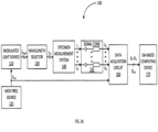
- FIG. 1A illustrates a block diagram of an exemplary optical signal processing system 100 in accordance with an aspect of the disclosure.
- the optical signal processing system 100 comprises: a light source configured to generate an incident light at a selected wavelength and amplitude modulated at a particular frequency; a specimen measurement system configured to direct the incident light at a specimen and generate a plurality of signals for measuring one or more characteristics of the specimen; a signal conditioner to generate suitable voltages for acquisition based on the signals generated by the specimen measurement system; a data acquisition circuit to substantially perform simultaneous sampling and digitizing of the voltages from the signal conditioner; and a software-based (SW-based) computing device configured to perform coherent detection and analysis of the digitized signals.
- SW-based software-based
- the simultaneous sampling and coherent detection of the signals allow the SW-based computing device to more accurately generate one or more measurements of the specimen in real-time. This is because the one or more measurements depend on a plurality of signals generated at substantially the same time. In other words, inaccuracy or noise due to time differences in the acquisition of the signals is minimized. Additionally, because a plurality of measurements depend on different sets of signals generated from the specimen measurement system, the simultaneous sampling and coherent detection ensures that different measurements are based on signals acquired at substantially the same time. Further, such different measurements may be accurately displayed simultaneously in real-time.
- the optical signal processing system 100 comprises a modulated light source 110, a modulation frequency source 120, a wavelength selector 130, a specimen measurement system 140, a signal conditioning circuit 150, a data acquisition circuit 160, and a SW-based computing device 170.
- the modulated light source 110 generates a modulated light with a defined range or bandwidth (bw) of wavelengths ⁇ bwf .
- modulated light source may include lasers, diodes, and other types of light sources.
- the modulated light source 110 generates the modulated light ⁇ bwf based on a modulation signal or voltage V mf , which cycles with a defined frequency (f).
- the modulation frequency source 120 generates the modulation signal or voltage V mf for the modulated light source 110.
- the wavelength selector 130 generates a modulated light with a selected wavelength ⁇ sf from the modulated light ⁇ bwf , wherein the selected wavelength ⁇ sf has a narrower band than the modulated light ⁇ bwf .
- the wavelength selector 130 may comprise a monochromator, filter, or other device capable of selecting a more narrowband wavelength within the wavelength range of the modulated light ⁇ bwf .
- the specimen measurement system 140 is configured to direct the selected modulated light ⁇ sf incident upon a specimen for measurement of one or more properties or characteristics of the specimen. In accordance with the measurement, the specimen measurement system 140 generates a plurality of electrical signals, such as currents I 1 to I N .
- the specimen measurement system 140 may generate a current I 1 related to the power level of the incident light ⁇ sf upon the specimen, and a current I 2 generated by the specimen in response to the incident light ⁇ sf .
- EQE extrinsic quantum efficiency
- the specimen measurement system 140 may generate a current I 1 related to the power level of the incident light ⁇ sf upon the specimen, a current I 2 related to a power level of specular light reflected by the specimen, a current I 3 related to a power level of diffusive light reflected by the specimen, and a current I4 generated by the specimen in response to the incident light ⁇ sf . It shall be understood that the specimen measurement system 140 may be configured to measure both EQE and I ⁇ aE, as well as perform other measurements on the specimen.
- IQE intrinsic quantum efficiency
- the signal conditioning circuit 150 performs transimpedance amplification and signal conditioning of the currents I 1 to I N to generate voltages V 1 to V N suitable for sampling and digitizing by the data acquisition circuit 160.
- the signal conditioning circuit 150 may perform the transimpedance amplification with a positive gain to generate the voltages V 1 to V N at suitable levels, and apply filtering and/or other processing to reduce noise.
- the data acquisition circuit 160 samples and digitizes the voltages V 1 to V N from the signal conditioning circuit 150 to generate digital signals D 1 to D N , respectively. Additionally, the data acquisition circuit 160 samples and digitizes the modulation voltage V mf from the modulation frequency source 120 to generate digital signal D mf . So that the coherent detection and any measurements performed by the SW-based computing device are based on the currents I 1 to I N derived at substantially the same time, the data acquisition circuit 160 is configured to simultaneously sample the voltages V 1 to V N and the modulation voltage V mf .
- the SW-based computing device 170 receives the digital signals D 1 to D N and D mf by way of any suitable digital interface, such as a Universal Serial Bus (USB) interface, Peripheral Component Interface (PCI), and others.
- the SW-based computing device may be any type of computing device, such as a desktop computer, laptop, smart phone, tablet-type computer, and others.
- the SW-based computing device 170 performs software-based coherent detection (also known as heterodyne or lock-in amplifier detection) to generate, potentially less-noisy, digital output signals related to the intensity or power level of the currents I 1 to I N generated at substantially the same time instance.
- the SW-based computing device 170 performs the coherent detection of the digital signals D 1 to D 5 in a manner that the resulting output signals are derived from the currents I 1 to I 5 at substantially the same time instance. This ensures time correlation for all the variables needed for the SW-based computing device 370 to derive the resulting one or more measurements (e.g., EQE and IQE) of the specimen.
- the SW-based computing device 170 may output the resulting one or more measurements, as well as the data derived from the specimen measurement system 140 and other associated data, to a user interface, such as a display, speakers, etc., to provide a user information related to the one or more measurements.
- a user interface such as a display, speakers, etc.
- the SW-based computing device 170 may receive instructions from a user as to how to perform the one or more measurements and how the information is provided to the user via the user interface.
- the SW-based computing device 170 may send control signals to any of the elements of the system 100 to configure the system in accordance with the user's inputs.
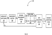
- FIG. 1B illustrates a block diagram of yet another exemplary optical signal processing system 105 in accordance with another aspect of the disclosure.
- the optical signal processing system 105 is a variation of the optical signal processing system 100 previously discussed, and includes many of the same elements as noted by the same reference numbers.
- the system 105 differs from system 100 in that the modulation signal or voltage V mf is generated internally within the data acquisition circuit 160, and not by an external modulation frequency source 120 as in system 100. Otherwise, the operation of the optical signal processing system 105 is substantially the same as optical signal processing system 100 previously discussed in detail.
- FIG. 1C illustrates a block diagram of an exemplary software-based coherent detection system implemented by the exemplary SW-based computing device 170 in accordance with another aspect of the disclosure.
- the system 170 comprises a SW-based phase lock loop (PLL) module 171, a SW-based frequency/harmonic (F/H) tone generator module 172, SW-based mixer modules 174-1 to 174-N, SW-based filter modules 176-1 to 176-N, and a SW-based processing module 178.
- the SW-based processing module 178 may interface with a control interface 180 for sending and/or receiving signals, such as control signals and sensed parameters, to and from other elements of the optical signal processing system 100 or 105. Additionally, the SW-based processing module 178 may interface with a user interface 190 for sending and/or receiving signals, such as measurement-related information and control signals, to and from a user of the optical signal processing system 100 or 105.
- PLL phase lock loop
- F/H frequency/harmonic
- the SW-based PLL module 171 is configured to generate a signal that is phase locked with the digital signal D mf . Since the digital signal D mf is derived from the modulation signal V mf , the signal generated by the SW-based PLL module 171 is phase locked with the modulation signal V mf . Based on a selected fundamental or harmonic command P, the SW-based F/H tone generator 172 may regenerate the fundamental signal D mf in the case P is equal to one (1), or may generate a desired harmonic P*D mf of the signal in the case P is an integer greater than one (1). The harmonic may be used to detect harmonic components of the modulation frequency in the digital signals D 1 to D N . Although not shown for simplicity sake, the output signal P*D mf of the SW-based F/H tone generator 172 includes both the sine and cosine components for proper heterodyne detection at the SW-based mixer modules 174-1 to 174-N.
- the selected tone P*D mf from the SW-based F/H tone generator 172 is applied to the SW-based mixer modules 174-1 to 174-N.
- the digital signals D 1 to D N are also applied to the SW-based mixer modules 174-1 to 174-N, respectively.
- the SW-based mixer modules 174-1 to 174-N mixes the digital signals D 1 to D N with the selected tone P*D mf to generate respective mixed signals.
- Each of the mixed signals includes a direct current (DC) carrier component and a sideband component.
- the sideband component may be associated with noise in the system 100 or 105.
- the corresponding SW-based filters 176-1 to 176-N substantially eliminate the sideband components of the mixed signals to generate output signals D O1 to D ON , respectively.
- the output signals D O1 to D ON are related to the power level or intensity of the signals or currents I 1 to I N generated by the specimen measurement system 140.
- the SW-based processing module 178 processes the output signals D O1 to D ON in accordance with the one or more desired measurements of one or more characteristics of the specimen. For example, if the optical signal processing system 100 or 105 is configured to measure EQE and/or IQE, the SW-based processing system 178 generates parameters indicative of the EQE and/or I ⁇ aE based on the output signals D O1 to D ON . The SW-based processing module 178 may send the measurement information to the user interface 190 to provide a user such information, in a graphical or non-graphical manner.
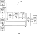
- FIG. 2A illustrates a block diagram of another exemplary optical signal processing system 200 in accordance with another aspect of the disclosure.
- the systems 100 and 105 were configured to generate an incident light for the specimen, whereby the incident light is configured with a selected wavelength and modulated at a particular frequency.
- the optical signal processing system 200 is configured to generate a combined incident light for the specimen, whereby the combined incident light is derived from a plurality of lights at different wavelengths and modulated with different frequencies.
- the optical signal processing system 200 comprises modulated light sources 210-1 to 210-M, modulation frequency sources 220-1 to 220-M, an optical combiner 230, a specimen measurement system 240, signal conditioning circuit 250, a data acquisition circuit 260, and a SW-based computing device 270.
- the modulated light sources 210-1 to 210-M generate lights ⁇ sf1 to ⁇ sfM configured with different wavelengths and modulated at different frequencies, respectively.
- the modulated light sources 210-1 to 210-M generate ⁇ sf1 to ⁇ sfM based on modulation signals or voltages V mf1 to V mfM generated by the modulation frequency sources 220-1 to 220-M, respectively.
- the modulation signals or voltages V mf1 to V mfM may be generated internally in the data acquisition circuit 260, as per optical signal processing system 105.
- the optical combiner 230 receive the respective lights ⁇ sf1 to ⁇ sfM from the modulated light sources 210-1 to 210-M, and combines them to generate a combined light ⁇ cb .
- the optical combiner 230 may be configured as a homogenizing rod/coupler or other type of optical signal combining device.
- the combined light ⁇ cb is provided to the specimen measurement system 240, which directs it incident upon a specimen.
- the specimen measurement system 240 generates a plurality of electrical signals I 1 to I N associated with the one or more measurements being performed on the specimen. Similar to the previous embodiments, the specimen measurement system 240 may be configured to generate electrical signals I 1 to I N pursuant to an EQE and/or I ⁇ aE measurement.
- the signal conditioning circuit 250 performs transimpedance amplification of the currents I 1 to I N and associated signal conditioning to generate corresponding voltages V 1 to V N suitable for sampling and digitizing by the data acquisition circuit 260.
- the data acquisition circuit 260 samples and digitizes the voltages V 1 to V N from the signal conditioning circuit 250 to generate digital signals D 1 to D N .
- the data acquisition circuit 260 also samples the modulation voltages V mf1 to V mfM from the modulation frequency sources 220-1 to 220-N to generate digital signals D mf1 to D mfM , respectively.
- the data acquisition circuit 260 simultaneously samples and digitizes the voltages V 1 to V N and V mf1 to V mfM so that the resulting measurement(s) generated by the SW-based computing device 270 are based on signals derived from the specimen at substantially the same time instance.
- the SW-based computing device 270 receives the digital signals D 1 to D N and D mf1 to D mfM via a digital interface (e.g., USB, PCI, etc).
- the SW-based computing device 270 performs coherent detection of the digital signals D 1 to D N using the modulation-based signals D mf1 to D mfM to generate output digital signals indicative of the intensity or power level of the currents I 1 to I N from the specimen measurement system 240.
- the SW-based computing device 270 performs the coherent detection of the digital signals D 1 to D 5 in a manner that the resulting output signals are derived from the currents I 1 to I 5 at substantially the same time instance. This ensures time correlation for all the variables needed for the SW-based computing device 270 to derive the resulting one or more measurements (e.g., EQE and IQE) of the specimen.
- FIG. 2B illustrates a block diagram of yet another exemplary optical signal processing system 205 in accordance with another aspect of the disclosure.
- the optical signal processing system 205 is a variation of the optical signal processing system 200, and includes many of the same elements as indicated by the same reference numbers.
- the optical signal processing system 205 differs from optical signal processing system 200 in that the modulated light sources 215-1 to 215-M may generate light signals ⁇ sf1 to ⁇ sfM with substantially the same wavelength, but modulated with different frequencies.
- the light signals ⁇ sf1 to ⁇ sfM are transmitted separately into the specimen measurement system 240.
- the specimen measurement system 240 directs the light signals ⁇ sf1 to ⁇ sfM at different regions of a specimen. This may be done to perform spatial analysis of the specimen.
- the resulting currents I 1 to I N generated by the specimen measurement system 240 may each have contributions from the light signals ⁇ sf1 to ⁇ sfM .
- the SW-based computing device 270 is capable of separating the contributions for individual analysis thereof.
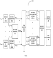
- FIG. 2C illustrates a block diagram of another exemplary software-based coherent detection system implemented by the exemplary SW-based computing device 270 in accordance with another aspect of the disclosure.
- the SW-based computing device 270 comprises a plurality of SW-based PLL modules 272-1 to 271-M, a plurality of F/H tone generator modules 272-1 to 272-M, and a beat tone generator module 273. Additionally, the SW-based computing device 270 further comprises a tone selector (mux) 274, a plurality of SW-based coherent or lock-in amplifier sections 275-1-N to 275-M-N, and a SW-based processing module 278.
- the SW based processing module 278 may interface with a control interface 280 for sending control signals and receiving sensed parameters, and may also interface with a user interface 290 for providing and receiving information to and from a user.
- the SW-based PLL modules 271-1 to 271-M generate signals phase locked with the digital signals D mf1 to D mfM , respectively.
- the beat tone generator module 273 generates a selected beat frequency signal D mf1 -D mfj based on a selected pair i and j of the phase locked signals generated from the SW-based PLL modules 271-1 to 271-M.
- the generated signals or tones P*D mf1 to P*D mfM and D mf1 -D mfj are provided to the tone selector module 274. Based on a user select signal (SEL), the tone selector module 274 outputs selected tones T 1 to T M .
- SEL user select signal
- the SW-based coherent or lock-in amplifier sections 275-1-N to 275-M-N use the selected tones T1 to TM to generate coherently-detected output signals D O11 to D OMN , respectively. For instance, if the fundamental frequencies D mf1 to D mfM are chosen for the selected tones T 1 to T M , then the output signals D O11 -D O1N to D OM1 -D OMN indicate the intensity or power level of the fundamental frequency components of the current signals I 1 to I N from the specimen measurement system 240, respectively.
- harmonic frequencies P*D mf1 to P*D mfM (P>1) are chosen for the selected tones T 1 to T M , then the output signals D O11 -D O1M to D OM1 -D OMN indicate the intensity or power level of the selected harmonic frequency components of the current signals I 1 to I N from the specimen measurement system 240, respectively.
- the output signals D O11 -D O1N to D OM1 -D OMN indicate the intensity or power level of the selected beat frequency component of the current signals I 1 to I N from the specimen measurement system 240, respectively.
- the optical signal processing system 300 comprises a modulated light source 310, a modulation frequency source 320, a wavelength selector 330, a light bias controller 315, an electrical bias controller 325, a specimen measurement system 340, a signal conditioning circuit 350, a data acquisition circuit 360, a SW-based computing device 370, and a user interface 390.
- the specimen measurement system 340 comprises a specular reflectance detector 341, a beam splitter 342, a diffusive device 343, a specimen 344, an X-Y stage 345, a reference detector 346, a diffusive reflectance detector 347, and an optical transmission detector 348.
- the modulated light source 310 is configured to generate a modulated light signal having a defined range of wavelengths ⁇ bwf .
- the modulated light source 310 is configured to generate the light signal ⁇ bwf based on a modulation signal or voltage V mf generated by the modulation frequency source 320.
- the wavelength selector 330 is configured to generate a modulated light signal having a selected wavelength ⁇ sf based on the light signal ⁇ bwf from the modulated light source 310, wherein the selected wavelength ⁇ sf has a narrower band than the modulated light ⁇ bwf .
- the wavelength selector 330 may comprise a monochromator, filter or other devices.
- the beam splitter 342 splits the light signal ⁇ sf into a reference signal and an incident signal.
- the reference signal is provided to the reference detector 346.
- the reference detector 346 In response to the reference signal, the reference detector 346 generates a current I 2 .
- the current I 2 is related (e.g., proportional) to the intensity or power level of the light source ⁇ sf .
- the incident signal is directed to the specimen 344 by way of the diffusive device 343.
- the diffusive device 343 may comprises an integration sphere or other type of diffusive device.
- the specimen 344 may generate a current I 5 in response to the diffusive incident light.
- the current I 5 may be used to determine the EQE and IQE, as well as other properties of the specimen 344.
- some of the incident light may pass or transmit through the specimen 344, which may be detected by optical transmission detector 348.
- the optical transmission detector 348 In response to the transmitted light, the optical transmission detector 348 generates a current I 4 .
- the current I 4 may be used to determine the EQE and IQE, as well as other properties of the specimen 344.
- the diffusive device 343 includes a port for outputting the diffusive reflected light.
- a diffusive reflectance detector 347 generates a current I 3 in response to the diffusive reflected light from the diffusive device 343.
- the current I 3 may be used to determine the EQE and IQE, as well as other properties of the specimen 344.
- some of the incident light reflected off of the specimen 344 at a normal angle, referred to herein as specular reflected light passes through the diffusive device 343 and the beam splitter 343, and is detected by the specular reflectance detector 341.
- the specular reflectance detector 341 generates a current I 1 in response to the specular reflected light.
- the current I 1 may be used to determine the EQE and IQE, as well as other properties of the specimen 344.
- the X-Y stage 345 of the specimen measurement system 340 supports the specimen 344, and facilitates the positioning of the specimen 344 either manually by a user or by way of an X-Y control signal generated by the SW-based computing device 370.
- the X-Y stage 345 may further include a sensor for generating a signal indicative of the temperature of the specimen.
- the X-Y stage 345 may provide the temperature signal to the SW-based computing device 370 via a control line.
- the light bias controller 315 of the optical signal processing system 300 may direct a controllable light at the specimen 344 in accordance with one or more measurements being made with regard to the specimen.
- the SW-based computing device 370 generates a control signal for the light bias controller 315.
- the electrical bias controller 325 may bias the specimen 344 with a controllable bias signal (e.g., a bias voltage and/or current) in accordance with one or more measurements being made with regard to the specimen.
- the SW-based computing device 370 generates a control signal for the electrical bias controller 325.
- the signal conditioning circuit 350 receives the currents I 1 to I 5 from the specimen measurement system 340 and generates therefrom respective voltages V 1 to V 5 suitable for sampling and digitizing by the data acquisition circuit 360.
- the data acquisition circuit 360 samples and digitizes the voltages V 1 to V 5 and the modulation frequency voltage V mf to generate digital signals D 1 to D 5 and D mf , respectively.
- the data acquisition circuit 360 samples these voltages in a substantially simultaneous manner.
- the SW-based computing device 370 performs the coherent detection of the digital signals D 1 to D 5 in a manner that the resulting output signals are derived from the currents I 1 to I 5 at substantially the same time instance. This ensures time correlation for all the variables needed for the SW-based computing device 370 to derive the EQE and IQE, as well as other properties of the specimen. As per the previous embodiments, the SW-based computing device 370 may provide and receive control-related signals to and from various elements of the optical signal processing system 300 per control lines indicated as alternate long- and-short-dashes. Additionally, the SW-based computing device 370 may provide and receive measurement-related information to and from a user via the user interface 390.
- FIG. 4 illustrates a block diagram of yet another exemplary optical signal processing system 400 in accordance with another aspect of the disclosure.
- the optical signal processing system 400 is an exemplary implementation of optical signal processing system 200 previously discussed, with a specimen measurement system being configured to measure EQE and/or IQE.
- the optical signal processing system 400 comprises modulated light sources 410-1 to 410-3, modulation frequency sources 420-1 to 420-3, an optical combiner 430, a light bias controller 415, an electrical bias controller 425, a specimen measurement system 440, a signal conditioning circuit 450, a data acquisition circuit 460, a SW-based computing device 470, and a user interface 490.
- Modulated light sources 420-1 to 420-3 are configured to generate modulated light signals having distinct selected wavelengths ⁇ sf1 , ⁇ sf2 , and ⁇ sf3 , and modulated with distinct frequencies based on modulation signals or voltages V mf1 , V mf2 and V mf3 generated by the modulation frequency sources 420-1, 420-2, and 420-3, respectively.
- the optical combiner 430 combines the modulated light signals ⁇ sf1 , ⁇ sf2 , and ⁇ sf3 to generate a combined light signal ⁇ cb .
- the specimen measurement system 440 uses the combined light signal ⁇ cb to generate an incident light for a specimen.
- the specimen measurement system 440 may be configured substantially the same or similar to specimen measurement system 340, previously discussed in detail.
- the specimen measurement system 440 generates currents I 1 to I 5 .
- the signal conditioner 450 performs transimpedance amplification and signal conditioning to convert the currents I 1 to I 5 into suitable voltages V 1 to V 5 for sampling and digitizing by the data acquisition circuit 460.
- the data acquisition circuit 460 samples and digitizes the voltages V 1 to V 5 and the modulation voltages V mf1 to V mf3 to generate digital signals D 1 to D 5 and D mf1 to D mf3 , respectively.
- the data acquisition circuit 460 samples and digitizes the signals in a substantially simultaneous manner.
- the SW-based computing device 470 performs coherent detection of the digital signals D 1 to D 5 using modulation signals D mf1 to D mf3 to generate output digital signals. If, for example, the coherent detection uses the fundamental tones D mf1 to D mf3 , the detected output signals indicate the intensity or power level of the fundamental frequency component of the currents I 1 to I 5 generated by the specimen measurement system 440. If, for example, the coherent detection uses harmonics P*D mf1 to P*D mf3 (P>1), the detected output signals indicate the intensity or power level of the corresponding harmonic frequency component of the currents I 1 to I 5 generated by the specimen measurement system 440.
- the detected output signals indicate the intensity or power level of the corresponding beat frequency component of the currents I 1 to I 5 generated by the specimen measurement system 440.
- the SW-based computing device 470 performs the coherent detection of the digital signals D 1 to D 5 in a manner that the resulting output signals are derived from the currents I 1 to I 5 at substantially the same time instance. This ensures time correlation for all the variables needed for the SW-based computing device 470 to derive the EQE and IQE, as well as other properties of the specimen. As per the previous embodiments, the SW-based computing device 470 may provide and receive control-related signals to and from various elements of the optical signal processing system 400 per control lines indicated as alternate long- and-short-dashes. Additionally, the SW-based computing device 470 may provide and receive measurement-related information to and from a user via the user interface 490.
- the light bias controller 415 of the optical signal processing system 400 directs controllable light at the specimen in accordance with one or more measurements being made with regard to the specimen.
- the SW-based computing device 470 generates a control signal for the light bias controller 415.
- the electrical bias controller 425 biases the specimen with a controllable bias signal (e.g., a bias voltage and/or current) in accordance with one or more measurements being made with regard to the specimen.
- the SW-based computing device 470 generates a control signal for the electrical bias controller 425.
- FIG. 5 illustrates a block diagram of still another exemplary optical signal processing system 500 in accordance with another aspect of the disclosure.
- the optical signal processing system 500 is an exemplary implementation of the optical signal processing system 205 previously discussed, with a specimen measurement system being configured to measure EQE and/or IQE.
- Modulated light sources 520-1 to 520-3 are configured to generate modulated light signals ⁇ sf1 , ⁇ sf2 , and ⁇ sf3 having substantially the same wavelength, but modulated with distinct frequencies based on modulation signals or voltages V mf1 , V mf2 and V mf3 generated by the modulation frequency sources 520-1, 520-2, and 520-3, respectively.
- the beam steering / programmable mask 530 is configured to direct the modulated light signals ⁇ sf1 , ⁇ sf2 , and ⁇ sf3 to desired regions of a specimen.
- the specimen measurement system 540 uses the modulated light signals ⁇ sf1 , ⁇ sf2 , and ⁇ sf3 to generate incident light signals for a specimen for spatial analysis thereof.
- the specimen measurement system 540 may be configured substantially the same or similar to specimen measurement system 340, previously discussed in detail.
- the specimen measurement system 540 generates currents I 1 to I 5 .
- the signal conditioning circuit 550 performs transimpedance amplification and signal conditioning to convert the currents I 1 to I 5 into suitable voltages V 1 to V 5 for sampling and digitizing by the data acquisition circuit 560.
- the data acquisition circuit 560 samples and digitizes the voltages V 1 to V 5 and the modulation voltages V mf1 to V mf3 to generate digital signals D 1 to D 5 and D mf1 to D mf3 , respectively.
- the data acquisition circuit 560 samples the signals in a substantially simultaneous manner.
- the SW-based computing device 570 performs the coherent detection of the digital signals D 1 to D 5 in a manner that the resulting output signals are derived from the currents I 1 to I 5 at substantially the same time instance. This ensures time correlation for all the variables needed for the SW-based computing device 570 to derive the EQE and IQE, as well as other properties of the specimen. As per the previous embodiments, the SW-based computing device 570 may provide and receive control-related signals to and from various elements of the optical measurement system 500 per control lines indicated as alternate long-and-short-dashes. Additionally, the SW-based computing device 570 may provide and receive measurement-related information to and from a user via the user interface 590.
- the light bias controller 515 of the optical measurement system 500 directs controllable light at the specimen in accordance with one or more measurement being made with regard to the specimen.
- the SW-based computing device 570 generates a control signal for the light bias controller 515.
- the electrical bias controller 425 biases the specimen with a controllable bias signal (e.g., a bias voltage and/or current) in accordance with one or more measurement being made with regard to the specimen.
- the SW-based computing device 570 generates a control signal for the electrical bias controller 525.
Landscapes
- Physics & Mathematics (AREA)
- Spectroscopy & Molecular Physics (AREA)
- General Physics & Mathematics (AREA)
- Biochemistry (AREA)
- Health & Medical Sciences (AREA)
- Life Sciences & Earth Sciences (AREA)
- Chemical & Material Sciences (AREA)
- Analytical Chemistry (AREA)
- General Health & Medical Sciences (AREA)
- Immunology (AREA)
- Pathology (AREA)
- Human Computer Interaction (AREA)
- Engineering & Computer Science (AREA)
- Investigating Or Analysing Materials By Optical Means (AREA)
Description
- This disclosure relates generally to optical systems, and in particular, to a system and method for coherently receiving simultaneous optical-based electrical signals.
- Optical measurement systems may be used to measure various parameters or characteristics of a specimen (e.g., a device-under-test (DUT) or sample material or component). Generally, an optical measurement system directs incident light at the specimen, and the specimen may produce polarized or unpolarized reflected light, polarized or unpolarized transmitted light, and electrical signal (e.g., current and voltage) in response to the stimulus. The optical measurement system typically includes devices to detect and analyze the reflected light, transmitted light, and/or electrical signal to measure the desired parameters or characteristics of the specimen.
- As an example, an optical measurement system for use in measuring the extrinsic quantum efficiency (EQE) of a specimen may include a light source (and other associated components) to generate and direct a defined incident light at the specimen. Such optical measurement system may also include a reference detector to detect a portion of the incident light, and an electrical detector to measure an electrical response (e.g., current or voltage) generated by the specimen in response to the stimuli. Such optical measurement system may include an analysis component to calculate the EQE of the specimen based on signals generated by the measurement system.
- Similarly, as another example, an optical measurement system for use in measuring the intrinsic quantum efficiency (IQE) may include a light source (and other associated components) to generate and direct a defined incident light at the specimen. Such optical measurement system may further include a reference detector to detect a portion of the incident light, a specular reflectance detector to detect light reflected at an angle from the specimen, a diffusive reflectance detector to detect scattered light reflected by the specimen, and an electrical detector to detect an electrical response (e.g., current or voltage) generated by the specimen in response to the stimuli. Such optical measurement system may include an analysis component to calculate the IQE of the specimen based on signals generated by the measurement system.
- Often, in the aforementioned optical measurement systems, significant noise may be present in the signals measured or generated by the detectors and specimen. In some cases, the noise is so prevalent that DC sampling the signals may not be possible or may result in erroneous detection. To combat noise, some optical measurement systems employ a dedicated lock-in amplifier to extract signals buried in noise. According to this technique, the intensity, frequency, or phase of the incident light is modulated at a frequency. The dedicated lock-in amplifier receives and mixes the detector signal with a signal with an established phase relationship with the modulation frequency (often referred to as coherent or heterodyne detection). The mixed signal is then passed through a filter to generate essentially the detector signal with reduced noise.
-
US2010219327A1 describes a high-speed Quantum Efficiency (QE) measurement device that includes at least one device under test (DUT), at least one conditioned light source having at least one filtered LED with a less than 50 nm bandwidth, where a portion of the conditioned light source is monitored by light source monitoring elements having at least one collection optic and at least one photo detector. The high-speed QE measurement device further includes delivery optics disposed to direct the conditioned light source to the DUT, a controller that drives the conditioned light source in a time dependent operation, where a response by each DUT from the conditioned light source is uniquely identified, and at least one reflectance measurement assembly having at least one reflectance collection optic and at least one photo detector disposed to receive a portion of the conditioned light that is reflected from the DUT. Additionally, the high-speed QE measurement device has a time-resolved measurement device that includes a current measurement device or a voltage measurement device, or a current measurement device and a voltage measurement device, where the time-resolved measurement device is disposed to resolve a current or a voltage, or a current and a voltage generated in the DUT by each conditioned light source. The high-speed QE measurement device further includes a sufficiently programmed computer disposed to determine and output an internal QE value for each DUT according to an incident intensity of at least one wavelength of from the conditioned light source and the time-resolved measurement.US8239165B discloses an apparatus for measuring quantum efficiency (QE) of solar cells. The apparatus includes a light source including an array of light emitting diodes (LEDs). Since all the LEDs can be power-modulated simultaneously and the corresponding cell responses to each of the LEDS can be analyzed simultaneously, the QE spectrum measurement time is greatly shortened as compared to conventional methods.DE3832906A describes a signal processing unit comprising a phase detection circuit which is contained in the signal processing circuit. Phase-sensitive detection for a photo-acoustic signal is carried out by using as a reference signal and a modulated signal which is fed from the current supply. - A drawback to such optical measurement systems is how task specific the dedicated lock-in amplifier are designed. This makes it difficult to re-configure the system and apply it towards measurements that do not require or cannot utilize lock-in functionality. An example would be in a system that is required to measure both the EQE and IΓaE of specimens that can or cannot respond to the frequency of modulation on the stimulating light source.
- The invention relates to systems according to
independent claims - An aspect of the disclosure relates to a system that may be configured to measure one or more properties of a specimen, such as the extrinsic quantum efficiency (EIaE), internal quantum efficiency (IQE), or other properties of the specimen. The system is configured to sample, digitize, and coherently detect signals from the specimen measurement system such that one or more resulting measurements are based on the signals acquired at substantially the same time instance. This facilitates the simultaneous calculation and presentation of the one or more resulting measurements in a real-time manner.
- In accordance with a first exemplary embodiment, the system comprises a modulation frequency source configured to generate a modulation frequency voltage; a modulated light source configured to generate a modulated light signal based on a modulation frequency voltage; a specimen measurement system configured to direct at least a portion of the modulated light signal incident upon a specimen for measurement of one or more properties of the specimen, wherein the specimen measurement system is configured to generate a plurality of measurement currents pursuant to the measurement of the one or more properties of the specimen; wherein the specimen measurement system, comprises a reference detector configured to generate a first current of the plurality of currents, the first current being related to an intensity of the incident light signal; a reflectance detector configured to generate a second current of the plurality of currents, the second current being related to an intensity of a light signal reflected by the specimen in response to the incident light signal; and a detector configured to generate a third current of the plurality of currents based on an electrical signal generated by the specimen in response to the incident light signal; a signal conditioner configured to generate a plurality of measurement voltages from the plurality of currents, respectively; a data acquisition circuit configured to: sample and digitize the plurality of measurement voltages to generate a plurality of measurement digital signals; receive the modulation frequency voltage from the modulation frequency source without the modulation frequency voltage being converted into optical domain; and sample and digitize the modulation frequency voltage to generate a reference digital signal, wherein the sampling of the measurement voltages and modulation frequency voltage are performed in a substantially simultaneous manner; and a computing device configured to perform software-based coherent detection of the measurement digital signals using the reference digital signal and.
- The system also comprises a data acquisition circuit configured to sample and digitize the plurality of measurement voltages to generate a plurality of measurement digital signals, and sample and digitize the modulation frequency voltage to generate a reference digital signal. The sampling of the measurement voltages and modulation frequency voltage is performed in a substantially simultaneous manner. The simultaneous sampling ensures that the one or more resulting measurements, such as EQE and IΓaE, are based on the currents generated by the specimen measurement system generated at substantially the same time instance. The system comprises a computing device configured to perform software-based coherent detection of the measurement digital signals using the reference digital signal.
- In accordance with one embodiment, the computing device may be configured to perform the coherent detection of the measurement digital signals by at least mixing the measurement digital signals with a mixing signal based on the reference digital signal to generate a plurality of respective mixed digital signals, and filtering the digital mixed signals to generate output digital signals. In accordance with another embodiment, the mixing signal may be related to a frequency harmonic of the reference digital signal. Additionally, the computing device may be configured to generate one or more indications of the one or more properties of the specimen based on the output digital signals. Such one or more indications may include the EQE, IΓaE, or other one or more properties of the specimen.
- In accordance with the first embodiment, the specimen measurement system comprises a reference detector configured to generate a first current of the plurality of currents, the first current being related to an intensity of the incident light signal, and wherein a second current of the plurality of currents is generated by the specimen in response to the incident light signal. Alternatively, the specimen measurement system comprises a reference detector configured to generate a first current of the plurality of currents, the first current being related to an intensity of the incident light signal, a reflectance detector configured to generate a second current of the plurality of currents, the second current being related to the intensity of a light signal being reflected by the specimen in response to the incident light signal, and a detector configured to generate a third current of the plurality of currents based on an electrical signal generated by the specimen in response to the incident light signal.
- In accordance with a second exemplary embodiment, the system comprises a light source configured to generate a distinct band of wavelength light signals being modulated based on respective distinct modulation frequency voltages; an optical combiner configured to generate a combined light signal based on the distinct band of wavelengths modulated light signals; and a specimen measurement system configured to direct at least a portion of the combined light signal incident upon a specimen for measurement of one or more properties of the specimen, wherein the specimen measurement system is configured to generate a plurality of measurement currents pursuant to the measurement of the one or more properties of the specimen.
- In accordance with the second embodiment, the system comprises a signal conditioner configured to generate a plurality of measurement voltages from the plurality of currents, respectively. Further, the system comprises a data acquisition circuit configured to sample and digitize the plurality of measurement voltages to generate a plurality of measurement digital signals, and sample and digitize the plurality of modulation frequency voltages to generate a plurality of reference digital signals. The sampling of the measurement voltages and the modulation frequency voltages are performed in a substantially simultaneous manner. Additionally, the system comprises a computing device configured to perform software-based coherent detection of the measurement digital signals using the reference digital signals.
- The computing device may be configured to perform the coherent detection of the measurement digital signals by mixing the measurement digital signals with mixing signals based on the reference digital signals to generate a plurality of mixed digital signals, and filtering the digital mixed signals to generate output digital signals. In one aspect, the mixing signals are related to frequency harmonics of the reference digital signals, respectively. In another aspect, the mixing signals are related to one or more beat frequencies each based on one or more selected pairs of the reference digital signals.
- As per the first exemplary embodiment, the computing device is configured to generate one or more indications of the one or more properties of the specimen based on the output digital signals, such as EQE, IQE, or any other one or more properties of the specimen. As per the first exemplary embodiment, the specimen measurement system may be configured to include a reference detector, a reflectance detector, as well as other detectors, and configured to produce the current generated by the specimen in response to the incident light.
- In accordance with a third exemplary embodiment, the system comprises a light source configured to generate a plurality of light signals modulated based on a plurality of distinct modulation frequency voltages, respectively; a specimen measurement system configured to direct portions of the plurality of light signals incident upon distinct regions of a specimen for measurement of one or more properties of the specimen, wherein the specimen measurement system is configured to generate a plurality of measurement currents pursuant to the measurement of the one or more properties of the specimen; and a signal conditioner configured to generate a plurality of measurement voltages from the plurality of measurement currents, respectively.
- Additionally, in accordance with the third exemplary embodiment, the system comprises a data acquisition circuit configured to sample and digitize the plurality of measurement voltages to generate a plurality of measurement digital signals, and sample and digitize the plurality of modulation frequency voltages to generate a plurality of reference digital signals. The sampling of the measurement voltages and the modulation frequency voltages are performed in a substantially simultaneous manner. In addition, the system comprises a computing device configured to perform software-based coherent detection of the measurement digital signals using the reference digital signals. Other elements of the third embodiment may be configured substantially the same or similar to the second embodiment.
- Other aspects, advantages and novel features of the disclosure will become apparent from the following detailed description of the invention when considered in conjunction with the accompanying drawings.
-
-
FIG. 1A illustrates a block diagram of an exemplary optical signal processing system in accordance with an aspect of the disclosure. -
FIG. 1B illustrates a block diagram of yet another exemplary optical signal processing system in accordance with another aspect of the disclosure. -
FIG. 1C illustrates a block diagram of an exemplary software-based coherent detection system in accordance with another aspect of the disclosure. -
FIG. 2A illustrates a block diagram of another exemplary optical signal processing system in accordance with an aspect of the disclosure. -
FIG. 2B illustrates a block diagram of yet another exemplary optical signal processing system in accordance with another aspect of the disclosure. -
FIG. 2C illustrates a block diagram of another exemplary software-based coherent detection system in accordance with another aspect of the disclosure. -
FIG. 3 illustrates a block diagram of another exemplary optical signal processing system in accordance with another aspect of the disclosure. -
FIG. 4 illustrates a block diagram of yet another exemplary optical signal processing system in accordance with another aspect of the disclosure. -
FIG. 5 illustrates a block diagram of still another exemplary optical signal processing system in accordance with another aspect of the disclosure. -
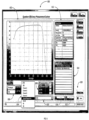
FIG. 6 illustrates a screen shot of an exemplary graphical user interface (GUI) generated by an exemplary user interface in accordance with another aspect of the disclosure. -
FIG. 1A illustrates a block diagram of an exemplary opticalsignal processing system 100 in accordance with an aspect of the disclosure. In summary, the opticalsignal processing system 100 comprises: a light source configured to generate an incident light at a selected wavelength and amplitude modulated at a particular frequency; a specimen measurement system configured to direct the incident light at a specimen and generate a plurality of signals for measuring one or more characteristics of the specimen; a signal conditioner to generate suitable voltages for acquisition based on the signals generated by the specimen measurement system; a data acquisition circuit to substantially perform simultaneous sampling and digitizing of the voltages from the signal conditioner; and a software-based (SW-based) computing device configured to perform coherent detection and analysis of the digitized signals. - The simultaneous sampling and coherent detection of the signals allow the SW-based computing device to more accurately generate one or more measurements of the specimen in real-time. This is because the one or more measurements depend on a plurality of signals generated at substantially the same time. In other words, inaccuracy or noise due to time differences in the acquisition of the signals is minimized. Additionally, because a plurality of measurements depend on different sets of signals generated from the specimen measurement system, the simultaneous sampling and coherent detection ensures that different measurements are based on signals acquired at substantially the same time. Further, such different measurements may be accurately displayed simultaneously in real-time.
- More specifically, the optical
signal processing system 100 comprises a modulatedlight source 110, amodulation frequency source 120, awavelength selector 130, aspecimen measurement system 140, asignal conditioning circuit 150, adata acquisition circuit 160, and a SW-basedcomputing device 170. - The modulated
light source 110 generates a modulated light with a defined range or bandwidth (bw) of wavelengths λbwf. Examples of modulated light source may include lasers, diodes, and other types of light sources. The modulatedlight source 110 generates the modulated light λbwf based on a modulation signal or voltage Vmf, which cycles with a defined frequency (f). Themodulation frequency source 120 generates the modulation signal or voltage Vmf for the modulatedlight source 110. Thewavelength selector 130 generates a modulated light with a selected wavelength λsf from the modulated light λbwf, wherein the selected wavelength λsf has a narrower band than the modulated light λbwf. Thewavelength selector 130 may comprise a monochromator, filter, or other device capable of selecting a more narrowband wavelength within the wavelength range of the modulated light λbwf. - The
specimen measurement system 140 is configured to direct the selected modulated light λsf incident upon a specimen for measurement of one or more properties or characteristics of the specimen. In accordance with the measurement, thespecimen measurement system 140 generates a plurality of electrical signals, such as currents I1 to IN. - For example, if the
specimen measurement system 140 is configured to measure the extrinsic quantum efficiency (EQE) of a specimen, thespecimen measurement system 140 may generate a current I1 related to the power level of the incident light λsf upon the specimen, and a current I2 generated by the specimen in response to the incident light λsf. If thespecimen measurement system 140 is configured to measure the intrinsic quantum efficiency (IQE) of a specimen, thespecimen measurement system 140 may generate a current I1 related to the power level of the incident light λsf upon the specimen, a current I2 related to a power level of specular light reflected by the specimen, a current I3 related to a power level of diffusive light reflected by the specimen, and a current I4 generated by the specimen in response to the incident light λsf. It shall be understood that thespecimen measurement system 140 may be configured to measure both EQE and IΓaE, as well as perform other measurements on the specimen. - The
signal conditioning circuit 150 performs transimpedance amplification and signal conditioning of the currents I1 to IN to generate voltages V1 to VN suitable for sampling and digitizing by thedata acquisition circuit 160. For example, thesignal conditioning circuit 150 may perform the transimpedance amplification with a positive gain to generate the voltages V1 to VN at suitable levels, and apply filtering and/or other processing to reduce noise. - As previously discussed the
data acquisition circuit 160 samples and digitizes the voltages V1 to VN from thesignal conditioning circuit 150 to generate digital signals D1 to DN, respectively. Additionally, thedata acquisition circuit 160 samples and digitizes the modulation voltage Vmf from themodulation frequency source 120 to generate digital signal Dmf. So that the coherent detection and any measurements performed by the SW-based computing device are based on the currents I1 to IN derived at substantially the same time, thedata acquisition circuit 160 is configured to simultaneously sample the voltages V1 to VN and the modulation voltage Vmf. - The SW-based
computing device 170 receives the digital signals D1 to DN and Dmf by way of any suitable digital interface, such as a Universal Serial Bus (USB) interface, Peripheral Component Interface (PCI), and others. The SW-based computing device may be any type of computing device, such as a desktop computer, laptop, smart phone, tablet-type computer, and others. As discussed in more detail herein, the SW-basedcomputing device 170 performs software-based coherent detection (also known as heterodyne or lock-in amplifier detection) to generate, potentially less-noisy, digital output signals related to the intensity or power level of the currents I1 to IN generated at substantially the same time instance. The SW-basedcomputing device 170 performs the coherent detection of the digital signals D1 to D5 in a manner that the resulting output signals are derived from the currents I1 to I5 at substantially the same time instance. This ensures time correlation for all the variables needed for the SW-basedcomputing device 370 to derive the resulting one or more measurements (e.g., EQE and IQE) of the specimen. - Additionally, the SW-based
computing device 170 may output the resulting one or more measurements, as well as the data derived from thespecimen measurement system 140 and other associated data, to a user interface, such as a display, speakers, etc., to provide a user information related to the one or more measurements. Via the user interface, as in the case of input devices such as a keyboard, mouse, microphones, etc., the SW-basedcomputing device 170 may receive instructions from a user as to how to perform the one or more measurements and how the information is provided to the user via the user interface. In this regards, the SW-basedcomputing device 170 may send control signals to any of the elements of thesystem 100 to configure the system in accordance with the user's inputs. -
FIG. 1B illustrates a block diagram of yet another exemplary opticalsignal processing system 105 in accordance with another aspect of the disclosure. The opticalsignal processing system 105 is a variation of the opticalsignal processing system 100 previously discussed, and includes many of the same elements as noted by the same reference numbers. Thesystem 105 differs fromsystem 100 in that the modulation signal or voltage Vmf is generated internally within thedata acquisition circuit 160, and not by an externalmodulation frequency source 120 as insystem 100. Otherwise, the operation of the opticalsignal processing system 105 is substantially the same as opticalsignal processing system 100 previously discussed in detail. -
FIG. 1C illustrates a block diagram of an exemplary software-based coherent detection system implemented by the exemplary SW-basedcomputing device 170 in accordance with another aspect of the disclosure. Thesystem 170 comprises a SW-based phase lock loop (PLL)module 171, a SW-based frequency/harmonic (F/H)tone generator module 172, SW-based mixer modules 174-1 to 174-N, SW-based filter modules 176-1 to 176-N, and a SW-basedprocessing module 178. The SW-basedprocessing module 178 may interface with acontrol interface 180 for sending and/or receiving signals, such as control signals and sensed parameters, to and from other elements of the opticalsignal processing system processing module 178 may interface with auser interface 190 for sending and/or receiving signals, such as measurement-related information and control signals, to and from a user of the opticalsignal processing system - The SW-based
PLL module 171 is configured to generate a signal that is phase locked with the digital signal Dmf. Since the digital signal Dmf is derived from the modulation signal Vmf, the signal generated by the SW-basedPLL module 171 is phase locked with the modulation signal Vmf. Based on a selected fundamental or harmonic command P, the SW-based F/H tone generator 172 may regenerate the fundamental signal Dmf in the case P is equal to one (1), or may generate a desired harmonic P*Dmf of the signal in the case P is an integer greater than one (1). The harmonic may be used to detect harmonic components of the modulation frequency in the digital signals D1 to DN. Although not shown for simplicity sake, the output signal P*Dmf of the SW-based F/H tone generator 172 includes both the sine and cosine components for proper heterodyne detection at the SW-based mixer modules 174-1 to 174-N. - As mentioned, the selected tone P*Dmf from the SW-based F/
H tone generator 172 is applied to the SW-based mixer modules 174-1 to 174-N. The digital signals D1 to DN are also applied to the SW-based mixer modules 174-1 to 174-N, respectively. The SW-based mixer modules 174-1 to 174-N mixes the digital signals D1 to DN with the selected tone P*Dmf to generate respective mixed signals. Each of the mixed signals includes a direct current (DC) carrier component and a sideband component. The sideband component may be associated with noise in thesystem specimen measurement system 140. - The SW-based
processing module 178 processes the output signals DO1 to DON in accordance with the one or more desired measurements of one or more characteristics of the specimen. For example, if the opticalsignal processing system processing system 178 generates parameters indicative of the EQE and/or IΓaE based on the output signals DO1 to DON. The SW-basedprocessing module 178 may send the measurement information to theuser interface 190 to provide a user such information, in a graphical or non-graphical manner. -
FIG. 2A illustrates a block diagram of another exemplary opticalsignal processing system 200 in accordance with another aspect of the disclosure. In the previous exemplary embodiments, thesystems signal processing system 200 is configured to generate a combined incident light for the specimen, whereby the combined incident light is derived from a plurality of lights at different wavelengths and modulated with different frequencies. - More specifically, the optical
signal processing system 200 comprises modulated light sources 210-1 to 210-M, modulation frequency sources 220-1 to 220-M, anoptical combiner 230, aspecimen measurement system 240,signal conditioning circuit 250, adata acquisition circuit 260, and a SW-basedcomputing device 270. - The modulated light sources 210-1 to 210-M generate lights λsf1 to λsfM configured with different wavelengths and modulated at different frequencies, respectively. The modulated light sources 210-1 to 210-M generate λsf1 to λsfM based on modulation signals or voltages Vmf1 to VmfM generated by the modulation frequency sources 220-1 to 220-M, respectively. Alternatively, instead of the external modulation frequency sources 220-1 to 220-M, the modulation signals or voltages Vmf1 to VmfM may be generated internally in the
data acquisition circuit 260, as per opticalsignal processing system 105. - The
optical combiner 230 receive the respective lights λsf1 to λsfM from the modulated light sources 210-1 to 210-M, and combines them to generate a combined light λcb. As an example, theoptical combiner 230 may be configured as a homogenizing rod/coupler or other type of optical signal combining device. The combined light λcb is provided to thespecimen measurement system 240, which directs it incident upon a specimen. As per the previousspecimen measurement system 140, thespecimen measurement system 240 generates a plurality of electrical signals I1 to IN associated with the one or more measurements being performed on the specimen. Similar to the previous embodiments, thespecimen measurement system 240 may be configured to generate electrical signals I1 to IN pursuant to an EQE and/or IΓaE measurement. - Similar to the previous embodiments, the
signal conditioning circuit 250 performs transimpedance amplification of the currents I1 to IN and associated signal conditioning to generate corresponding voltages V1 to VN suitable for sampling and digitizing by thedata acquisition circuit 260. - The
data acquisition circuit 260 samples and digitizes the voltages V1 to VN from thesignal conditioning circuit 250 to generate digital signals D1 to DN. Thedata acquisition circuit 260 also samples the modulation voltages Vmf1 to VmfM from the modulation frequency sources 220-1 to 220-N to generate digital signals Dmf1 to DmfM, respectively. As per the previous embodiments, thedata acquisition circuit 260 simultaneously samples and digitizes the voltages V1 to VN and Vmf1 to VmfM so that the resulting measurement(s) generated by the SW-basedcomputing device 270 are based on signals derived from the specimen at substantially the same time instance. - As per the previous embodiments, the SW-based
computing device 270 receives the digital signals D1 to DN and Dmf1 to DmfM via a digital interface (e.g., USB, PCI, etc). The SW-basedcomputing device 270 performs coherent detection of the digital signals D1 to DN using the modulation-based signals Dmf1 to DmfM to generate output digital signals indicative of the intensity or power level of the currents I1 to IN from thespecimen measurement system 240. The SW-basedcomputing device 270 performs the coherent detection of the digital signals D1 to D5 in a manner that the resulting output signals are derived from the currents I1 to I5 at substantially the same time instance. This ensures time correlation for all the variables needed for the SW-basedcomputing device 270 to derive the resulting one or more measurements (e.g., EQE and IQE) of the specimen. -
FIG. 2B illustrates a block diagram of yet another exemplary opticalsignal processing system 205 in accordance with another aspect of the disclosure. The opticalsignal processing system 205 is a variation of the opticalsignal processing system 200, and includes many of the same elements as indicated by the same reference numbers. The opticalsignal processing system 205 differs from opticalsignal processing system 200 in that the modulated light sources 215-1 to 215-M may generate light signals λsf1 to λsfM with substantially the same wavelength, but modulated with different frequencies. - Another difference is that the light signals λsf1 to λsfM are transmitted separately into the
specimen measurement system 240. Thespecimen measurement system 240 directs the light signals λsf1 to λsfM at different regions of a specimen. This may be done to perform spatial analysis of the specimen. The resulting currents I1 to IN generated by thespecimen measurement system 240 may each have contributions from the light signals λsf1 to λsfM. Using coherent detection, the SW-basedcomputing device 270 is capable of separating the contributions for individual analysis thereof. -
FIG. 2C illustrates a block diagram of another exemplary software-based coherent detection system implemented by the exemplary SW-basedcomputing device 270 in accordance with another aspect of the disclosure. The SW-basedcomputing device 270 comprises a plurality of SW-based PLL modules 272-1 to 271-M, a plurality of F/H tone generator modules 272-1 to 272-M, and a beattone generator module 273. Additionally, the SW-basedcomputing device 270 further comprises a tone selector (mux) 274, a plurality of SW-based coherent or lock-in amplifier sections 275-1-N to 275-M-N, and a SW-basedprocessing module 278. As per the previous embodiments, the SW basedprocessing module 278 may interface with acontrol interface 280 for sending control signals and receiving sensed parameters, and may also interface with auser interface 290 for providing and receiving information to and from a user. - The SW-based PLL modules 271-1 to 271-M generate signals phase locked with the digital signals Dmf1 to DmfM, respectively. The F/H tone generator modules 272-1 to 272-M generate fundamental (P=1) or harmonics (P > 1) signals P*Dmf1 to P*DmfM based on user selected parameter P, respectively. The beat
tone generator module 273 generates a selected beat frequency signal Dmf1-Dmfj based on a selected pair i and j of the phase locked signals generated from the SW-based PLL modules 271-1 to 271-M. The generated signals or tones P*Dmf1 to P*DmfM and Dmf1-Dmfj are provided to thetone selector module 274. Based on a user select signal (SEL), thetone selector module 274 outputs selected tones T1 to TM. - The SW-based coherent or lock-in amplifier sections 275-1-N to 275-M-N use the selected tones T1 to TM to generate coherently-detected output signals DO11 to DOMN, respectively. For instance, if the fundamental frequencies Dmf1 to DmfM are chosen for the selected tones T1 to TM, then the output signals DO11-DO1N to DOM1-DOMN indicate the intensity or power level of the fundamental frequency components of the current signals I1 to IN from the
specimen measurement system 240, respectively. If harmonic frequencies P*Dmf1 to P*DmfM (P>1) are chosen for the selected tones T1 to TM, then the output signals DO11-DO1M to DOM1-DOMN indicate the intensity or power level of the selected harmonic frequency components of the current signals I1 to IN from thespecimen measurement system 240, respectively. Similarly, if a certain beat frequency is chosen for the selected tones T1 to TM, then the output signals DO11-DO1N to DOM1-DOMN indicate the intensity or power level of the selected beat frequency component of the current signals I1 to IN from thespecimen measurement system 240, respectively. - The SW-based
processing module 278 processes the output signals DO11-DOIN to DOM1-DOMN in accordance with the one or more desired measurements of one or more characteristics of the specimen. For example, if the opticalsignal processing system processing system 278 generates parameters indicative of the EQE and/or IΓaE based on the output signals DO11-DO1N to DOM1-DOMN. The SW-basedprocessing module 278 may send the measurement information to theuser interface 290 to provide a user such information, in a graphical or non-graphical manner. -
FIG. 3 illustrates a block diagram of another exemplary opticalsignal processing system 300 in accordance with another aspect of the disclosure. The opticalsignal processing system 300 is an exemplary implementation of opticalsignal processing system 100 previously discussed, with a specimen measurement system being configured to measure EQE and/or IQE. - In particular, the optical
signal processing system 300 comprises a modulatedlight source 310, amodulation frequency source 320, awavelength selector 330, alight bias controller 315, anelectrical bias controller 325, aspecimen measurement system 340, asignal conditioning circuit 350, adata acquisition circuit 360, a SW-basedcomputing device 370, and auser interface 390. Thespecimen measurement system 340, in turn, comprises aspecular reflectance detector 341, abeam splitter 342, adiffusive device 343, aspecimen 344, anX-Y stage 345, areference detector 346, adiffusive reflectance detector 347, and anoptical transmission detector 348. - The modulated
light source 310 is configured to generate a modulated light signal having a defined range of wavelengths λbwf. The modulatedlight source 310 is configured to generate the light signal λbwf based on a modulation signal or voltage Vmf generated by themodulation frequency source 320. Thewavelength selector 330 is configured to generate a modulated light signal having a selected wavelength λsf based on the light signal λbwf from the modulatedlight source 310, wherein the selected wavelength λsf has a narrower band than the modulated light λbwf. As previously discussed with reference tosystem 100, thewavelength selector 330 may comprise a monochromator, filter or other devices. - With regard to the
specimen measurement system 340, thebeam splitter 342 splits the light signal λsf into a reference signal and an incident signal. The reference signal is provided to thereference detector 346. In response to the reference signal, thereference detector 346 generates a current I2. The current I2 is related (e.g., proportional) to the intensity or power level of the light source λsf. The incident signal is directed to thespecimen 344 by way of thediffusive device 343. Thediffusive device 343 may comprises an integration sphere or other type of diffusive device. - The
specimen 344 may generate a current I5 in response to the diffusive incident light. The current I5 may be used to determine the EQE and IQE, as well as other properties of thespecimen 344. In some cases, some of the incident light may pass or transmit through thespecimen 344, which may be detected byoptical transmission detector 348. In response to the transmitted light, theoptical transmission detector 348 generates a current I4. The current I4 may be used to determine the EQE and IQE, as well as other properties of thespecimen 344. - Some of the incident light is reflected off of the
specimen 344. The reflected light is received by thediffusive device 343. Thediffusive device 343 includes a port for outputting the diffusive reflected light. Adiffusive reflectance detector 347 generates a current I3 in response to the diffusive reflected light from thediffusive device 343. The current I3 may be used to determine the EQE and IQE, as well as other properties of thespecimen 344. Additionally, some of the incident light reflected off of thespecimen 344 at a normal angle, referred to herein as specular reflected light, passes through thediffusive device 343 and thebeam splitter 343, and is detected by thespecular reflectance detector 341. Thespecular reflectance detector 341 generates a current I1 in response to the specular reflected light. The current I1 may be used to determine the EQE and IQE, as well as other properties of thespecimen 344. - The
X-Y stage 345 of thespecimen measurement system 340 supports thespecimen 344, and facilitates the positioning of thespecimen 344 either manually by a user or by way of an X-Y control signal generated by the SW-basedcomputing device 370. TheX-Y stage 345 may further include a sensor for generating a signal indicative of the temperature of the specimen. TheX-Y stage 345 may provide the temperature signal to the SW-basedcomputing device 370 via a control line. - The
light bias controller 315 of the opticalsignal processing system 300 may direct a controllable light at thespecimen 344 in accordance with one or more measurements being made with regard to the specimen. In this regards, the SW-basedcomputing device 370 generates a control signal for thelight bias controller 315. Additionally, theelectrical bias controller 325 may bias thespecimen 344 with a controllable bias signal (e.g., a bias voltage and/or current) in accordance with one or more measurements being made with regard to the specimen. In this regards, the SW-basedcomputing device 370 generates a control signal for theelectrical bias controller 325. - As per the previous embodiments, the
signal conditioning circuit 350 receives the currents I1 to I5 from thespecimen measurement system 340 and generates therefrom respective voltages V1 to V5 suitable for sampling and digitizing by thedata acquisition circuit 360. As per the previous embodiments, thedata acquisition circuit 360 samples and digitizes the voltages V1 to V5 and the modulation frequency voltage Vmf to generate digital signals D1 to D5 and Dmf, respectively. As per the previous embodiment, thedata acquisition circuit 360 samples these voltages in a substantially simultaneous manner. - The SW-based
computing device 370 performs the coherent detection of the digital signals D1 to D5 in a manner that the resulting output signals are derived from the currents I1 to I5 at substantially the same time instance. This ensures time correlation for all the variables needed for the SW-basedcomputing device 370 to derive the EQE and IQE, as well as other properties of the specimen. As per the previous embodiments, the SW-basedcomputing device 370 may provide and receive control-related signals to and from various elements of the opticalsignal processing system 300 per control lines indicated as alternate long- and-short-dashes. Additionally, the SW-basedcomputing device 370 may provide and receive measurement-related information to and from a user via theuser interface 390. -
FIG. 4 illustrates a block diagram of yet another exemplary opticalsignal processing system 400 in accordance with another aspect of the disclosure. The opticalsignal processing system 400 is an exemplary implementation of opticalsignal processing system 200 previously discussed, with a specimen measurement system being configured to measure EQE and/or IQE. - In particular, the optical
signal processing system 400 comprises modulated light sources 410-1 to 410-3, modulation frequency sources 420-1 to 420-3, anoptical combiner 430, alight bias controller 415, anelectrical bias controller 425, aspecimen measurement system 440, asignal conditioning circuit 450, adata acquisition circuit 460, a SW-basedcomputing device 470, and auser interface 490. - Modulated light sources 420-1 to 420-3 are configured to generate modulated light signals having distinct selected wavelengths λsf1, λsf2, and λsf3, and modulated with distinct frequencies based on modulation signals or voltages Vmf1, Vmf2 and Vmf3 generated by the modulation frequency sources 420-1, 420-2, and 420-3, respectively. The
optical combiner 430 combines the modulated light signals λsf1, λsf2, and λsf3 to generate a combined light signal λcb. Thespecimen measurement system 440 uses the combined light signal λcb to generate an incident light for a specimen. Thespecimen measurement system 440 may be configured substantially the same or similar tospecimen measurement system 340, previously discussed in detail. - As per the previous embodiment, the
specimen measurement system 440 generates currents I1 to I5. Thesignal conditioner 450 performs transimpedance amplification and signal conditioning to convert the currents I1 to I5 into suitable voltages V1 to V5 for sampling and digitizing by thedata acquisition circuit 460. As per the previous embodiments, thedata acquisition circuit 460 samples and digitizes the voltages V1 to V5 and the modulation voltages Vmf1 to Vmf3 to generate digital signals D1 to D5 and Dmf1 to Dmf3, respectively. Thedata acquisition circuit 460 samples and digitizes the signals in a substantially simultaneous manner. - As per SW-based
computing device 270 previously discussed, the SW-basedcomputing device 470 performs coherent detection of the digital signals D1 to D5 using modulation signals Dmf1 to Dmf3 to generate output digital signals. If, for example, the coherent detection uses the fundamental tones Dmf1 to Dmf3, the detected output signals indicate the intensity or power level of the fundamental frequency component of the currents I1 to I5 generated by thespecimen measurement system 440. If, for example, the coherent detection uses harmonics P*Dmf1 to P*Dmf3 (P>1), the detected output signals indicate the intensity or power level of the corresponding harmonic frequency component of the currents I1 to I5 generated by thespecimen measurement system 440. If, for example, the coherent detection uses a selected beat frequency (Dmfi ± Dmfj)(i≠j, i=j={1,2,3}), the detected output signals indicate the intensity or power level of the corresponding beat frequency component of the currents I1 to I5 generated by thespecimen measurement system 440. - The SW-based
computing device 470 performs the coherent detection of the digital signals D1 to D5 in a manner that the resulting output signals are derived from the currents I1 to I5 at substantially the same time instance. This ensures time correlation for all the variables needed for the SW-basedcomputing device 470 to derive the EQE and IQE, as well as other properties of the specimen. As per the previous embodiments, the SW-basedcomputing device 470 may provide and receive control-related signals to and from various elements of the opticalsignal processing system 400 per control lines indicated as alternate long- and-short-dashes. Additionally, the SW-basedcomputing device 470 may provide and receive measurement-related information to and from a user via theuser interface 490. - As per the previous embodiment, the
light bias controller 415 of the opticalsignal processing system 400 directs controllable light at the specimen in accordance with one or more measurements being made with regard to the specimen. In this regards, the SW-basedcomputing device 470 generates a control signal for thelight bias controller 415. Theelectrical bias controller 425 biases the specimen with a controllable bias signal (e.g., a bias voltage and/or current) in accordance with one or more measurements being made with regard to the specimen. In this regards, the SW-basedcomputing device 470 generates a control signal for theelectrical bias controller 425. -
FIG. 5 illustrates a block diagram of still another exemplary opticalsignal processing system 500 in accordance with another aspect of the disclosure. The opticalsignal processing system 500 is an exemplary implementation of the opticalsignal processing system 205 previously discussed, with a specimen measurement system being configured to measure EQE and/or IQE. - In particular, the optical
signal processing system 500 comprises modulated light sources 510-1 to 510-3, modulation frequency sources 520-1 to 520-3, beam steering orprogrammable mask 530, alight bias controller 515, anelectrical bias controller 525, aspecimen measurement system 540, asignal conditioning circuit 550, adata acquisition circuit 560, a SW-basedcomputing device 570, and a user interface 590. - Modulated light sources 520-1 to 520-3 are configured to generate modulated light signals λsf1, λsf2, and λsf3 having substantially the same wavelength, but modulated with distinct frequencies based on modulation signals or voltages Vmf1, Vmf2 and Vmf3 generated by the modulation frequency sources 520-1, 520-2, and 520-3, respectively. The beam steering /
programmable mask 530 is configured to direct the modulated light signals λsf1, λsf2, and λsf3 to desired regions of a specimen. Thespecimen measurement system 540 uses the modulated light signals λsf1, λsf2, and λsf3 to generate incident light signals for a specimen for spatial analysis thereof. Thespecimen measurement system 540 may be configured substantially the same or similar tospecimen measurement system 340, previously discussed in detail. - As per the previous embodiments, the
specimen measurement system 540 generates currents I1 to I5. Thesignal conditioning circuit 550 performs transimpedance amplification and signal conditioning to convert the currents I1 to I5 into suitable voltages V1 to V5 for sampling and digitizing by thedata acquisition circuit 560. As per the previous embodiments, thedata acquisition circuit 560 samples and digitizes the voltages V1 to V5 and the modulation voltages Vmf1 to Vmf3 to generate digital signals D1 to D5 and Dmf1 to Dmf3, respectively. Thedata acquisition circuit 560 samples the signals in a substantially simultaneous manner. - As per SW-based
computing device 270 previously discussed, the SW-basedcomputing device 570 performs coherent detection of the digital signals D1 to D5 using modulation signals Dmf1 to Dmf3 to generate detected output signals. If, for example, the coherent detection uses the fundamental tones Dmf1 to Dmf3, the detected output signals indicate the intensity or power level of the fundamental frequency component of the currents I1 to I5 generated by thespecimen measurement system 540. If, for example, the coherent detection uses harmonics P*Dmf1 to P*Dmf3 (P>1), the detected output signals indicate the intensity or power level of the corresponding harmonic frequency component of the currents I1 to I5 generated by thespecimen measurement system 540. If, for example, the coherent detection uses a selected beat frequency (Dmfi ± Dmfj)(i≠j, i=j={1,2,3}), the detected output signals indicate the intensity or power level of the corresponding beat frequency component of the currents I1 to I5 generated by thespecimen measurement system 540. - The SW-based
computing device 570 performs the coherent detection of the digital signals D1 to D5 in a manner that the resulting output signals are derived from the currents I1 to I5 at substantially the same time instance. This ensures time correlation for all the variables needed for the SW-basedcomputing device 570 to derive the EQE and IQE, as well as other properties of the specimen. As per the previous embodiments, the SW-basedcomputing device 570 may provide and receive control-related signals to and from various elements of theoptical measurement system 500 per control lines indicated as alternate long-and-short-dashes. Additionally, the SW-basedcomputing device 570 may provide and receive measurement-related information to and from a user via the user interface 590. - As per the previous embodiment, the
light bias controller 515 of theoptical measurement system 500 directs controllable light at the specimen in accordance with one or more measurement being made with regard to the specimen. The SW-basedcomputing device 570 generates a control signal for thelight bias controller 515. Theelectrical bias controller 425 biases the specimen with a controllable bias signal (e.g., a bias voltage and/or current) in accordance with one or more measurement being made with regard to the specimen. In this regards, the SW-basedcomputing device 570 generates a control signal for theelectrical bias controller 525. -
FIG. 6 illustrates a screen shot of an exemplary graphical user interface (GUI) 600 generated by an exemplary user interface in accordance with another aspect of the disclosure. TheGUI 600 comprises ameasurement display portion 602 configured to illustrate one or more selected measurements. In this example, themeasurement display portion 602 depicts a graph of the EQE measurement in graph form. The x- or horizontal-axis represents wavelength, and the y- or vertical axis represents EQE. It shall be understood that themeasurement display portion 602 may illustrate the one or more selected measurements in other formats, such as tabulated, pie charts, bar charts, and others. For instance, thedisplay portion 602 may display the EQE, IQE, RS, and RD at the same time during a wavelength scan. - The
GUI 600 further comprises ameasurement selection portion 604 configured to allow a user to select one or more measurements for depiction in themeasurement display portion 602. For instance, in this example, themeasurement selection portion 604 illustrates the EQE as being the selected measurement, as indicated by the juxtaposed checkmark. Additionally, in accordance with this example, themeasurement selection portion 604 lists other available measurements, such as IQE, channels 1-4 (e.g., related to the various signals generated by a specimen measurement system described herein), spectral responsivity, signal from specular reflectance detector (RS), signal from diffusive reflectance detector (RS), and sum of signals from specular and diffusive reflectance detectors (RS+RD). It shall be understood that more or less different types of measurements may be available to a user via themeasurement selection portion 604. - The
GUI 600 further comprises agraph labeling portion 606 with text boxes for allowing a user to label the x- and y- axes of the graph depicted in themeasurement display portion 602. Additionally, theGUI 600 comprises alegend area 608 for identifying the plot. This is useful when the graph depicts multiple plots. Also, theGUI 600 includes a drop-down box 610 to allow a user to select the display format for the one or more selected measurements, such as graph, tabulated, and others. - The
GUI 600 also comprises ascan detail area 612 that provides information related to the current scan. TheGUI 600 also includes acurrent session 614 indicating the data log files related to the current session. Using the load and removesoft buttons GUI 600 includes start and abortsoft buttons 620 to allow a user to start a measurement scan and to abort a measurement scan. It shall be understood thatGUI 600 is merely an example, and the GUI may be configured in many different manners. - While the invention has been described in connection with various embodiments, it will be understood that the invention is capable of further modifications within the scope of the appended claims.
Claims (8)
- A system (100), comprising:a modulation frequency source (120) configured to generate a modulation frequency voltage;a modulated light source (110) configured to generate a modulated light signal based on the modulation frequency voltage;a specimen measurement system (140) configured to direct at least a portion of the modulated light signal incident upon a specimen for measurement of one or more properties of the specimen, wherein the specimen measurement system (140) is configured to generate a plurality of measurement currents pursuant to the measurement of the one or more properties of the specimen, wherein the specimen measurement system (140) , comprises:a reference detector (346) configured to generate a first current of the plurality of currents, the first current being related to an intensity of the incident light signal;a reflectance detector (341) configured to generate a second current of the plurality of currents, the second current being related to an intensity of a light signal reflected by the specimen in response to the incident light signal; anda detector configured to generate a third current of the plurality of currents based on an electrical signal generated by the specimen in response to the incident light signal;a signal conditioner (150) configured to generate a plurality of measurement voltages from the plurality of currents, respectively;a data acquisition circuit (160) configured to:sample and digitize the plurality of measurement voltages to generate a plurality of measurement digital signals;receive the modulation frequency voltage from the modulation frequency source (120) without the modulation frequency voltage being converted into optical domain; andsample and digitize the modulation frequency voltage to generate a reference digital signal, wherein the sampling of the measurement voltages and modulation frequency voltage are performed in a substantially simultaneous manner; anda computing device (170) configured to perform software-based coherent detection of the measurement digital signals using the reference digital signal.
- The system of claim 1, wherein the computing device (170) is configured to perform the coherent detection of the measurement digital signals by at least:mixing the measurement digital signals with a mixing signal related to the reference digital signal or a frequency harmonic of the reference digital signal, to generate a plurality of mixed digital signals, respectively; andfiltering the digital mixed signals to generate output digital signals.
- A system (200), comprising:a plurality of modulation frequency sources (220-1 to 220-M) configured to generate a plurality of distinct modulation frequency voltages, respectively;a plurality of light sources (210-1 to 210-M) configured to generate a plurality of distinct wavelengths light signals, the plurality of distinct wavelengths signals being modulated based on the plurality of distinct modulation frequency voltages, respectively;an optical combiner (230) configured to generate a combined light signal based on the plurality of distinct wavelengths light signals;a specimen measurement system (240) configured to direct at least a portion of the combined light signal incident upon a specimen for measurement of one or more properties of the specimen, wherein the specimen measurement system (240) is configured to generate a plurality of measurement currents pursuant to the measurement of the one or more properties of the specimen, wherein the specimen measurement system, comprises:a reference detector configured to generate a first current of the plurality of currents, the first current being related to an intensity of the incident light signal;a reflectance detector configured to generate a second current of the plurality of currents, the second current being related to an intensity of a light signal reflected by the specimen in response to the incident light signal; anda detector configured to generate a third current of the plurality of currents based on an electrical signal generated by the specimen in response to the incident light signal;a signal conditioner (250) configured to generate a plurality of measurement voltages from the plurality of currents, respectively;a data acquisition circuit (260) configured to:sample and digitize the plurality of measurement voltages to generate a plurality of measurement digital signals;receive the plurality of modulation frequency voltages from the plurality of modulation frequency sources without the plurality of modulation frequency voltages being converted into optical domain, respectively; andsample and digitize the plurality of modulation frequency voltages to generate a plurality of reference digital signals, wherein the sampling of the measurement voltages and the modulation frequency voltages are performed in a substantially simultaneous manner; anda computing device (270) configured to perform software-based coherent detection of the measurement digital signals using the reference digital signals.
- The system (200) of claim 3, wherein the computing device (270) is configured to perform the coherent detection of the measurement digital signals by at least:mixing the measurement digital signals with mixing signals related to the reference digital signals or frequency harmonics of the reference digital signals, respectively, to generate a plurality of mixed digital signals, respectively; andfiltering the digital mixed signals to generate output digital signals.
- The system (200) of claim 4, wherein the mixing signals are related to one or more frequency differences between at least a pair of the reference digital signals.
- A system (205), comprising:a plurality of modulation frequency sources (220-1 to 220-M) configured to generate a plurality of distinct modulation frequency voltages, respectively;a plurality of light sources (215-1 to 215-M) configured to generate a plurality of light signals modulated based on the plurality of distinct modulation frequency voltages, respectively;a specimen measurement system (240) configured to direct portions of the plurality of light signals incident upon distinct regions of a specimen for measurement of one or more properties of the specimen, wherein the specimen measurement system (240) is configured to generate a plurality of measurement currents pursuant to the measurement of the one or more properties of the specimen, wherein the specimen measurement system, comprises:a reference detector configured to generate a first current of the plurality of currents, the first current being related to an intensity of the incident light signal;a reflectance detector configured to generate a second current of the plurality of currents, the second current being related to an intensity of a light signal reflected by the specimen in response to the incident light signal; anda detector configured to generate a third current of the plurality of currents based on an electrical signal generated by the specimen in response to the incident light signal;a signal conditioner (250) configured to generate a plurality of measurement voltages from the plurality of currents, respectively;a data acquisition circuit (260) configured to:sample and digitize the plurality of measurement voltages to generate a plurality of measurement digital signals; andreceive the plurality of modulation frequency voltages from the plurality of modulation frequency sources without the plurality of modulation frequency voltages being converted into optical domain, respectively;sample and digitize the plurality of modulation frequency voltages to generate a plurality of reference digital signals, wherein the sampling of the measurement voltages and the modulation frequency voltages are performed in a substantially simultaneous manner; anda computing device (270) configured to perform software-based coherent detection of the measurement digital signals using the reference digital signals.
- The system (205) of claim 6, wherein the computing device (270) is configured to perform the coherent detection of the measurement digital signals by at least:mixing the measurement digital signals with mixing signals related to the reference digital signals or frequency harmonics of the reference digital signals, respectively, to generate a plurality of mixed digital signals, respectively; andfiltering the digital mixed signals to generate output digital signals.
- The system (205) of claim 7, wherein the mixing signals are related to one or more frequency differences between at least a pair of the reference digital signals.
Applications Claiming Priority (1)
| Application Number | Priority Date | Filing Date | Title |
|---|---|---|---|
| PCT/US2014/049489 WO2016018436A1 (en) | 2014-08-01 | 2014-08-01 | Coherently receiving simultaneous optical-based electrical signals |
Publications (3)
| Publication Number | Publication Date |
|---|---|
| EP3175225A1 EP3175225A1 (en) | 2017-06-07 |
| EP3175225A4 EP3175225A4 (en) | 2018-03-14 |
| EP3175225B1 true EP3175225B1 (en) | 2024-10-02 |
Family
ID=55218148
Family Applications (1)
| Application Number | Title | Priority Date | Filing Date |
|---|---|---|---|
| EP14899024.5A Active EP3175225B1 (en) | 2014-08-01 | 2014-08-01 | Coherently receiving simultaneous optical-based electrical signals |
Country Status (6)
| Country | Link |
|---|---|
| US (1) | US9841375B2 (en) |
| EP (1) | EP3175225B1 (en) |
| JP (1) | JP6525220B2 (en) |
| KR (1) | KR102055047B1 (en) |
| CN (1) | CN107076668A (en) |
| WO (1) | WO2016018436A1 (en) |
Families Citing this family (8)
| Publication number | Priority date | Publication date | Assignee | Title |
|---|---|---|---|---|
| FR3066862A1 (en) * | 2017-05-23 | 2018-11-30 | Centre National D'etudes Spatiales | REMOTE SPECTROSCOPY DEVICE WITH COMPLEX LASER SOURCE AND ASSOCIATED DISTANCE SPECTROSCOPY METHOD |
| US11995512B2 (en) | 2018-11-13 | 2024-05-28 | Atom Computing Inc. | Scalable neutral atom based quantum computing |
| US10504033B1 (en) | 2018-11-13 | 2019-12-10 | Atom Computing Inc. | Scalable neutral atom based quantum computing |
| US11580435B2 (en) | 2018-11-13 | 2023-02-14 | Atom Computing Inc. | Scalable neutral atom based quantum computing |
| CN115516469B (en) | 2020-03-02 | 2026-05-01 | 原子计算公司 | Scalable neutral atom-based quantum computation |
| EP4115351A4 (en) | 2020-03-02 | 2024-05-08 | Atom Computing Inc. | Scalable neutral atom based quantum computing |
| EP4526813A4 (en) | 2022-05-19 | 2026-05-06 | Atom Computing Inc | DEVICES AND METHODS FOR CAVE-BASED CALCULATION |
| WO2024254520A2 (en) * | 2023-06-07 | 2024-12-12 | University Of Iowa Research Foundation | Machine learning-enabled optimization of biogas production |
Citations (1)
| Publication number | Priority date | Publication date | Assignee | Title |
|---|---|---|---|---|
| DE3832906A1 (en) * | 1987-09-28 | 1989-04-13 | Hitachi Ltd | Photo-acoustic spectrometer |
Family Cites Families (8)
| Publication number | Priority date | Publication date | Assignee | Title |
|---|---|---|---|---|
| JPH0664121B2 (en) * | 1986-12-12 | 1994-08-22 | 日本電気株式会社 | Light receiving element characteristics measuring device |
| US6016080A (en) * | 1997-03-30 | 2000-01-18 | Zuta; Marc | Computer based fast phase difference measuring unit and PLL using same |
| US7619231B2 (en) * | 2007-08-30 | 2009-11-17 | National Tsing Hua University | Laser-beat-wave photocathode electron accelerator and electron radiation apparatus using the same |
| US8239165B1 (en) | 2007-09-28 | 2012-08-07 | Alliance For Sustainable Energy, Llc | Ultra-fast determination of quantum efficiency of a solar cell |
| EP2404179B1 (en) * | 2009-03-01 | 2014-07-09 | Tau Science Corporation | High speed quantum efficiency measurement apparatus utilizing solid state lightsource |
| KR101734876B1 (en) | 2009-05-19 | 2017-05-24 | 뉴포트 코포레이션 | Quantum efficiency measurement system and method of use |
| US9389273B2 (en) * | 2012-11-13 | 2016-07-12 | International Business Machines Corporation | Solar cell characteristics determination |
| EP2942616B1 (en) * | 2013-01-07 | 2017-08-09 | Shimadzu Corporation | Gas absorption spectroscopy system and gas absorption spectroscopy method |
-
2014
- 2014-08-01 EP EP14899024.5A patent/EP3175225B1/en active Active
- 2014-08-01 KR KR1020177005380A patent/KR102055047B1/en active Active
- 2014-08-01 JP JP2017505128A patent/JP6525220B2/en not_active Expired - Fee Related
- 2014-08-01 CN CN201480080983.2A patent/CN107076668A/en active Pending
- 2014-08-01 US US15/328,871 patent/US9841375B2/en active Active
- 2014-08-01 WO PCT/US2014/049489 patent/WO2016018436A1/en not_active Ceased
Patent Citations (1)
| Publication number | Priority date | Publication date | Assignee | Title |
|---|---|---|---|---|
| DE3832906A1 (en) * | 1987-09-28 | 1989-04-13 | Hitachi Ltd | Photo-acoustic spectrometer |
Also Published As
| Publication number | Publication date |
|---|---|
| JP6525220B2 (en) | 2019-06-05 |
| WO2016018436A1 (en) | 2016-02-04 |
| EP3175225A1 (en) | 2017-06-07 |
| CN107076668A (en) | 2017-08-18 |
| US20170227461A1 (en) | 2017-08-10 |
| US9841375B2 (en) | 2017-12-12 |
| EP3175225A4 (en) | 2018-03-14 |
| KR102055047B1 (en) | 2019-12-11 |
| KR20170039236A (en) | 2017-04-10 |
| JP2017523422A (en) | 2017-08-17 |
Similar Documents
| Publication | Publication Date | Title |
|---|---|---|
| US9841375B2 (en) | Coherently receiving simultaneous optical-based electrical signals | |
| US10191104B2 (en) | Semiconductor device inspection device and semiconductor device inspection method | |
| JP4335963B2 (en) | Analysis equipment | |
| US20070223006A1 (en) | Systems and methods for performing rapid fluorescence lifetime, excitation and emission spectral measurements | |
| US20090323057A1 (en) | Raman spectroscopy system and raman spectroscopy detection method | |
| WO2015145429A1 (en) | A system for a stimulated raman scattering (srs) spectrophotometer and a method of use thereof | |
| EP3230715B1 (en) | Optical spectroscopic measurement system | |
| US11747204B2 (en) | High sensitivity frequency-domain spectroscopy system | |
| JP2015536467A (en) | Detection system and method using coherent anti-Stokes Raman spectroscopy | |
| US8239165B1 (en) | Ultra-fast determination of quantum efficiency of a solar cell | |
| CN114008433B (en) | Phase measurement method and signal processing device | |
| KR100571825B1 (en) | Spectral component analysis method and apparatus for improving resolution of variable spectrum | |
| Wathen et al. | A 32-channel frequency-domain fNIRS system based on silicon photomultiplier receivers | |
| KR20150062974A (en) | Apparatus for testing a semiconductor device and method of testing semiconductor device | |
| US10139447B2 (en) | Image generation apparatus and image generation method | |
| CN101726405A (en) | Frequency response parameter test system for front-mounted amplifier circuit of photoelectric detector and test method thereof | |
| Nam et al. | Software-based Simple Lock-in Amplifier and Built-in Sound Card for Compact and Cost-effective Terahertz Time-domain Spectroscopy System | |
| Rossetta | The bright future of fluorescence lifetime analysis | |
| JP2005172832A (en) | Spectral phase measurement using coherent optical spectrum analyzer with various phases | |
| JP2014085455A (en) | Fluorescence microscope, fluorescence detection method and fluorescence detection unit | |
| Robinson et al. | Continuous wave diffuse correlation spectroscopy beyond the water peak enabled by InGaAs SPAD cross correlation | |
| Di Marcantonio et al. | ESPRESSO data flow: from design to development | |
| JP2005538354A (en) | Synthetic RF detection system and method | |
| JP2009537807A (en) | Method and apparatus for complex analysis of optical spectra | |
| Amato et al. | Single-photon super-resolved spectroscopy from spatial-mode demultiplexing |
Legal Events
| Date | Code | Title | Description |
|---|---|---|---|
| STAA | Information on the status of an ep patent application or granted ep patent |
Free format text: STATUS: THE INTERNATIONAL PUBLICATION HAS BEEN MADE |
|
| 17P | Request for examination filed |
Effective date: 20170223 |
|
| AK | Designated contracting states |
Kind code of ref document: A1 Designated state(s): AL AT BE BG CH CY CZ DE DK EE ES FI FR GB GR HR HU IE IS IT LI LT LU LV MC MK MT NL NO PL PT RO RS SE SI SK SM TR |
|
| AX | Request for extension of the european patent |
Extension state: BA ME |
|
| PUAI | Public reference made under article 153(3) epc to a published international application that has entered the european phase |
Free format text: ORIGINAL CODE: 0009012 |
|
| STAA | Information on the status of an ep patent application or granted ep patent |
Free format text: STATUS: REQUEST FOR EXAMINATION WAS MADE |
|
| RIN1 | Information on inventor provided before grant (corrected) |
Inventor name: CHEN, ANDERSON Inventor name: PARK, JOHN |
|
| DAX | Request for extension of the european patent (deleted) | ||
| RIN1 | Information on inventor provided before grant (corrected) |
Inventor name: PARK, JOHN Inventor name: CHEN, ANDERSON |
|
| A4 | Supplementary search report drawn up and despatched |
Effective date: 20180213 |
|
| RIC1 | Information provided on ipc code assigned before grant |
Ipc: G01N 21/64 20060101ALI20180208BHEP Ipc: G01J 3/00 20060101ALI20180208BHEP Ipc: G01J 3/02 20060101ALI20180208BHEP Ipc: G01N 21/55 20140101ALI20180208BHEP Ipc: H02S 50/10 20140101ALI20180208BHEP Ipc: G01N 21/59 20060101ALI20180208BHEP Ipc: G01N 21/47 20060101AFI20180208BHEP |
|
| STAA | Information on the status of an ep patent application or granted ep patent |
Free format text: STATUS: EXAMINATION IS IN PROGRESS |
|
| 17Q | First examination report despatched |
Effective date: 20190426 |
|
| REG | Reference to a national code |
Ref legal event code: R079 Free format text: PREVIOUS MAIN CLASS: G01N0021470000 Ipc: G01N0021550000 Ref country code: DE Ref legal event code: R079 Ref document number: 602014090959 Country of ref document: DE Free format text: PREVIOUS MAIN CLASS: G01N0021470000 Ipc: G01N0021550000 |
|
| GRAP | Despatch of communication of intention to grant a patent |
Free format text: ORIGINAL CODE: EPIDOSNIGR1 |
|
| STAA | Information on the status of an ep patent application or granted ep patent |
Free format text: STATUS: GRANT OF PATENT IS INTENDED |
|
| RIC1 | Information provided on ipc code assigned before grant |
Ipc: G01J 3/28 20060101ALN20240314BHEP Ipc: G01J 3/02 20060101ALI20240314BHEP Ipc: G01J 3/10 20060101ALI20240314BHEP Ipc: G01J 3/433 20060101ALI20240314BHEP Ipc: G01N 21/55 20140101AFI20240314BHEP |
|
| INTG | Intention to grant announced |
Effective date: 20240328 |
|
| RIN1 | Information on inventor provided before grant (corrected) |
Inventor name: PARK, JOHN Inventor name: CHEN, ANDERSON |
|
| GRAS | Grant fee paid |
Free format text: ORIGINAL CODE: EPIDOSNIGR3 |
|
| GRAA | (expected) grant |
Free format text: ORIGINAL CODE: 0009210 |
|
| STAA | Information on the status of an ep patent application or granted ep patent |
Free format text: STATUS: THE PATENT HAS BEEN GRANTED |
|
| AK | Designated contracting states |
Kind code of ref document: B1 Designated state(s): AL AT BE BG CH CY CZ DE DK EE ES FI FR GB GR HR HU IE IS IT LI LT LU LV MC MK MT NL NO PL PT RO RS SE SI SK SM TR |
|
| REG | Reference to a national code |
Ref country code: GB Ref legal event code: FG4D |
|
| REG | Reference to a national code |
Ref country code: CH Ref legal event code: EP |
|
| REG | Reference to a national code |
Ref country code: IE Ref legal event code: FG4D |
|
| REG | Reference to a national code |
Ref country code: DE Ref legal event code: R096 Ref document number: 602014090959 Country of ref document: DE |
|
| REG | Reference to a national code |
Ref country code: LT Ref legal event code: MG9D |
|
| REG | Reference to a national code |
Ref country code: NL Ref legal event code: MP Effective date: 20241002 |
|
| REG | Reference to a national code |
Ref country code: AT Ref legal event code: MK05 Ref document number: 1728823 Country of ref document: AT Kind code of ref document: T Effective date: 20241002 |
|
| PG25 | Lapsed in a contracting state [announced via postgrant information from national office to epo] |
Ref country code: NL Free format text: LAPSE BECAUSE OF FAILURE TO SUBMIT A TRANSLATION OF THE DESCRIPTION OR TO PAY THE FEE WITHIN THE PRESCRIBED TIME-LIMIT Effective date: 20241002 |
|
| PG25 | Lapsed in a contracting state [announced via postgrant information from national office to epo] |
Ref country code: NL Free format text: LAPSE BECAUSE OF FAILURE TO SUBMIT A TRANSLATION OF THE DESCRIPTION OR TO PAY THE FEE WITHIN THE PRESCRIBED TIME-LIMIT Effective date: 20241002 |
|
| PG25 | Lapsed in a contracting state [announced via postgrant information from national office to epo] |
Ref country code: PT Free format text: LAPSE BECAUSE OF FAILURE TO SUBMIT A TRANSLATION OF THE DESCRIPTION OR TO PAY THE FEE WITHIN THE PRESCRIBED TIME-LIMIT Effective date: 20250203 Ref country code: HR Free format text: LAPSE BECAUSE OF FAILURE TO SUBMIT A TRANSLATION OF THE DESCRIPTION OR TO PAY THE FEE WITHIN THE PRESCRIBED TIME-LIMIT Effective date: 20241002 Ref country code: IS Free format text: LAPSE BECAUSE OF FAILURE TO SUBMIT A TRANSLATION OF THE DESCRIPTION OR TO PAY THE FEE WITHIN THE PRESCRIBED TIME-LIMIT Effective date: 20250202 |
|
| PG25 | Lapsed in a contracting state [announced via postgrant information from national office to epo] |
Ref country code: FI Free format text: LAPSE BECAUSE OF FAILURE TO SUBMIT A TRANSLATION OF THE DESCRIPTION OR TO PAY THE FEE WITHIN THE PRESCRIBED TIME-LIMIT Effective date: 20241002 |
|
| PG25 | Lapsed in a contracting state [announced via postgrant information from national office to epo] |
Ref country code: BG Free format text: LAPSE BECAUSE OF FAILURE TO SUBMIT A TRANSLATION OF THE DESCRIPTION OR TO PAY THE FEE WITHIN THE PRESCRIBED TIME-LIMIT Effective date: 20241002 |
|
| PG25 | Lapsed in a contracting state [announced via postgrant information from national office to epo] |
Ref country code: ES Free format text: LAPSE BECAUSE OF FAILURE TO SUBMIT A TRANSLATION OF THE DESCRIPTION OR TO PAY THE FEE WITHIN THE PRESCRIBED TIME-LIMIT Effective date: 20241002 |
|
| PG25 | Lapsed in a contracting state [announced via postgrant information from national office to epo] |
Ref country code: NO Free format text: LAPSE BECAUSE OF FAILURE TO SUBMIT A TRANSLATION OF THE DESCRIPTION OR TO PAY THE FEE WITHIN THE PRESCRIBED TIME-LIMIT Effective date: 20250102 |
|
| PG25 | Lapsed in a contracting state [announced via postgrant information from national office to epo] |
Ref country code: GR Free format text: LAPSE BECAUSE OF FAILURE TO SUBMIT A TRANSLATION OF THE DESCRIPTION OR TO PAY THE FEE WITHIN THE PRESCRIBED TIME-LIMIT Effective date: 20250103 Ref country code: LV Free format text: LAPSE BECAUSE OF FAILURE TO SUBMIT A TRANSLATION OF THE DESCRIPTION OR TO PAY THE FEE WITHIN THE PRESCRIBED TIME-LIMIT Effective date: 20241002 Ref country code: AT Free format text: LAPSE BECAUSE OF FAILURE TO SUBMIT A TRANSLATION OF THE DESCRIPTION OR TO PAY THE FEE WITHIN THE PRESCRIBED TIME-LIMIT Effective date: 20241002 |
|
| PG25 | Lapsed in a contracting state [announced via postgrant information from national office to epo] |
Ref country code: PL Free format text: LAPSE BECAUSE OF FAILURE TO SUBMIT A TRANSLATION OF THE DESCRIPTION OR TO PAY THE FEE WITHIN THE PRESCRIBED TIME-LIMIT Effective date: 20241002 Ref country code: CZ Free format text: LAPSE BECAUSE OF FAILURE TO SUBMIT A TRANSLATION OF THE DESCRIPTION OR TO PAY THE FEE WITHIN THE PRESCRIBED TIME-LIMIT Effective date: 20241002 |
|
| PG25 | Lapsed in a contracting state [announced via postgrant information from national office to epo] |
Ref country code: RS Free format text: LAPSE BECAUSE OF FAILURE TO SUBMIT A TRANSLATION OF THE DESCRIPTION OR TO PAY THE FEE WITHIN THE PRESCRIBED TIME-LIMIT Effective date: 20250102 |
|
| PG25 | Lapsed in a contracting state [announced via postgrant information from national office to epo] |
Ref country code: SM Free format text: LAPSE BECAUSE OF FAILURE TO SUBMIT A TRANSLATION OF THE DESCRIPTION OR TO PAY THE FEE WITHIN THE PRESCRIBED TIME-LIMIT Effective date: 20241002 |
|
| REG | Reference to a national code |
Ref country code: DE Ref legal event code: R097 Ref document number: 602014090959 Country of ref document: DE |
|
| PG25 | Lapsed in a contracting state [announced via postgrant information from national office to epo] |
Ref country code: DK Free format text: LAPSE BECAUSE OF FAILURE TO SUBMIT A TRANSLATION OF THE DESCRIPTION OR TO PAY THE FEE WITHIN THE PRESCRIBED TIME-LIMIT Effective date: 20241002 |
|
| PG25 | Lapsed in a contracting state [announced via postgrant information from national office to epo] |
Ref country code: EE Free format text: LAPSE BECAUSE OF FAILURE TO SUBMIT A TRANSLATION OF THE DESCRIPTION OR TO PAY THE FEE WITHIN THE PRESCRIBED TIME-LIMIT Effective date: 20241002 |
|
| PG25 | Lapsed in a contracting state [announced via postgrant information from national office to epo] |
Ref country code: RO Free format text: LAPSE BECAUSE OF FAILURE TO SUBMIT A TRANSLATION OF THE DESCRIPTION OR TO PAY THE FEE WITHIN THE PRESCRIBED TIME-LIMIT Effective date: 20241002 |
|
| PG25 | Lapsed in a contracting state [announced via postgrant information from national office to epo] |
Ref country code: SK Free format text: LAPSE BECAUSE OF FAILURE TO SUBMIT A TRANSLATION OF THE DESCRIPTION OR TO PAY THE FEE WITHIN THE PRESCRIBED TIME-LIMIT Effective date: 20241002 |
|
| PG25 | Lapsed in a contracting state [announced via postgrant information from national office to epo] |
Ref country code: IT Free format text: LAPSE BECAUSE OF FAILURE TO SUBMIT A TRANSLATION OF THE DESCRIPTION OR TO PAY THE FEE WITHIN THE PRESCRIBED TIME-LIMIT Effective date: 20241002 |
|
| PLBE | No opposition filed within time limit |
Free format text: ORIGINAL CODE: 0009261 |
|
| STAA | Information on the status of an ep patent application or granted ep patent |
Free format text: STATUS: NO OPPOSITION FILED WITHIN TIME LIMIT |
|
| PG25 | Lapsed in a contracting state [announced via postgrant information from national office to epo] |
Ref country code: SE Free format text: LAPSE BECAUSE OF FAILURE TO SUBMIT A TRANSLATION OF THE DESCRIPTION OR TO PAY THE FEE WITHIN THE PRESCRIBED TIME-LIMIT Effective date: 20241002 |
|
| 26N | No opposition filed |
Effective date: 20250703 |
|
| PGFP | Annual fee paid to national office [announced via postgrant information from national office to epo] |
Ref country code: DE Payment date: 20250827 Year of fee payment: 12 |
|
| PGFP | Annual fee paid to national office [announced via postgrant information from national office to epo] |
Ref country code: GB Payment date: 20250826 Year of fee payment: 12 |
|
| PGFP | Annual fee paid to national office [announced via postgrant information from national office to epo] |
Ref country code: FR Payment date: 20250825 Year of fee payment: 12 |
|
| REG | Reference to a national code |
Ref country code: CH Ref legal event code: H13 Free format text: ST27 STATUS EVENT CODE: U-0-0-H10-H13 (AS PROVIDED BY THE NATIONAL OFFICE) Effective date: 20260324 |
|
| PG25 | Lapsed in a contracting state [announced via postgrant information from national office to epo] |
Ref country code: MC Free format text: LAPSE BECAUSE OF FAILURE TO SUBMIT A TRANSLATION OF THE DESCRIPTION OR TO PAY THE FEE WITHIN THE PRESCRIBED TIME-LIMIT Effective date: 20241002 |
|
| PG25 | Lapsed in a contracting state [announced via postgrant information from national office to epo] |
Ref country code: LU Free format text: LAPSE BECAUSE OF NON-PAYMENT OF DUE FEES Effective date: 20250801 |
|
| PG25 | Lapsed in a contracting state [announced via postgrant information from national office to epo] |
Ref country code: CH Free format text: LAPSE BECAUSE OF NON-PAYMENT OF DUE FEES Effective date: 20250831 |