EP3174643B1 - Intravascular ultrasound imaging apparatus, interface architecture, and method of manufacturing - Google Patents
Intravascular ultrasound imaging apparatus, interface architecture, and method of manufacturing Download PDFInfo
- Publication number
- EP3174643B1 EP3174643B1 EP15760268.1A EP15760268A EP3174643B1 EP 3174643 B1 EP3174643 B1 EP 3174643B1 EP 15760268 A EP15760268 A EP 15760268A EP 3174643 B1 EP3174643 B1 EP 3174643B1
- Authority
- EP
- European Patent Office
- Prior art keywords
- semiconductor substrate
- transducer
- ultrasound
- scanner assembly
- transducers
- Prior art date
- Legal status (The legal status is an assumption and is not a legal conclusion. Google has not performed a legal analysis and makes no representation as to the accuracy of the status listed.)
- Active
Links
- 238000004519 manufacturing process Methods 0.000 title claims description 28
- 238000002608 intravascular ultrasound Methods 0.000 title description 45
- 238000003384 imaging method Methods 0.000 title description 31
- 239000000758 substrate Substances 0.000 claims description 110
- 238000002604 ultrasonography Methods 0.000 claims description 82
- 238000000034 method Methods 0.000 claims description 58
- 239000004065 semiconductor Substances 0.000 claims description 50
- 230000008569 process Effects 0.000 claims description 16
- 238000005096 rolling process Methods 0.000 claims description 8
- 239000010409 thin film Substances 0.000 claims description 8
- 238000000227 grinding Methods 0.000 claims description 6
- 150000001875 compounds Chemical class 0.000 claims description 4
- 238000012285 ultrasound imaging Methods 0.000 claims description 4
- 230000008859 change Effects 0.000 claims description 2
- 238000003486 chemical etching Methods 0.000 claims description 2
- 238000007517 polishing process Methods 0.000 claims 1
- 239000010410 layer Substances 0.000 description 50
- 230000007704 transition Effects 0.000 description 24
- 239000000463 material Substances 0.000 description 21
- VYPSYNLAJGMNEJ-UHFFFAOYSA-N Silicium dioxide Chemical compound O=[Si]=O VYPSYNLAJGMNEJ-UHFFFAOYSA-N 0.000 description 10
- 230000010354 integration Effects 0.000 description 9
- 239000010408 film Substances 0.000 description 8
- 235000012431 wafers Nutrition 0.000 description 8
- 238000013461 design Methods 0.000 description 7
- XUIMIQQOPSSXEZ-UHFFFAOYSA-N Silicon Chemical compound [Si] XUIMIQQOPSSXEZ-UHFFFAOYSA-N 0.000 description 6
- 229910052710 silicon Inorganic materials 0.000 description 6
- 239000010703 silicon Substances 0.000 description 6
- 238000000151 deposition Methods 0.000 description 5
- 229910052451 lead zirconate titanate Inorganic materials 0.000 description 5
- 239000012528 membrane Substances 0.000 description 5
- 238000005498 polishing Methods 0.000 description 5
- 235000012239 silicon dioxide Nutrition 0.000 description 5
- 239000004593 Epoxy Substances 0.000 description 4
- 239000004698 Polyethylene Substances 0.000 description 4
- 229910052581 Si3N4 Inorganic materials 0.000 description 4
- 238000010586 diagram Methods 0.000 description 4
- 239000012212 insulator Substances 0.000 description 4
- -1 polyethylene Polymers 0.000 description 4
- 229920000573 polyethylene Polymers 0.000 description 4
- 229920001721 polyimide Polymers 0.000 description 4
- 239000000377 silicon dioxide Substances 0.000 description 4
- HQVNEWCFYHHQES-UHFFFAOYSA-N silicon nitride Chemical compound N12[Si]34N5[Si]62N3[Si]51N64 HQVNEWCFYHHQES-UHFFFAOYSA-N 0.000 description 4
- 229920002614 Polyether block amide Polymers 0.000 description 3
- 241000208967 Polygala cruciata Species 0.000 description 3
- 238000000429 assembly Methods 0.000 description 3
- 230000000712 assembly Effects 0.000 description 3
- 230000015572 biosynthetic process Effects 0.000 description 3
- 238000004891 communication Methods 0.000 description 3
- 230000008878 coupling Effects 0.000 description 3
- 238000010168 coupling process Methods 0.000 description 3
- 238000005859 coupling reaction Methods 0.000 description 3
- 238000002592 echocardiography Methods 0.000 description 3
- 238000005516 engineering process Methods 0.000 description 3
- 230000006872 improvement Effects 0.000 description 3
- 229920000728 polyester Polymers 0.000 description 3
- 229920000642 polymer Polymers 0.000 description 3
- 230000002792 vascular Effects 0.000 description 3
- RYGMFSIKBFXOCR-UHFFFAOYSA-N Copper Chemical compound [Cu] RYGMFSIKBFXOCR-UHFFFAOYSA-N 0.000 description 2
- PXHVJJICTQNCMI-UHFFFAOYSA-N Nickel Chemical compound [Ni] PXHVJJICTQNCMI-UHFFFAOYSA-N 0.000 description 2
- 239000002033 PVDF binder Substances 0.000 description 2
- 239000004642 Polyimide Substances 0.000 description 2
- 229920001646 UPILEX Polymers 0.000 description 2
- 238000003491 array Methods 0.000 description 2
- 230000008901 benefit Effects 0.000 description 2
- 210000004369 blood Anatomy 0.000 description 2
- 239000008280 blood Substances 0.000 description 2
- 239000003990 capacitor Substances 0.000 description 2
- 239000000919 ceramic Substances 0.000 description 2
- CETPSERCERDGAM-UHFFFAOYSA-N ceric oxide Chemical compound O=[Ce]=O CETPSERCERDGAM-UHFFFAOYSA-N 0.000 description 2
- 229910000422 cerium(IV) oxide Inorganic materials 0.000 description 2
- 230000003247 decreasing effect Effects 0.000 description 2
- 230000008021 deposition Effects 0.000 description 2
- 239000003989 dielectric material Substances 0.000 description 2
- 238000005530 etching Methods 0.000 description 2
- 239000012530 fluid Substances 0.000 description 2
- 230000002209 hydrophobic effect Effects 0.000 description 2
- 238000002513 implantation Methods 0.000 description 2
- 238000002955 isolation Methods 0.000 description 2
- 230000007246 mechanism Effects 0.000 description 2
- 229910052751 metal Inorganic materials 0.000 description 2
- 239000002184 metal Substances 0.000 description 2
- 230000004048 modification Effects 0.000 description 2
- 238000012986 modification Methods 0.000 description 2
- 238000004806 packaging method and process Methods 0.000 description 2
- 230000035699 permeability Effects 0.000 description 2
- 229910021420 polycrystalline silicon Inorganic materials 0.000 description 2
- 229920006267 polyester film Polymers 0.000 description 2
- 229920005591 polysilicon Polymers 0.000 description 2
- 229920002981 polyvinylidene fluoride Polymers 0.000 description 2
- 238000012545 processing Methods 0.000 description 2
- 230000004044 response Effects 0.000 description 2
- 239000002002 slurry Substances 0.000 description 2
- 229910000679 solder Inorganic materials 0.000 description 2
- 238000000638 solvent extraction Methods 0.000 description 2
- 238000006467 substitution reaction Methods 0.000 description 2
- 210000005166 vasculature Anatomy 0.000 description 2
- VHUUQVKOLVNVRT-UHFFFAOYSA-N Ammonium hydroxide Chemical compound [NH4+].[OH-] VHUUQVKOLVNVRT-UHFFFAOYSA-N 0.000 description 1
- VYZAMTAEIAYCRO-UHFFFAOYSA-N Chromium Chemical compound [Cr] VYZAMTAEIAYCRO-UHFFFAOYSA-N 0.000 description 1
- 229920000106 Liquid crystal polymer Polymers 0.000 description 1
- 239000004977 Liquid-crystal polymers (LCPs) Substances 0.000 description 1
- 208000031481 Pathologic Constriction Diseases 0.000 description 1
- 244000208734 Pisonia aculeata Species 0.000 description 1
- 239000004697 Polyetherimide Substances 0.000 description 1
- 229910000577 Silicon-germanium Inorganic materials 0.000 description 1
- BQCADISMDOOEFD-UHFFFAOYSA-N Silver Chemical compound [Ag] BQCADISMDOOEFD-UHFFFAOYSA-N 0.000 description 1
- 239000004809 Teflon Substances 0.000 description 1
- 229920006362 Teflon® Polymers 0.000 description 1
- ATJFFYVFTNAWJD-UHFFFAOYSA-N Tin Chemical compound [Sn] ATJFFYVFTNAWJD-UHFFFAOYSA-N 0.000 description 1
- LEVVHYCKPQWKOP-UHFFFAOYSA-N [Si].[Ge] Chemical compound [Si].[Ge] LEVVHYCKPQWKOP-UHFFFAOYSA-N 0.000 description 1
- 238000005299 abrasion Methods 0.000 description 1
- 230000004931 aggregating effect Effects 0.000 description 1
- 229910045601 alloy Inorganic materials 0.000 description 1
- 239000000956 alloy Substances 0.000 description 1
- 229910052782 aluminium Inorganic materials 0.000 description 1
- XAGFODPZIPBFFR-UHFFFAOYSA-N aluminium Chemical compound [Al] XAGFODPZIPBFFR-UHFFFAOYSA-N 0.000 description 1
- PNEYBMLMFCGWSK-UHFFFAOYSA-N aluminium oxide Inorganic materials [O-2].[O-2].[O-2].[Al+3].[Al+3] PNEYBMLMFCGWSK-UHFFFAOYSA-N 0.000 description 1
- 235000011114 ammonium hydroxide Nutrition 0.000 description 1
- 230000003321 amplification Effects 0.000 description 1
- 210000003484 anatomy Anatomy 0.000 description 1
- 210000001367 artery Anatomy 0.000 description 1
- 230000009286 beneficial effect Effects 0.000 description 1
- 230000005540 biological transmission Effects 0.000 description 1
- 210000004204 blood vessel Anatomy 0.000 description 1
- 238000012512 characterization method Methods 0.000 description 1
- 238000005229 chemical vapour deposition Methods 0.000 description 1
- 229910052804 chromium Inorganic materials 0.000 description 1
- 239000011651 chromium Substances 0.000 description 1
- 238000003776 cleavage reaction Methods 0.000 description 1
- 239000011248 coating agent Substances 0.000 description 1
- 238000000576 coating method Methods 0.000 description 1
- 239000004020 conductor Substances 0.000 description 1
- 229910052802 copper Inorganic materials 0.000 description 1
- 239000010949 copper Substances 0.000 description 1
- 210000004351 coronary vessel Anatomy 0.000 description 1
- 238000005336 cracking Methods 0.000 description 1
- 239000013078 crystal Substances 0.000 description 1
- 238000005520 cutting process Methods 0.000 description 1
- 230000007423 decrease Effects 0.000 description 1
- 208000002925 dental caries Diseases 0.000 description 1
- 230000001419 dependent effect Effects 0.000 description 1
- 238000011161 development Methods 0.000 description 1
- 238000002059 diagnostic imaging Methods 0.000 description 1
- 239000004205 dimethyl polysiloxane Substances 0.000 description 1
- 235000013870 dimethyl polysiloxane Nutrition 0.000 description 1
- 238000006073 displacement reaction Methods 0.000 description 1
- 238000001312 dry etching Methods 0.000 description 1
- 230000002526 effect on cardiovascular system Effects 0.000 description 1
- 230000000694 effects Effects 0.000 description 1
- 210000003743 erythrocyte Anatomy 0.000 description 1
- 238000011049 filling Methods 0.000 description 1
- 238000001914 filtration Methods 0.000 description 1
- 210000001145 finger joint Anatomy 0.000 description 1
- 238000010304 firing Methods 0.000 description 1
- 229910052732 germanium Inorganic materials 0.000 description 1
- GNPVGFCGXDBREM-UHFFFAOYSA-N germanium atom Chemical compound [Ge] GNPVGFCGXDBREM-UHFFFAOYSA-N 0.000 description 1
- 239000011521 glass Substances 0.000 description 1
- PCHJSUWPFVWCPO-UHFFFAOYSA-N gold Chemical compound [Au] PCHJSUWPFVWCPO-UHFFFAOYSA-N 0.000 description 1
- 229910052737 gold Inorganic materials 0.000 description 1
- 239000010931 gold Substances 0.000 description 1
- 210000002216 heart Anatomy 0.000 description 1
- 210000003709 heart valve Anatomy 0.000 description 1
- 208000014674 injury Diseases 0.000 description 1
- 230000001788 irregular Effects 0.000 description 1
- 210000003734 kidney Anatomy 0.000 description 1
- 238000003698 laser cutting Methods 0.000 description 1
- HFGPZNIAWCZYJU-UHFFFAOYSA-N lead zirconate titanate Chemical compound [O-2].[O-2].[O-2].[O-2].[O-2].[Ti+4].[Zr+4].[Pb+2] HFGPZNIAWCZYJU-UHFFFAOYSA-N 0.000 description 1
- 210000004185 liver Anatomy 0.000 description 1
- 229910052759 nickel Inorganic materials 0.000 description 1
- 150000004767 nitrides Chemical class 0.000 description 1
- 238000003199 nucleic acid amplification method Methods 0.000 description 1
- CXQXSVUQTKDNFP-UHFFFAOYSA-N octamethyltrisiloxane Chemical compound C[Si](C)(C)O[Si](C)(C)O[Si](C)(C)C CXQXSVUQTKDNFP-UHFFFAOYSA-N 0.000 description 1
- 210000000056 organ Anatomy 0.000 description 1
- 239000002245 particle Substances 0.000 description 1
- 238000002161 passivation Methods 0.000 description 1
- 238000004987 plasma desorption mass spectroscopy Methods 0.000 description 1
- 238000001020 plasma etching Methods 0.000 description 1
- 239000004033 plastic Substances 0.000 description 1
- 229920003023 plastic Polymers 0.000 description 1
- 238000007747 plating Methods 0.000 description 1
- 229920000435 poly(dimethylsiloxane) Polymers 0.000 description 1
- 229920001601 polyetherimide Polymers 0.000 description 1
- 238000007781 pre-processing Methods 0.000 description 1
- 230000001737 promoting effect Effects 0.000 description 1
- 239000010453 quartz Substances 0.000 description 1
- 239000000376 reactant Substances 0.000 description 1
- 230000007017 scission Effects 0.000 description 1
- 238000007789 sealing Methods 0.000 description 1
- 238000000926 separation method Methods 0.000 description 1
- 229910021332 silicide Inorganic materials 0.000 description 1
- FVBUAEGBCNSCDD-UHFFFAOYSA-N silicide(4-) Chemical compound [Si-4] FVBUAEGBCNSCDD-UHFFFAOYSA-N 0.000 description 1
- 229910052709 silver Inorganic materials 0.000 description 1
- 239000004332 silver Substances 0.000 description 1
- 125000006850 spacer group Chemical group 0.000 description 1
- 238000009987 spinning Methods 0.000 description 1
- 238000004544 sputter deposition Methods 0.000 description 1
- 230000036262 stenosis Effects 0.000 description 1
- 208000037804 stenosis Diseases 0.000 description 1
- CCEKAJIANROZEO-UHFFFAOYSA-N sulfluramid Chemical group CCNS(=O)(=O)C(F)(F)C(F)(F)C(F)(F)C(F)(F)C(F)(F)C(F)(F)C(F)(F)C(F)(F)F CCEKAJIANROZEO-UHFFFAOYSA-N 0.000 description 1
- 239000002344 surface layer Substances 0.000 description 1
- 230000026676 system process Effects 0.000 description 1
- BFKJFAAPBSQJPD-UHFFFAOYSA-N tetrafluoroethene Chemical compound FC(F)=C(F)F BFKJFAAPBSQJPD-UHFFFAOYSA-N 0.000 description 1
- 229910052718 tin Inorganic materials 0.000 description 1
- 239000011135 tin Substances 0.000 description 1
- MAKDTFFYCIMFQP-UHFFFAOYSA-N titanium tungsten Chemical compound [Ti].[W] MAKDTFFYCIMFQP-UHFFFAOYSA-N 0.000 description 1
- 230000008733 trauma Effects 0.000 description 1
- 238000001039 wet etching Methods 0.000 description 1
Images


Classifications
-
- A—HUMAN NECESSITIES
- A61—MEDICAL OR VETERINARY SCIENCE; HYGIENE
- A61B—DIAGNOSIS; SURGERY; IDENTIFICATION
- A61B8/00—Diagnosis using ultrasonic, sonic or infrasonic waves
- A61B8/12—Diagnosis using ultrasonic, sonic or infrasonic waves in body cavities or body tracts, e.g. by using catheters
-
- A—HUMAN NECESSITIES
- A61—MEDICAL OR VETERINARY SCIENCE; HYGIENE
- A61B—DIAGNOSIS; SURGERY; IDENTIFICATION
- A61B8/00—Diagnosis using ultrasonic, sonic or infrasonic waves
- A61B8/44—Constructional features of the ultrasonic, sonic or infrasonic diagnostic device
- A61B8/4444—Constructional features of the ultrasonic, sonic or infrasonic diagnostic device related to the probe
- A61B8/445—Details of catheter construction
-
- A—HUMAN NECESSITIES
- A61—MEDICAL OR VETERINARY SCIENCE; HYGIENE
- A61B—DIAGNOSIS; SURGERY; IDENTIFICATION
- A61B8/00—Diagnosis using ultrasonic, sonic or infrasonic waves
- A61B8/44—Constructional features of the ultrasonic, sonic or infrasonic diagnostic device
- A61B8/4483—Constructional features of the ultrasonic, sonic or infrasonic diagnostic device characterised by features of the ultrasound transducer
- A61B8/4494—Constructional features of the ultrasonic, sonic or infrasonic diagnostic device characterised by features of the ultrasound transducer characterised by the arrangement of the transducer elements
-
- A—HUMAN NECESSITIES
- A61—MEDICAL OR VETERINARY SCIENCE; HYGIENE
- A61B—DIAGNOSIS; SURGERY; IDENTIFICATION
- A61B8/00—Diagnosis using ultrasonic, sonic or infrasonic waves
- A61B8/52—Devices using data or image processing specially adapted for diagnosis using ultrasonic, sonic or infrasonic waves
- A61B8/5207—Devices using data or image processing specially adapted for diagnosis using ultrasonic, sonic or infrasonic waves involving processing of raw data to produce diagnostic data, e.g. for generating an image
-
- B—PERFORMING OPERATIONS; TRANSPORTING
- B06—GENERATING OR TRANSMITTING MECHANICAL VIBRATIONS IN GENERAL
- B06B—METHODS OR APPARATUS FOR GENERATING OR TRANSMITTING MECHANICAL VIBRATIONS OF INFRASONIC, SONIC, OR ULTRASONIC FREQUENCY, e.g. FOR PERFORMING MECHANICAL WORK IN GENERAL
- B06B1/00—Methods or apparatus for generating mechanical vibrations of infrasonic, sonic, or ultrasonic frequency
- B06B1/02—Methods or apparatus for generating mechanical vibrations of infrasonic, sonic, or ultrasonic frequency making use of electrical energy
- B06B1/06—Methods or apparatus for generating mechanical vibrations of infrasonic, sonic, or ultrasonic frequency making use of electrical energy operating with piezoelectric effect or with electrostriction
- B06B1/0607—Methods or apparatus for generating mechanical vibrations of infrasonic, sonic, or ultrasonic frequency making use of electrical energy operating with piezoelectric effect or with electrostriction using multiple elements
- B06B1/0622—Methods or apparatus for generating mechanical vibrations of infrasonic, sonic, or ultrasonic frequency making use of electrical energy operating with piezoelectric effect or with electrostriction using multiple elements on one surface
- B06B1/0633—Cylindrical array
-
- A—HUMAN NECESSITIES
- A61—MEDICAL OR VETERINARY SCIENCE; HYGIENE
- A61B—DIAGNOSIS; SURGERY; IDENTIFICATION
- A61B8/00—Diagnosis using ultrasonic, sonic or infrasonic waves
- A61B8/56—Details of data transmission or power supply
Definitions
- the present disclosure relates generally to intravascular ultrasound (IVUS) imaging and, in particular, to a solid-state IVUS imaging system.
- the IVUS imaging system includes an array of ultrasound transducers, such as piezoelectric zirconate transducers (PZTs), capacitive micromachined ultrasonic transducers (CMUTs), and/or piezoelectric micromachined ultrasound transducers (PMUTs), formed on a semiconductor substrate along with associated control logic.
- the semiconductor substrate is then rolled into a cylindrical form to form a scanner assembly and disposed at a distal end of an intravascular elongate member.
- the resulting device is suitable for advancing into an enclosed space and imaging the surrounding structures.
- Intravascular ultrasound (IVUS) imaging is widely used in interventional cardiology as a diagnostic tool for assessing a diseased vessel, such as an artery, within the human body to determine the need for treatment, to guide the intervention, and/or to assess its effectiveness.
- An IVUS device includes one or more ultrasound transducers arranged at a distal end of an elongate member. The elongate member is passed into the vessel thereby guiding the transducers to the area to be imaged. The transducers emit ultrasonic energy in order to create an image of the vessel of interest. Ultrasonic waves are partially reflected by discontinuities arising from tissue structures (such as the various layers of the vessel wall), red blood cells, and other features of interest. Echoes from the reflected waves are received by the transducer and passed along to an IVUS imaging system. The imaging system processes the received ultrasound echoes to produce a cross-sectional image of the vessel where the device is placed.
- a single ultrasound transducer element is located at the tip of a flexible driveshaft that spins inside a plastic sheath inserted into the vessel of interest.
- the transducer element is oriented such that the ultrasound beam propagates generally perpendicular to the axis of the device.
- the fluid-filled sheath protects the vessel tissue from the spinning transducer and driveshaft while permitting ultrasound signals to propagate from the transducer into the tissue and back.
- the transducer As the driveshaft rotates, the transducer is periodically excited with a high voltage pulse to emit a short burst of ultrasound. The same transducer then listens for the returning echoes reflected from various tissue structures.
- the IVUS imaging system assembles a two dimensional display of the vessel cross-section from a sequence of pulse/acquisition cycles occurring during a single revolution of the transducer.
- solid-state IVUS devices utilize a scanner assembly that includes an array of ultrasound transducers distributed around the circumference of the device connected to a set of transducer controllers.
- the transducer controllers select transducer sets for transmitting an ultrasound pulse and for receiving the echo signal.
- the solid-state IVUS system can synthesize the effect of a mechanically scanned transducer element but without moving parts. Since there is no rotating mechanical element, the transducer array can be placed in direct contact with the blood and vessel tissue with minimal risk of vessel trauma. Furthermore, because there is no rotating element, the interface is simplified.
- the solid-state scanner can be wired directly to the imaging system with a simple electrical cable and a standard detachable electrical connector.
- Rotational devices tend to smoothly advance around corners due to the flexible rotating drive shaft contained within the sheath.
- rotational IVUS devices often require a long rapid exchange tip to engage the guidewire, and the long tip may limit the advance of the imaging core containing the transducer. For example, this may prevent the device from being advanced to very distal locations within the coronary arteries.
- solid-state IVUS devices may have a shorter tip as the guidewire can pass through the interior lumen of the scanner.
- some solid-state designs have rigid segments that limit the ability to advance the elongate member around sharp bends in the vasculature. Solid-state IVUS devices also tend to be larger in diameter than rotational devices to accommodate the transducer array and the associated electronics.
- US 2010/262014 A1 describes ultrasonic scanners and methods of manufacturing ultrasonic scanners.
- One embodiment of a method includes integrating a flexible electronic device (e.g. an IC) and a flexible ultrasonic transducer (e.g. a portion of a circular CMUT array) with a flexible member.
- the IC, the transducer, and the flexible member can form a flexible subassembly which is rolled up to form an ultrasonic scanner.
- the integration of the IC and the transducer can occur at the same time.
- the integration of the electronic device can occur before the integration of the transducer.
- the integration of the transducer can include using a semiconductor technique.
- the rolled up subassembly can form a lumen or can be attached to a lumen.
- the method can include folding a portion of the flexible subassembly to form a forward looking transducer.
- the flexible member of some subassemblies can include a pair of arms.
- US 7 846 101 B2 describes an ultrasound transducer assembly of that includes a flexible circuit to which an ultrasound transducer array and integrated circuitry are attached during fabrication of the ultrasound transducer assembly.
- the flexible circuit comprises a flexible substrate to which the integrated circuitry and transducer elements are attached while the flexible substrate is in a substantially flat shape.
- the flexible circuit further comprises electrically conductive lines that are deposited upon the flexible substrate. The electrically conductive lines transport electrical signals between the integrated circuitry and the transducer elements. After assembly, the flexible circuit is re-shapeable into a final form such as, for example, a substantially cylindrical shape.
- US 2010/280388 A1 describes ultrasonic scanners and methods of manufacturing ultrasonic scanners.
- One embodiment of a method includes integrating a flexible electronic device (e.g. an IC) and a flexible ultrasonic transducer (e.g. a portion of a circular CMUT array) with a flexible member.
- the IC, the transducer, and the flexible member can form a flexible subassembly which is rolled up to form an ultrasonic scanner.
- the integration of the IC and the transducer can occur at the same time.
- the integration of the electronic device can occur before the integration of the transducer.
- the integration of the transducer can include using a semiconductor technique.
- the rolled up subassembly can form a lumen or can be attached to a lumen.
- the method can include folding a portion of the flexible subassembly to form a forward looking transducer.
- the flexible member of some subassemblies can include a pair of arms.
- Each transducer element may comprise a substrate having a doped surface creating a highly conducting surface layer, a layer of thermal oxide on the substrate, a layer of silicon nitride on the layer of thermal oxide, a layer of silicon dioxide on the layer of silicon nitride, and a layer of conducting thin film on the layer of silicon dioxide.
- the layers of silicon dioxide and thermal oxide may sandwich the layer of silicon nitride, and the layer of conducting thin film may be separated from the layer of silicon nitride by the layer of silicon dioxide.
- CMUT flexible capacitive micromachined ultrasonic transducer
- Embodiments of the present disclosure provide a compact and efficient scanner assembly in a solid-state imaging system.
- IVUS intravascular ultrasound
- a method of manufacturing an intravascular ultrasound imaging device is provided according to claim 10.
- the present invention utilizes improved fabrication techniques to reduce the diameter and length of the scanner assembly.
- the scanner assembly is rigid, decreasing the size creates a more responsive device and may allow for a thinner elongate member.
- the dimensions of a conventional scanner assembly may be determined in part by the geometric challenges of arranging flat elements such as controllers and transducers into a roughly cylindrical device as well as the need for a transition zone to accommodate differences in the cross-sectional shape along the length of the cylinder.
- the transducers and control logic are formed on a rollable substrate. During the rolling stage, the entire substrate including the transducers and the control logic are curved to form a more cylindrical device. By utilizing space more efficiently, the rollable substrate increases the device density and decreases the size of the scanner assembly.
- the rollable substrate permits a shorter transition zone, further decreasing the length of the scanner assembly along the longitudinal axis of the rolled assembly.
- the resulting IVUS device is narrower and more flexible and, therefore, able to maneuver through complicated vascular branches.
- the embodiments leverage the advantages of manufacturing the elements of the scanner assembly on a single semiconductor substrate to further reduce device size. Instead of dividing the elements into discrete dies, separating the dies, and reassembling them on a flexible interconnect, in the embodiments of the present invention, the elements remain together on the semiconductor substrate throughout the manufacture of the scanner assembly. This eliminates the packaging bulk associated with multiple dies and results in more reliable interconnections. Furthermore, the yield loss associated with dicing tiny components and bonding them to a flexible interconnect is avoided. As a result, the manufacturing technique simplifies assembly, reduces assembly time, and improves both yield and device reliability.
- transducers that are specially adapted to a flexible substrate.
- the transducers are formed from an array of diaphragms or drumheads.
- the resonance chamber of each diaphragm may be shallow.
- the operational frequency of a transducer can be tuned by adjusting the number of diaphragms operating in parallel. The result is a more sensitive transducer in a smaller package.
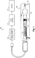
- Fig. 1 is a diagrammatic schematic view of an ultrasound imaging system 100 according to an embodiment of the present disclosure.
- an elongate member 102 such as a catheter, guide wire, or guide catheter
- the distal-most end of the elongate member 102 includes a scanner assembly 106 with an array of ultrasound transducers and associated control circuitry.
- the ultrasound transducers are activated and ultrasonic energy is produced.
- a portion of the ultrasonic energy is reflected by the vessel 104 and the surrounding anatomy and received by the transducers.
- Corresponding echo information is passed along through a Patient Interface Monitor (PIM) 108 to an IVUS console 110, which renders the information as an image for display on a monitor 112.
- PIM Patient Interface Monitor
- the imaging system 100 may use any of a variety of ultrasonic imaging technologies. Accordingly, in some embodiments of the present disclosure, the IVUS imaging system 100 is a solid-state IVUS imaging system incorporating an array of piezoelectric transducers fabricated from lead-zirconate-titanate (PZT) ceramic. In some embodiments, the system 100 incorporates capacitive micromachined ultrasonic transducers (CMUTs), or piezoelectric micromachined ultrasound transducers (PMUTs).
- CMUTs capacitive micromachined ultrasonic transducers
- PMUTs piezoelectric micromachined ultrasound transducers
- the IVUS system 100 includes some features similar to traditional solid-state IVUS system, such as the EagleEye ® catheter available from Volcano Corporation and those disclosed in U.S. Patent No. 7,846,101 .
- the elongate member 102 includes the ultrasound scanner assembly 106 at a distal end of the member 102, which is coupled to the PIM 108 and the IVUS console 110 by a cable 114 extending along the longitudinal body of the member 102.
- the cable 114 caries control signals, echo data, and power between the scanner assembly 106 and the remainder of the IVUS system 100.
- the elongate member 102 further includes a guide wire exit port 116.
- the guide wire exit port 116 allows a guide wire 118 to be inserted towards the distal end in order to direct the member 102 through a vascular structure ( i . e ., a vessel) 104.
- the IVUS device is a rapid-exchange catheter.
- the elongate member 102 also includes an inflatable balloon portion 120 near the distal tip.
- the balloon portion 120 is open to a lumen that travels along the length of the IVUS device and ends in an inflation port (not shown). The balloon 120 may be selectively inflated and deflated via the inflation port.
- the PIM 108 facilitates communication of signals between the IVUS console 110 and the elongate member 102 to control the operation of the scanner assembly 106. This includes generating control signals to configure the scanner, generating signals to trigger the transmitter circuits, and/or forwarding echo signals captured by the scanner assembly 106 to the IVUS console 110. With regard to the echo signals, the PIM 108 forwards the received signals and, in some embodiments, performs preliminary signal processing prior to transmitting the signals to the console 110. In examples of such embodiments, the PIM 108 performs amplification, filtering, and/or aggregating of the data. In an embodiment, the PIM 108 also supplies high- and low-voltage DC power to support operation of the circuitry within the scanner assembly 106.
- the IVUS console 110 receives the echo data from the scanner assembly 106 by way of the PIM 108 and processes the data to create an image of the tissue surrounding the scanner assembly 106.
- the console 110 may also display the image on the monitor 112.
- the ultrasound imaging system 100 may be utilized in a variety of applications and can be used to image vessels and structures within a living body.
- Vessel 104 represents fluid filled or surrounded structures, both natural and man-made, within a living body that may be imaged and can include for example, but without limitation, structures such as: organs including the liver, heart, kidneys, as well as valves within the blood or other systems of the body.
- the images may also include imaging man-made structures such as, but without limitation, heart valves, stents, shunts, filters and other devices positioned within the body.
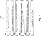
- Fig. 2 is a flow diagram of a method 200 of utilizing the IVUS system 100 according to an example provided for further explanation. It is understood that additional steps can be provided before, during, and after the steps of method 200, and that some of the steps described can be replaced or eliminated for other examples of the method.
- a surgeon places a guide wire 118 in the vessel 104.
- the guide wire 118 is threaded through at least a portion of the distal end of the elongate member 102 either before, during, or after placement of the guide wire 118.
- the elongate member 102 is advanced over the guide wire.
- a guide catheter is advanced in the vessel 104 in block 202 and the elongate member 102 is advanced within the guide catheter in block 204.
- the scanner assembly 106 is activated. Signals sent from the PIM 108 to the scanner assembly 106 via the cable 114 cause transducers within the assembly 106 to emit a specified ultrasonic waveform. The ultrasonic waveform is reflected by the vessel 104. Referring to block 208 of Fig. 2 , the reflections are received by the transducers within the scanner assembly 106 and are amplified for transmission via the cable 114. The echo data is placed on the cable 114 and sent to the PIM 108. The PIM 108 amplifies the echo data and/or performs preliminary pre-processing, in some instances. Referring to block 210 of Fig.
- the PIM 108 retransmits the echo data to the IVUS console 110.
- the IVUS console 110 aggregates and assembles the received echo data to create an image of the vessel 104 for display on the monitor 112.
- the IVUS device is advanced beyond the area of the vessel 104 to be imaged and pulled back as the scanner assembly 106 is operating, thereby exposing and imaging a longitudinal portion of the vessel 104.
- a pullback mechanism is used in some instances.
- a typical withdraw velocity is 0.5 mm/s.
- the member 102 includes an inflatable balloon portion 120.
- the device may be positioned adjacent to a stenosis (narrow segment) or an obstructing plaque within the vessel 104 and inflated in an attempt to widen the restricted area of the vessel 104.
- the system 100 and in particular the elongate member 102, is designed to provide high-resolution imaging from within narrow passageways.
- embodiments of the present disclosure have improved flexibility and reduced diameter allowing greater maneuverability and leading to increased patient safety and comfort.
- the elongate member 102 is generally flexible, it may include components within it that are not.
- the ultrasound scanner assembly 106 is often rigid. As a result, the scanner assembly 106 may limit the agility of the elongate member 102 and may make navigating the vessel 104 more difficult.
- an ultrasound scanner assembly 106 that is smaller longitudinally and circumferentially, as provided herein, may allow for a thinner elongate member 102 with improved agility to navigate complex vessels 104. Specific embodiments also provide faster, less expensive, and more reliable methods of manufacturing the scanner assembly 106.
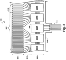
- Fig. 3 is a top view of a portion of an ultrasound scanner assembly 106 according to an example provided for further explanation.
- Fig. 3 depicts the ultrasound scanner assembly 106 in its flat form.
- the assembly 106 includes a transducer array 302 formed in a transducer region 304 and transducer control logic dies 306 (including dies 306A and 306B) formed in a control region 308, with a transition region 310 disposed therebetween.
- the array 302 may include any number and type of ultrasound transducers 312, although for clarity only a limited number of ultrasound transducers are illustrated in Fig. 3 .
- the transducer array 302 includes 64 individual ultrasound transducers 312.
- the transducer array 302 includes 32 ultrasound transducers 312. Other numbers are both contemplated and provided for.
- the ultrasound transducers 312 are piezoelectric micromachined ultrasound transducers (PMUTs) fabricated on a microelectromechanical system (MEMS) substrate using a polymer piezoelectric material, for example as disclosed in U.S. Patent 6,641,540 .
- the transducer array includes piezoelectric transducers fabricated from bulk PZT ceramic or single crystal piezoelectric material, piezoelectric micromachined ultrasound transducers (PMUTs), capacitive micromachined ultrasound transducers (CMUTs), other suitable ultrasound transmitters and receivers, and/or combinations thereof.
- PMUTs piezoelectric micromachined ultrasound transducers
- CMUTs capacitive micromachined ultrasound transducers
- other suitable ultrasound transmitters and receivers and/or combinations thereof.
- the scanner assembly 106 may include various transducer control logic, which in the illustrated exampleis divided into discrete control logic dies 306.
- the control logic of the scanner assembly 106 performs: decoding control signals sent by the PIM 108 across the cable 114, driving one or more transducers 312 to emit an ultrasonic signal, selecting one or more transducers 312 to receive a reflected echo of the ultrasonic signal, amplifying a signal representing the received echo, and/or transmitting the signal to the PIM across the cable 114.
- a scanner assembly 106 having 64 ultrasound transducers 312 divides the control logic across nine control logic dies 306, of which five are shown.
- control logic dies 306 are characterized by the number of transducers they are capable of driving, and exemplary control logic dies 306 drive 4, 8, and 16 transducers.
- the control logic dies are not necessarily homogenous.
- a single controller is designated a master control logic die 306A and contains the communication interface for the cable 114.
- the master control circuit may include control logic that decodes control signals received over the cable 114, transmits control responses over the cable 114, amplifies echo signals, and/or transmits the echo signals over the cable 114.
- the remaining controllers are slave controllers 306B.
- the slave controllers 306B may include control logic that drives a transducer 312 to emit an ultrasonic signal and selects a transducer 312 to receive an echo.
- the master controller 306A does not directly control any transducers 312.
- the master controller 306A drives the same number of transducers 312 as the slave controllers 306B or drives a reduced set of transducers 312 as compared to the slave controllers 306B.
- a single master controller 306A and eight slave controllers 306B are provided with eight transducers assigned to each slave controller 306B.
- the transducer control logic dies 306 and the transducers 312 are mounted on a flex circuit 314 that provides structural support and interconnects for electrical coupling.
- the flex circuit 314 may be constructed to include a film layer of a flexible polyimide material such as KAPTON TM (trademark of DuPont).
- suitable materials include polyester films, polyimide films, polyethylene napthalate films, or polyetherimide films, other flexible printed semiconductor substrates as well as products such as Upilex ® (registered trademark of Ube Industries) and TEFLON ® (registered trademark of E.I. du Pont).
- the film layer is configured to be wrapped around a ferrule to form a cylindrical toroid in some instances.
- the thickness of the film layer is generally related to the degree of curvature in the final assembled scanner assembly 106.
- the film layer is between 5 ⁇ m and 100 ⁇ m, with some particular examples being between 12.7 ⁇ m and 25.1 ⁇ m.
- the flex circuit 314 further includes conductive traces formed on the film layer that carry signals between the control logic dies 306 and the transducers 312 and that provide a set of pads for connecting the conductors of cable 114.
- Suitable materials for the conductive traces include copper, gold, aluminum, silver, nickel, and tin and may be deposited on the flex circuit 314 by processes such as sputtering, plating, and etching.
- the flex circuit 314 includes a chromium adhesion layer or a titanium-tungsten adhesion layer.
- the width and thickness of the conductive traces are selected to provide proper conductivity and resilience when the flex circuit 314 is rolled.
- an exemplary range for the width of a conductive trace is between 10-50 ⁇ m.
- 20 ⁇ m conductive traces are separated by 20 ⁇ m of space.
- the width of a conductive trace may be further determined by the size of a pad of a device or the width of a wire to be coupled to the trace.
- the thickness of the conductive traces may have a range from about 1 ⁇ m to about 10 ⁇ m, with a typical thickness of 5 ⁇ m.
- the scanner assembly 106 is transitioned from a flat configuration to a rolled or more cylindrical configuration.
- techniques are utilized as disclosed in one or more of U.S. Patent No. 6,776,763 , titled “ULTRASONIC TRANSDUCER ARRAY AND METHOD OF MANUFACTURING THE SAME" and U.S. Patent No. 7,226,417 , titled “HIGH RESOLUTION INTRAVASCULAR ULTRASOUND TRANSDUCER ASSEMBLY HAVING A FLEXIBLE SUBSTRATE” .
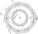
- Fig. 4 is a cross-sectional view of a control region 308 of an ultrasound scanner assembly 106 according to an example provided for further explanation.
- the control region 308 is depicted in its rolled form and contains the transducer control logic dies 306 bonded to the flex circuit 314.
- the flex circuit 314 also includes a conductive ground layer 402.
- the flex circuit includes an outer membrane 404 used to insulate and cover the ground layer 402 and to protect the scanner assembly 106 from the environment. Insulator materials for the outer membrane 404 may be selected for their biocompatibility, durability, hydrophilic or hydrophobic properties, low-friction properties, ultrasonic permeability, and/or other suitable criteria.
- the outer membrane may include Parylene TM (trademark of Union Carbide).
- suitable materials include heat shrink tubing such as polyester or PVDF, a melt-formable layers such as Pebax ® (registered trademark of Arkema) or polyethylene, and/or other suitable membrane materials.
- the flex circuit 314 and the attached elements are rolled around a ferrule 406.
- the lumen region 408 inside the ferrule 406 is open to allow the scanner assembly 106 to be advanced over a guide wire (not shown).
- the ferrule 406 may include a radiopaque material to aid in visualizing the scanner assembly 106 during a procedure.
- encapsulating epoxy 410 fills the spaces between the control logic dies 306 and the ferrule 406.
- control logic dies 306 are coupled to the flex circuit 314 by contact bumps 412.
- the contact bumps 412 may include a metal core, such as a copper core, with a solder portion. During formation, the contact may be heated, causing the solder to flow and join the metal core of the contact bump 412 to the flex circuit 314 trace.
- An underfill material 414 between the control logic dies 306 and the flex circuit 314 may be applied to increase the bond strength, to provide structural support for the control region 308, to insulate conductive structures including the contact bumps 412, and/or to promote thermal conduction.
- control region 308 includes a retaining structure 416 applied over the transducer control logic dies 306.
- the retaining structure 416 may be used during the rolling process, for example, to secure components including the control logic dies 306.
- Encapsulating epoxy 410 fills the space between the transducer control logic dies 306 and the retaining structure 416 and between the retaining structure 416 and the ferrule 406 in some examples.
- the transducer control logic dies 306 at least partially define the shape of the control region 308.
- the portions of the flex circuit 314 adjacent to the control logic dies 306 are relatively flat while the portions of the flex circuit adjacent gaps between the dies 306 are relatively rounded, resulting in a cross-sectional shape that is more polygonal than circular.
- the gaps between control logic dies 306 in the rolled configuration increase the effective diameter 418 of the control region 308.
- half of the circumference of the control region 308 is due to gap space. The result is a larger and more irregular shaped scanner assembly 106.
- control logic dies 306 include interlocking teeth.
- control logic dies 306 may be formed with a recess and projection that interlocks with a recess and projection of an adjacent control logic die 306 to form a box joint or finger joint.
- each of the dies 306 interlocks with two adjacent controllers utilizing a recess and projection interface.
- a control logic die 306 includes a chamfered edge, either alone or in combination with a recess and projection. The chamfered edge may be configured to abut an edge of an adjacent control logic die 306. In some such examples, the edge of the adjacent controller is chamfered as well.
- Edge configurations that interlock adjacent control logic dies 306 may allow for closer control logic die spacing and a reduced diameter 418 in the rolled configuration. Such configurations may also interlock to create a rigid structure and thereby provide additional structural support for the rolled scanner assembly 106. Additionally or in the alternative, narrower and more numerous control logic dies 306 are used in place of larger dies in order to reduce the size of the flat areas of the controller region 308. It follows that designs utilizing 8, 9, 16, or more transducer control logic dies 306 have a more circular cross-section than designs with 4 or 5 controllers.
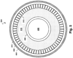
- Fig. 5 is a cross-sectional view of a transducer region 304 of an ultrasound scanner assembly 106 according to an example of the present disclosure.
- the transducer region 304 is depicted in its rolled form.
- the transducer region 304 of the scanner contains the transducers 312, which, as previously disclosed, are physically attached to the flex circuit 314 and are electrically coupled to the traces of the flex circuit 314.
- the size, shape, and spacing of the ultrasound transducers 312 at least partially define the shape of the transducer region 304, with the portions of the flex circuit 314 that are adjacent to the transducers 312 being relatively flat and the portions of the flex circuit that are adjacent gaps between transducers 312 being relatively rounded.
- the transducer region 304 may be more circular than the control region 308. In examples with 64 ultrasound transducers 312, the cross-section of the transducer region 304 is nearly circular.
- the scanner assembly 106 may include a transition region 310 as shown in Fig. 6.
- Fig. 6 is a longitudinal perspective view of a portion of an ultrasound scanner assembly 106 depicted in its rolled form according to an example of the present disclosure.
- the transition region 310 is located between the transducer region 304 and the control region 308.
- the transition region 310 is free of rigid structures. Instead, the cross-sectional shape is defined by the adjacent regions 304 and 308.
- the shape of the transition region 310 transitions between that of the transducer region 304 and the controller region 308.
- the transition region 310 may be used to reduce sharp angles that can stress the flex circuit 314 and/or the conductive traces. Greater differences in cross-sectional shapes may result in a longer transition region 310.
- the transition region 310 is approximately 1 to 1.5 catheter diameters in order to transition from square to substantially round. This works out to be between 1000 and 1500 ⁇ m for a 3Fr catheter.
- the transition region 310 is approximately 0.5 to 0.75 catheter diameters, or between 500 and 750 ⁇ m for a 1 mm outer diameter (3Fr) catheter.
- the scanner assembly 106 (including the transition region 310) is typically inflexible or rigid compared to the surrounding portion of the device, reducing the length of the transition region 310 results in a more agile IVUS device capable of maneuvering through complex vascular branches and producing less discomfort in the patient.
- a technique for reducing the size of the scanner assembly according to the embodiments of the present invention includes manufacturing the transducers and/or the control circuitry on a rollable semiconductor substrate. This reduces the irregularity caused by the flat transducers 312 and control logic dies 306 of the previous examples, and may reduce both the longitudinal length and the diameter of the scanner assembly.
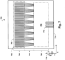
- Fig. 7 is a top view of an ultrasound scanner assembly 700 incorporating a rollable semiconductor substrate according to embodiments of the present invention. Fig. 7 depicts the ultrasound scanner assembly 700 in its flat form. In many respects, the ultrasound scanner assembly 700 may be substantially similar to scanner assembly 106 of Figs. 3-6 and includes a transducer array 702 that includes any number and type of ultrasound transducers 703 formed in a transducer region 704.
- the transducer array 702 includes 64 CMUT transducers 703.
- the ultrasound scanner assembly 700 may also include control logic circuitry 706 formed in a control region 708 with a transition region 710 disposed therebetween.
- the ultrasound scanner assembly 700 may also include contact pads 712 for coupling the scanner assembly 700 to a cable 114 for communication with other components of an IVUS system such as a PIM 108.
- the transducers 312 and control logic dies 306 of Fig. 3 are formed on a rigid substrate
- the transducer array 702 and the control circuitry 706 of embodiments of the present invention are formed on a rollable substrate 714.
- the elements of the scanner assembly 700 are shaped into a curve as indicated by arrow 716 and many of the challenges involved in arranging flat components into a roughly circular profile are avoided.
- the transducer region 704 and the control region 708 have a more circular cross-sectional shape in the rolled configuration, as shown in more detail in the context of Figs. 8 and 9 .
- the overall size of the scanner assembly 700 is reduced.
- the diameter of the scanner assembly (and correspondingly the circumference and gauge) is reduced.
- a shorter transition region 710 may be utilized thereby reducing the longitudinal length of the scanner assembly 700.
- the transition region 710 is not used to transition between the profiles of the control region 708 and the transducer region 704, the shorter transition region 710 may still prove useful as a sacrificial region during dicing.
- control region 708 measures approximately 1.5 mm in the Y direction
- transition region 710 measures approximately 1 mm in the Y direction
- transducer region 704 measures between approximately .75 mm and .5 mm in the Y direction.
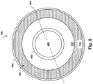
- Fig. 8 is a cross-sectional view of a control region 708 of an ultrasound scanner assembly 700 according to an embodiment of the present invention.
- the control region 708 is illustrated in its rolled form and includes the control circuitry 706 formed on a rollable semiconductor substrate 714.
- the semiconductor substrate 714 is flexed to form a cylinder and more specifically, a cylindrical toroid.
- the resulting cross-sectional profile of the control region 708 is substantially circular without flat regions seen in other examples.
- the control circuitry 706 is packed more densely. Because dies often include reserved areas for separating dies during manufacturing (scribe lines), device density is further improved by using a single rollable substrate 714. Similarly, dies often include insulators, pads, and other bulk that may be eliminated through the use of a rollable substrate 714.
- control circuitry 706 is reduced when compared to embodiments utilizing discrete dies. For example, partitioning the control circuitry 706 across dies often involves duplicating functionality. This duplicate logic may be avoided in embodiments where the control circuitry 706 remains together. As yet another example, partitioning the control circuitry 706 across dies often involves adding large and power hungry I/O circuitry to transmit, synchronize, and amplify signals between dies. This too may be avoided in embodiments where the control circuitry 706 remains together on the semiconductor substrate 714. Furthermore, transmitting analog signals between dies, such as echo data, may introduce noise. For these reasons and others, the control region 708 incorporating a flexible substrate 714 may be smaller and more efficient than other configurations and may provide greater imaging fidelity. In particular, the control region 708 may have a smaller diameter 804 and may have a corresponding outer diameter less than 1 mm (gauge less than 3Fr).
- the devices formed on the substrate 714 i.e ., the transistors of the control circuitry 706) become curved and rearranged in a cylindrical arrangement.
- the devices may be oriented on the substrate 714 in such a manner as to reduce stress and the possibility of cracking when rolled.
- the devices may be aligned such that the gate width direction extends along the longitudinal axis of the substrate 714 in the rolled form.
- the active regions and the gate structures of the control circuitry 706 are arranged on the outer surface of the substrate 714 when in the rolled form, whereas in other embodiments, the active regions and the gate structures are arranged on the inner surface of the substrate when in the rolled form.
- control region 708 includes an outer jacket 802 used to insulate the rollable semiconductor substrate 714 and to protect the scanner assembly 700 from the environment.
- the insulator materials for the outer jacket 802 may be selected for their biocompatibility, durability, hydrophilic or hydrophobic properties, low-friction properties, ultrasonic permeability, and/or other suitable criteria.
- the outer jacket 802 includes KAPTON TM , polyester films, polyimide films, polyethylene napthalate films, and/or Upilex ® .
- the outer jacket 802 includes Parylene TM , heat shrink tubing such as polyester or PVDF, a melt-formable layers such as Pebax ® (registered trademark of Arkema) or polyethylene, and/or other suitable membrane materials.
- the outer jacket 802 includes a flexible circuit, such as a polyimide or liquid crystal polymer-based flexible circuit. The flexible circuit may be further jacketed by a shrink fit or other jacket material.
- suitable shrinkfit materials exist including polyester and/or Pebax ® .
- a layer of the outer jacket 802 is formed with proper thickness and acoustic impedance to act as a matching layer for ultrasound signals.
- the matching layer typically has an acoustic impedance between that of the ultrasound transducer and the surrounding vessel and provides a smoother acoustic transition with reduced reflections.
- control region 708 is formed around a ferrule 406 and includes an encapsulating epoxy 410 filling the space between the semiconductor substrate 714 and the ferrule 406.
- the lumen region 408 inside the ferrule 406 is open to allow the scanner assembly 700 to be advanced over a guide wire (not shown).
- the ferrule 406 may include a radiopaque material to aid in visualizing the scanner assembly 700 during a procedure.
- Fig. 9 is a cross-sectional view of a transducer region 704 of an ultrasound scanner assembly 700 according to an embodiment of the present invention.
- the transducer region 704 is depicted in its rolled form and includes a transducer array 702 formed on a rollable semiconductor substrate 714.
- the transducer array 702 includes any number any number and type of ultrasound transducers 703, and in an exemplary embodiment includes 64 CMUT transducers.
- the semiconductor substrate 714 is flexed to form a cylinder or cylindrical toroid and the resulting cross-sectional profile of the transducer region 704 is substantially circular.
- the transducers of the transducer array 702 become curved and take on a cylindrical arrangement.
- the transducers of the transducer array 702 are arranged on the outer surface of the substrate 714 when in the rolled form.
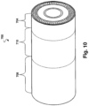
- Fig. 10 is a longitudinal perspective view of a portion of an ultrasound scanner assembly 700 depicted in its rolled form according to an embodiment of the present invention.
- the scanner assembly 700 includes a transition region 710 located between the transducer region 704 and the control region 708.
- the cross-sectional profiles of the transducer region 704 and the control region 708 are similar and thus the transition region 710 may be shorter in the longitudinal direction as compared to the previous examples.
- the gauge or thickness of the rolled scanner assembly 700 may be less than that of other configurations.
- the outer diameter of the scanner assembly 700 is between 0.67 - 1 mm (2-3Fr) and, in a specific embodiment, the outer diameter of the scanner assembly 700 measures approximately 0.67 mm (2Fr).
- FIG. 11 is a flow diagram of the method 1100 of manufacturing the ultrasound scanner assembly 700 according to an embodiment of the present invention. It is understood that additional steps can be provided before, during, and after the steps of method 1100 and that some of the steps described can be replaced or eliminated for other embodiments of the method.
- Figs. 12-16 are cross-sectional views of a scanner assembly 700 being manufactured by the method according to an embodiment of the present invention. Figs. 12-16 each show transducer control circuitry 706 being manufactured in a control region 708 and a transducer array 702 being manufactured in a transducer region 704.
- Fig. 17 is a top view of a scanner assembly 700 formed on a wafer undergoing the method of manufacturing according to an embodiment of the present invention.
- Substrate 714 may be any base material on which processing is conducted to produce layers of materials, pattern features, and/or integrated circuits such as those used to manufacture transducer control circuitry 706.
- semiconductor substrates include a bulk silicon substrate, an elementary semiconductor substrate such as a silicon or germanium substrate, a compound semiconductor substrate such as a silicon germanium substrate, an alloy semiconductor substrate, and substrates including non-semiconductor materials such as glass and quartz.
- transistors of the control circuitry 706 are formed on the substrate 714 in the control region 708.
- An exemplary process for forming the transistors includes growing a pad oxide layer over the substrate, depositing a nitride layer by chemical vapor deposition, performing a reactive ion etching to form a trench, growing a shallow trench isolation feature oxide, chemical-mechanical planarization, channel implantation, formation of a gate oxide, polysilicon deposition, etching to form a gate structure, source-drain implantation, forming of sidewall spacers, performing a self-aligned silicide process, forming one or more interconnect layers, forming a pad layer, and/or other fabrication processes known to one of skill in the art.
- the process for forming the control circuitry 706 produces gate structures 1202, shallow trench isolation features 1204, conductive interconnects 1206, and insulator layers 1208.
- CMUT transducers are formed in block 1106 by depositing a dielectric layer 1302 on the substrate 714 and depositing a sacrificial layer 1304, such as a polysilicon layer, on the dielectric layer 1302 to define the CMUT vacuum gap, which acts as a resonance chamber.
- a sacrificial layer 1304 such as a polysilicon layer
- further dielectric material 1402 is deposited over the sacrificial layer 1304 with holes formed therein to allow the sacrificial layer 1304 to be etched.
- the sacrificial layer 1304 is etched away from underneath the dielectric and the holes are filled with additional dielectric material 1402. This may be performed in a vacuum so that the remaining cavity is a vacuum gap 1502 within the dielectric formation of 1302 and 1402.
- the material over the vacuum gap 1502 is referred to as a diaphragm 1504 or drumhead and is free to deflect into the vacuum gap 1502.
- An electrode 1506 is formed over the vacuum gap that together with a conductive region of the substrate 714 form a parallel plate capacitor. Deflection of the diaphragm 1504 and the electrode 1506 into the vacuum gap, such as deflection caused by an ultrasonic wave, changes the electrical behavior of the capacitor. These changes can be measured in order to determine properties of the wave that caused them.
- One or more interconnect layers 1206 and/or passivation layers 1208 may then be formed over the electrode 1506.
- a polymer coating such as the outer jacket 802 described in Fig. 8 may be formed on the substrate 714 and insulates the control circuitry 706 and the transducer array 702. Additionally or in the alternative, the outer jacket 802 may be formed over the substrate 714 after the rolling of the substrate 714 during the final assembly in block 1116, described below.
- the substrate 714 is made rollable.
- the substrate 714 in its initial form may be rigid for easier manufacturing of the transducer array 702 and the control circuitry 706.
- the substrate 714 is made rollable by performing a thinning process. Thinning the substrate 714 to a thickness of approximately 10 ⁇ m or less results in a substrate 714 that is flexible enough to be rolled. Suitable thinning processes include mechanical grinding, wet or dry etching, chemical-mechanical polishing, fracturing, and/or otherwise thinning the substrate 714.
- the wafer thinning process includes mechanical grinding of the substrate 714.
- Mechanical grinding uses abrasive force to remove substrate material.
- the wafer thinning process includes chemical-mechanical polishing (CMP).
- CMP chemical-mechanical polishing
- a polishing pad is installed on a rotating platen.
- a slurry of reactive compounds such as NH4OH and/or abrasive particles such as silica (SiO2), alumina (Al2O3), and ceria (CeO2) is dispensed on the polishing pad.
- the substrate 714, secured in a CMP chuck is forced against the polishing pad as both the platen and the CMP chuck rotate.
- the reactants in the slurry loosen atomic bonds within the surface of the substrate 714, while the mechanical abrasion removes the loosened material.
- CMP is typically slower than purely mechanical grinding but produces less damage to the substrate 714.
- the substrate 714 includes one or more buried layers to control the thinning of the substrate 714.
- the substrate 714 includes a dielectric layer that acts as a stop layer during a mechanical grinding process.
- the substrate 714 includes a buried dielectric layer (e.g., a buried oxide layer) that acts as an etch stop layer during a chemical etching process.
- the substrate 714 includes a cleavage layer that separates from the remainder of the substrate 714 during a mechanical separation process.
- the transducer array 702 and the control circuitry 706 of the scanner assembly 700 are singulated from a wafer 1702.
- several scanner assemblies 700 can be formed on a single wafer 1702.
- approximately two thousand scanner assemblies 700 each measuring 10 mm 2 may be formed on a single 203.2 mm (8") wafer 1702.
- the scanner assemblies 700 are separated using techniques that may include saw dicing, mechanical cutting, laser cutting, physical force, and/or other suitable singulation techniques.
- the scanner assembly 700 is rolled to have a substantially cylindrical form as shown in Figs. 8-10 . Because the rolling process curves the transistors of the control circuitry 706 and the transducers 703 of the transducer array 702, flat areas and other irregularities are reduced. In some embodiments, rolling includes applying a retaining structure 416 before the scanner assembly 700 is shaped into the substantially cylindrical form.
- the scanner assembly 700 is provided to a finishing facility for final assembly, which may include applying an encapsulating epoxy 410, attaching the cable 114, and/or sealing the scanner assembly 700.
- a finishing facility for final assembly which may include applying an encapsulating epoxy 410, attaching the cable 114, and/or sealing the scanner assembly 700.
- the scanner assembly 700 may incorporate any suitable ultrasound transducer technology, including the CMUT transducer 703 illustrated in Fig. 16 .
- Suitable transducers 703 are illustrated in further detail in Figs. 18A, 18B , 19, and 20 .
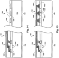
- Figs. 18A and 18B are top views of a portion of a transducer array 702 according to an embodiment of the present disclosure.
- Fig. 18B is an enlarged view of the portion.
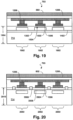
- Fig. 19 is a cross-sectional view of a portion of a transducer 703 incorporating an array of CMUT elements 1902 according to an embodiment of the present disclosure.
- Fig. 20 is a cross-sectional view of a portion of a transducer 703 incorporating an array of piezoelectric elements 2002 according to an embodiment of the present disclosure.
- each transducer 703 of the transducer array 702 includes an array of transducer elements 1802.
- Each element 1802 is itself a transducer operable to generate a waveform by vibrating a diaphragm 1504 (i.e ., a drumhead) and to produce an electrical signal in response to a received waveform.
- each element 1802 may include a diaphragm 1504, a chamber such as a vacuum gap 1502, an associated electrode 1506, and/or any other ancillary structure. Because of the limited displacement of each element 1802, each transducer 703 may include multiple elements 1802 electrically connected in parallel to increase the effective surface area.
- each diaphragm 1504 is substantially circular with a diameter of approximately 10 ⁇ m, although it is understood in further embodiments the transducers 703 include other sizes and shapes of diaphragm 1504.
- the number of elements 1802 has been reduced, and while each transducer 703 may include any number of elements 1802, in an exemplary embodiment, each transducer 703 includes approximately 100 elements.
- an array of elements 1802 can be tuned to more than one frequency by adjusting the number of elements 1802 operating in unison.
- An array can also produce specialized waveforms by adjusting the firing sequence of the elements 1802.
- elements 1802 of a transducer 703 are arranged into groups (indicated by dashed boxes 1804). While the elements 1802 of each group are electrically connected in parallel and thus operate in unison, the groups can be independently controlled or addressed to produce a number of different ultrasonic waveforms at a number of different characteristic frequencies.
- a single transducer 703 can support multiple imaging modes, with common modes including both 20 MHz and 40 MHz modes.
- the transducer 702 includes CMUT transducer elements 1902.
- the three illustrated elements each include a vacuum gap 1502 defined by a dielectric layer 1302 formed on the substrate 714, a diaphragm 1504 formed over the vacuum gap 1502, an electrode 1506 formed over the diaphragm, and an interconnect 1206 electrically coupling the diaphragms 1504 to other diaphragms 1504 and to the control circuitry (not shown).
- the CMUT transducer elements 1902 are well suited for the rollable substrate 714 because their overall profile can be quite thin.
- the combined thickness 1904 of the diaphragm 1504, the vacuum gap 1502, and the substrate 714 is less than or substantially equal to 10 ⁇ m.
- the diaphragm 1504 has a thickness of approximately 1 ⁇ m
- the vacuum gap 1502 has a thickness of approximately .1 ⁇ m.
- a portion of another transducer 702 that includes piezoelectric transducer elements 2002 is shown.
- the piezoelectric elements 2002 are a suitable substitute for the CMUT elements 1902 described above and, when arranged in an array to form a transducer 703 may have a top view substantially similar to that of Figs. 18A and 18B .
- the piezoelectric elements 2002 each include a chamber 2004 formed in the substrate 714.
- a piezoelectric thin-film 2006 is formed over the chamber 2004.
- the piezoelectric elements 2002 can be quite thin.
- the combined thickness 2008 of the piezoelectric thin-film 2006 and the substrate 714 containing the chamber 2004 have a combined thickness between approximately 5 ⁇ m and approximately 10 ⁇ m, with the piezoelectric thin-film 2006 having a thickness between approximately 1 ⁇ m and approximately 2 ⁇ m.
- Figs. 19 and 20 provide an effective element size that is much greater than the individual diaphragm size. This allows the transducer to provide a more powerful ultrasonic signal while transmitting and to produce a stronger electrical signal while receiving.
- the operational frequency of a transducer can be tuned by adjusting the number of elements operating in parallel. The result is a more sensitive transducer in a smaller package.
- the present disclosure provides an improved IVUS device with a scanner assembly that is designed to be both smaller and more uniform, and provides a method for manufacturing the scanner assembly improves yield and takes much of the complexity out of the manufacturing.
Description
- The present disclosure relates generally to intravascular ultrasound (IVUS) imaging and, in particular, to a solid-state IVUS imaging system. In various embodiments, the IVUS imaging system includes an array of ultrasound transducers, such as piezoelectric zirconate transducers (PZTs), capacitive micromachined ultrasonic transducers (CMUTs), and/or piezoelectric micromachined ultrasound transducers (PMUTs), formed on a semiconductor substrate along with associated control logic. The semiconductor substrate is then rolled into a cylindrical form to form a scanner assembly and disposed at a distal end of an intravascular elongate member. The resulting device is suitable for advancing into an enclosed space and imaging the surrounding structures. Some examples provide an IVUS imaging system particularly suited to imaging a human blood vessel.
- Intravascular ultrasound (IVUS) imaging is widely used in interventional cardiology as a diagnostic tool for assessing a diseased vessel, such as an artery, within the human body to determine the need for treatment, to guide the intervention, and/or to assess its effectiveness. An IVUS device includes one or more ultrasound transducers arranged at a distal end of an elongate member. The elongate member is passed into the vessel thereby guiding the transducers to the area to be imaged. The transducers emit ultrasonic energy in order to create an image of the vessel of interest. Ultrasonic waves are partially reflected by discontinuities arising from tissue structures (such as the various layers of the vessel wall), red blood cells, and other features of interest. Echoes from the reflected waves are received by the transducer and passed along to an IVUS imaging system. The imaging system processes the received ultrasound echoes to produce a cross-sectional image of the vessel where the device is placed.
- There are two general types of IVUS devices in use today: rotational and solid-state (also known as synthetic aperture phased array). For a typical rotational IVUS device, a single ultrasound transducer element is located at the tip of a flexible driveshaft that spins inside a plastic sheath inserted into the vessel of interest. The transducer element is oriented such that the ultrasound beam propagates generally perpendicular to the axis of the device. The fluid-filled sheath protects the vessel tissue from the spinning transducer and driveshaft while permitting ultrasound signals to propagate from the transducer into the tissue and back. As the driveshaft rotates, the transducer is periodically excited with a high voltage pulse to emit a short burst of ultrasound. The same transducer then listens for the returning echoes reflected from various tissue structures. The IVUS imaging system assembles a two dimensional display of the vessel cross-section from a sequence of pulse/acquisition cycles occurring during a single revolution of the transducer.
- In contrast, solid-state IVUS devices utilize a scanner assembly that includes an array of ultrasound transducers distributed around the circumference of the device connected to a set of transducer controllers. The transducer controllers select transducer sets for transmitting an ultrasound pulse and for receiving the echo signal. By stepping through a sequence of transmit-receive sets, the solid-state IVUS system can synthesize the effect of a mechanically scanned transducer element but without moving parts. Since there is no rotating mechanical element, the transducer array can be placed in direct contact with the blood and vessel tissue with minimal risk of vessel trauma. Furthermore, because there is no rotating element, the interface is simplified. The solid-state scanner can be wired directly to the imaging system with a simple electrical cable and a standard detachable electrical connector.
- Because an IVUS device is advanced into a confined space, device agility, which strikes a balance between flexibility and controllability, is an important characteristic. Rotational devices tend to smoothly advance around corners due to the flexible rotating drive shaft contained within the sheath. However, rotational IVUS devices often require a long rapid exchange tip to engage the guidewire, and the long tip may limit the advance of the imaging core containing the transducer. For example, this may prevent the device from being advanced to very distal locations within the coronary arteries. On the other hand, solid-state IVUS devices may have a shorter tip as the guidewire can pass through the interior lumen of the scanner. However, some solid-state designs have rigid segments that limit the ability to advance the elongate member around sharp bends in the vasculature. Solid-state IVUS devices also tend to be larger in diameter than rotational devices to accommodate the transducer array and the associated electronics.
- While existing IVUS imaging systems have proved useful, there remains a need for improvements in the design of the solid-state scanner to reduce its overall diameter and to reduce the length of rigid portions of the elongate member in order to provide improved access to the vasculature. In addition, the improvements to fabrication and assembly techniques would also prove beneficial because of the difficulties inherent in assembling miniscule components. Accordingly, the need exists for improvements to the scanner assembly and its components, and to the methods used in manufacturing these elements.
-
US 2010/262014 A1 , according to its abstract, describes ultrasonic scanners and methods of manufacturing ultrasonic scanners. One embodiment of a method includes integrating a flexible electronic device (e.g. an IC) and a flexible ultrasonic transducer (e.g. a portion of a circular CMUT array) with a flexible member. The IC, the transducer, and the flexible member can form a flexible subassembly which is rolled up to form an ultrasonic scanner. The integration of the IC and the transducer can occur at the same time. In the alternative, the integration of the electronic device can occur before the integration of the transducer. Moreover, the integration of the transducer can include using a semiconductor technique. Furthermore, the rolled up subassembly can form a lumen or can be attached to a lumen. The method can include folding a portion of the flexible subassembly to form a forward looking transducer. The flexible member of some subassemblies can include a pair of arms. -
US 7 846 101 B2 , according to its abstract, describes an ultrasound transducer assembly of that includes a flexible circuit to which an ultrasound transducer array and integrated circuitry are attached during fabrication of the ultrasound transducer assembly. The flexible circuit comprises a flexible substrate to which the integrated circuitry and transducer elements are attached while the flexible substrate is in a substantially flat shape. The flexible circuit further comprises electrically conductive lines that are deposited upon the flexible substrate. The electrically conductive lines transport electrical signals between the integrated circuitry and the transducer elements. After assembly, the flexible circuit is re-shapeable into a final form such as, for example, a substantially cylindrical shape. -
US 2010/280388 A1 , according to its abstract, describes ultrasonic scanners and methods of manufacturing ultrasonic scanners. One embodiment of a method includes integrating a flexible electronic device (e.g. an IC) and a flexible ultrasonic transducer (e.g. a portion of a circular CMUT array) with a flexible member. The IC, the transducer, and the flexible member can form a flexible subassembly which is rolled up to form an ultrasonic scanner. The integration of the IC and the transducer can occur at the same time. In the alternative, the integration of the electronic device can occur before the integration of the transducer. Moreover, the integration of the transducer can include using a semiconductor technique. Furthermore, the rolled up subassembly can form a lumen or can be attached to a lumen. The method can include folding a portion of the flexible subassembly to form a forward looking transducer. The flexible member of some subassemblies can include a pair of arms. - In Don lsarakorn: "Epitaxial Piezoelectric MEMS on Silicon", Ecole Polytechnique Federale de Lausanne, 2011, according to its abstract, several aspects related to the development of epitaxial piezoelectric MEMS on silicon are investigated, which cover the following topics: the deposition and integration of high quality epitaxial PZT thin films on silicon wafers; the establishment of microfabrication techniques with associated process flows; and the FEM supported design, and characterization of epitaxial piezoelectric MEMS.
-
US 2007/264732 A1 , according to its abstract, describes medical imaging devices that may comprise an array of ultrasonic transducer elements. Each transducer element may comprise a substrate having a doped surface creating a highly conducting surface layer, a layer of thermal oxide on the substrate, a layer of silicon nitride on the layer of thermal oxide, a layer of silicon dioxide on the layer of silicon nitride, and a layer of conducting thin film on the layer of silicon dioxide. The layers of silicon dioxide and thermal oxide may sandwich the layer of silicon nitride, and the layer of conducting thin film may be separated from the layer of silicon nitride by the layer of silicon dioxide. - Xuefend Zhuang et al. "Fabrication of Flexible Transducer Arrays With Through-Wafer Electrical Interconnects Based on Trench Refilling With PDMS", Journal of Microelectromechanical Systems, 2008, according to its abstract, presents a technique for constructing flexible capacitive micromachined ultrasonic transducer (CMUT) arrays by forming polymer-filled deep trenches in a silicon substrate.
- K. Wong et al. "Curved micromachined ultrasonic transducers", 2003 IEEE Ultrasonics Symposium Proceedings, according to its abstract, outlines the modeling and CMUT design strategies, describes relevant process steps, and details the manufacturing challenges associated with the curving and packaging of a VMUT.
- The object of the present invention is solved by the subject-matter of the independent claims; further embodiments are incorporated in the dependent claims.
- Embodiments of the present disclosure provide a compact and efficient scanner assembly in a solid-state imaging system.
- An intravascular ultrasound (IVUS) device is provided according to
claim 1. - A method of manufacturing an intravascular ultrasound imaging device is provided according to claim 10.
- The present invention utilizes improved fabrication techniques to reduce the diameter and length of the scanner assembly. As the scanner assembly is rigid, decreasing the size creates a more responsive device and may allow for a thinner elongate member. The dimensions of a conventional scanner assembly may be determined in part by the geometric challenges of arranging flat elements such as controllers and transducers into a roughly cylindrical device as well as the need for a transition zone to accommodate differences in the cross-sectional shape along the length of the cylinder. In contrast, in the present invention, the transducers and control logic are formed on a rollable substrate. During the rolling stage, the entire substrate including the transducers and the control logic are curved to form a more cylindrical device. By utilizing space more efficiently, the rollable substrate increases the device density and decreases the size of the scanner assembly. By forming a more uniform profile, the rollable substrate permits a shorter transition zone, further decreasing the length of the scanner assembly along the longitudinal axis of the rolled assembly. The resulting IVUS device is narrower and more flexible and, therefore, able to maneuver through complicated vascular branches.
- The embodiments leverage the advantages of manufacturing the elements of the scanner assembly on a single semiconductor substrate to further reduce device size. Instead of dividing the elements into discrete dies, separating the dies, and reassembling them on a flexible interconnect, in the embodiments of the present invention, the elements remain together on the semiconductor substrate throughout the manufacture of the scanner assembly. This eliminates the packaging bulk associated with multiple dies and results in more reliable interconnections. Furthermore, the yield loss associated with dicing tiny components and bonding them to a flexible interconnect is avoided. As a result, the manufacturing technique simplifies assembly, reduces assembly time, and improves both yield and device reliability.
- Additional embodiments incorporate transducers that are specially adapted to a flexible substrate. The transducers are formed from an array of diaphragms or drumheads. As some flexible substrates are relatively thin, the resonance chamber of each diaphragm may be shallow. However, by connecting several diaphragms in parallel, the effective size is much larger. This allows the transducer to provide a more powerful ultrasonic signal while transmitting and to produce a stronger electrical signal while receiving. In addition, the operational frequency of a transducer can be tuned by adjusting the number of diaphragms operating in parallel. The result is a more sensitive transducer in a smaller package.
- Additional aspects, features, and advantages of the present disclosure will become apparent from the following detailed description.
- Illustrative embodiments of the present disclosure will be described with reference to the accompanying drawings, of which:
-
Fig. 1 is a diagrammatic schematic view of an intravascular ultrasound (IVUS) imaging system according to an embodiment of the present disclosure. -
Fig. 2 is a flow diagram of a method of utilizing the IVUS system according to an example provided for further explanation. -
Fig. 3 is a top view of a portion of an ultrasound scanner assembly according to an example provided for further explanation. -
Fig. 4 is a cross-sectional view of a control region of an ultrasound scanner assembly according to an example provided for further explanation. -
Fig. 5 is a cross-sectional view of a transducer region of an ultrasound scanner assembly according to an example provided for further explanation. -
Fig. 6 is a longitudinal perspective view of a portion of an ultrasound scanner assembly depicted in its rolled form according to an example provided for further explanation. -
Fig. 7 is a top view of an ultrasound scanner assembly incorporating a rollable semiconductor substrate according to an embodiment of the present disclosure. -
Fig. 8 is a cross-sectional view of a control region of an ultrasound scanner assembly according to an embodiment of the present disclosure. -
Fig. 9 is a cross-sectional view of a transducer region of an ultrasound scanner assembly according to an embodiment of the present disclosure. -
Fig. 10 is a longitudinal perspective view of a portion of an ultrasound scanner assembly depicted in its rolled form according to an embodiment of the present disclosure. -
Fig. 11 is a flow diagram of the method of manufacturing an ultrasound scanner assembly according to an embodiment of the present disclosure. -
Figs. 12-16 are cross-sectional views of a scanner assembly being manufactured by the method according to an embodiment of the present disclosure. -
Fig. 17 is a top view of a scanner assembly formed on a wafer undergoing the method of manufacturing according to an embodiment of the present disclosure. -
Figs. 18A and 18B are top views of a portion of a transducer array according to an embodiment of the present disclosure. -
Fig. 19 is a cross-sectional view of a portion of a transducer incorporating an array of CMUT elements according to an embodiment of the present disclosure. -
Fig. 20 is a cross-sectional view of a portion of a transducer incorporating an array of piezoelectric elements according to an embodiment of the present disclosure. - For the purposes of promoting an understanding of the principles of the present invention, reference will now be made to the embodiments and examples illustrated in the drawings, and specific language will be used to describe the same. For example, while the IVUS system is described in terms of cardiovascular imaging, it is understood that it is not intended to be limited to this application. The system is equally well suited to any application requiring imaging within a confined cavity. In particular, it is fully contemplated that the features, components, and/or steps described with respect to one embodiment may be combined with the features, components, and/or steps described with respect to other embodiments of the present invention, according to the appended claims. For the sake of brevity, however, the numerous iterations of these combinations will not be described separately.
-
Fig. 1 is a diagrammatic schematic view of anultrasound imaging system 100 according to an embodiment of the present disclosure. At a high level, an elongate member 102 (such as a catheter, guide wire, or guide catheter) of theimaging system 100 is advanced into avessel 104. The distal-most end of theelongate member 102 includes ascanner assembly 106 with an array of ultrasound transducers and associated control circuitry. When thescanner assembly 106 is positioned near the area to be imaged, the ultrasound transducers are activated and ultrasonic energy is produced. A portion of the ultrasonic energy is reflected by thevessel 104 and the surrounding anatomy and received by the transducers. Corresponding echo information is passed along through a Patient Interface Monitor (PIM) 108 to anIVUS console 110, which renders the information as an image for display on amonitor 112. - The
imaging system 100 may use any of a variety of ultrasonic imaging technologies. Accordingly, in some embodiments of the present disclosure, theIVUS imaging system 100 is a solid-state IVUS imaging system incorporating an array of piezoelectric transducers fabricated from lead-zirconate-titanate (PZT) ceramic. In some embodiments, thesystem 100 incorporates capacitive micromachined ultrasonic transducers (CMUTs), or piezoelectric micromachined ultrasound transducers (PMUTs). - In some embodiments, the
IVUS system 100 includes some features similar to traditional solid-state IVUS system, such as the EagleEye® catheter available from Volcano Corporation and those disclosed inU.S. Patent No. 7,846,101 . For example, theelongate member 102 includes theultrasound scanner assembly 106 at a distal end of themember 102, which is coupled to thePIM 108 and theIVUS console 110 by acable 114 extending along the longitudinal body of themember 102. Thecable 114 caries control signals, echo data, and power between thescanner assembly 106 and the remainder of theIVUS system 100. - In an embodiment, the
elongate member 102 further includes a guidewire exit port 116. The guidewire exit port 116 allows aguide wire 118 to be inserted towards the distal end in order to direct themember 102 through a vascular structure (i.e., a vessel) 104. Accordingly, in some instances the IVUS device is a rapid-exchange catheter. In an embodiment, theelongate member 102 also includes aninflatable balloon portion 120 near the distal tip. Theballoon portion 120 is open to a lumen that travels along the length of the IVUS device and ends in an inflation port (not shown). Theballoon 120 may be selectively inflated and deflated via the inflation port. - The
PIM 108 facilitates communication of signals between theIVUS console 110 and theelongate member 102 to control the operation of thescanner assembly 106. This includes generating control signals to configure the scanner, generating signals to trigger the transmitter circuits, and/or forwarding echo signals captured by thescanner assembly 106 to theIVUS console 110. With regard to the echo signals, thePIM 108 forwards the received signals and, in some embodiments, performs preliminary signal processing prior to transmitting the signals to theconsole 110. In examples of such embodiments, thePIM 108 performs amplification, filtering, and/or aggregating of the data. In an embodiment, thePIM 108 also supplies high- and low-voltage DC power to support operation of the circuitry within thescanner assembly 106. - The
IVUS console 110 receives the echo data from thescanner assembly 106 by way of thePIM 108 and processes the data to create an image of the tissue surrounding thescanner assembly 106. Theconsole 110 may also display the image on themonitor 112. Theultrasound imaging system 100 may be utilized in a variety of applications and can be used to image vessels and structures within a living body.Vessel 104 represents fluid filled or surrounded structures, both natural and man-made, within a living body that may be imaged and can include for example, but without limitation, structures such as: organs including the liver, heart, kidneys, as well as valves within the blood or other systems of the body. In addition to imaging natural structures, the images may also include imaging man-made structures such as, but without limitation, heart valves, stents, shunts, filters and other devices positioned within the body. -
Fig. 2 is a flow diagram of amethod 200 of utilizing theIVUS system 100 according to an example provided for further explanation. It is understood that additional steps can be provided before, during, and after the steps ofmethod 200, and that some of the steps described can be replaced or eliminated for other examples of the method. - Referring
block 202 ofFig. 2 and referring still toFig. 1 , in an illustrative example of a typical environment and application of the system, a surgeon places aguide wire 118 in thevessel 104. Theguide wire 118 is threaded through at least a portion of the distal end of theelongate member 102 either before, during, or after placement of theguide wire 118. Referring to block 204 ofFig. 2 , once theguide wire 118 is in place, theelongate member 102 is advanced over the guide wire. Additionally or in the alternative, a guide catheter is advanced in thevessel 104 inblock 202 and theelongate member 102 is advanced within the guide catheter inblock 204. Referring to block 206, once positioned, thescanner assembly 106 is activated. Signals sent from thePIM 108 to thescanner assembly 106 via thecable 114 cause transducers within theassembly 106 to emit a specified ultrasonic waveform. The ultrasonic waveform is reflected by thevessel 104. Referring to block 208 ofFig. 2 , the reflections are received by the transducers within thescanner assembly 106 and are amplified for transmission via thecable 114. The echo data is placed on thecable 114 and sent to thePIM 108. ThePIM 108 amplifies the echo data and/or performs preliminary pre-processing, in some instances. Referring to block 210 ofFig. 2 , thePIM 108 retransmits the echo data to theIVUS console 110. Referring to block 212 ofFig. 2 , theIVUS console 110 aggregates and assembles the received echo data to create an image of thevessel 104 for display on themonitor 112. In some exemplary applications, the IVUS device is advanced beyond the area of thevessel 104 to be imaged and pulled back as thescanner assembly 106 is operating, thereby exposing and imaging a longitudinal portion of thevessel 104. To ensure a constant velocity, a pullback mechanism is used in some instances. A typical withdraw velocity is 0.5 mm/s. In some examples, themember 102 includes aninflatable balloon portion 120. As part of a treatment procedure, the device may be positioned adjacent to a stenosis (narrow segment) or an obstructing plaque within thevessel 104 and inflated in an attempt to widen the restricted area of thevessel 104. - The
system 100, and in particular theelongate member 102, is designed to provide high-resolution imaging from within narrow passageways. To advance the performance of IVUS imaging devices compared to the current state of the art, embodiments of the present disclosure have improved flexibility and reduced diameter allowing greater maneuverability and leading to increased patient safety and comfort. While theelongate member 102 is generally flexible, it may include components within it that are not. For example, theultrasound scanner assembly 106 is often rigid. As a result, thescanner assembly 106 may limit the agility of theelongate member 102 and may make navigating thevessel 104 more difficult. In addition, the bulk of the ultrasound transducers and the associated circuitry in thescanner assembly 106 may make it a limiting factor in the drive towards a smaller-gaugeelongate member 102. For these reasons and others, anultrasound scanner assembly 106 that is smaller longitudinally and circumferentially, as provided herein, may allow for a thinnerelongate member 102 with improved agility to navigatecomplex vessels 104. Specific embodiments also provide faster, less expensive, and more reliable methods of manufacturing thescanner assembly 106. -
Fig. 3 is a top view of a portion of anultrasound scanner assembly 106 according to an example provided for further explanation.Fig. 3 depicts theultrasound scanner assembly 106 in its flat form. Theassembly 106 includes atransducer array 302 formed in atransducer region 304 and transducer control logic dies 306 (including dies 306A and 306B) formed in acontrol region 308, with atransition region 310 disposed therebetween. With respect to thetransducer array 302, thearray 302 may include any number and type ofultrasound transducers 312, although for clarity only a limited number of ultrasound transducers are illustrated inFig. 3 . In an example, thetransducer array 302 includes 64individual ultrasound transducers 312. In a further example, thetransducer array 302 includes 32ultrasound transducers 312. Other numbers are both contemplated and provided for. With respect to the types of transducers, in an example, theultrasound transducers 312 are piezoelectric micromachined ultrasound transducers (PMUTs) fabricated on a microelectromechanical system (MEMS) substrate using a polymer piezoelectric material, for example as disclosed inU.S. Patent 6,641,540 . In alternate examples, the transducer array includes piezoelectric transducers fabricated from bulk PZT ceramic or single crystal piezoelectric material, piezoelectric micromachined ultrasound transducers (PMUTs), capacitive micromachined ultrasound transducers (CMUTs), other suitable ultrasound transmitters and receivers, and/or combinations thereof. - The
scanner assembly 106 may include various transducer control logic, which in the illustrated exampleis divided into discrete control logic dies 306. In various examples, the control logic of thescanner assembly 106 performs: decoding control signals sent by thePIM 108 across thecable 114, driving one ormore transducers 312 to emit an ultrasonic signal, selecting one ormore transducers 312 to receive a reflected echo of the ultrasonic signal, amplifying a signal representing the received echo, and/or transmitting the signal to the PIM across thecable 114. In the illustrated example, ascanner assembly 106 having 64ultrasound transducers 312 divides the control logic across nine control logic dies 306, of which five are shown. Designs incorporating other numbers of control logic dies 306 including 8, 9, 16, 17 and more are utilized in other example. In general, the control logic dies 306 are characterized by the number of transducers they are capable of driving, and exemplary control logic dies 306 drive 4, 8, and 16 transducers. - The control logic dies are not necessarily homogenous. In some examples, a single controller is designated a master control logic die 306A and contains the communication interface for the
cable 114. Accordingly, the master control circuit may include control logic that decodes control signals received over thecable 114, transmits control responses over thecable 114, amplifies echo signals, and/or transmits the echo signals over thecable 114. The remaining controllers areslave controllers 306B. Theslave controllers 306B may include control logic that drives atransducer 312 to emit an ultrasonic signal and selects atransducer 312 to receive an echo. In the depicted example, themaster controller 306A does not directly control anytransducers 312. In other examples, themaster controller 306A drives the same number oftransducers 312 as theslave controllers 306B or drives a reduced set oftransducers 312 as compared to theslave controllers 306B. In an exemplary example, asingle master controller 306A and eightslave controllers 306B are provided with eight transducers assigned to eachslave controller 306B. - The transducer control logic dies 306 and the
transducers 312 are mounted on aflex circuit 314 that provides structural support and interconnects for electrical coupling. Theflex circuit 314 may be constructed to include a film layer of a flexible polyimide material such as KAPTON™ (trademark of DuPont). Other suitable materials include polyester films, polyimide films, polyethylene napthalate films, or polyetherimide films, other flexible printed semiconductor substrates as well as products such as Upilex® (registered trademark of Ube Industries) and TEFLON® (registered trademark of E.I. du Pont). The film layer is configured to be wrapped around a ferrule to form a cylindrical toroid in some instances. Therefore, the thickness of the film layer is generally related to the degree of curvature in the final assembledscanner assembly 106. In some examples, the film layer is between 5 µm and 100 µm, with some particular examples being between 12.7 µm and 25.1 µm. - To electrically interconnect the control logic dies 306 and the transducers, in an example, the
flex circuit 314 further includes conductive traces formed on the film layer that carry signals between the control logic dies 306 and thetransducers 312 and that provide a set of pads for connecting the conductors ofcable 114. Suitable materials for the conductive traces include copper, gold, aluminum, silver, nickel, and tin and may be deposited on theflex circuit 314 by processes such as sputtering, plating, and etching. In an example, theflex circuit 314 includes a chromium adhesion layer or a titanium-tungsten adhesion layer. The width and thickness of the conductive traces are selected to provide proper conductivity and resilience when theflex circuit 314 is rolled. In that regard, an exemplary range for the width of a conductive trace is between 10-50 µm. For example, in an example, 20 µm conductive traces are separated by 20 µm of space. The width of a conductive trace may be further determined by the size of a pad of a device or the width of a wire to be coupled to the trace. The thickness of the conductive traces may have a range from about 1 µm to about 10 µm, with a typical thickness of 5 µm. - In some instances, the
scanner assembly 106 is transitioned from a flat configuration to a rolled or more cylindrical configuration. For example, in some examples, techniques are utilized as disclosed in one or more ofU.S. Patent No. 6,776,763 , titled "ULTRASONIC TRANSDUCER ARRAY AND METHOD OF MANUFACTURING THE SAME" andU.S. Patent No. 7,226,417 , titled "HIGH RESOLUTION INTRAVASCULAR ULTRASOUND TRANSDUCER ASSEMBLY HAVING A FLEXIBLE SUBSTRATE" . -
Fig. 4 is a cross-sectional view of acontrol region 308 of anultrasound scanner assembly 106 according to an example provided for further explanation. Thecontrol region 308 is depicted in its rolled form and contains the transducer control logic dies 306 bonded to theflex circuit 314. In the illustrated example, theflex circuit 314 also includes aconductive ground layer 402. In a further example, the flex circuit includes anouter membrane 404 used to insulate and cover theground layer 402 and to protect thescanner assembly 106 from the environment. Insulator materials for theouter membrane 404 may be selected for their biocompatibility, durability, hydrophilic or hydrophobic properties, low-friction properties, ultrasonic permeability, and/or other suitable criteria. For example, the outer membrane may include Parylene™ (trademark of Union Carbide). Other suitable materials include heat shrink tubing such as polyester or PVDF, a melt-formable layers such as Pebax® (registered trademark of Arkema) or polyethylene, and/or other suitable membrane materials. - As discussed above, in many examples, the
flex circuit 314 and the attached elements are rolled around aferrule 406. Thelumen region 408 inside theferrule 406 is open to allow thescanner assembly 106 to be advanced over a guide wire (not shown). Theferrule 406 may include a radiopaque material to aid in visualizing thescanner assembly 106 during a procedure. In some instances, encapsulatingepoxy 410 fills the spaces between the control logic dies 306 and theferrule 406. - In some examples, the control logic dies 306 are coupled to the
flex circuit 314 by contact bumps 412. The contact bumps 412 may include a metal core, such as a copper core, with a solder portion. During formation, the contact may be heated, causing the solder to flow and join the metal core of thecontact bump 412 to theflex circuit 314 trace. Anunderfill material 414 between the control logic dies 306 and theflex circuit 314 may be applied to increase the bond strength, to provide structural support for thecontrol region 308, to insulate conductive structures including the contact bumps 412, and/or to promote thermal conduction. - In an example, the
control region 308 includes a retainingstructure 416 applied over the transducer control logic dies 306. The retainingstructure 416 may be used during the rolling process, for example, to secure components including the control logic dies 306. Encapsulatingepoxy 410 fills the space between the transducer control logic dies 306 and the retainingstructure 416 and between the retainingstructure 416 and theferrule 406 in some examples. - As can be seen from
Fig. 4 , the transducer control logic dies 306 at least partially define the shape of thecontrol region 308. In the illustrated example, because the transducer control logic dies 306 are rigid, the portions of theflex circuit 314 adjacent to the control logic dies 306 are relatively flat while the portions of the flex circuit adjacent gaps between the dies 306 are relatively rounded, resulting in a cross-sectional shape that is more polygonal than circular. As can be seen, the gaps between control logic dies 306 in the rolled configuration increase theeffective diameter 418 of thecontrol region 308. In some examples, half of the circumference of thecontrol region 308 is due to gap space. The result is a larger and more irregular shapedscanner assembly 106. - To reduce the gap space, in some examples, the control logic dies 306 include interlocking teeth. For example, control logic dies 306 may be formed with a recess and projection that interlocks with a recess and projection of an adjacent control logic die 306 to form a box joint or finger joint. In the illustrated example, each of the dies 306 interlocks with two adjacent controllers utilizing a recess and projection interface. In some examples, a control logic die 306 includes a chamfered edge, either alone or in combination with a recess and projection. The chamfered edge may be configured to abut an edge of an adjacent control logic die 306. In some such examples, the edge of the adjacent controller is chamfered as well. Other combinations, including examples utilizing a number of different mechanisms, are contemplated and provided for. Edge configurations that interlock adjacent control logic dies 306 may allow for closer control logic die spacing and a
reduced diameter 418 in the rolled configuration. Such configurations may also interlock to create a rigid structure and thereby provide additional structural support for the rolledscanner assembly 106. Additionally or in the alternative, narrower and more numerous control logic dies 306 are used in place of larger dies in order to reduce the size of the flat areas of thecontroller region 308. It follows that designs utilizing 8, 9, 16, or more transducer control logic dies 306 have a more circular cross-section than designs with 4 or 5 controllers. -
Fig. 5 is a cross-sectional view of atransducer region 304 of anultrasound scanner assembly 106 according to an example of the present disclosure. Thetransducer region 304 is depicted in its rolled form. As the name implies, thetransducer region 304 of the scanner contains thetransducers 312, which, as previously disclosed, are physically attached to theflex circuit 314 and are electrically coupled to the traces of theflex circuit 314. As can be seen, the size, shape, and spacing of theultrasound transducers 312 at least partially define the shape of thetransducer region 304, with the portions of theflex circuit 314 that are adjacent to thetransducers 312 being relatively flat and the portions of the flex circuit that are adjacent gaps betweentransducers 312 being relatively rounded. Due in part to the smaller size and greater number oftransducers 312, thetransducer region 304 may be more circular than thecontrol region 308. In examples with 64ultrasound transducers 312, the cross-section of thetransducer region 304 is nearly circular. - To accommodate the difference between the cross-sectional shapes of the
transducer region 304 and thecontrol region 308, thescanner assembly 106 may include atransition region 310 as shown inFig. 6. Fig. 6 is a longitudinal perspective view of a portion of anultrasound scanner assembly 106 depicted in its rolled form according to an example of the present disclosure. Referring toFig. 6 , thetransition region 310 is located between thetransducer region 304 and thecontrol region 308. In contrast to thetransducer region 304 and thecontrol region 308, thetransition region 310 is free of rigid structures. Instead, the cross-sectional shape is defined by theadjacent regions transition region 310 transitions between that of thetransducer region 304 and thecontroller region 308. Thetransition region 310 may be used to reduce sharp angles that can stress theflex circuit 314 and/or the conductive traces. Greater differences in cross-sectional shapes may result in alonger transition region 310. In an exemplary four-control logic die example, thetransition region 310 is approximately 1 to 1.5 catheter diameters in order to transition from square to substantially round. This works out to be between 1000 and 1500 µm for a 3Fr catheter. In contrast, in an exemplary nine-control logic die example, thetransition region 310 is approximately 0.5 to 0.75 catheter diameters, or between 500 and 750 µm for a 1 mm outer diameter (3Fr) catheter. Because the scanner assembly 106 (including the transition region 310) is typically inflexible or rigid compared to the surrounding portion of the device, reducing the length of thetransition region 310 results in a more agile IVUS device capable of maneuvering through complex vascular branches and producing less discomfort in the patient. - A technique for reducing the size of the scanner assembly according to the embodiments of the present invention includes manufacturing the transducers and/or the control circuitry on a rollable semiconductor substrate. This reduces the irregularity caused by the
flat transducers 312 and control logic dies 306 of the previous examples, and may reduce both the longitudinal length and the diameter of the scanner assembly.Fig. 7 is a top view of anultrasound scanner assembly 700 incorporating a rollable semiconductor substrate according to embodiments of the present invention.Fig. 7 depicts theultrasound scanner assembly 700 in its flat form. In many respects, theultrasound scanner assembly 700 may be substantially similar toscanner assembly 106 ofFigs. 3-6 and includes atransducer array 702 that includes any number and type ofultrasound transducers 703 formed in atransducer region 704. In an exemplary embodiment, thetransducer array 702 includes 64CMUT transducers 703. Theultrasound scanner assembly 700 may also includecontrol logic circuitry 706 formed in acontrol region 708 with atransition region 710 disposed therebetween. Theultrasound scanner assembly 700 may also includecontact pads 712 for coupling thescanner assembly 700 to acable 114 for communication with other components of an IVUS system such as aPIM 108. However, whereas thetransducers 312 and control logic dies 306 ofFig. 3 , for example, are formed on a rigid substrate, thetransducer array 702 and thecontrol circuitry 706 of embodiments of the present invention are formed on arollable substrate 714. Thus, the elements of thescanner assembly 700 are shaped into a curve as indicated byarrow 716 and many of the challenges involved in arranging flat components into a roughly circular profile are avoided. As a result, thetransducer region 704 and thecontrol region 708 have a more circular cross-sectional shape in the rolled configuration, as shown in more detail in the context ofFigs. 8 and9 . - Furthermore, for reasons discussed in more detail below, the overall size of the
scanner assembly 700 is reduced. In brief, by eliminating the gaps between discrete dies, the diameter of the scanner assembly (and correspondingly the circumference and gauge) is reduced. In addition, because the profiles of thecontrol region 708 and thetransducer regions 704 are similar, ashorter transition region 710 may be utilized thereby reducing the longitudinal length of thescanner assembly 700. In embodiments where thetransition region 710 is not used to transition between the profiles of thecontrol region 708 and thetransducer region 704, theshorter transition region 710 may still prove useful as a sacrificial region during dicing. In an exemplary embodiment, thecontrol region 708 measures approximately 1.5 mm in the Y direction, thetransition region 710 measures approximately 1 mm in the Y direction, and thetransducer region 704 measures between approximately .75 mm and .5 mm in the Y direction. -
Fig. 8 is a cross-sectional view of acontrol region 708 of anultrasound scanner assembly 700 according to an embodiment of the present invention. Thecontrol region 708 is illustrated in its rolled form and includes thecontrol circuitry 706 formed on arollable semiconductor substrate 714. As can be seen, thesemiconductor substrate 714 is flexed to form a cylinder and more specifically, a cylindrical toroid. The resulting cross-sectional profile of thecontrol region 708 is substantially circular without flat regions seen in other examples. By eliminating gap space between dies and protrusions caused by flat dies, thecontrol circuitry 706 is packed more densely. Because dies often include reserved areas for separating dies during manufacturing (scribe lines), device density is further improved by using a singlerollable substrate 714. Similarly, dies often include insulators, pads, and other bulk that may be eliminated through the use of arollable substrate 714. - In addition, the amount of
control circuitry 706 is reduced when compared to embodiments utilizing discrete dies. For example, partitioning thecontrol circuitry 706 across dies often involves duplicating functionality. This duplicate logic may be avoided in embodiments where thecontrol circuitry 706 remains together. As yet another example, partitioning thecontrol circuitry 706 across dies often involves adding large and power hungry I/O circuitry to transmit, synchronize, and amplify signals between dies. This too may be avoided in embodiments where thecontrol circuitry 706 remains together on thesemiconductor substrate 714. Furthermore, transmitting analog signals between dies, such as echo data, may introduce noise. For these reasons and others, thecontrol region 708 incorporating aflexible substrate 714 may be smaller and more efficient than other configurations and may provide greater imaging fidelity. In particular, thecontrol region 708 may have asmaller diameter 804 and may have a corresponding outer diameter less than 1 mm (gauge less than 3Fr). - In contrast to previous examples, by rolling the
substrate 714, the devices formed on the substrate 714 (i.e., the transistors of the control circuitry 706) become curved and rearranged in a cylindrical arrangement. To account for this, the devices may be oriented on thesubstrate 714 in such a manner as to reduce stress and the possibility of cracking when rolled. For example, the devices may be aligned such that the gate width direction extends along the longitudinal axis of thesubstrate 714 in the rolled form. In some embodiments, the active regions and the gate structures of thecontrol circuitry 706 are arranged on the outer surface of thesubstrate 714 when in the rolled form, whereas in other embodiments, the active regions and the gate structures are arranged on the inner surface of the substrate when in the rolled form. - In the illustrated embodiment, the
control region 708 includes anouter jacket 802 used to insulate therollable semiconductor substrate 714 and to protect thescanner assembly 700 from the environment. The insulator materials for theouter jacket 802 may be selected for their biocompatibility, durability, hydrophilic or hydrophobic properties, low-friction properties, ultrasonic permeability, and/or other suitable criteria. In various embodiments, theouter jacket 802 includes KAPTON™, polyester films, polyimide films, polyethylene napthalate films, and/or Upilex®. In further embodiments, theouter jacket 802 includes Parylene™, heat shrink tubing such as polyester or PVDF, a melt-formable layers such as Pebax® (registered trademark of Arkema) or polyethylene, and/or other suitable membrane materials. In some embodiments, theouter jacket 802 includes a flexible circuit, such as a polyimide or liquid crystal polymer-based flexible circuit. The flexible circuit may be further jacketed by a shrink fit or other jacket material. A wide variety of suitable shrinkfit materials exist including polyester and/or Pebax®. In an exemplary embodiment, a layer of theouter jacket 802 is formed with proper thickness and acoustic impedance to act as a matching layer for ultrasound signals. The matching layer typically has an acoustic impedance between that of the ultrasound transducer and the surrounding vessel and provides a smoother acoustic transition with reduced reflections. - In some instances, the
control region 708 is formed around aferrule 406 and includes an encapsulatingepoxy 410 filling the space between thesemiconductor substrate 714 and theferrule 406. Thelumen region 408 inside theferrule 406 is open to allow thescanner assembly 700 to be advanced over a guide wire (not shown). Theferrule 406 may include a radiopaque material to aid in visualizing thescanner assembly 700 during a procedure. -
Fig. 9 is a cross-sectional view of atransducer region 704 of anultrasound scanner assembly 700 according to an embodiment of the present invention. Thetransducer region 704 is depicted in its rolled form and includes atransducer array 702 formed on arollable semiconductor substrate 714. Thetransducer array 702 includes any number any number and type ofultrasound transducers 703, and in an exemplary embodiment includes 64 CMUT transducers. As in thecontrol region 708, thesemiconductor substrate 714 is flexed to form a cylinder or cylindrical toroid and the resulting cross-sectional profile of thetransducer region 704 is substantially circular. Similar to thecontrol region 708, the transducers of thetransducer array 702 become curved and take on a cylindrical arrangement. In an exemplary embodiment, the transducers of thetransducer array 702 are arranged on the outer surface of thesubstrate 714 when in the rolled form. -
Fig. 10 is a longitudinal perspective view of a portion of anultrasound scanner assembly 700 depicted in its rolled form according to an embodiment of the present invention. Thescanner assembly 700 includes atransition region 710 located between thetransducer region 704 and thecontrol region 708. As can be seen, the cross-sectional profiles of thetransducer region 704 and thecontrol region 708 are similar and thus thetransition region 710 may be shorter in the longitudinal direction as compared to the previous examples. For a variety of reasons, including those discussed above, the gauge or thickness of the rolledscanner assembly 700 may be less than that of other configurations. For example, in various embodiments, the outer diameter of thescanner assembly 700 is between 0.67 - 1 mm (2-3Fr) and, in a specific embodiment, the outer diameter of thescanner assembly 700 measures approximately 0.67 mm (2Fr). - A method of forming an
ultrasound scanner assembly 700 incorporating arollable semiconductor substrate 714 is described with reference toFigs. 11-17 .Fig. 11 is a flow diagram of themethod 1100 of manufacturing theultrasound scanner assembly 700 according to an embodiment of the present invention. It is understood that additional steps can be provided before, during, and after the steps ofmethod 1100 and that some of the steps described can be replaced or eliminated for other embodiments of the method.Figs. 12-16 are cross-sectional views of ascanner assembly 700 being manufactured by the method according to an embodiment of the present invention.Figs. 12-16 each showtransducer control circuitry 706 being manufactured in acontrol region 708 and atransducer array 702 being manufactured in atransducer region 704.Fig. 17 is a top view of ascanner assembly 700 formed on a wafer undergoing the method of manufacturing according to an embodiment of the present invention. - Referring to block 1102 of
Fig. 11 and toFig. 12 , asemiconductor substrate 714 is received.Substrate 714 may be any base material on which processing is conducted to produce layers of materials, pattern features, and/or integrated circuits such as those used to manufacturetransducer control circuitry 706. Examples of semiconductor substrates include a bulk silicon substrate, an elementary semiconductor substrate such as a silicon or germanium substrate, a compound semiconductor substrate such as a silicon germanium substrate, an alloy semiconductor substrate, and substrates including non-semiconductor materials such as glass and quartz. - Referring to block 1104 of
Fig. 11 and referring still toFig. 12 , transistors of thecontrol circuitry 706 are formed on thesubstrate 714 in thecontrol region 708. An exemplary process for forming the transistors includes growing a pad oxide layer over the substrate, depositing a nitride layer by chemical vapor deposition, performing a reactive ion etching to form a trench, growing a shallow trench isolation feature oxide, chemical-mechanical planarization, channel implantation, formation of a gate oxide, polysilicon deposition, etching to form a gate structure, source-drain implantation, forming of sidewall spacers, performing a self-aligned silicide process, forming one or more interconnect layers, forming a pad layer, and/or other fabrication processes known to one of skill in the art. In some instances, the process for forming thecontrol circuitry 706 producesgate structures 1202, shallow trench isolation features 1204,conductive interconnects 1206, and insulator layers 1208. - Referring to block 1106 of
Fig. 11 and toFigs. 13-15 , one or more transducers of thetransducer array 702 are formed on thesubstrate 714. The present disclosure is not limited to any particular transducer technology, and while the illustrated embodiment includes CMUT transducers, other embodiments incorporate thin-film PZT transducers, PMUT transducers, and/or other transducer types. Referring toFig. 13 , in one example, CMUT transducers are formed inblock 1106 by depositing adielectric layer 1302 on thesubstrate 714 and depositing asacrificial layer 1304, such as a polysilicon layer, on thedielectric layer 1302 to define the CMUT vacuum gap, which acts as a resonance chamber. Referring toFig. 14 ,further dielectric material 1402 is deposited over thesacrificial layer 1304 with holes formed therein to allow thesacrificial layer 1304 to be etched. Referring toFig. 15 , thesacrificial layer 1304 is etched away from underneath the dielectric and the holes are filled with additionaldielectric material 1402. This may be performed in a vacuum so that the remaining cavity is avacuum gap 1502 within the dielectric formation of 1302 and 1402. - The material over the
vacuum gap 1502 is referred to as adiaphragm 1504 or drumhead and is free to deflect into thevacuum gap 1502. Anelectrode 1506 is formed over the vacuum gap that together with a conductive region of thesubstrate 714 form a parallel plate capacitor. Deflection of thediaphragm 1504 and theelectrode 1506 into the vacuum gap, such as deflection caused by an ultrasonic wave, changes the electrical behavior of the capacitor. These changes can be measured in order to determine properties of the wave that caused them. One ormore interconnect layers 1206 and/orpassivation layers 1208 may then be formed over theelectrode 1506. - Referring to block 1108 of
Fig. 11 and toFig. 15 , a polymer coating such as theouter jacket 802 described inFig. 8 may be formed on thesubstrate 714 and insulates thecontrol circuitry 706 and thetransducer array 702. Additionally or in the alternative, theouter jacket 802 may be formed over thesubstrate 714 after the rolling of thesubstrate 714 during the final assembly inblock 1116, described below. - Referring to block 1110 of
Fig. 11 and toFig. 16 , thesubstrate 714 is made rollable. In other words, while thefinished substrate 714 may be flexible enough to be rolled, thesubstrate 714 in its initial form may be rigid for easier manufacturing of thetransducer array 702 and thecontrol circuitry 706. In embodiments of the present invention, thesubstrate 714 is made rollable by performing a thinning process. Thinning thesubstrate 714 to a thickness of approximately 10 µm or less results in asubstrate 714 that is flexible enough to be rolled. Suitable thinning processes include mechanical grinding, wet or dry etching, chemical-mechanical polishing, fracturing, and/or otherwise thinning thesubstrate 714. In an embodiment, the wafer thinning process includes mechanical grinding of thesubstrate 714. Mechanical grinding uses abrasive force to remove substrate material. In another embodiment, the wafer thinning process includes chemical-mechanical polishing (CMP). In an exemplary CMP process, a polishing pad is installed on a rotating platen. A slurry of reactive compounds such as NH4OH and/or abrasive particles such as silica (SiO2), alumina (Al2O3), and ceria (CeO2) is dispensed on the polishing pad. Thesubstrate 714, secured in a CMP chuck, is forced against the polishing pad as both the platen and the CMP chuck rotate. The reactants in the slurry loosen atomic bonds within the surface of thesubstrate 714, while the mechanical abrasion removes the loosened material. CMP is typically slower than purely mechanical grinding but produces less damage to thesubstrate 714. - In some embodiments, the
substrate 714 includes one or more buried layers to control the thinning of thesubstrate 714. For example, in an embodiment, thesubstrate 714 includes a dielectric layer that acts as a stop layer during a mechanical grinding process. In a further example, thesubstrate 714 includes a buried dielectric layer (e.g., a buried oxide layer) that acts as an etch stop layer during a chemical etching process. In yet a further example, thesubstrate 714 includes a cleavage layer that separates from the remainder of thesubstrate 714 during a mechanical separation process. - Referring to block 1112 of
Fig. 11 and toFig. 17 , thetransducer array 702 and thecontrol circuitry 706 of thescanner assembly 700 are singulated from awafer 1702. As can be seen,several scanner assemblies 700 can be formed on asingle wafer 1702. For example, approximately two thousandscanner assemblies 700 each measuring 10 mm2 may be formed on a single 203.2 mm (8")wafer 1702. Before being rolled, thescanner assemblies 700 are separated using techniques that may include saw dicing, mechanical cutting, laser cutting, physical force, and/or other suitable singulation techniques. - Referring to block 1114 of
Fig. 11 , thescanner assembly 700 is rolled to have a substantially cylindrical form as shown inFigs. 8-10 . Because the rolling process curves the transistors of thecontrol circuitry 706 and thetransducers 703 of thetransducer array 702, flat areas and other irregularities are reduced. In some embodiments, rolling includes applying a retainingstructure 416 before thescanner assembly 700 is shaped into the substantially cylindrical form. - Referring to block 1116 of
Fig. 11 , thescanner assembly 700 is provided to a finishing facility for final assembly, which may include applying an encapsulatingepoxy 410, attaching thecable 114, and/or sealing thescanner assembly 700. Thus, the use of arollable semiconductor substrate 714 inmethod 1100 eliminates the complexity and yield loss associated with dicing tiny components and bonding them to a flexible interconnect. As a result, the manufacturing technique simplifies assembly, reduces assembly time, and improves both yield and device reliability. - As disclosed above, the
scanner assembly 700 may incorporate any suitable ultrasound transducer technology, including theCMUT transducer 703 illustrated inFig. 16 .Suitable transducers 703 are illustrated in further detail inFigs. 18A, 18B ,19, and 20 .Figs. 18A and 18B are top views of a portion of atransducer array 702 according to an embodiment of the present disclosure.Fig. 18B is an enlarged view of the portion.Fig. 19 is a cross-sectional view of a portion of atransducer 703 incorporating an array ofCMUT elements 1902 according to an embodiment of the present disclosure.Fig. 20 is a cross-sectional view of a portion of atransducer 703 incorporating an array ofpiezoelectric elements 2002 according to an embodiment of the present disclosure. - Referring first to
Figs. 18A and 18B , in the illustrated embodiment, eachtransducer 703 of thetransducer array 702 includes an array oftransducer elements 1802. Eachelement 1802 is itself a transducer operable to generate a waveform by vibrating a diaphragm 1504 (i.e., a drumhead) and to produce an electrical signal in response to a received waveform. In that regard, eachelement 1802 may include adiaphragm 1504, a chamber such as avacuum gap 1502, an associatedelectrode 1506, and/or any other ancillary structure. Because of the limited displacement of eachelement 1802, eachtransducer 703 may includemultiple elements 1802 electrically connected in parallel to increase the effective surface area. For example, theelectrodes 1506 ofmultiple diaphragms 1504 may be connected by a common interconnect (e.g., interconnects 1206A and 1206B). In this way, thetransducers 703 can compensate for athinner substrate 714 and correspondingly shallower vacuum gaps. In the illustrated embodiment, eachdiaphragm 1504 is substantially circular with a diameter of approximately 10 µm, although it is understood in further embodiments thetransducers 703 include other sizes and shapes ofdiaphragm 1504. In the interest of clarity, the number ofelements 1802 has been reduced, and while eachtransducer 703 may include any number ofelements 1802, in an exemplary embodiment, eachtransducer 703 includes approximately 100 elements. - In addition to providing a large effective surface area, an array of
elements 1802 can be tuned to more than one frequency by adjusting the number ofelements 1802 operating in unison. An array can also produce specialized waveforms by adjusting the firing sequence of theelements 1802. Accordingly, in some embodiments,elements 1802 of atransducer 703 are arranged into groups (indicated by dashed boxes 1804). While theelements 1802 of each group are electrically connected in parallel and thus operate in unison, the groups can be independently controlled or addressed to produce a number of different ultrasonic waveforms at a number of different characteristic frequencies. Thus, asingle transducer 703 can support multiple imaging modes, with common modes including both 20 MHz and 40 MHz modes. - Referring now to
Fig. 19 , a portion of atransducer 703 is shown. In the embodiment, thetransducer 702 includesCMUT transducer elements 1902. The three illustrated elements each include avacuum gap 1502 defined by adielectric layer 1302 formed on thesubstrate 714, adiaphragm 1504 formed over thevacuum gap 1502, anelectrode 1506 formed over the diaphragm, and aninterconnect 1206 electrically coupling thediaphragms 1504 toother diaphragms 1504 and to the control circuitry (not shown). - As can be seen, the
CMUT transducer elements 1902 are well suited for therollable substrate 714 because their overall profile can be quite thin. For example, in an embodiment, the combinedthickness 1904 of thediaphragm 1504, thevacuum gap 1502, and thesubstrate 714 is less than or substantially equal to 10 µm. In the embodiment, thediaphragm 1504 has a thickness of approximately 1 µm, and thevacuum gap 1502 has a thickness of approximately .1 µm. - Referring to
Fig. 20 , a portion of anothertransducer 702 that includespiezoelectric transducer elements 2002 is shown. Thepiezoelectric elements 2002 are a suitable substitute for theCMUT elements 1902 described above and, when arranged in an array to form atransducer 703 may have a top view substantially similar to that ofFigs. 18A and 18B . - When viewed in the cross-section, the
piezoelectric elements 2002 each include achamber 2004 formed in thesubstrate 714. A piezoelectric thin-film 2006 is formed over thechamber 2004. - Similar to the
CMUT diaphragm 1504, thepiezoelectric elements 2002 can be quite thin. For example, in an embodiment, the combinedthickness 2008 of the piezoelectric thin-film 2006 and thesubstrate 714 containing thechamber 2004 have a combined thickness between approximately 5 µm and approximately 10 µm, with the piezoelectric thin-film 2006 having a thickness between approximately 1 µm and approximately 2 µm. - By connecting several elements in parallel, the embodiments of
Figs. 19 and 20 provide an effective element size that is much greater than the individual diaphragm size. This allows the transducer to provide a more powerful ultrasonic signal while transmitting and to produce a stronger electrical signal while receiving. In addition, the operational frequency of a transducer can be tuned by adjusting the number of elements operating in parallel. The result is a more sensitive transducer in a smaller package. - Thus, the present disclosure provides an improved IVUS device with a scanner assembly that is designed to be both smaller and more uniform, and provides a method for manufacturing the scanner assembly improves yield and takes much of the complexity out of the manufacturing.
- Persons skilled in the art will recognize that the apparatus, systems, and methods described above can be modified in various ways. Accordingly, persons of ordinary skill in the art will appreciate that the embodiments encompassed by the present invention are not limited to the particular exemplary embodiments described above. In that regard, although illustrative embodiments have been shown and described, a wide range of modification, change, and substitution is contemplated in the foregoing disclosure. It is understood that such variations, modifications, changes and substitutions may be made to the foregoing provided they do not depart from the scope of the present invention, which is defined by the appended claims.
Claims (14)
- An ultrasound imaging device, comprising:a flexible elongate member; andan ultrasound scanner assembly (700) disposed at a distal portion of the flexible elongate member in a rolled form, the ultrasound scanner assembly including:a single and continuous semiconductor substrate (714) having a thickness of 10 µm or less;a plurality of transistors of a control circuitry (706) formed upon the semiconductor substrate in a control region; anda plurality of ultrasound transducers (703) of a transducer array (702) formed upon the semiconductor substrate (714) in a transducer region, wherein the ultrasound transducers are electrically coupled to the control circuitry;wherein the ultrasound scanner assembly (700) is configured to assume rolled form around a longitudinal axis of the flexible elongate member, and in the rolled form the semiconductor substrate (714) is configured to be curved around the longitudinal axis of the flexible elongate member, assuming a substantially cylindrical form;wherein in the rolled form each of the plurality of transistors and the plurality of ultrasound transducers are arranged in cylindrical arrangement respectively;wherein, in rolled form each of the transducer region and the control region have circular cross-sectional shape respectively, transverse to the longitudinal axis of the flexible elongate member;wherein the transistors of the control circuitry are provided directly on the semiconductor substrate (714) in a manner without being partitioned in separated dies and without gap space therebetween.
- The device of claim 1, wherein each transducer of the plurality of ultrasound transducers includes a plurality of transducer elements electrically connected in parallel.
- The device of claim 2, wherein the plurality of transducer elements includes CMUT transducer elements.
- The device of claim 2, wherein the plurality of transducer elements includes thin-film piezoelectric transducer elements.
- The device of claim 1, wherein each transducer of the plurality of ultrasound transducers includes at least two groups of transducer elements, wherein the at least two groups of transducer elements are independently addressable by the transducer control circuitry.
- The device of claim 1, wherein the semiconductor substrate includes one of an elementary semiconductor substrate and a compound semiconductor substrate, and wherein the one of the elementary semiconductor substrate and the compound semiconductor substrate is curved to have a cylindrical form when the ultrasound scanner assembly is in the rolled form.
- The device of claim 1, further comprising an insulating layer formed over the plurality of transistors and the plurality of ultrasound transducers such that the insulating layer is outside the plurality of transistors and the plurality of ultrasound transducers when the ultrasound scanner assembly is in the rolled form.
- The device of claim 1, wherein the ultrasound scanner assembly further includes a ferrule disposed within the cylindrical form of the semiconductor substrate when the ultrasound scanner assembly is in the rolled form.
- The device of claim 8, wherein the ferrule includes an inner lumen adapted to pass a guide wire.
- A method of manufacturing an ultrasound imaging device, the method comprising:receiving a single and continuous semiconductor substrate (714) having a thickness of 10 µm or less;wherein transistors of a control circuitry have been formed on the semiconductor substrate (714) in a control region;wherein a transducer array (702) of ultrasound transducers (703) has been formed on the semiconductor substrate (714) in a transducer region; wherein the ultrasound transducers are electrically coupled to the control circuitry;wherein the transistors of the control circuitry are provided directly on the semiconductor substrate (714) in a manner without being partitioned in separate dies and without gap space therebetween; androlling around a longitudinal axis the semiconductor substrate having the transistor and the ultrasound transducer formed thereupon to have a substantially cylindrical form and to form an ultrasound scanner assembly (700);wherein each of the plurality of transistors and the plurality of ultrasound transducers are arranged in a cylindrical arrangement respectively, when the ultrasound scanner assembly is in rolled form; andwherein, in rolled form, the transducer region and the control region each having a circular cross-sectional shape respectively, transverse to the longitudinal axis;receiving a flexible elongate member (102);disposing the formed ultrasound scanner assembly at a distal portion of the flexible elongate member.
- The method of claim 10, wherein receiving the single and continuous semiconductor substrate includes performing a process to change the semiconductor substrate from a rigid state to a rollable state prior to the rolling of the semiconductor substrate, including thinning the semiconductor substrate to a thickness of less than or substantially equal to 10 µm.
- The method of claim 11, wherein the thinning of the semiconductor substrate includes one of a grinding and a chemical-mechanical polishing process.
- The method of claim 11, wherein the thinning of the semiconductor substrate includes a chemical etching process.
- The method of claim 11, wherein the thinning of the semiconductor substrate utilizes a buried layer of the semiconductor substrate to control the thickness of the thinned semiconductor substrate.
Applications Claiming Priority (2)
| Application Number | Priority Date | Filing Date | Title |
|---|---|---|---|
| US201462032368P | 2014-08-01 | 2014-08-01 | |
| PCT/IB2015/055704 WO2016016810A1 (en) | 2014-08-01 | 2015-07-29 | Intravascular ultrasound imaging apparatus, interface architecture, and method of manufacturing |
Publications (2)
| Publication Number | Publication Date |
|---|---|
| EP3174643A1 EP3174643A1 (en) | 2017-06-07 |
| EP3174643B1 true EP3174643B1 (en) | 2024-04-17 |
Family
ID=54065408
Family Applications (1)
| Application Number | Title | Priority Date | Filing Date |
|---|---|---|---|
| EP15760268.1A Active EP3174643B1 (en) | 2014-08-01 | 2015-07-29 | Intravascular ultrasound imaging apparatus, interface architecture, and method of manufacturing |
Country Status (4)
| Country | Link |
|---|---|
| US (2) | US11224403B2 (en) |
| EP (1) | EP3174643B1 (en) |
| JP (1) | JP6782691B2 (en) |
| WO (1) | WO2016016810A1 (en) |
Families Citing this family (22)
| Publication number | Priority date | Publication date | Assignee | Title |
|---|---|---|---|---|
| WO2015027164A1 (en) | 2013-08-22 | 2015-02-26 | The Regents Of The University Of Michigan | Histotripsy using very short ultrasound pulses |
| WO2016030803A2 (en) * | 2014-08-28 | 2016-03-03 | Koninklijke Philips N.V. | Intravascular devices having reinforced rapid-exchange ports and associated systems and methods |
| JP6141537B2 (en) * | 2014-09-09 | 2017-06-07 | オリンパス株式会社 | Ultrasonic transducer array |
| WO2017167889A1 (en) | 2016-03-30 | 2017-10-05 | Koninklijke Philips N.V. | Standalone flex circuit for intravascular imaging device and associated devices, systems, and methods |
| EP3435881B1 (en) * | 2016-03-30 | 2020-01-22 | Koninklijke Philips N.V. | Imaging assembly for intravascular imaging device and associated devices, systems, and methods |
| US11426140B2 (en) * | 2016-10-03 | 2022-08-30 | Philips Image Guided Therapy Corporation | Intra-cardiac echocardiography interposer |
| JP7118076B2 (en) * | 2017-02-06 | 2022-08-15 | コーニンクレッカ フィリップス エヌ ヴェ | Intraluminal imaging device including wire interconnects for imaging assembly |
| WO2018178382A1 (en) * | 2017-03-31 | 2018-10-04 | Koninklijke Philips N.V. | Annular integrated circuit controller for intraluminal ultrasound imaging device |
| US10782315B2 (en) | 2017-04-17 | 2020-09-22 | Rosemount Aerospace Inc. | Apparatus and method for packaging, handling or testing of sensors |
| JP7203824B2 (en) | 2017-08-15 | 2023-01-13 | コーニンクレッカ フィリップス エヌ ヴェ | Intraluminal ultrasound device with adjustable frequency |
| CN111432944B (en) * | 2017-10-31 | 2022-04-01 | 皇家飞利浦有限公司 | Ultrasonic scanner assembly |
| WO2019110776A1 (en) * | 2017-12-08 | 2019-06-13 | Koninklijke Philips N.V. | Rolled flexible substrate with integrated support member for intraluminal ultrasound imaging device |
| EP3720357B1 (en) | 2017-12-08 | 2023-06-07 | Koninklijke Philips N.V. | Rolled flexible substrate with integrated window for intraluminal ultrasound imaging device |
| EP3720361B1 (en) * | 2017-12-08 | 2023-07-05 | Koninklijke Philips N.V. | Rolled flexible substrate for intraluminal ultrasound imaging device |
| US11957508B2 (en) | 2017-12-12 | 2024-04-16 | Koninklijke Philips N.V. | Intraluminal ultrasound scanner with reduced diameter |
| US20210113180A1 (en) * | 2018-02-09 | 2021-04-22 | Koninklijke Philips N.V. | Flexible support member for intraluminal imaging device and associated devices, systems, and methods |
| EP3542723A1 (en) * | 2018-03-23 | 2019-09-25 | Koninklijke Philips N.V. | Medical device and system for blood flow measurement |
| US11406334B2 (en) | 2018-08-31 | 2022-08-09 | Philips Image Guided Therapy Corporation | Intravascular device movement speed guidance and associated devices, systems, and methods |
| EP3886737A4 (en) | 2018-11-28 | 2022-08-24 | Histosonics, Inc. | Histotripsy systems and methods |
| CN110420827B (en) * | 2019-08-12 | 2021-07-27 | 中国科学院微电子研究所 | Ultrasonic transducer array probe |
| US20220330916A1 (en) * | 2019-10-08 | 2022-10-20 | Koninklijke Philips N.V. | Intraluminal ultrasound assembly having a multiple material support member, and associated devices, systems, and methods |
| AU2021213168A1 (en) | 2020-01-28 | 2022-09-01 | The Regents Of The University Of Michigan | Systems and methods for histotripsy immunosensitization |
Family Cites Families (10)
| Publication number | Priority date | Publication date | Assignee | Title |
|---|---|---|---|---|
| US4917097A (en) * | 1987-10-27 | 1990-04-17 | Endosonics Corporation | Apparatus and method for imaging small cavities |
| DE69516444T2 (en) | 1994-03-11 | 2001-01-04 | Intravascular Res Ltd | Ultrasonic transducer arrangement and method for its production |
| US7226417B1 (en) | 1995-12-26 | 2007-06-05 | Volcano Corporation | High resolution intravascular ultrasound transducer assembly having a flexible substrate |
| US6641540B2 (en) | 2000-12-01 | 2003-11-04 | The Cleveland Clinic Foundation | Miniature ultrasound transducer |
| CN1863485B (en) * | 2003-10-02 | 2010-09-08 | 株式会社日立医药 | Ultrasonic probe, ultrasonogrphic device, and ultrasonographic method |
| US7285897B2 (en) * | 2003-12-31 | 2007-10-23 | General Electric Company | Curved micromachined ultrasonic transducer arrays and related methods of manufacture |
| US8372680B2 (en) * | 2006-03-10 | 2013-02-12 | Stc.Unm | Three-dimensional, ultrasonic transducer arrays, methods of making ultrasonic transducer arrays, and devices including ultrasonic transducer arrays |
| EP2214560A1 (en) * | 2007-12-03 | 2010-08-11 | Kolo Technologies, Inc. | Cmut packaging for ultrasound system |
| US9440258B2 (en) * | 2010-07-30 | 2016-09-13 | Koninklijke Philips Electronics N.V. | Thin film ultrasound transducer |
| US20130310679A1 (en) * | 2012-04-23 | 2013-11-21 | The Regents Of The University Of California | 3d transurethral ultrasound system for multi-modal fusion |
-
2015
- 2015-07-29 JP JP2017505216A patent/JP6782691B2/en active Active
- 2015-07-29 EP EP15760268.1A patent/EP3174643B1/en active Active
- 2015-07-29 WO PCT/IB2015/055704 patent/WO2016016810A1/en active Application Filing
- 2015-07-29 US US14/812,792 patent/US11224403B2/en active Active
-
2022
- 2022-01-14 US US17/575,858 patent/US20220133265A1/en active Pending
Also Published As
| Publication number | Publication date |
|---|---|
| EP3174643A1 (en) | 2017-06-07 |
| JP6782691B2 (en) | 2020-11-11 |
| JP2017525449A (en) | 2017-09-07 |
| US20220133265A1 (en) | 2022-05-05 |
| US11224403B2 (en) | 2022-01-18 |
| WO2016016810A1 (en) | 2016-02-04 |
| US20160029999A1 (en) | 2016-02-04 |
Similar Documents
| Publication | Publication Date | Title |
|---|---|---|
| US20220133265A1 (en) | Intravascular ultrasound imaging apparatus, interface architecture, and method of manufacturing | |
| US11759169B2 (en) | Intravascular ultrasound imaging apparatus, interface architecture, and method of manufacturing | |
| JP5497657B2 (en) | CMUT packaging for ultrasonic systems | |
| KR20130014619A (en) | Enhanced ultrasound imaging probes using flexure mode piezoelectric transducers | |
| EP3720361B1 (en) | Rolled flexible substrate for intraluminal ultrasound imaging device | |
| JP2016508052A (en) | Layout and method for separating miniature ultrasonic transducers | |
| US20230270405A1 (en) | Rolled flexible substrate with integrated window for intraluminal ultrasound imaging device | |
| EP3723615B1 (en) | Intraluminal ultrasound scanner with reduced diameter | |
| EP3795088A1 (en) | Intraluminal ultrasound imaging device with substrate segments for control circuits | |
| WO2019110776A1 (en) | Rolled flexible substrate with integrated support member for intraluminal ultrasound imaging device |
Legal Events
| Date | Code | Title | Description |
|---|---|---|---|
| STAA | Information on the status of an ep patent application or granted ep patent |
Free format text: STATUS: THE INTERNATIONAL PUBLICATION HAS BEEN MADE |
|
| 17P | Request for examination filed |
Effective date: 20170301 |
|
| AK | Designated contracting states |
Kind code of ref document: A1 Designated state(s): AL AT BE BG CH CY CZ DE DK EE ES FI FR GB GR HR HU IE IS IT LI LT LU LV MC MK MT NL NO PL PT RO RS SE SI SK SM TR |
|
| AX | Request for extension of the european patent |
Extension state: BA ME |
|
| PUAI | Public reference made under article 153(3) epc to a published international application that has entered the european phase |
Free format text: ORIGINAL CODE: 0009012 |
|
| STAA | Information on the status of an ep patent application or granted ep patent |
Free format text: STATUS: REQUEST FOR EXAMINATION WAS MADE |
|
| DAV | Request for validation of the european patent (deleted) | ||
| DAX | Request for extension of the european patent (deleted) | ||
| STAA | Information on the status of an ep patent application or granted ep patent |
Free format text: STATUS: EXAMINATION IS IN PROGRESS |
|
| RAP1 | Party data changed (applicant data changed or rights of an application transferred) |
Owner name: VOLCANO CORPORATION Owner name: KONINKLIJKE PHILIPS N.V. |
|
| 17Q | First examination report despatched |
Effective date: 20200228 |
|
| STAA | Information on the status of an ep patent application or granted ep patent |
Free format text: STATUS: EXAMINATION IS IN PROGRESS |
|
| RAP1 | Party data changed (applicant data changed or rights of an application transferred) |
Owner name: PHILIPS IMAGE GUIDED THERAPY CORPORATION Owner name: KONINKLIJKE PHILIPS N.V. |
|
| STAA | Information on the status of an ep patent application or granted ep patent |
Free format text: STATUS: EXAMINATION IS IN PROGRESS |
|
| REG | Reference to a national code |
Ref country code: DE Ref legal event code: R079 Ref document number: 602015088351 Country of ref document: DE Free format text: PREVIOUS MAIN CLASS: B06B0001060000 Ipc: A61B0008080000 Ref country code: DE Ref legal event code: R079 Free format text: PREVIOUS MAIN CLASS: B06B0001060000 Ipc: A61B0008080000 |
|
| GRAP | Despatch of communication of intention to grant a patent |
Free format text: ORIGINAL CODE: EPIDOSNIGR1 |
|
| STAA | Information on the status of an ep patent application or granted ep patent |
Free format text: STATUS: GRANT OF PATENT IS INTENDED |
|
| INTG | Intention to grant announced |
Effective date: 20231117 |
|
| RIC1 | Information provided on ipc code assigned before grant |
Ipc: B06B 1/06 20060101ALI20231103BHEP Ipc: A61B 8/12 20060101ALI20231103BHEP Ipc: A61B 8/00 20060101ALI20231103BHEP Ipc: A61B 8/08 20060101AFI20231103BHEP |
|
| GRAS | Grant fee paid |
Free format text: ORIGINAL CODE: EPIDOSNIGR3 |
|
| GRAA | (expected) grant |
Free format text: ORIGINAL CODE: 0009210 |
|
| STAA | Information on the status of an ep patent application or granted ep patent |
Free format text: STATUS: THE PATENT HAS BEEN GRANTED |
|
| AK | Designated contracting states |
Kind code of ref document: B1 Designated state(s): AL AT BE BG CH CY CZ DE DK EE ES FI FR GB GR HR HU IE IS IT LI LT LU LV MC MK MT NL NO PL PT RO RS SE SI SK SM TR |
|
| REG | Reference to a national code |
Ref country code: GB Ref legal event code: FG4D |