EP3174095A1 - Light emitting apparatus - Google Patents
Light emitting apparatus Download PDFInfo
- Publication number
- EP3174095A1 EP3174095A1 EP16200117.6A EP16200117A EP3174095A1 EP 3174095 A1 EP3174095 A1 EP 3174095A1 EP 16200117 A EP16200117 A EP 16200117A EP 3174095 A1 EP3174095 A1 EP 3174095A1
- Authority
- EP
- European Patent Office
- Prior art keywords
- light emitting
- emitting devices
- supporting bodies
- emitting apparatus
- devices
- Prior art date
- Legal status (The legal status is an assumption and is not a legal conclusion. Google has not performed a legal analysis and makes no representation as to the accuracy of the status listed.)
- Granted
Links
Images


Classifications
-
- H—ELECTRICITY
- H10—SEMICONDUCTOR DEVICES; ELECTRIC SOLID-STATE DEVICES NOT OTHERWISE PROVIDED FOR
- H10W—GENERIC PACKAGES, INTERCONNECTIONS, CONNECTORS OR OTHER CONSTRUCTIONAL DETAILS OF DEVICES COVERED BY CLASS H10
- H10W90/00—Package configurations
-
- H—ELECTRICITY
- H10—SEMICONDUCTOR DEVICES; ELECTRIC SOLID-STATE DEVICES NOT OTHERWISE PROVIDED FOR
- H10H—INORGANIC LIGHT-EMITTING SEMICONDUCTOR DEVICES HAVING POTENTIAL BARRIERS
- H10H29/00—Integrated devices, or assemblies of multiple devices, comprising at least one light-emitting semiconductor element covered by group H10H20/00
- H10H29/10—Integrated devices comprising at least one light-emitting semiconductor component covered by group H10H20/00
- H10H29/14—Integrated devices comprising at least one light-emitting semiconductor component covered by group H10H20/00 comprising multiple light-emitting semiconductor components
- H10H29/142—Two-dimensional arrangements, e.g. asymmetric LED layout
Definitions
- the present invention relates to a light emitting apparatus and, in particular, to a light emitting apparatus using a light emitting diode (LED).
- LED light emitting diode
- a light emitting apparatus mounted with a plurality of light emitting devices has conventionally been used in, for example, a lighting device, back light, and an industrial device.
- Japanese Patent Application Laid-Open No. 2009-267423 and Japanese Patent Application Laid-Open No. 2009-296012 disclose a light emitting device in which a plurality of light emitting diode devices is mounted in a matrix form on one mounting substrate which is an insulating substrate.
- a dark region is formed between light emitting devices.
- Another problem is that, for example, due to a mounting error of a light emitting device, the distance between light emitting regions of the light emitting apparatus is not constant, and irradiation light is thereby not uniform.
- Another problem is that when a defect exists in any one of many light emitting devices mounted on one mounting substrate in the light emitting apparatus disclosed in the aforementioned patent literatures, the light emitting apparatus as a whole becomes a defect product, and the manufacturing yield decreases.
- An object of the present invention is to provide a light emitting apparatus with a high manufacturing yield that prevents leakage of light from one light emitting region to an adjacent light emitting region and reduces a dark region between light emitting regions.
- a light emitting apparatus includes: a mounting substrate; a plurality of supporting bodies disposed on the mounting substrate; and a plurality of light emitting devices disposed on upper surfaces of the plurality of supporting bodies.
- the plurality of light emitting devices are arranged on each of plurality of supporting bodies in a plurality of rows in a direction perpendicular to an alignment direction of the plurality of supporting bodies.
- a mounting substrate 11 is a rectangular planar substrate.
- the mounting substrate 11 includes a semiconductor, such as Si, a metal, such as Cu, or an insulating material, such as AlN or SiC.
- a substrate bonding layer 13 acting as a bonding layer is a metal layer formed by laminating Ti, Pt, and Au in this order on the upper surface of the mounting substrate 11.
- the substrate bonding layer 13 has: a plurality of rectangular bonding regions 13A that are distanced from each other and arranged in a row on the mounting substrate 11; connection regions 13B connecting the plurality of rectangular bonding regions 13A; and a pad region 13C that extends over the outermost bonding regions 13A.
- the bonding region 13A has a longer side in a direction perpendicular to the alignment direction thereof.
- the dashed line in the figure indicates a boundary between the bonding region 13A, the connection region 13B, and the pad region 13C.
- a light emitting unit 15 is disposed on each of the bonding regions 13A of the substrate bonding layer 13 of the mounting substrate 11.
- the light emitting units 15 are arranged on the mounting substrate 11 in a row.
- the light emitting unit 15 has a support body 17 and a plurality of light emitting devices 19 containing a semiconductor structure layer (not shown) with a light emitting layer (not shown), each of the light emitting devices 19 being bonded to a top surface 17A of the support body 17.
- the illustrated example in the figure is configured such that four light emitting units 15 are arranged in a row. However, the number of the light emitting units 15 may be smaller than or equal to three, or greater than or equal to five. In addition, the light emitting units 15 may be arranged in two or more rows.
- Each supporting body 17 of the light emitting unit 15 is formed from a conductive substrate of, for example, Si.
- the supporting body 17 with a square columnar shape has a rectangular top surface (upper surface) 17A and a rectangular bottom surface (lower surface) 17B.
- the adjacent supporting bodies 17 are disposed so as to be distanced from each other. Specifically, a space SP is formed between the adjacent supporting bodies 17.
- a bottom electrode (not shown) is formed by laminating Ti, Pt, and Au in this order on the bottom surface 17B of the supporting body 17 so as to cover the bottom surface 17B.
- the bottom electrode is bonded to the substrate bonding layer13 by means of thermo-compression, for example.
- a plurality of light emitting devices 19 containing a semiconductor structure layer (not shown) with a light emitting layer (not shown) are formed on the top surface 17A of the supporting body 17. According to this embodiment, five light emitting devices 19 are aligned in each of two rows in the alignment direction parallel with the longitudinal direction of the upper surface of the supporting body 17. Specifically, the light emitting devices 19 are arranged in two rows in the direction perpendicular to the alignment direction of the light emitting units 15.
- a semiconductor layer containing a light emitting layer formed on a growth substrate (not shown) of, for example, sapphire is divided into a plurality of devices on the growth substrate, and after a plurality of the divided devices are attached to the supporting bodies 17, the growth substrate is removed.
- the light emitting unit 15 is a monolithic light emitting unit formed by integrating a plurality of the light emitting devices 19 and the supporting body 17. In other words, the light emitting unit 15 is of a thin film LED structure. On the supporting body 17, the light emitting devices 19 can be located very close to each other.
- the film thickness of the light emitting device 19 thus formed can be 10 ⁇ m or smaller. Light guided from one light emitting device 19 to the adjacent light emitting device 19 can thereby be decreased.
- the distance between the locations where the light emitting devices 19 are arranged is as small as possible in the direction perpendicular to the alignment direction of the light emitting units 15 so as to reduce a dark region (dark line) formed between the light emitting devices 19.
- the light emitting devices 19 are disposed on the supporting bodies 17 by setting the distance D2 equal to the distance D1. By adjusting the distance D2 according to the distance D1, occurrence of luminance unevenness within the light emitting apparatus 10 can be prevented.
- the distance D2 between the adjacent light emitting devices 19 of the adjacent respective light emitting units 15 may be adjusted according to the distance D1 between the adjacent light emitting devices 19 within one light emitting unit 15. This adjustment can be made by setting the distance D1 in advance and, according to the distance D1, adjusting the distance between the locations where the light emitting units 15 are disposed.
- a phosphor layer 21 is formed so that the light emitting portions 19 on the supporting body 17 are buried under the phosphor layer 21. Specifically, the phosphor layer 21 is continuously formed on the plurality of light emitting units 15 disposed on the mounting substrate 11 so as to entirely cover the plurality of light emitting units 15.
- the phosphor layer 21 is, for example, a resin sheet containing phosphor particles and an amount of light scattering material.
- the phosphor particles used here are, for example, phosphor particles that is excited by blue light and emits yellow fluorescent light, such as Ce-activated yttrium-aluminum-garnet (YAG: Ce), Ce-activated terbium-aluminum-garnet (TAG: Ce), orthosilicate phosphor ((BaSrCa)SiO 4 , etc.), or ⁇ -SiAlON phosphor ((Ca- ⁇ -SiAlON)SiO 4 : Eu, etc.).
- the light scattering material is light scattering particles comprising, for example, TiO 2 , SiO 2 , ZnO, or Al 2 O 3 .
- the phosphor layer 21 may be formed by coating the supporting body 17 with a liquid resin or glass binder containing a phosphor particle and a light scattering material and curing the coat on the supporting body 17 by means of, for example, thermosetting.
- the phosphor layer 21 may be formed of a plate containing a phosphor. Also, the phosphor layer 21 may be configured so that each light emitting device 19 is not buried under the phosphor layer 21 and the phosphor layer 21 is disposed above each light emitting device 19.
- Fig. 2A is a top plan view of one light emitting unit 15.
- Fig. 2B is a cross-sectional view taken along a line 2B-2B of Fig. 2A .
- a semiconductor layer formed on a growth substrate (not shown) of, for example, sapphire is divided into a plurality of devices on the growth substrate, and after the plurality of divided devices are attached to the supporting bodies 17, the growth substrate is removed.
- a bottom electrode 23 is formed on the surface of the supporting body 17 opposite to the surface on which the light emitting elements 19 are disposed, i.e. , the bottom electrode 23 is formed on the lower surface of the supporting body 17.
- the bottom electrode 23 is formed by laminating Ti, Pt, and Au in this order on the surface of the supporting body 17.
- a thermal oxidation film on the lower surface of the supporting body 17 is grinded or removed by means of wet etching prior to formation of the bottom electrode 23.
- an AuSn paste is applied at the position on the substrate bonding layer 13 where the light emitting unit 15 is to be mounted, and in turn the light emitting unit 15 is mounted on the mounting substrate 11 so that the bottom electrode 23 is placed on the AuSn paste. Thereafter, the substrate bonding layer 13 and the bottom electrode 23 are bonded by means of heating.
- an upper surface insulating layer 25 serving as a first insulating layer formed from an insulating material, such as SiO 2 , is formed.
- the upper surface insulating layer 25 may be a heat oxidation film formed on the surface of the Si substrate.
- a plurality of individual wirings 27 that are formed from a conductor, such as Au, are formed to be distanced from each other.
- Each of the plurality of individual wirings 27 extends from one end of the upper surface of the supporting body 17 in the longitudinal direction to the region directly below each light emitting device 19.
- the plurality of individual wirings 27 each have one end exposed at one end of the upper surface of the supporting body 17 in the longitudinal direction and the other end under the light emitting device 19. At the exposed end of each of the plurality of individual wirings 27, there is provided an individual wiring pad 27A that is formed from a conductor, such as Au, and can be electrically connected to an external element by means of, for example, wiring bonding.
- a conductor such as Au
- an interlayer insulating layer 29 serving as a second insulating layer formed from an insulating material, such as SiO 2 , is formed.
- an opening 29H is formed in the interlayer insulating layer 29.
- a part of the upper surface of the individual wiring 27 is exposed through the opening 29H.
- the interlayer insulating layer 29 is not formed on the individual wiring pad 27A.
- the interlayer insulating layer 29 is formed so as to cover the individual wiring 27 on the upper insulating layer 25 while the individual wiring pad 27A is exposed and the upper surface of the individual wiring 27 is partially exposed in the region directly below the light emitting device 19.
- a layered common wiring 31 that is formed from a conductor, such as Au, and is commonly and electrically connected to each light emitting device 19 is formed.
- the common wiring 31 is formed so as to circumvent the opening 29H. Specifically, the opening 29H and a surrounding region thereof are exposed from the common wiring 31.
- a through wiring 33 is formed from a conductor, such as Au, so as to be in contact with the surface of the supporting body 17 in the region below any one of the light emitting devices 19 (the light emitting device in the center in the figures). Also, the through wiring 33 is formed so as to penetrate through the upper surface insulating layer 25 and the interlayer insulating layer 29 and reach the upper surface of the interlayer insulating layer 29. The through wiring 33 is in contact with the supporting body 17 and the common wiring 31 and electrically connects the supporting body 17 to the common wiring 31. Two or more through wirings 33 may be formed, and the through wiring 33 may be formed in a region under two or more light emitting devices 19.
- a conductor such as Au
- Each individual electrode 35 is, for example, formed so as to be distanced from the common wiring 31 and thereby electrically insulated from the common wiring 31.
- the light emitting device 19 is bonded to the common wiring 31 and the individual electrode 35 and formed above the supporting body 17.
- the light emitting device 19 has a semiconductor structure layer 37 formed by laminating a p-type semiconductor layer 37A, a light emitting layer 37B, and an n-type semiconductor layer 37C in this order on the supporting body 17.
- the semiconductor structure layer 37 has the composition of, for example, Al x In y Ga 1-x-y N (0 ⁇ x ⁇ 1, 0 ⁇ y ⁇ 1).
- a through hole 37H is formed in the semiconductor structure layer 37.
- the through hole 37H originates from the surface of the semiconductor structure layer 37 close to the supporting body 17, i.e., from the surface of the p-type semiconductor layer 37A, and penetrates through the p-type semiconductor layer 37A and the light emitting layer 37B to reach an inner portion of the n-type semiconductor layer 37C.
- the figure illustrates that only one through hole 37H penetrating through each light emitting device 19, but in fact a plurality of the through holes 37H are formed.
- a conical protrusion 37P (the structure surrounded by the dashed line in the figure) is formed. Through the surface of the n-type semiconductor layer 37C, the conical protrusion 37P is directed to efficiently releasing light emitted from the light emitting layer 37B to the outside.
- the conical protrusion 37P may be formed by immersing the surface of the n-type semiconductor layer 37C in an alkali solution, for example, a TMAH solution, to build an uneven or protrusion/depression structure derived from a semiconductor crystal structure on the surface of the n-type semiconductor layer 37C.
- the conical protrusion 37P does not necessarily need to be formed.
- a p-contact electrode 39 is formed by, for example, laminating Ag and TiW in this order on the surface of the p-type semiconductor layer 37A.
- the p-contact electrode 39 is not formed on the peripheral edge region of the through hole 37H on the surface of the p-type semiconductor layer 37A and the edge region on the surface of the p-type semiconductor layer 37A. Specifically, the peripheral edge region of the through hole 37H and the edge region on the surface of the p-type semiconductor layer 37A are exposed from the p-contact electrode 39.
- An insulating layer 41 is formed so as to cover the semiconductor layer 37A, the p-contact electrode 39, and the side surface of the through hole 37H. At the bottom of the through hole 37H, the n-type semiconductor layer 37C is exposed from the insulating layer 41. In the insulating layer 41, a through hole 41H that extends from the surface of the insulating layer 41 to the p-contact electrode 39 is formed. Specifically, a part of the p-contact electrode 39 is exposed from the insulating layer 41 through the through hole 41H.
- n-contact electrode 43 is formed in the through hole 37H.
- the n-contact electrode 43 is formed from a metal material and is in contact with the surface of the n-type semiconductor layer 37C exposed from the insulating layer 41.
- the n-contact electrode 43 is, for example, formed so as to protrude from the surface of the insulating layer 41.
- a p-electrode 45 is formed in the through hole 41H.
- the p-electrode 45 is in contact with the surface of the p-contact electrode 39 exposed from the insulating layer 41.
- the p-electrode 45 is formed by laminating Ti, Pt, and Au in this order on the surface of the p-contact electrode 39.
- the p-electrode 45 is formed so as to protrude from the insulating layer 41.
- n-electrode 47 is formed on the surface of the insulating layer 41.
- the n-electrode 47 is formed by laminating Ti, Pt, and Au in this order on the surface of the insulating layer 41.
- the n-electrode 47 is formed so as to be distanced from the p-electrode 45.
- the p-electrode 45 and the n-electrode 47 are bonded to the individual electrode 35 and the common electrode 31, respectively, formed on the supporting body 17, by means of, for example, heat bonding in a vacuum environment.
- the individual electrode 35 and the p-electrode 45 are electrically connected to each other, and the common wiring 31 and the n-electrode 47 are electrically connected to each other.
- the light emitting devices 19 are electrically connected in parallel between the pad portion 13A of the substrate bonding layer 13 and the individual wiring pad 27A.
- the light emitting devices 19 can be individually driven by turning on and off the power of each individual wiring pad 27A.
- the light emitting devices 19 are formed on the growth substrate and after the light emitting devices 19 are attached on the supporting body 17.
- the light emitting devices 19 can be formed on the supporting body 17 so that the distance therebetween is very small within the light emitting unit 15. Occurrence of a dark region (dark line) formed between the adjacent light emitting devices 19 can thereby be reduced.
- One light emitting apparatus 10 according to the aforementioned embodiment is formed by arranging a plurality of the light emitting units 15 including the supporting bodies, on each of which a plurality of the light emitting devices 19 are formed.
- One light emitting apparatus 10 according to the aforementioned embodiment is not formed of one light emitting unit 15 having a required number of light emitting devices. Instead, a light emitting apparatus having a required number of light emitting devices is formed by arranging a plurality of the separate light emitting units 15.
- the light emitting unit having a number of light emitting devices required for the light emitting apparatus needs to be entirely replaced.
- the light emitting apparatus 10 formed by arranging a plurality of the light emitting units 15 when the light emitting unit 15 is defected, only the defected unit needs to be replaced. The yield of the light emitting apparatus 10 can thus be enhanced.
- a space SP (see Fig. 1 ) is formed between the adjacent supporting bodies 17 of the adjacent light emitting units 15.
- Light that is emitted from the light emitting device 19 of one light emitting unit 15, propagates thorough the phosphor layer 21, and is destined to another light emitting unit 15 adjacent the aforementioned one light emitting unit 15 is attenuated after entering the space SP between the adjacent supporting bodies 17. Most of such light does not exit from the space SP.
- light emitted from the light emitting device 19 of one light emitting unit 15 can be prevented from propagating through the phosphor layer 21 and leaking to the adjacent light emitting unit 15.
- ADB orientation variable head lamp
- the film thickness of the light emitting device 19 can be 10 ⁇ m or smaller.
- the amount of light emitted from the sidewall of the light emitting device 19 can be reduced, and crosstalk to an adjacent device can be further reduced.
- the light emitting apparatus 10 having a required number of the light emitting devices 19 is formed by arranging a plurality of the light emitting units 15 separate from each other.
- the light emitting devices 19, the number of which is required for the light emitting apparatus 10 are distributed on a plurality of the supporting bodies 17 distanced from each other.
- the plane area of each supporting body is made smaller. A defect, such as a crack occurring to a supporting body due to difference in the coefficient of thermal expansion between the supporting body and a mounting substrate, can be prevented.
- the light emitting devices 19 can be arranged very close to each other in the direction perpendicular to the alignment direction of the light emitting units 15.
- a dark region (dark line) is rarely formed due to the space between the light emitting devices 19 in the direction perpendicular to the alignment direction of the light emitting units.
- an optical system such as a lens
- the optical system needs to address only a dark region (dark line) formed along the alignment direction of the light emitting units 15.
- the structure of an optical system disposed on the light emitting apparatus 10 can thus be simplified.
- Fig. 3 illustrates a lighting unit 50 as one example of a lighting fixture using the light emitting apparatus 10.
- the mounting substrate 11 is bonded to the surface of a metal substrate 51 to fix the light emitting apparatus 10 to the metal substrate 51.
- a lens 53 is disposed at a location opposite to the upper surface of the phosphor layer 21.
- a structure for enhancing heat dissipation, such as a heat dissipation fin, may be provided on the metal substrate 51 or attached as a separate body to the metal substrate 51.
- the lens 53 should be formed with a repetitive structure in which a plurality of cylindrical lenses are arranged so that images formed by light emitted from, for example, light emitting devices are overlapped with each other only in the alignment direction of the light emitting units 15.
- a structure for reducing a dark region does not necessarily have to be provided in the direction perpendicular to the alignment direction of the light emitting units 15. Employment of the light emitting apparatus 10 enables use of a lens of a simple structure as the lens 53.
- Fig. 4A is a top plan view of a light emitting unit 15A of the light emitting apparatus 10 according to the modified example 1.
- Fig. 4B is a cross-sectional view taken along a line 4B-4B of Fig. 4A .
- the light emitting unit 15A of the light emitting apparatus according to the modified example 1 is different from the light emitting unit 15 according to the aforementioned embodiment in terms of the configuration of the common wiring 31. Another difference therebetween is that the through wiring 33 is not disposed in the light emitting unit 15A according to the modified example.
- the light emitting unit 15 according to the aforementioned embodiment and the light emitting unit 15A of the according to the modified example are identical in terms of the other features.
- a common wiring pad 31A is disposed at the end portion of the common wiring 31 of the light emitting unit 15A according to the modified example 1.
- the aforementioned end portion of the common wiring 31 is opposite to the end portion where the individual wiring pad 27A is formed on the supporting body 17.
- the common wiring pad 31A is formed from a conductor, for example, Au and can be electrically connected to an external element by means of, for example, wire bonding.
- the light emitting devices 19 are electrically connected in parallel between the individual wiring pad 27A and the common wiring pad 31A.
- the bottom electrode 23 simply acts as a bonding layer with the bonding region 13A (see Fig. 1A ).
- the bonding region 13A needs to exist in the substrate bonding layer 13, and the connection region 13B and the pad region 13C do not need to be formed.
- the supporting body 17 does not need to be a conductive substrate.
- the supporting body 17 may be an insulating substrate.
- the upper surface insulating layer 25 does not need to be formed.
- Fig. 5 is a cross-sectional view of the light emitting apparatus 10 according to the modified example 2.
- a notched recess portion C which is notched from the side of the bottom surface 17B, is provided on the side surfaces of the supporting body 17.
- the width of the bottom surface 17B of the supporting body 17 is smaller than the width of the top surface 17A thereof.
- the supporting body 17 has an eave-shaped protrusion P that protrudes outwardly at the top portion in a direction parallel with the top surface 17A.
- the supporting body 17 has the protrusion P on the side surface along each adjacent region between the light emitting units 15.
- the distance between the side surfaces of the supporting bodies 17 of the adjacent light emitting units 15 is greater in the area near the top surface 17A where the protrusion P is formed than the distance in the area where the protrusion P is not formed.
- the space between the adjacent supporting bodies 17 that is below the area where the protrusion P is formed is wider than the space between the protrusions P of the adjacent supporting bodies 17.
- This space defined by the protrusions P and the notched recess portions C functions as an escape of a flux eluted from a metal paste, such as AuSn, containing a flux used for bonding the light emitting unit 15 and the mounting substrate 11.
- the space defined by the protrusions P and the notched recess portions C functions as an escape of a flux at the time of bonding the light emitting unit 15 and the mounting substrate 11, and the space between the supporting bodies 17 is not completely filled with the flux.
- the stress acting on the side surface of the supporting bodies 17 by the eluted flux at the time of bonding is reduced.
- the light emitting unit 15 can be prevented from inclining or deviating from the positon where the light emitting unit 15 is to be mounted during fusion bonding.
- the light emitting devices 19 may be arranged differently.
- the light emitting devices 19 may be arranged in one or three or more rows in the direction perpendicular to the arrangement direction of the light emitting units 15.
- the light emitting devices 19 may have different sizes.
- the light emitting devices 19 may have different lengths in the direction perpendicular to the arrangement direction of the light emitting units 15.
- Fig. 6A illustrates a modified example of arrangement of the light emitting device 19.
- the light emitting apparatus 10 when used as a light source of ADB, the light emitting region eventually needs to be finely changed at the central portion of the light emitting apparatus 10.
- the lengths of the light emitting devices 19 in the direction perpendicular to the alignment direction of the light emitting units 15 may be set to decrease with a decrease in the distance of the light emitting device 19 to a center axis AX, which runs along the alignment direction of the light emitting units 15.
- the widths of the light emitting devices 19 when the widths of the light emitting devices 19 are denoted by L1, L2, and L3 in the ascending order of the distance of the light emitting device 19 from the center axis AX, i.e., in the ascending order of the distance from the center position in the direction perpendicular to the alignment direction of the light emitting units, the widths of the light emitting devices 19 may be set so that L1 ⁇ L2 ⁇ L3 holds true.
- the number of the light emitting devices 19 may be changed for each light emitting unit 15.
- the number of the light emitting devices 19 mounted on the light emitting unit 15 is set to increase with a decrease in the distance of the light emitting unit 15 to the center position of the light emitting apparatus 10. It may be possible to configure so that the number of the light emitting devices 19 increases as the distance to the center position decreases and that turning on and off is controlled for each smaller region. In this case as well, if necessary, the widths (lengths) of the light emitting devices may be set to decrease as the distance to a center axis C decreases.
- the widths of the light emitting devices 19 are denoted by L4, L5, and L6 in the ascending order of the distance of the light emitting device 19 from the center axis AX, the widths of the light emitting devices 19 may be set so that L4 ⁇ L5 ⁇ L6 holds true.
- a smallest light emitting device 19S may be disposed at a location distanced from the center positon of the light emitting apparatus 10.
- the sizes (lengths) of the light emitting devices 19 other than the smallest light emitting device 19S increase with an increase in the distance from the smallest light emitting device 19S.
- the sizes of the other light emitting devices 19 may be set to constantly increase as the distance from the smallest light emitting device 19S increases.
- the used light emitting units 15 are all the same.
- the axis to be aligned with the optical axis of the lens is located at a position closer to the smallest light emitting device 19S than to the center position of the light emitting unit 15.
- the light emitting units 15 with different sizes may be arranged.
- the light emitting units 15 may be offset from each other in the alignment direction of the light emitting units 15.
- the light emitting devices 19 may be driven individually or entirely by the driving method or may be controlled so that the light emitting devices 19 in a certain group are driven together.
- the light emitting device 19 is an LED device.
- the light emitting device 19 may be another type of light emitting device, such as a vertical resonator-type light emitting diode.
- the configuration of the phosphor layer 21 is not limited to these embodiments.
- the phosphor layer 21 may be formed on each light emitting device, each row of light emitting devices in a light emitting unit, or each light emitting unit so that the phosphor layer 21 is separately formed.
- light shielding may be performed by filling a white resin, a black resin, or the like in each gap between the phosphor layers 21 thus formed. In this manner, the phosphor layer 21 is spread so as to reduce leakage of light from one light emitting device 19 to the region of the adjacent light emitting device 19, specifically, crosstalk of light.
Landscapes
- Led Device Packages (AREA)
Abstract
Description
- The present invention relates to a light emitting apparatus and, in particular, to a light emitting apparatus using a light emitting diode (LED).
- A light emitting apparatus mounted with a plurality of light emitting devices has conventionally been used in, for example, a lighting device, back light, and an industrial device. Japanese Patent Application Laid-Open No.
2009-267423 2009-296012 - As in the case of the light emitting apparatus disclosed in the aforementioned patent literatures, when the light emitting apparatus is formed by mounting a plurality of light emitting devices on one mounting substrate, a mounting error eventually occurs. A large distance needs to be secured between light emitting devices. In the light emitting apparatus disclosed in the aforementioned patent literatures, a wiring is formed at a position between light emitting devices where irradiation light from a light emitting device is shielded.
- For example, when the light emitting apparatus is turned on, a dark region is formed between light emitting devices. Another problem is that, for example, due to a mounting error of a light emitting device, the distance between light emitting regions of the light emitting apparatus is not constant, and irradiation light is thereby not uniform.
- Another problem is that when a defect exists in any one of many light emitting devices mounted on one mounting substrate in the light emitting apparatus disclosed in the aforementioned patent literatures, the light emitting apparatus as a whole becomes a defect product, and the manufacturing yield decreases.
- The present invention has been made in view of the foregoing problems. An object of the present invention is to provide a light emitting apparatus with a high manufacturing yield that prevents leakage of light from one light emitting region to an adjacent light emitting region and reduces a dark region between light emitting regions.
- A light emitting apparatus according to the present invention includes: a mounting substrate; a plurality of supporting bodies disposed on the mounting substrate; and a plurality of light emitting devices disposed on upper surfaces of the plurality of supporting bodies. The plurality of light emitting devices are arranged on each of plurality of supporting bodies in a plurality of rows in a direction perpendicular to an alignment direction of the plurality of supporting bodies.
-
-
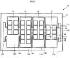
Fig. 1A is a top plan view of a light emitting apparatus according to an embodiment of the present invention; -
Fig. 1B is a cross-sectional view taken along aline 1B-1B ofFig. 1A ; -
Fig. 2A is a top plan view of a light emitting unit; -
Fig. 2B is a cross-sectional view of the light emitting unit; -
Fig. 3 is a diagram illustrating one example of a lighting unit using the light emitting apparatus; -
Fig. 4A is a top plan view of a light emitting unit according to a modified example; -
Fig. 4B is a cross-sectional view of the light emitting unit according to the modified example; -
Fig. 5 is a cross-sectional view of a light emitting apparatus according to a modified example; -
Fig. 6A is a top plan view of a light emitting unit according to a modified example; -
Fig. 6B is a top plan view of the light emitting unit according to the modified example; and -
Fig. 7 is a top plan view of a light emitting unit according to a modified example. - Preferred embodiments according to the present invention will be described hereinbelow. These embodiments may be appropriately modified or combined. In the following description and accompanying drawings, for the sake of explanation, the same reference numeral is assigned to identical or substantially identical elements.
- With reference to
Figs. 1A and 1B , alight emitting apparatus 10 according to an embodiment of the present invention will be described by way of an example of a light emitting apparatus using an LED device. Amounting substrate 11 is a rectangular planar substrate. Themounting substrate 11 includes a semiconductor, such as Si, a metal, such as Cu, or an insulating material, such as AlN or SiC. - A
substrate bonding layer 13 acting as a bonding layer is a metal layer formed by laminating Ti, Pt, and Au in this order on the upper surface of themounting substrate 11. Thesubstrate bonding layer 13 has: a plurality ofrectangular bonding regions 13A that are distanced from each other and arranged in a row on themounting substrate 11;connection regions 13B connecting the plurality ofrectangular bonding regions 13A; and apad region 13C that extends over theoutermost bonding regions 13A. Thebonding region 13A has a longer side in a direction perpendicular to the alignment direction thereof. The dashed line in the figure indicates a boundary between thebonding region 13A, theconnection region 13B, and thepad region 13C. - On each of the
bonding regions 13A of thesubstrate bonding layer 13 of themounting substrate 11, alight emitting unit 15 is disposed. Thelight emitting units 15 are arranged on themounting substrate 11 in a row. Thelight emitting unit 15 has asupport body 17 and a plurality oflight emitting devices 19 containing a semiconductor structure layer (not shown) with a light emitting layer (not shown), each of thelight emitting devices 19 being bonded to atop surface 17A of thesupport body 17. The illustrated example in the figure is configured such that fourlight emitting units 15 are arranged in a row. However, the number of thelight emitting units 15 may be smaller than or equal to three, or greater than or equal to five. In addition, thelight emitting units 15 may be arranged in two or more rows. - Each supporting
body 17 of thelight emitting unit 15 is formed from a conductive substrate of, for example, Si. The supportingbody 17 with a square columnar shape has a rectangular top surface (upper surface) 17A and a rectangular bottom surface (lower surface) 17B. The adjacent supportingbodies 17 are disposed so as to be distanced from each other. Specifically, a space SP is formed between the adjacent supportingbodies 17. - A bottom electrode (not shown) is formed by laminating Ti, Pt, and Au in this order on the
bottom surface 17B of the supportingbody 17 so as to cover thebottom surface 17B. The bottom electrode is bonded to the substrate bonding layer13 by means of thermo-compression, for example. A plurality oflight emitting devices 19 containing a semiconductor structure layer (not shown) with a light emitting layer (not shown) are formed on thetop surface 17A of the supportingbody 17. According to this embodiment, five light emittingdevices 19 are aligned in each of two rows in the alignment direction parallel with the longitudinal direction of the upper surface of the supportingbody 17. Specifically, thelight emitting devices 19 are arranged in two rows in the direction perpendicular to the alignment direction of thelight emitting units 15. - According to this embodiment, to form the
light emitting devices 19, a semiconductor layer containing a light emitting layer formed on a growth substrate (not shown) of, for example, sapphire is divided into a plurality of devices on the growth substrate, and after a plurality of the divided devices are attached to the supportingbodies 17, the growth substrate is removed. Thelight emitting unit 15 is a monolithic light emitting unit formed by integrating a plurality of thelight emitting devices 19 and the supportingbody 17. In other words, thelight emitting unit 15 is of a thin film LED structure. On the supportingbody 17, thelight emitting devices 19 can be located very close to each other. - The film thickness of the
light emitting device 19 thus formed, specifically, the thickness in the direction perpendicular to the upper surface of the supportingbody 17, can be 10 µm or smaller. Light guided from onelight emitting device 19 to the adjacentlight emitting device 19 can thereby be decreased. - It is preferable that the distance between the locations where the
light emitting devices 19 are arranged is as small as possible in the direction perpendicular to the alignment direction of thelight emitting units 15 so as to reduce a dark region (dark line) formed between the light emittingdevices 19. In the direction along the alignment direction of thelight emitting units 15, it is preferable to set a distance D1 between the adjacentlight emitting devices 19 within onelight emitting unit 15 on the basis of a distance D2 between adjacent light emittingdevices 19 in the adjacent respectivelight emitting units 15. It is more preferable to adjust the distance D1 so that the distances D1 and D2 are as equal as possible. - Due to, for example, the arrangement accuracy of the supporting
body 17, it is difficult to arrange the adjacentlight emitting devices 19 of the adjacent respectivelight emitting units 15 so that the distance therebetween is smaller than the distance between the adjacentlight emitting devices 19 within onelight emitting unit 15. In order for the distances D1 and D2 to be equal, thelight emitting devices 19 are disposed on the supportingbodies 17 by setting the distance D2 equal to the distance D1. By adjusting the distance D2 according to the distance D1, occurrence of luminance unevenness within thelight emitting apparatus 10 can be prevented. - It is a matter of course that the distance D2 between the adjacent
light emitting devices 19 of the adjacent respectivelight emitting units 15 may be adjusted according to the distance D1 between the adjacentlight emitting devices 19 within onelight emitting unit 15. This adjustment can be made by setting the distance D1 in advance and, according to the distance D1, adjusting the distance between the locations where thelight emitting units 15 are disposed. - A
phosphor layer 21 is formed so that thelight emitting portions 19 on the supportingbody 17 are buried under thephosphor layer 21. Specifically, thephosphor layer 21 is continuously formed on the plurality of light emittingunits 15 disposed on the mountingsubstrate 11 so as to entirely cover the plurality of light emittingunits 15. - The
phosphor layer 21 is, for example, a resin sheet containing phosphor particles and an amount of light scattering material. The phosphor particles used here are, for example, phosphor particles that is excited by blue light and emits yellow fluorescent light, such as Ce-activated yttrium-aluminum-garnet (YAG: Ce), Ce-activated terbium-aluminum-garnet (TAG: Ce), orthosilicate phosphor ((BaSrCa)SiO4, etc.), or α-SiAlON phosphor ((Ca-α-SiAlON)SiO4: Eu, etc.). The light scattering material is light scattering particles comprising, for example, TiO2, SiO2, ZnO, or Al2O3. - The
phosphor layer 21 may be formed by coating the supportingbody 17 with a liquid resin or glass binder containing a phosphor particle and a light scattering material and curing the coat on the supportingbody 17 by means of, for example, thermosetting. Thephosphor layer 21 may be formed of a plate containing a phosphor. Also, thephosphor layer 21 may be configured so that each light emittingdevice 19 is not buried under thephosphor layer 21 and thephosphor layer 21 is disposed above each light emittingdevice 19. -
Fig. 2A is a top plan view of onelight emitting unit 15.Fig. 2B is a cross-sectional view taken along aline 2B-2B ofFig. 2A . As described above, to form thelight emitting unit 15, a semiconductor layer formed on a growth substrate (not shown) of, for example, sapphire is divided into a plurality of devices on the growth substrate, and after the plurality of divided devices are attached to the supportingbodies 17, the growth substrate is removed. - As illustrated in
Figs. 2A and 2B , abottom electrode 23 is formed on the surface of the supportingbody 17 opposite to the surface on which thelight emitting elements 19 are disposed, i.e. , thebottom electrode 23 is formed on the lower surface of the supportingbody 17. Thebottom electrode 23 is formed by laminating Ti, Pt, and Au in this order on the surface of the supportingbody 17. When a Si substrate is used as the supportingbody 17, a thermal oxidation film on the lower surface of the supportingbody 17 is grinded or removed by means of wet etching prior to formation of thebottom electrode 23. - To mount the
light emitting unit 15 on the mountingsubstrate 11, for example, an AuSn paste is applied at the position on thesubstrate bonding layer 13 where thelight emitting unit 15 is to be mounted, and in turn thelight emitting unit 15 is mounted on the mountingsubstrate 11 so that thebottom electrode 23 is placed on the AuSn paste. Thereafter, thesubstrate bonding layer 13 and thebottom electrode 23 are bonded by means of heating. - On the upper surface of the supporting
body 17, an upper surface insulating layer 25serving as a first insulating layer formed from an insulating material, such as SiO2, is formed. When the supportingbody 17 is a Si substrate, the uppersurface insulating layer 25 may be a heat oxidation film formed on the surface of the Si substrate. - On the upper
surface insulating layer 25, a plurality ofindividual wirings 27 that are formed from a conductor, such as Au, are formed to be distanced from each other. Each of the plurality ofindividual wirings 27 extends from one end of the upper surface of the supportingbody 17 in the longitudinal direction to the region directly below each light emittingdevice 19. - The plurality of
individual wirings 27 each have one end exposed at one end of the upper surface of the supportingbody 17 in the longitudinal direction and the other end under thelight emitting device 19. At the exposed end of each of the plurality ofindividual wirings 27, there is provided anindividual wiring pad 27A that is formed from a conductor, such as Au, and can be electrically connected to an external element by means of, for example, wiring bonding. - On the upper
surface insulating layer 25 and theindividual wiring 27, aninterlayer insulating layer 29 serving as a second insulating layer formed from an insulating material, such as SiO2, is formed. In the region directly below each light emittingdevice 19, anopening 29H is formed in theinterlayer insulating layer 29. A part of the upper surface of theindividual wiring 27 is exposed through theopening 29H. The interlayer insulatinglayer 29 is not formed on theindividual wiring pad 27A. Specifically, theinterlayer insulating layer 29 is formed so as to cover theindividual wiring 27 on the upper insulatinglayer 25 while theindividual wiring pad 27A is exposed and the upper surface of theindividual wiring 27 is partially exposed in the region directly below thelight emitting device 19. - On the
interlayer insulating layer 29, a layeredcommon wiring 31 that is formed from a conductor, such as Au, and is commonly and electrically connected to each light emittingdevice 19 is formed. Thecommon wiring 31 is formed so as to circumvent theopening 29H. Specifically, theopening 29H and a surrounding region thereof are exposed from thecommon wiring 31. - A through
wiring 33 is formed from a conductor, such as Au, so as to be in contact with the surface of the supportingbody 17 in the region below any one of the light emitting devices 19 (the light emitting device in the center in the figures). Also, the throughwiring 33 is formed so as to penetrate through the uppersurface insulating layer 25 and the interlayer insulatinglayer 29 and reach the upper surface of the interlayer insulatinglayer 29. The throughwiring 33 is in contact with the supportingbody 17 and thecommon wiring 31 and electrically connects the supportingbody 17 to thecommon wiring 31. Two or more throughwirings 33 may be formed, and the throughwiring 33 may be formed in a region under two or more light emittingdevices 19. - Above the upper surface of the
individual wiring 27 exposed through theopening 29H, anindividual electrode 35 formed from a conductor, such as Au, is formed. Eachindividual electrode 35 is, for example, formed so as to be distanced from thecommon wiring 31 and thereby electrically insulated from thecommon wiring 31. - The
light emitting device 19 is bonded to thecommon wiring 31 and theindividual electrode 35 and formed above the supportingbody 17. Thelight emitting device 19 has asemiconductor structure layer 37 formed by laminating a p-type semiconductor layer 37A, alight emitting layer 37B, and an n-type semiconductor layer 37C in this order on the supportingbody 17. Thesemiconductor structure layer 37 has the composition of, for example, AlxInyGa1-x-yN (0 ≤ x ≤ 1, 0 ≤ y ≤ 1). - In the
semiconductor structure layer 37, a throughhole 37H is formed. The throughhole 37H originates from the surface of thesemiconductor structure layer 37 close to the supportingbody 17, i.e., from the surface of the p-type semiconductor layer 37A, and penetrates through the p-type semiconductor layer 37A and thelight emitting layer 37B to reach an inner portion of the n-type semiconductor layer 37C. The figure illustrates that only one throughhole 37H penetrating through each light emittingdevice 19, but in fact a plurality of the throughholes 37H are formed. - On the surface of the n-
type semiconductor layer 37C, aconical protrusion 37P (the structure surrounded by the dashed line in the figure) is formed. Through the surface of the n-type semiconductor layer 37C, theconical protrusion 37P is directed to efficiently releasing light emitted from thelight emitting layer 37B to the outside. Theconical protrusion 37P may be formed by immersing the surface of the n-type semiconductor layer 37C in an alkali solution, for example, a TMAH solution, to build an uneven or protrusion/depression structure derived from a semiconductor crystal structure on the surface of the n-type semiconductor layer 37C. Theconical protrusion 37P does not necessarily need to be formed. - A p-contact electrode 39 is formed by, for example, laminating Ag and TiW in this order on the surface of the p-
type semiconductor layer 37A. The p-contact electrode 39 is not formed on the peripheral edge region of the throughhole 37H on the surface of the p-type semiconductor layer 37A and the edge region on the surface of the p-type semiconductor layer 37A. Specifically, the peripheral edge region of the throughhole 37H and the edge region on the surface of the p-type semiconductor layer 37A are exposed from the p-contact electrode 39. - An insulating layer 41 is formed so as to cover the
semiconductor layer 37A, the p-contact electrode 39, and the side surface of the throughhole 37H. At the bottom of the throughhole 37H, the n-type semiconductor layer 37C is exposed from the insulating layer 41. In the insulating layer 41, a throughhole 41H that extends from the surface of the insulating layer 41 to the p-contact electrode 39 is formed. Specifically, a part of the p-contact electrode 39 is exposed from the insulating layer 41 through the throughhole 41H. - An n-
contact electrode 43 is formed in the throughhole 37H. The n-contact electrode 43 is formed from a metal material and is in contact with the surface of the n-type semiconductor layer 37C exposed from the insulating layer 41. The n-contact electrode 43 is, for example, formed so as to protrude from the surface of the insulating layer 41. - A p-
electrode 45 is formed in the throughhole 41H. The p-electrode 45 is in contact with the surface of the p-contact electrode 39 exposed from the insulating layer 41. The p-electrode 45 is formed by laminating Ti, Pt, and Au in this order on the surface of the p-contact electrode 39. The p-electrode 45 is formed so as to protrude from the insulating layer 41. - An n-
electrode 47 is formed on the surface of the insulating layer 41. The n-electrode 47 is formed by laminating Ti, Pt, and Au in this order on the surface of the insulating layer 41. The n-electrode 47 is formed so as to be distanced from the p-electrode 45. - The p-
electrode 45 and the n-electrode 47 are bonded to theindividual electrode 35 and thecommon electrode 31, respectively, formed on the supportingbody 17, by means of, for example, heat bonding in a vacuum environment. Specifically, theindividual electrode 35 and the p-electrode 45 are electrically connected to each other, and thecommon wiring 31 and the n-electrode 47 are electrically connected to each other. Accordingly, thelight emitting devices 19 are electrically connected in parallel between thepad portion 13A of thesubstrate bonding layer 13 and theindividual wiring pad 27A. Thelight emitting devices 19 can be individually driven by turning on and off the power of eachindividual wiring pad 27A. - As described above, to form the
light emitting apparatus 10, thelight emitting devices 19 are formed on the growth substrate and after thelight emitting devices 19 are attached on the supportingbody 17. Thelight emitting devices 19 can be formed on the supportingbody 17 so that the distance therebetween is very small within thelight emitting unit 15. Occurrence of a dark region (dark line) formed between the adjacentlight emitting devices 19 can thereby be reduced. - One
light emitting apparatus 10 according to the aforementioned embodiment is formed by arranging a plurality of thelight emitting units 15 including the supporting bodies, on each of which a plurality of thelight emitting devices 19 are formed. Onelight emitting apparatus 10 according to the aforementioned embodiment is not formed of onelight emitting unit 15 having a required number of light emitting devices. Instead, a light emitting apparatus having a required number of light emitting devices is formed by arranging a plurality of the separatelight emitting units 15. - When one light emitting apparatus is formed of one light emitting unit and the light emitting unit is partially defected, the light emitting unit having a number of light emitting devices required for the light emitting apparatus needs to be entirely replaced. Conversely, as in the case of the
light emitting apparatus 10 formed by arranging a plurality of thelight emitting units 15, when thelight emitting unit 15 is defected, only the defected unit needs to be replaced. The yield of thelight emitting apparatus 10 can thus be enhanced. - In the
light emitting apparatus 10 according to the aforementioned embodiment, a space SP (seeFig. 1 ) is formed between the adjacent supportingbodies 17 of the adjacentlight emitting units 15. Light that is emitted from thelight emitting device 19 of onelight emitting unit 15, propagates thorough thephosphor layer 21, and is destined to anotherlight emitting unit 15 adjacent the aforementioned onelight emitting unit 15 is attenuated after entering the space SP between the adjacent supportingbodies 17. Most of such light does not exit from the space SP. - Accordingly, light emitted from the
light emitting device 19 of onelight emitting unit 15 can be prevented from propagating through thephosphor layer 21 and leaking to the adjacentlight emitting unit 15. In particular, when thelight emitting devices 19 for using thelight emitting apparatus 10 for, for example, an adoptive driving beam (ADB: orientation variable head lamp) are separately driven, it is possible to reduce leakage of light to the adjacentlight emitting device 15, in other words, crosstalk of light. - In the present invention, the film thickness of the
light emitting device 19 can be 10 µm or smaller. The amount of light emitted from the sidewall of thelight emitting device 19 can be reduced, and crosstalk to an adjacent device can be further reduced. - As described above, the
light emitting apparatus 10 having a required number of thelight emitting devices 19 is formed by arranging a plurality of thelight emitting units 15 separate from each other. Thelight emitting devices 19, the number of which is required for thelight emitting apparatus 10, are distributed on a plurality of the supportingbodies 17 distanced from each other. Instead of disposing, on one supporting body, all light emitting devices required for the light emitting apparatus, the plane area of each supporting body is made smaller. A defect, such as a crack occurring to a supporting body due to difference in the coefficient of thermal expansion between the supporting body and a mounting substrate, can be prevented. - As illustrated above, in the
light emitting apparatus 10, thelight emitting devices 19 can be arranged very close to each other in the direction perpendicular to the alignment direction of thelight emitting units 15. A dark region (dark line) is rarely formed due to the space between the light emittingdevices 19 in the direction perpendicular to the alignment direction of the light emitting units. - When a dark region (dark line) of irradiation light is reduced by an optical system, such as a lens, arranged in the irradiation direction of the
light emitting apparatus 10, the optical system needs to address only a dark region (dark line) formed along the alignment direction of thelight emitting units 15. The structure of an optical system disposed on thelight emitting apparatus 10 can thus be simplified. -
Fig. 3 illustrates alighting unit 50 as one example of a lighting fixture using thelight emitting apparatus 10. In thelighting unit 50, the mountingsubstrate 11 is bonded to the surface of ametal substrate 51 to fix thelight emitting apparatus 10 to themetal substrate 51. In the light emitting direction (indicated by the white allow in the figure) of thelight emitting apparatus 10, alens 53 is disposed at a location opposite to the upper surface of thephosphor layer 21. A structure for enhancing heat dissipation, such as a heat dissipation fin, may be provided on themetal substrate 51 or attached as a separate body to themetal substrate 51. - As described above, when a dark region (dark line) of irradiation light from the
light emitting apparatus 10 is tried to be reduced, only a dark region (dark line) formed along the alignment direction of thelight emitting units 15 needs to be addressed. Thus, thelens 53 should be formed with a repetitive structure in which a plurality of cylindrical lenses are arranged so that images formed by light emitted from, for example, light emitting devices are overlapped with each other only in the alignment direction of thelight emitting units 15. - A structure for reducing a dark region (dark line) does not necessarily have to be provided in the direction perpendicular to the alignment direction of the
light emitting units 15. Employment of thelight emitting apparatus 10 enables use of a lens of a simple structure as thelens 53. - A description will now be given of an example where the
bottom electrode 23 is not used to supply power to thelight emitting device 19 of thelight emitting apparatus 10.Fig. 4A is a top plan view of alight emitting unit 15A of thelight emitting apparatus 10 according to the modified example 1.Fig. 4B is a cross-sectional view taken along aline 4B-4B ofFig. 4A . - The
light emitting unit 15A of the light emitting apparatus according to the modified example 1 is different from thelight emitting unit 15 according to the aforementioned embodiment in terms of the configuration of thecommon wiring 31. Another difference therebetween is that the throughwiring 33 is not disposed in thelight emitting unit 15A according to the modified example. Thelight emitting unit 15 according to the aforementioned embodiment and thelight emitting unit 15A of the according to the modified example are identical in terms of the other features. - A
common wiring pad 31A is disposed at the end portion of thecommon wiring 31 of thelight emitting unit 15A according to the modified example 1. The aforementioned end portion of thecommon wiring 31 is opposite to the end portion where theindividual wiring pad 27A is formed on the supportingbody 17. Thecommon wiring pad 31A is formed from a conductor, for example, Au and can be electrically connected to an external element by means of, for example, wire bonding. Specifically, in thelight emitting unit 15A according to the modified example 1, thelight emitting devices 19 are electrically connected in parallel between theindividual wiring pad 27A and thecommon wiring pad 31A. - In the
light emitting unit 15A according to the modified example 1, thebottom electrode 23 simply acts as a bonding layer with thebonding region 13A (seeFig. 1A ). In thelight emitting apparatus 10 that uses thelight emitting unit 15A according to the modified example 1, only thebonding region 13A needs to exist in thesubstrate bonding layer 13, and theconnection region 13B and thepad region 13C do not need to be formed. - In the
light emitting apparatus 10 that uses thelight emitting unit 15A according to the modified example 1, power supply via the supportingbody 17 is not necessary, and the supportingbody 17 does not need to be a conductive substrate. The supportingbody 17 may be an insulating substrate. When the supportingbody 17 is formed from an insulating substrate, the uppersurface insulating layer 25 does not need to be formed. - A description will now be given of an example which is different from the aforementioned embodiments in terms of the shape of the supporting
body 17.Fig. 5 is a cross-sectional view of thelight emitting apparatus 10 according to the modified example 2. As illustrated inFig. 5 , a notched recess portion C, which is notched from the side of thebottom surface 17B, is provided on the side surfaces of the supportingbody 17. The width of thebottom surface 17B of the supportingbody 17 is smaller than the width of thetop surface 17A thereof. The supportingbody 17 has an eave-shaped protrusion P that protrudes outwardly at the top portion in a direction parallel with thetop surface 17A. - In other words, in an area closer to the
top surface 17A, the supportingbody 17 has the protrusion P on the side surface along each adjacent region between the light emittingunits 15. - The distance between the side surfaces of the supporting
bodies 17 of the adjacentlight emitting units 15 is greater in the area near thetop surface 17A where the protrusion P is formed than the distance in the area where the protrusion P is not formed. In other words, the space between the adjacent supportingbodies 17 that is below the area where the protrusion P is formed is wider than the space between the protrusions P of the adjacent supportingbodies 17. This space defined by the protrusions P and the notched recess portions C functions as an escape of a flux eluted from a metal paste, such as AuSn, containing a flux used for bonding thelight emitting unit 15 and the mountingsubstrate 11. - Specifically, in manufacturing the
light emitting apparatus 10 according to the modified example 2, the space defined by the protrusions P and the notched recess portions C functions as an escape of a flux at the time of bonding thelight emitting unit 15 and the mountingsubstrate 11, and the space between the supportingbodies 17 is not completely filled with the flux. The stress acting on the side surface of the supportingbodies 17 by the eluted flux at the time of bonding is reduced. Thelight emitting unit 15 can be prevented from inclining or deviating from the positon where thelight emitting unit 15 is to be mounted during fusion bonding. - The above-described embodiments have been described with reference to the drawings with regard to the configuration of one
light emitting unit 15 where five light emittingdevices 19 of an identical size are arranged in each of two rows on the supportingbodies 17. However, thelight emitting devices 19 may be arranged differently. For example, thelight emitting devices 19 may be arranged in one or three or more rows in the direction perpendicular to the arrangement direction of thelight emitting units 15. In addition, thelight emitting devices 19 may have different sizes. For example, thelight emitting devices 19 may have different lengths in the direction perpendicular to the arrangement direction of thelight emitting units 15. -
Fig. 6A illustrates a modified example of arrangement of thelight emitting device 19. For example, when thelight emitting apparatus 10 is used as a light source of ADB, the light emitting region eventually needs to be finely changed at the central portion of thelight emitting apparatus 10. In such a case, for example, the lengths of thelight emitting devices 19 in the direction perpendicular to the alignment direction of thelight emitting units 15 may be set to decrease with a decrease in the distance of thelight emitting device 19 to a center axis AX, which runs along the alignment direction of thelight emitting units 15. As illustrated inFig. 6A , when the widths of thelight emitting devices 19 are denoted by L1, L2, and L3 in the ascending order of the distance of thelight emitting device 19 from the center axis AX, i.e., in the ascending order of the distance from the center position in the direction perpendicular to the alignment direction of the light emitting units, the widths of thelight emitting devices 19 may be set so that L1 < L2 < L3 holds true. - Also, the number of the
light emitting devices 19 may be changed for eachlight emitting unit 15. InFig. 6A , the number of thelight emitting devices 19 mounted on thelight emitting unit 15 is set to increase with a decrease in the distance of thelight emitting unit 15 to the center position of thelight emitting apparatus 10. It may be possible to configure so that the number of thelight emitting devices 19 increases as the distance to the center position decreases and that turning on and off is controlled for each smaller region. In this case as well, if necessary, the widths (lengths) of the light emitting devices may be set to decrease as the distance to a center axis C decreases. For example, when the widths of thelight emitting devices 19 are denoted by L4, L5, and L6 in the ascending order of the distance of thelight emitting device 19 from the center axis AX, the widths of thelight emitting devices 19 may be set so that L4 < L5 < L6 holds true. - As illustrated in
Fig. 6B , a smallestlight emitting device 19S may be disposed at a location distanced from the center positon of thelight emitting apparatus 10. The sizes (lengths) of thelight emitting devices 19 other than the smallestlight emitting device 19S increase with an increase in the distance from the smallestlight emitting device 19S. For example, the sizes of the otherlight emitting devices 19 may be set to constantly increase as the distance from the smallestlight emitting device 19S increases. The usedlight emitting units 15 are all the same. - When the
lighting unit 50 is formed of the aforementioned light emitting apparatus, the axis to be aligned with the optical axis of the lens is located at a position closer to the smallestlight emitting device 19S than to the center position of thelight emitting unit 15. - As illustrated in
Fig. 7 , thelight emitting units 15 with different sizes may be arranged. In this case, as illustrated inFig. 7 , thelight emitting units 15 may be offset from each other in the alignment direction of thelight emitting units 15. - In the above-described embodiments, examples of individually driving the
light emitting devices 19 have been described. However, by appropriately changing a wiring, thelight emitting devices 19 may be driven individually or entirely by the driving method or may be controlled so that thelight emitting devices 19 in a certain group are driven together. - In the above-described embodiments, examples where the
light emitting device 19 is an LED device have been described. However, thelight emitting device 19 may be another type of light emitting device, such as a vertical resonator-type light emitting diode. - In the above-described embodiments, examples where the
phosphor layer 21 is continuously formed over all thelight emitting units 15 have been described. However, the configuration of thephosphor layer 21 is not limited to these embodiments. For example, thephosphor layer 21 may be formed on each light emitting device, each row of light emitting devices in a light emitting unit, or each light emitting unit so that thephosphor layer 21 is separately formed. In this case, light shielding may be performed by filling a white resin, a black resin, or the like in each gap between the phosphor layers 21 thus formed. In this manner, thephosphor layer 21 is spread so as to reduce leakage of light from onelight emitting device 19 to the region of the adjacentlight emitting device 19, specifically, crosstalk of light. - Various numerical values, dimensions, materials, etc. as well as, for example, the configuration of a semiconductor structure layer or metal layer according to the aforementioned embodiments are merely for illustrative purposes. Different ones may be appropriately selected depending on, for example, the application and a semiconductor device to be manufactured.
Claims (7)
- A light emitting apparatus comprising:a mounting substrate;a plurality of supporting bodies disposed on the mounting substrate; anda plurality of light emitting devices disposed on upper surfaces of the plurality of supporting bodies,wherein the plurality of light emitting devices are arranged on each of plurality of supporting bodies in a plurality of rows in a direction perpendicular to an alignment direction of the plurality of supporting bodies.
- The light emitting apparatus according to claim 1, wherein
the plurality of light emitting devices are disposed in the alignment direction on one of the supporting bodies in a plurality of rows, and the adjacent light emitting devices in one of the supporting bodies are arranged in the alignment direction so that a distance therebetween is substantially equal to a distance between adjacent ones of the light emitting devices of the adjacent respective supporting bodies. - The light emitting apparatus according to claim 1 or 2, wherein
the plurality of light emitting devices have different lengths in the direction perpendicular to the alignment direction of the plurality of supporting bodies. - The light emitting apparatus according to claim 3, wherein
a length of the plurality of light emitting devices monotonically increases in the direction perpendicular to the alignment direction of the plurality of supporting bodies with an increase in a distance in the perpendicular direction to a light emitting device whose length is smallest in the perpendicular direction. - The light emitting apparatus according to claim 4, wherein
the plurality of light emitting devices on one of the supporting bodies are electrically connected with each other in parallel. - The light emitting apparatus according to claim 5, wherein
a film thickness of the plurality of light emitting devices is 10 µm or smaller. - The light emitting apparatus according to claim 6, further comprising:a phosphor layer continuously formed on all of the plurality of light emitting devices on at least one of the supporting bodies.
Applications Claiming Priority (1)
| Application Number | Priority Date | Filing Date | Title |
|---|---|---|---|
| JP2015229112A JP6782539B2 (en) | 2015-11-24 | 2015-11-24 | Light emitting device |
Publications (2)
| Publication Number | Publication Date |
|---|---|
| EP3174095A1 true EP3174095A1 (en) | 2017-05-31 |
| EP3174095B1 EP3174095B1 (en) | 2019-12-04 |
Family
ID=57394394
Family Applications (1)
| Application Number | Title | Priority Date | Filing Date |
|---|---|---|---|
| EP16200117.6A Active EP3174095B1 (en) | 2015-11-24 | 2016-11-22 | Light emitting apparatus |
Country Status (2)
| Country | Link |
|---|---|
| EP (1) | EP3174095B1 (en) |
| JP (1) | JP6782539B2 (en) |
Citations (5)
| Publication number | Priority date | Publication date | Assignee | Title |
|---|---|---|---|---|
| JP2009267423A (en) | 2002-04-12 | 2009-11-12 | Seoul Semiconductor Co Ltd | Light-emitting device |
| US20110026266A1 (en) * | 2008-04-22 | 2011-02-03 | Koito Manufacturing Co., Ltd. | Light source module and vehicle lamp |
| EP2341536A2 (en) * | 2009-12-24 | 2011-07-06 | Toshiba Lighting & Technology Corporation | Lighting apparatus |
| WO2012059837A1 (en) * | 2010-11-04 | 2012-05-10 | Koninklijke Philips Electronics N.V. | Solid state light emitting devices based on crystallographically relaxed structures |
| WO2015091005A1 (en) * | 2013-12-20 | 2015-06-25 | Osram Opto Semiconductors Gmbh | Optoelectronic semiconductor component and adaptive headlight for a motor vehicle |
Family Cites Families (6)
| Publication number | Priority date | Publication date | Assignee | Title |
|---|---|---|---|---|
| JP4432413B2 (en) * | 2003-09-05 | 2010-03-17 | 日亜化学工業株式会社 | Light source device and vehicle headlamp |
| JP2012169189A (en) * | 2011-02-15 | 2012-09-06 | Koito Mfg Co Ltd | Light-emitting module and vehicular lamp |
| DE102011056888A1 (en) * | 2011-12-22 | 2013-06-27 | Osram Opto Semiconductors Gmbh | Display device and method for producing a display device |
| DE102012222958A1 (en) * | 2012-12-12 | 2014-06-12 | Automotive Lighting Reutlingen Gmbh | Method and device for operating a lighting device of a motor vehicle |
| DE102012112302B4 (en) * | 2012-12-14 | 2026-03-26 | OSRAM Opto Semiconductors Gesellschaft mit beschränkter Haftung | Display device and method for manufacturing a display device |
| JP2015177028A (en) * | 2014-03-14 | 2015-10-05 | スタンレー電気株式会社 | Method of manufacturing semiconductor device |
-
2015
- 2015-11-24 JP JP2015229112A patent/JP6782539B2/en not_active Expired - Fee Related
-
2016
- 2016-11-22 EP EP16200117.6A patent/EP3174095B1/en active Active
Patent Citations (6)
| Publication number | Priority date | Publication date | Assignee | Title |
|---|---|---|---|---|
| JP2009267423A (en) | 2002-04-12 | 2009-11-12 | Seoul Semiconductor Co Ltd | Light-emitting device |
| JP2009296012A (en) | 2002-04-12 | 2009-12-17 | Seoul Semiconductor Co Ltd | Light emitting device |
| US20110026266A1 (en) * | 2008-04-22 | 2011-02-03 | Koito Manufacturing Co., Ltd. | Light source module and vehicle lamp |
| EP2341536A2 (en) * | 2009-12-24 | 2011-07-06 | Toshiba Lighting & Technology Corporation | Lighting apparatus |
| WO2012059837A1 (en) * | 2010-11-04 | 2012-05-10 | Koninklijke Philips Electronics N.V. | Solid state light emitting devices based on crystallographically relaxed structures |
| WO2015091005A1 (en) * | 2013-12-20 | 2015-06-25 | Osram Opto Semiconductors Gmbh | Optoelectronic semiconductor component and adaptive headlight for a motor vehicle |
Also Published As
| Publication number | Publication date |
|---|---|
| EP3174095B1 (en) | 2019-12-04 |
| JP2017098410A (en) | 2017-06-01 |
| JP6782539B2 (en) | 2020-11-11 |
Similar Documents
| Publication | Publication Date | Title |
|---|---|---|
| US10429011B2 (en) | Method of manufacturing light emitting device | |
| US10141491B2 (en) | Method of manufacturing light emitting device | |
| US9576941B2 (en) | Light-emitting device and method of manufacturing the same | |
| US12607906B2 (en) | Light-emitting device and method of manufacturing the same | |
| JP5554680B2 (en) | Light-emitting element mounting substrate, light-emitting device, and manufacturing method thereof | |
| EP2448028A2 (en) | Light emitting apparatus and production method thereof | |
| US10937770B2 (en) | Light-emitting device | |
| WO2005062389A2 (en) | Semiconductor light emitting device, lighting module, lighting apparatus, display element, and manufacturing method for semiconductor light emitting device | |
| JP2015126209A (en) | Light emitting device | |
| US20190267529A1 (en) | Light emitting element and light emitting device | |
| KR20190129178A (en) | Light emitting element package with thin film pad and manufacturing method thereof | |
| JP2013062416A (en) | Semiconductor light-emitting device and manufacturing method of the same | |
| US10937937B2 (en) | Optical semiconductor element | |
| US10396257B2 (en) | Method of manufacturing light emitting device | |
| US11056623B2 (en) | Light-emitting device and method of manufacturing light-emitting device | |
| JP6757173B2 (en) | Light emitting device | |
| EP3174095B1 (en) | Light emitting apparatus | |
| CN111009603A (en) | Light emitting device | |
| US11735687B2 (en) | Method of manufacturing light emitting device having a light-shielding frame around a light emitting surface | |
| JP2019117818A (en) | Mounting substrate, light emitting device, and manufacturing method of light emitting device | |
| CN113508463A (en) | Manufacturing method of light-emitting device and light-emitting module, and light-emitting device and light-emitting module | |
| US20230317688A1 (en) | Light-emitting device and manufacturing method of the same | |
| CN110959199B (en) | Optoelectronic semiconductor devices and methods for forming optoelectronic semiconductor devices |
Legal Events
| Date | Code | Title | Description |
|---|---|---|---|
| PUAI | Public reference made under article 153(3) epc to a published international application that has entered the european phase |
Free format text: ORIGINAL CODE: 0009012 |
|
| STAA | Information on the status of an ep patent application or granted ep patent |
Free format text: STATUS: THE APPLICATION HAS BEEN PUBLISHED |
|
| AK | Designated contracting states |
Kind code of ref document: A1 Designated state(s): AL AT BE BG CH CY CZ DE DK EE ES FI FR GB GR HR HU IE IS IT LI LT LU LV MC MK MT NL NO PL PT RO RS SE SI SK SM TR |
|
| AX | Request for extension of the european patent |
Extension state: BA ME |
|
| STAA | Information on the status of an ep patent application or granted ep patent |
Free format text: STATUS: REQUEST FOR EXAMINATION WAS MADE |
|
| 17P | Request for examination filed |
Effective date: 20171130 |
|
| RBV | Designated contracting states (corrected) |
Designated state(s): AL AT BE BG CH CY CZ DE DK EE ES FI FR GB GR HR HU IE IS IT LI LT LU LV MC MK MT NL NO PL PT RO RS SE SI SK SM TR |
|
| STAA | Information on the status of an ep patent application or granted ep patent |
Free format text: STATUS: EXAMINATION IS IN PROGRESS |
|
| 17Q | First examination report despatched |
Effective date: 20181127 |
|
| GRAP | Despatch of communication of intention to grant a patent |
Free format text: ORIGINAL CODE: EPIDOSNIGR1 |
|
| STAA | Information on the status of an ep patent application or granted ep patent |
Free format text: STATUS: GRANT OF PATENT IS INTENDED |
|
| INTG | Intention to grant announced |
Effective date: 20190705 |
|
| GRAS | Grant fee paid |
Free format text: ORIGINAL CODE: EPIDOSNIGR3 |
|
| GRAA | (expected) grant |
Free format text: ORIGINAL CODE: 0009210 |
|
| STAA | Information on the status of an ep patent application or granted ep patent |
Free format text: STATUS: THE PATENT HAS BEEN GRANTED |
|
| AK | Designated contracting states |
Kind code of ref document: B1 Designated state(s): AL AT BE BG CH CY CZ DE DK EE ES FI FR GB GR HR HU IE IS IT LI LT LU LV MC MK MT NL NO PL PT RO RS SE SI SK SM TR |
|
| REG | Reference to a national code |
Ref country code: GB Ref legal event code: FG4D |
|
| REG | Reference to a national code |
Ref country code: CH Ref legal event code: EP |
|
| REG | Reference to a national code |
Ref country code: AT Ref legal event code: REF Ref document number: 1210473 Country of ref document: AT Kind code of ref document: T Effective date: 20191215 |
|
| REG | Reference to a national code |
Ref country code: DE Ref legal event code: R096 Ref document number: 602016025451 Country of ref document: DE |
|
| REG | Reference to a national code |
Ref country code: IE Ref legal event code: FG4D |
|
| REG | Reference to a national code |
Ref country code: NL Ref legal event code: MP Effective date: 20191204 |
|
| REG | Reference to a national code |
Ref country code: LT Ref legal event code: MG4D |
|
| PG25 | Lapsed in a contracting state [announced via postgrant information from national office to epo] |
Ref country code: BG Free format text: LAPSE BECAUSE OF FAILURE TO SUBMIT A TRANSLATION OF THE DESCRIPTION OR TO PAY THE FEE WITHIN THE PRESCRIBED TIME-LIMIT Effective date: 20200304 Ref country code: FI Free format text: LAPSE BECAUSE OF FAILURE TO SUBMIT A TRANSLATION OF THE DESCRIPTION OR TO PAY THE FEE WITHIN THE PRESCRIBED TIME-LIMIT Effective date: 20191204 Ref country code: LV Free format text: LAPSE BECAUSE OF FAILURE TO SUBMIT A TRANSLATION OF THE DESCRIPTION OR TO PAY THE FEE WITHIN THE PRESCRIBED TIME-LIMIT Effective date: 20191204 Ref country code: SE Free format text: LAPSE BECAUSE OF FAILURE TO SUBMIT A TRANSLATION OF THE DESCRIPTION OR TO PAY THE FEE WITHIN THE PRESCRIBED TIME-LIMIT Effective date: 20191204 Ref country code: LT Free format text: LAPSE BECAUSE OF FAILURE TO SUBMIT A TRANSLATION OF THE DESCRIPTION OR TO PAY THE FEE WITHIN THE PRESCRIBED TIME-LIMIT Effective date: 20191204 Ref country code: GR Free format text: LAPSE BECAUSE OF FAILURE TO SUBMIT A TRANSLATION OF THE DESCRIPTION OR TO PAY THE FEE WITHIN THE PRESCRIBED TIME-LIMIT Effective date: 20200305 Ref country code: NO Free format text: LAPSE BECAUSE OF FAILURE TO SUBMIT A TRANSLATION OF THE DESCRIPTION OR TO PAY THE FEE WITHIN THE PRESCRIBED TIME-LIMIT Effective date: 20200304 |
|
| PG25 | Lapsed in a contracting state [announced via postgrant information from national office to epo] |
Ref country code: HR Free format text: LAPSE BECAUSE OF FAILURE TO SUBMIT A TRANSLATION OF THE DESCRIPTION OR TO PAY THE FEE WITHIN THE PRESCRIBED TIME-LIMIT Effective date: 20191204 Ref country code: RS Free format text: LAPSE BECAUSE OF FAILURE TO SUBMIT A TRANSLATION OF THE DESCRIPTION OR TO PAY THE FEE WITHIN THE PRESCRIBED TIME-LIMIT Effective date: 20191204 |
|
| PG25 | Lapsed in a contracting state [announced via postgrant information from national office to epo] |
Ref country code: AL Free format text: LAPSE BECAUSE OF FAILURE TO SUBMIT A TRANSLATION OF THE DESCRIPTION OR TO PAY THE FEE WITHIN THE PRESCRIBED TIME-LIMIT Effective date: 20191204 |
|
| PG25 | Lapsed in a contracting state [announced via postgrant information from national office to epo] |
Ref country code: NL Free format text: LAPSE BECAUSE OF FAILURE TO SUBMIT A TRANSLATION OF THE DESCRIPTION OR TO PAY THE FEE WITHIN THE PRESCRIBED TIME-LIMIT Effective date: 20191204 Ref country code: CZ Free format text: LAPSE BECAUSE OF FAILURE TO SUBMIT A TRANSLATION OF THE DESCRIPTION OR TO PAY THE FEE WITHIN THE PRESCRIBED TIME-LIMIT Effective date: 20191204 Ref country code: ES Free format text: LAPSE BECAUSE OF FAILURE TO SUBMIT A TRANSLATION OF THE DESCRIPTION OR TO PAY THE FEE WITHIN THE PRESCRIBED TIME-LIMIT Effective date: 20191204 Ref country code: RO Free format text: LAPSE BECAUSE OF FAILURE TO SUBMIT A TRANSLATION OF THE DESCRIPTION OR TO PAY THE FEE WITHIN THE PRESCRIBED TIME-LIMIT Effective date: 20191204 Ref country code: EE Free format text: LAPSE BECAUSE OF FAILURE TO SUBMIT A TRANSLATION OF THE DESCRIPTION OR TO PAY THE FEE WITHIN THE PRESCRIBED TIME-LIMIT Effective date: 20191204 Ref country code: PT Free format text: LAPSE BECAUSE OF FAILURE TO SUBMIT A TRANSLATION OF THE DESCRIPTION OR TO PAY THE FEE WITHIN THE PRESCRIBED TIME-LIMIT Effective date: 20200429 |
|
| PG25 | Lapsed in a contracting state [announced via postgrant information from national office to epo] |
Ref country code: SM Free format text: LAPSE BECAUSE OF FAILURE TO SUBMIT A TRANSLATION OF THE DESCRIPTION OR TO PAY THE FEE WITHIN THE PRESCRIBED TIME-LIMIT Effective date: 20191204 Ref country code: SK Free format text: LAPSE BECAUSE OF FAILURE TO SUBMIT A TRANSLATION OF THE DESCRIPTION OR TO PAY THE FEE WITHIN THE PRESCRIBED TIME-LIMIT Effective date: 20191204 Ref country code: IS Free format text: LAPSE BECAUSE OF FAILURE TO SUBMIT A TRANSLATION OF THE DESCRIPTION OR TO PAY THE FEE WITHIN THE PRESCRIBED TIME-LIMIT Effective date: 20200404 |
|
| REG | Reference to a national code |
Ref country code: DE Ref legal event code: R097 Ref document number: 602016025451 Country of ref document: DE |
|
| REG | Reference to a national code |
Ref country code: AT Ref legal event code: MK05 Ref document number: 1210473 Country of ref document: AT Kind code of ref document: T Effective date: 20191204 |
|
| PLBE | No opposition filed within time limit |
Free format text: ORIGINAL CODE: 0009261 |
|
| STAA | Information on the status of an ep patent application or granted ep patent |
Free format text: STATUS: NO OPPOSITION FILED WITHIN TIME LIMIT |
|
| PG25 | Lapsed in a contracting state [announced via postgrant information from national office to epo] |
Ref country code: DK Free format text: LAPSE BECAUSE OF FAILURE TO SUBMIT A TRANSLATION OF THE DESCRIPTION OR TO PAY THE FEE WITHIN THE PRESCRIBED TIME-LIMIT Effective date: 20191204 |
|
| 26N | No opposition filed |
Effective date: 20200907 |
|
| PG25 | Lapsed in a contracting state [announced via postgrant information from national office to epo] |
Ref country code: PL Free format text: LAPSE BECAUSE OF FAILURE TO SUBMIT A TRANSLATION OF THE DESCRIPTION OR TO PAY THE FEE WITHIN THE PRESCRIBED TIME-LIMIT Effective date: 20191204 Ref country code: AT Free format text: LAPSE BECAUSE OF FAILURE TO SUBMIT A TRANSLATION OF THE DESCRIPTION OR TO PAY THE FEE WITHIN THE PRESCRIBED TIME-LIMIT Effective date: 20191204 Ref country code: SI Free format text: LAPSE BECAUSE OF FAILURE TO SUBMIT A TRANSLATION OF THE DESCRIPTION OR TO PAY THE FEE WITHIN THE PRESCRIBED TIME-LIMIT Effective date: 20191204 |
|
| PG25 | Lapsed in a contracting state [announced via postgrant information from national office to epo] |
Ref country code: IT Free format text: LAPSE BECAUSE OF FAILURE TO SUBMIT A TRANSLATION OF THE DESCRIPTION OR TO PAY THE FEE WITHIN THE PRESCRIBED TIME-LIMIT Effective date: 20191204 |
|
| PG25 | Lapsed in a contracting state [announced via postgrant information from national office to epo] |
Ref country code: MC Free format text: LAPSE BECAUSE OF FAILURE TO SUBMIT A TRANSLATION OF THE DESCRIPTION OR TO PAY THE FEE WITHIN THE PRESCRIBED TIME-LIMIT Effective date: 20191204 |
|
| REG | Reference to a national code |
Ref country code: CH Ref legal event code: PL |
|
| PG25 | Lapsed in a contracting state [announced via postgrant information from national office to epo] |
Ref country code: LU Free format text: LAPSE BECAUSE OF NON-PAYMENT OF DUE FEES Effective date: 20201122 |
|
| REG | Reference to a national code |
Ref country code: BE Ref legal event code: MM Effective date: 20201130 |
|
| PG25 | Lapsed in a contracting state [announced via postgrant information from national office to epo] |
Ref country code: LI Free format text: LAPSE BECAUSE OF NON-PAYMENT OF DUE FEES Effective date: 20201130 Ref country code: CH Free format text: LAPSE BECAUSE OF NON-PAYMENT OF DUE FEES Effective date: 20201130 |
|
| PG25 | Lapsed in a contracting state [announced via postgrant information from national office to epo] |
Ref country code: IE Free format text: LAPSE BECAUSE OF NON-PAYMENT OF DUE FEES Effective date: 20201122 |
|
| PG25 | Lapsed in a contracting state [announced via postgrant information from national office to epo] |
Ref country code: TR Free format text: LAPSE BECAUSE OF FAILURE TO SUBMIT A TRANSLATION OF THE DESCRIPTION OR TO PAY THE FEE WITHIN THE PRESCRIBED TIME-LIMIT Effective date: 20191204 Ref country code: MT Free format text: LAPSE BECAUSE OF FAILURE TO SUBMIT A TRANSLATION OF THE DESCRIPTION OR TO PAY THE FEE WITHIN THE PRESCRIBED TIME-LIMIT Effective date: 20191204 Ref country code: CY Free format text: LAPSE BECAUSE OF FAILURE TO SUBMIT A TRANSLATION OF THE DESCRIPTION OR TO PAY THE FEE WITHIN THE PRESCRIBED TIME-LIMIT Effective date: 20191204 |
|
| PG25 | Lapsed in a contracting state [announced via postgrant information from national office to epo] |
Ref country code: MK Free format text: LAPSE BECAUSE OF FAILURE TO SUBMIT A TRANSLATION OF THE DESCRIPTION OR TO PAY THE FEE WITHIN THE PRESCRIBED TIME-LIMIT Effective date: 20191204 |
|
| PG25 | Lapsed in a contracting state [announced via postgrant information from national office to epo] |
Ref country code: BE Free format text: LAPSE BECAUSE OF NON-PAYMENT OF DUE FEES Effective date: 20201130 |
|
| REG | Reference to a national code |
Ref country code: DE Ref legal event code: R079 Ref document number: 602016025451 Country of ref document: DE Free format text: PREVIOUS MAIN CLASS: H01L0025075000 Ipc: H10H0029240000 |
|
| PGFP | Annual fee paid to national office [announced via postgrant information from national office to epo] |
Ref country code: FR Payment date: 20250930 Year of fee payment: 10 |
|
| PGFP | Annual fee paid to national office [announced via postgrant information from national office to epo] |
Ref country code: DE Payment date: 20250930 Year of fee payment: 10 |
|
| PGFP | Annual fee paid to national office [announced via postgrant information from national office to epo] |
Ref country code: GB Payment date: 20251001 Year of fee payment: 10 |