EP3173857A1 - Liquid crystal display device - Google Patents
Liquid crystal display device Download PDFInfo
- Publication number
- EP3173857A1 EP3173857A1 EP16201024.3A EP16201024A EP3173857A1 EP 3173857 A1 EP3173857 A1 EP 3173857A1 EP 16201024 A EP16201024 A EP 16201024A EP 3173857 A1 EP3173857 A1 EP 3173857A1
- Authority
- EP
- European Patent Office
- Prior art keywords
- liquid crystal
- sub
- electrode
- pixels
- bar
- Prior art date
- Legal status (The legal status is an assumption and is not a legal conclusion. Google has not performed a legal analysis and makes no representation as to the accuracy of the status listed.)
- Granted
Links
Images


Classifications
-
- G—PHYSICS
- G02—OPTICS
- G02F—OPTICAL DEVICES OR ARRANGEMENTS FOR THE CONTROL OF LIGHT BY MODIFICATION OF THE OPTICAL PROPERTIES OF THE MEDIA OF THE ELEMENTS INVOLVED THEREIN; NON-LINEAR OPTICS; FREQUENCY-CHANGING OF LIGHT; OPTICAL LOGIC ELEMENTS; OPTICAL ANALOGUE/DIGITAL CONVERTERS
- G02F1/00—Devices or arrangements for the control of the intensity, colour, phase, polarisation or direction of light arriving from an independent light source, e.g. switching, gating or modulating; Non-linear optics
- G02F1/01—Devices or arrangements for the control of the intensity, colour, phase, polarisation or direction of light arriving from an independent light source, e.g. switching, gating or modulating; Non-linear optics for the control of the intensity, phase, polarisation or colour
- G02F1/13—Devices or arrangements for the control of the intensity, colour, phase, polarisation or direction of light arriving from an independent light source, e.g. switching, gating or modulating; Non-linear optics for the control of the intensity, phase, polarisation or colour based on liquid crystals, e.g. single liquid crystal display cells
- G02F1/133—Constructional arrangements; Operation of liquid crystal cells; Circuit arrangements
- G02F1/1333—Constructional arrangements; Manufacturing methods
- G02F1/1343—Electrodes
- G02F1/134309—Electrodes characterised by their geometrical arrangement
-
- G—PHYSICS
- G02—OPTICS
- G02F—OPTICAL DEVICES OR ARRANGEMENTS FOR THE CONTROL OF LIGHT BY MODIFICATION OF THE OPTICAL PROPERTIES OF THE MEDIA OF THE ELEMENTS INVOLVED THEREIN; NON-LINEAR OPTICS; FREQUENCY-CHANGING OF LIGHT; OPTICAL LOGIC ELEMENTS; OPTICAL ANALOGUE/DIGITAL CONVERTERS
- G02F1/00—Devices or arrangements for the control of the intensity, colour, phase, polarisation or direction of light arriving from an independent light source, e.g. switching, gating or modulating; Non-linear optics
- G02F1/01—Devices or arrangements for the control of the intensity, colour, phase, polarisation or direction of light arriving from an independent light source, e.g. switching, gating or modulating; Non-linear optics for the control of the intensity, phase, polarisation or colour
- G02F1/13—Devices or arrangements for the control of the intensity, colour, phase, polarisation or direction of light arriving from an independent light source, e.g. switching, gating or modulating; Non-linear optics for the control of the intensity, phase, polarisation or colour based on liquid crystals, e.g. single liquid crystal display cells
- G02F1/133—Constructional arrangements; Operation of liquid crystal cells; Circuit arrangements
- G02F1/1333—Constructional arrangements; Manufacturing methods
- G02F1/1334—Constructional arrangements; Manufacturing methods based on polymer dispersed liquid crystals, e.g. microencapsulated liquid crystals
-
- G—PHYSICS
- G02—OPTICS
- G02F—OPTICAL DEVICES OR ARRANGEMENTS FOR THE CONTROL OF LIGHT BY MODIFICATION OF THE OPTICAL PROPERTIES OF THE MEDIA OF THE ELEMENTS INVOLVED THEREIN; NON-LINEAR OPTICS; FREQUENCY-CHANGING OF LIGHT; OPTICAL LOGIC ELEMENTS; OPTICAL ANALOGUE/DIGITAL CONVERTERS
- G02F1/00—Devices or arrangements for the control of the intensity, colour, phase, polarisation or direction of light arriving from an independent light source, e.g. switching, gating or modulating; Non-linear optics
- G02F1/01—Devices or arrangements for the control of the intensity, colour, phase, polarisation or direction of light arriving from an independent light source, e.g. switching, gating or modulating; Non-linear optics for the control of the intensity, phase, polarisation or colour
- G02F1/13—Devices or arrangements for the control of the intensity, colour, phase, polarisation or direction of light arriving from an independent light source, e.g. switching, gating or modulating; Non-linear optics for the control of the intensity, phase, polarisation or colour based on liquid crystals, e.g. single liquid crystal display cells
- G02F1/133—Constructional arrangements; Operation of liquid crystal cells; Circuit arrangements
- G02F1/1333—Constructional arrangements; Manufacturing methods
-
- G—PHYSICS
- G02—OPTICS
- G02F—OPTICAL DEVICES OR ARRANGEMENTS FOR THE CONTROL OF LIGHT BY MODIFICATION OF THE OPTICAL PROPERTIES OF THE MEDIA OF THE ELEMENTS INVOLVED THEREIN; NON-LINEAR OPTICS; FREQUENCY-CHANGING OF LIGHT; OPTICAL LOGIC ELEMENTS; OPTICAL ANALOGUE/DIGITAL CONVERTERS
- G02F1/00—Devices or arrangements for the control of the intensity, colour, phase, polarisation or direction of light arriving from an independent light source, e.g. switching, gating or modulating; Non-linear optics
- G02F1/01—Devices or arrangements for the control of the intensity, colour, phase, polarisation or direction of light arriving from an independent light source, e.g. switching, gating or modulating; Non-linear optics for the control of the intensity, phase, polarisation or colour
- G02F1/13—Devices or arrangements for the control of the intensity, colour, phase, polarisation or direction of light arriving from an independent light source, e.g. switching, gating or modulating; Non-linear optics for the control of the intensity, phase, polarisation or colour based on liquid crystals, e.g. single liquid crystal display cells
- G02F1/133—Constructional arrangements; Operation of liquid crystal cells; Circuit arrangements
- G02F1/1333—Constructional arrangements; Manufacturing methods
- G02F1/133377—Cells with plural compartments or having plurality of liquid crystal microcells partitioned by walls, e.g. one microcell per pixel
-
- G—PHYSICS
- G02—OPTICS
- G02F—OPTICAL DEVICES OR ARRANGEMENTS FOR THE CONTROL OF LIGHT BY MODIFICATION OF THE OPTICAL PROPERTIES OF THE MEDIA OF THE ELEMENTS INVOLVED THEREIN; NON-LINEAR OPTICS; FREQUENCY-CHANGING OF LIGHT; OPTICAL LOGIC ELEMENTS; OPTICAL ANALOGUE/DIGITAL CONVERTERS
- G02F1/00—Devices or arrangements for the control of the intensity, colour, phase, polarisation or direction of light arriving from an independent light source, e.g. switching, gating or modulating; Non-linear optics
- G02F1/01—Devices or arrangements for the control of the intensity, colour, phase, polarisation or direction of light arriving from an independent light source, e.g. switching, gating or modulating; Non-linear optics for the control of the intensity, phase, polarisation or colour
- G02F1/13—Devices or arrangements for the control of the intensity, colour, phase, polarisation or direction of light arriving from an independent light source, e.g. switching, gating or modulating; Non-linear optics for the control of the intensity, phase, polarisation or colour based on liquid crystals, e.g. single liquid crystal display cells
- G02F1/133—Constructional arrangements; Operation of liquid crystal cells; Circuit arrangements
- G02F1/1333—Constructional arrangements; Manufacturing methods
- G02F1/1335—Structural association of cells with optical devices, e.g. polarisers or reflectors
- G02F1/133509—Filters, e.g. light shielding masks
- G02F1/133514—Colour filters
-
- G—PHYSICS
- G02—OPTICS
- G02F—OPTICAL DEVICES OR ARRANGEMENTS FOR THE CONTROL OF LIGHT BY MODIFICATION OF THE OPTICAL PROPERTIES OF THE MEDIA OF THE ELEMENTS INVOLVED THEREIN; NON-LINEAR OPTICS; FREQUENCY-CHANGING OF LIGHT; OPTICAL LOGIC ELEMENTS; OPTICAL ANALOGUE/DIGITAL CONVERTERS
- G02F1/00—Devices or arrangements for the control of the intensity, colour, phase, polarisation or direction of light arriving from an independent light source, e.g. switching, gating or modulating; Non-linear optics
- G02F1/01—Devices or arrangements for the control of the intensity, colour, phase, polarisation or direction of light arriving from an independent light source, e.g. switching, gating or modulating; Non-linear optics for the control of the intensity, phase, polarisation or colour
- G02F1/13—Devices or arrangements for the control of the intensity, colour, phase, polarisation or direction of light arriving from an independent light source, e.g. switching, gating or modulating; Non-linear optics for the control of the intensity, phase, polarisation or colour based on liquid crystals, e.g. single liquid crystal display cells
- G02F1/133—Constructional arrangements; Operation of liquid crystal cells; Circuit arrangements
- G02F1/1333—Constructional arrangements; Manufacturing methods
- G02F1/1335—Structural association of cells with optical devices, e.g. polarisers or reflectors
- G02F1/133528—Polarisers
-
- G—PHYSICS
- G02—OPTICS
- G02F—OPTICAL DEVICES OR ARRANGEMENTS FOR THE CONTROL OF LIGHT BY MODIFICATION OF THE OPTICAL PROPERTIES OF THE MEDIA OF THE ELEMENTS INVOLVED THEREIN; NON-LINEAR OPTICS; FREQUENCY-CHANGING OF LIGHT; OPTICAL LOGIC ELEMENTS; OPTICAL ANALOGUE/DIGITAL CONVERTERS
- G02F1/00—Devices or arrangements for the control of the intensity, colour, phase, polarisation or direction of light arriving from an independent light source, e.g. switching, gating or modulating; Non-linear optics
- G02F1/01—Devices or arrangements for the control of the intensity, colour, phase, polarisation or direction of light arriving from an independent light source, e.g. switching, gating or modulating; Non-linear optics for the control of the intensity, phase, polarisation or colour
- G02F1/13—Devices or arrangements for the control of the intensity, colour, phase, polarisation or direction of light arriving from an independent light source, e.g. switching, gating or modulating; Non-linear optics for the control of the intensity, phase, polarisation or colour based on liquid crystals, e.g. single liquid crystal display cells
- G02F1/133—Constructional arrangements; Operation of liquid crystal cells; Circuit arrangements
- G02F1/1333—Constructional arrangements; Manufacturing methods
- G02F1/1343—Electrodes
- G02F1/134309—Electrodes characterised by their geometrical arrangement
- G02F1/134336—Matrix
-
- G—PHYSICS
- G02—OPTICS
- G02F—OPTICAL DEVICES OR ARRANGEMENTS FOR THE CONTROL OF LIGHT BY MODIFICATION OF THE OPTICAL PROPERTIES OF THE MEDIA OF THE ELEMENTS INVOLVED THEREIN; NON-LINEAR OPTICS; FREQUENCY-CHANGING OF LIGHT; OPTICAL LOGIC ELEMENTS; OPTICAL ANALOGUE/DIGITAL CONVERTERS
- G02F1/00—Devices or arrangements for the control of the intensity, colour, phase, polarisation or direction of light arriving from an independent light source, e.g. switching, gating or modulating; Non-linear optics
- G02F1/01—Devices or arrangements for the control of the intensity, colour, phase, polarisation or direction of light arriving from an independent light source, e.g. switching, gating or modulating; Non-linear optics for the control of the intensity, phase, polarisation or colour
- G02F1/13—Devices or arrangements for the control of the intensity, colour, phase, polarisation or direction of light arriving from an independent light source, e.g. switching, gating or modulating; Non-linear optics for the control of the intensity, phase, polarisation or colour based on liquid crystals, e.g. single liquid crystal display cells
- G02F1/133—Constructional arrangements; Operation of liquid crystal cells; Circuit arrangements
- G02F1/1333—Constructional arrangements; Manufacturing methods
- G02F1/1343—Electrodes
- G02F1/134309—Electrodes characterised by their geometrical arrangement
- G02F1/134363—Electrodes characterised by their geometrical arrangement for applying an electric field parallel to the substrate, i.e. in-plane switching [IPS]
-
- G—PHYSICS
- G02—OPTICS
- G02F—OPTICAL DEVICES OR ARRANGEMENTS FOR THE CONTROL OF LIGHT BY MODIFICATION OF THE OPTICAL PROPERTIES OF THE MEDIA OF THE ELEMENTS INVOLVED THEREIN; NON-LINEAR OPTICS; FREQUENCY-CHANGING OF LIGHT; OPTICAL LOGIC ELEMENTS; OPTICAL ANALOGUE/DIGITAL CONVERTERS
- G02F1/00—Devices or arrangements for the control of the intensity, colour, phase, polarisation or direction of light arriving from an independent light source, e.g. switching, gating or modulating; Non-linear optics
- G02F1/01—Devices or arrangements for the control of the intensity, colour, phase, polarisation or direction of light arriving from an independent light source, e.g. switching, gating or modulating; Non-linear optics for the control of the intensity, phase, polarisation or colour
- G02F1/13—Devices or arrangements for the control of the intensity, colour, phase, polarisation or direction of light arriving from an independent light source, e.g. switching, gating or modulating; Non-linear optics for the control of the intensity, phase, polarisation or colour based on liquid crystals, e.g. single liquid crystal display cells
- G02F1/133—Constructional arrangements; Operation of liquid crystal cells; Circuit arrangements
- G02F1/136—Liquid crystal cells structurally associated with a semi-conducting layer or substrate, e.g. cells forming part of an integrated circuit
- G02F1/1362—Active matrix addressed cells
- G02F1/136286—Wiring, e.g. gate line, drain line
-
- G—PHYSICS
- G02—OPTICS
- G02F—OPTICAL DEVICES OR ARRANGEMENTS FOR THE CONTROL OF LIGHT BY MODIFICATION OF THE OPTICAL PROPERTIES OF THE MEDIA OF THE ELEMENTS INVOLVED THEREIN; NON-LINEAR OPTICS; FREQUENCY-CHANGING OF LIGHT; OPTICAL LOGIC ELEMENTS; OPTICAL ANALOGUE/DIGITAL CONVERTERS
- G02F1/00—Devices or arrangements for the control of the intensity, colour, phase, polarisation or direction of light arriving from an independent light source, e.g. switching, gating or modulating; Non-linear optics
- G02F1/01—Devices or arrangements for the control of the intensity, colour, phase, polarisation or direction of light arriving from an independent light source, e.g. switching, gating or modulating; Non-linear optics for the control of the intensity, phase, polarisation or colour
- G02F1/13—Devices or arrangements for the control of the intensity, colour, phase, polarisation or direction of light arriving from an independent light source, e.g. switching, gating or modulating; Non-linear optics for the control of the intensity, phase, polarisation or colour based on liquid crystals, e.g. single liquid crystal display cells
- G02F1/133—Constructional arrangements; Operation of liquid crystal cells; Circuit arrangements
- G02F1/136—Liquid crystal cells structurally associated with a semi-conducting layer or substrate, e.g. cells forming part of an integrated circuit
- G02F1/1362—Active matrix addressed cells
- G02F1/1368—Active matrix addressed cells in which the switching element is a three-electrode device
-
- G—PHYSICS
- G02—OPTICS
- G02F—OPTICAL DEVICES OR ARRANGEMENTS FOR THE CONTROL OF LIGHT BY MODIFICATION OF THE OPTICAL PROPERTIES OF THE MEDIA OF THE ELEMENTS INVOLVED THEREIN; NON-LINEAR OPTICS; FREQUENCY-CHANGING OF LIGHT; OPTICAL LOGIC ELEMENTS; OPTICAL ANALOGUE/DIGITAL CONVERTERS
- G02F1/00—Devices or arrangements for the control of the intensity, colour, phase, polarisation or direction of light arriving from an independent light source, e.g. switching, gating or modulating; Non-linear optics
- G02F1/01—Devices or arrangements for the control of the intensity, colour, phase, polarisation or direction of light arriving from an independent light source, e.g. switching, gating or modulating; Non-linear optics for the control of the intensity, phase, polarisation or colour
- G02F1/13—Devices or arrangements for the control of the intensity, colour, phase, polarisation or direction of light arriving from an independent light source, e.g. switching, gating or modulating; Non-linear optics for the control of the intensity, phase, polarisation or colour based on liquid crystals, e.g. single liquid crystal display cells
- G02F1/133—Constructional arrangements; Operation of liquid crystal cells; Circuit arrangements
- G02F1/1333—Constructional arrangements; Manufacturing methods
- G02F1/1335—Structural association of cells with optical devices, e.g. polarisers or reflectors
- G02F1/133528—Polarisers
- G02F1/133531—Polarisers characterised by the arrangement of polariser or analyser axes
-
- G—PHYSICS
- G02—OPTICS
- G02F—OPTICAL DEVICES OR ARRANGEMENTS FOR THE CONTROL OF LIGHT BY MODIFICATION OF THE OPTICAL PROPERTIES OF THE MEDIA OF THE ELEMENTS INVOLVED THEREIN; NON-LINEAR OPTICS; FREQUENCY-CHANGING OF LIGHT; OPTICAL LOGIC ELEMENTS; OPTICAL ANALOGUE/DIGITAL CONVERTERS
- G02F1/00—Devices or arrangements for the control of the intensity, colour, phase, polarisation or direction of light arriving from an independent light source, e.g. switching, gating or modulating; Non-linear optics
- G02F1/01—Devices or arrangements for the control of the intensity, colour, phase, polarisation or direction of light arriving from an independent light source, e.g. switching, gating or modulating; Non-linear optics for the control of the intensity, phase, polarisation or colour
- G02F1/13—Devices or arrangements for the control of the intensity, colour, phase, polarisation or direction of light arriving from an independent light source, e.g. switching, gating or modulating; Non-linear optics for the control of the intensity, phase, polarisation or colour based on liquid crystals, e.g. single liquid crystal display cells
- G02F1/133—Constructional arrangements; Operation of liquid crystal cells; Circuit arrangements
- G02F1/1333—Constructional arrangements; Manufacturing methods
- G02F1/1343—Electrodes
- G02F1/134309—Electrodes characterised by their geometrical arrangement
- G02F1/134345—Subdivided pixels, e.g. for grey scale or redundancy
-
- G—PHYSICS
- G02—OPTICS
- G02F—OPTICAL DEVICES OR ARRANGEMENTS FOR THE CONTROL OF LIGHT BY MODIFICATION OF THE OPTICAL PROPERTIES OF THE MEDIA OF THE ELEMENTS INVOLVED THEREIN; NON-LINEAR OPTICS; FREQUENCY-CHANGING OF LIGHT; OPTICAL LOGIC ELEMENTS; OPTICAL ANALOGUE/DIGITAL CONVERTERS
- G02F1/00—Devices or arrangements for the control of the intensity, colour, phase, polarisation or direction of light arriving from an independent light source, e.g. switching, gating or modulating; Non-linear optics
- G02F1/01—Devices or arrangements for the control of the intensity, colour, phase, polarisation or direction of light arriving from an independent light source, e.g. switching, gating or modulating; Non-linear optics for the control of the intensity, phase, polarisation or colour
- G02F1/13—Devices or arrangements for the control of the intensity, colour, phase, polarisation or direction of light arriving from an independent light source, e.g. switching, gating or modulating; Non-linear optics for the control of the intensity, phase, polarisation or colour based on liquid crystals, e.g. single liquid crystal display cells
- G02F1/133—Constructional arrangements; Operation of liquid crystal cells; Circuit arrangements
- G02F1/136—Liquid crystal cells structurally associated with a semi-conducting layer or substrate, e.g. cells forming part of an integrated circuit
- G02F1/1362—Active matrix addressed cells
- G02F1/13624—Active matrix addressed cells having more than one switching element per pixel
-
- G—PHYSICS
- G02—OPTICS
- G02F—OPTICAL DEVICES OR ARRANGEMENTS FOR THE CONTROL OF LIGHT BY MODIFICATION OF THE OPTICAL PROPERTIES OF THE MEDIA OF THE ELEMENTS INVOLVED THEREIN; NON-LINEAR OPTICS; FREQUENCY-CHANGING OF LIGHT; OPTICAL LOGIC ELEMENTS; OPTICAL ANALOGUE/DIGITAL CONVERTERS
- G02F2201/00—Constructional arrangements not provided for in groups G02F1/00 - G02F7/00
- G02F2201/52—RGB geometrical arrangements
-
- G—PHYSICS
- G02—OPTICS
- G02F—OPTICAL DEVICES OR ARRANGEMENTS FOR THE CONTROL OF LIGHT BY MODIFICATION OF THE OPTICAL PROPERTIES OF THE MEDIA OF THE ELEMENTS INVOLVED THEREIN; NON-LINEAR OPTICS; FREQUENCY-CHANGING OF LIGHT; OPTICAL LOGIC ELEMENTS; OPTICAL ANALOGUE/DIGITAL CONVERTERS
- G02F2202/00—Materials and properties
- G02F2202/36—Micro- or nanomaterials
Definitions
- the present invention relates to a liquid crystal display device (LCD).
- LCD liquid crystal display device
- the present invention relates to an LCD including a nano capsule liquid crystal layer.
- LCD liquid crystal display device
- PDP plasma display panel device
- ELD electroluminescent display device
- FED field emission display device
- CRT cathode ray tube
- LCDs are most widely used in the fields of a laptop, monitor, television (TV) because they are excellent in displaying moving images and a high contrast ratio.
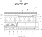
- FIG. 1 is a cross-sectional view illustrating an LCD according to a related art.
- the related art LCD 10 includes a liquid crystal panel having a first substrate 2 and a second substrate 4 attached to each other with a liquid crystal layer 50 therebetween, and a backlight 60.
- a thin film transistor Tr on the first substrate 2 includes a gate electrode 12, a gate insulating layer 13, an active layer 14, ohmic contact layers 15a and 15b, and source and drain electrodes 16 and 17, and is connected to a first electrode 19 in a pixel region P through a contact hole formed in an inter-layered insulating film 18.
- a black matrix 32 is below the second substrate 4, and has a lattice shape to surround the pixel region P such that the black matrix 32 shields a non-display element such as the thin film transistor Tr and exposes the first electrode 19.
- a color filter 34 is arranged in the lattice-shaped black matrix 32 corresponding to the pixel region P, and a second electrode is arranged to cover the black matrix 32 and the color filter 34.
- Polarizing plates 20 and 30 each selectively transmitting a predetermined polarized light are attached below the first substrate 2 and on the second substrate 4, respectively. Further, a first alignment layer 31a having a surface rubbed in a predetermined direction is between the liquid crystal layer 50 and the first electrode 19, and a second alignment layer 31b having a surface rubbed in a predetermined direction is between the liquid crystal layer 50 and the second electrode 36, and thus initial arrangement state and alignment direction of liquid crystal molecules are uniform. Further, to prevent a leakage of the liquid crystal layer 50, a seal pattern 70 is arranged along edge portions of the first and second substrates 2 and 4. Since the LCD 10 is not self-luminescent, the backlight 60 as a light source is arranged below the liquid crystal panel to supply light to the liquid crystal panel.
- a nematic liquid crystal, a smetic liquid crystal, a cholesteric liquid crystal or the like is used, and the nematic liquid crystal is mostly used.
- an alignment process when attaching the two substrates 2 and 4 is additionally required after the substrates 2 and 4 are individually manufactured. Further, processes of printing and rubbing the alignment layers 31a and 31b to align the liquid crystal are required, and due to these processes, production rate is reduced.
- a gap between the two substrates 2 and 4 needs to be maintained after attaching the substrates 2 and 4 and injecting the liquid crystal between the substrates 2 and 4, and if a gap between the two substrates changes by an external pressure or impact, display quality may be degraded.
- the present invention is directed to an LCD that substantially obviates one or more of the problems due to limitations and disadvantages of the related art.
- An object of the present invention is to provide an LCD that can prevent a phenomenon of a non-uniform color coordinate.
- a liquid crystal display device includes a substrate including a unit pixel having first to third sub-pixels arranged in a delta structure; and a first electrode and a second electrode in each of the first to third sub-pixels, each of the first and second electrodes including a first bar and a plurality of second bars branching off from the first bar (e.g., forming respective fork-like patterns), the first bar of the first electrode and the first bar of the second electrode facing each other and being parallel with each other, the second bars of the first electrode and the second bars of the second electrode interleaved with each other, wherein the first and second bars of the third sub-pixel makes first and second angles, respectively, relative to a first polarization axis.
- the first bar of each of the first and second sub-pixels is parallel with the first polarization axis
- the second bar of the first sub-pixel is parallel with the first or second bar of the third sub-pixel
- the second bar of the second sub-pixel is parallel with the second or first bar of the third sub-pixel.
- the first and second angles are the same in absolute value.
- the first and second angles are 45 degree angles relative to the first polarization axis.
- each of the first and second sub-pixels has a parallelogram shape
- the third sub-pixel has a rhombus shape
- the unit pixel has a hexagon shape.
- the first to third sub-pixels have the same area and have the same distance between the corresponding second bars of the first to third sub-pixels.
- the liquid crystal display device further comprises first and second thin film transistors connected to the first and second electrodes, respectively.
- the liquid crystal display device further comprises: a nano capsule liquid crystal layer that is on and contacts the first and second electrodes; a first polarizing plate below the substrate and having the first polarization axis; and a second polarizing plate that is on and contacts the nano capsule liquid crystal layer, and has a second polarization axis perpendicular to the first polarization axis.
- the nano capsule liquid crystal layer is configured in a film type.
- the nano capsule liquid crystal layer includes a plurality of nano capsules that are dispersed in a buffer layer.
- a nano capsule of the plurality of nano capsules has a size less than wavelengths of visible light and is filled with liquid crystal molecules randomly aligned.
- At least one of the first and second sub-pixels includes a blue color filter, and the third sub-pixel includes a red or green color filter.
- the liquid crystal display device further comprises: a first data line and a second data line for the first to third sub-pixels, the first data line supplying a first data voltage to a respective first electrode, the second data line supplying a second data voltage to a respective second electrode, wherein the second data voltage has a level opposite to a level of the first data voltage.
- a liquid crystal display device comprises: a substrate including a unit pixel of a delta structure including first to third sub-pixels; a first electrode and a second electrode formed on the substrate in each of the first to third sub-pixels; a nano capsule liquid crystal layer on the first and second electrodes; and a first polarizing plate below the substrate and a second polarizing plate directly on the nano capsule liquid crystal layer, wherein the unit pixel has a hexagon shape.
- each of the first and second electrodes includes a first bar and a plurality of second bars branching off from the first bar (e.g., forming respective fork-like patterns), the first bar of the first electrode and the first bar of the second electrode facing each other and being parallel with each other, the second bars of the first electrode and the second bars of the second electrode interleaved with each other, and the first and second bars of the third sub-pixel make first and second angles, respectively, relative to a first polarization axis.
- the liquid crystal display device further comprises: a first data line and a second data line for the first to third sub-pixels, the first data line supplying a first data voltage to a respective first electrode, the second data line supplying a second data voltage to a respective second electrode, wherein the second data voltage has a level opposite to a level of the first data voltage.
- At least one of the first and second sub-pixels includes a blue color filter, and the third sub-pixel includes a red or green color filter.
- the nano capsule liquid crystal layer is configured in a film type.
- the nano capsule liquid crystal layer includes a plurality of nano capsules that are dispersed in a buffer layer.
- a nano capsule of the plurality of nano capsules has a size less than wavelengths of visible light and is filled with liquid crystal molecules randomly aligned.
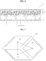
- FIG. 2 is a cross-sectional view illustrating an LCD 100 according to an embodiment of the present invention.
- the LCD 100 of the embodiment includes a substrate 101, first and second electrodes 120 and 130 on the substrate 101, a nano capsule liquid crystal layer 140 on the first and second electrodes 120 and 130, and first and second polarizing plates 150 and 160 that are below the substrate 101 and directly on the nano capsule liquid crystal layer 140, respectively.
- the nano capsule liquid crystal layer 140 is formed with nano capsules 142 that are dispersed in a buffer layer 143.
- Each nano capsule 142 may have a size less than wavelength of a visible light, e.g., no more than 320 nm, and is filled with liquid crystal molecules 141 randomly aligned.
- the nano capsule liquid crystal layer 140 including the nano capsules 142, the liquid crystal molecules 141 within the nano capsules 142, and the buffer layer 143 may be formed using a variety of formation methods, such as a printing method, a coating method, or a dropping method.
- the nano capsule liquid crystal layer 140 may be formed in a film type over the first and second electrodes 120 and 130. Accordingly, unlike the related art LCD using two substrates, the LCD 100 of this embodiment can be manufactured with one substrate 101, and thus the LCD of light weight and thin profile can be achieved, and production cost can be reduced.
- the nano capsule liquid crystal layer 140 does not have the problem of the related art that the gap between the related art two substrates becomes non-uniform or changes by an external pressure or impact.
- the nano capsule liquid crystal layer 140 can be effectively applied to a flexible LCD.
- the nano capsule liquid crystal layer 140 has an optical isotropy when an electric field is not applied.
- the nano capsule liquid crystal layer 140 has an optical property that when an electric field is applied, the liquid crystal molecules 141 in the nano capsule 142 are aligned in a direction of the electric field and birefringence of a light incident on the nano capsule liquid crystal layer 140 is produced. Accordingly, the nano capsule liquid crystal layer 140 can form an optical axis according to an applied electric field, and by controlling an optical property using this, a light can be transmitted.
- the first polarizing plate 150 produces a polarization of a light to be incident on the nano capsule liquid crystal layer 140 from the backlight 170.
- the second polarizing plate 160 blocks a light that is incident on the nano capsule liquid crystal layer 140 and then passes through the nano capsule liquid crystal layer 140 without polarization by a birefringence effect of the nano capsule liquid crystal layer 140.
- a polarization axis of the first polarizing plate 150 and a polarization axis of the second polarizing plate 160 are perpendicular to each other. For example, if the polarization axis of the first polarizing plate 150 has a 0 or 90 degree angle, the polarization axis of the second polarization plate 160 has a 90 or 0 degree angle.
- a principle of operating the LCD 100 including the nano capsule liquid crystal layer 140 is explained below. First, when an electric field is not induced between the first and second electrodes 120 and 130, the nano capsule liquid crystal layer 140 passes through a light entering it through the first polarizing plate 150, and thus the LCD 100 displays a black state.
- a light entering the first polarizing plate 150 from the backlight 170 is selectively transmitted at a specific angle while passing through the first polarization plate 150, then the light entering the nano capsule liquid crystal layer 140 is transmitted through the nano capsule liquid crystal layer 140 with a minimal scattering phenomenon and then reaches the second polarizing plate 160.
- a light passing through the first polarization plate 150 having a polarization axis of, for example, a 0 degree angle enters the second polarization plate 160 having the polarization axis of, for example, a 90 degree angle, thus this light is blocked by the second polarizing plate 160 perpendicular in polarizing axis to the first polarizing plate 150, and thus the LCD 100 displays the black state.
- the LCD 100 of this embodiment can display the black state using the optical property of the nano capsule liquid crystal layer 140 and thus does not require an additional process of aligning a liquid crystal. Accordingly, the LCD 100 of this embodiment can eliminate processes of printing and rubbing an alignment layer that the related art LCD necessarily requires.
- the nano capsule liquid crystal layer 140 may contact the first and second electrodes 120 and 130 without an alignment layer therebetween, and may contact the second polarization plate 160 without an alignment layer therebetween.
- the nano capsule liquid crystal layer 140 rotates a polarization axis of a light entering the nano capsule liquid crystal layer 140 through the first polarization plate 150 by a 90 degree angle, and thus the LCD 100 displays a white state.
- the LCD 100 displays a white state.
- the liquid crystal molecules 141 in the nano capsule 142 are arranged in parallel with a direction of the electric field, a birefringence effect by the alignment of the liquid crystal molecules 141 is produced.
- a light entering the nano capsule liquid crystal layer 140 through the first polarizing plate 150 changes in polarization by the birefringence effect of the nano capsule liquid crystal layer 140.
- a retardation, ⁇ n*d, of the nano capsule liquid crystal layer 140 meets a ⁇ /2 condition of a light incident thereon, a polarization axis of the incident light is rotated by 90 degree angle, thus this light is not absorbed by the second polarizing plate 160 perpendicular in polarization axis to the first polarizing plate 150 and passes through the second polarizing plate 160, and thus the LCD 100 displays the white state.
- the LCD 100 including the nano capsule liquid crystal layer 140 controls a light transmission amount through a refractive index of the nano capsule liquid crystal layer 140
- liquid crystal molecules having two or three times the refractive index of the liquid crystal molecules of the related art is required.
- a liquid crystal molecule having a greater refractive index has a greater wavelength dispersion property, a problem may occur that a color coordinate goes awry (e.g., becomes non-uniform) when displaying images and thus a white balance is not achieved.
- an LCD has a property that a refractive index inducement of a short wavelength is produced more than that of a long wavelength when operating the LCD in the same operation condition (electrode, voltage and the like), and because of this property, an efficiency of a blue region is greater than that of a red region. Accordingly, a color coordinate is biased to a blue side, and thus a problem may happen that a bluish image is displayed.
- FIG. 3 is a view illustrating unit pixels of an LCD according to the embodiment of the present invention.
- a unit pixel 200 includes first to third sub-pixels SP1 to SP3 arranged in a delta ( ⁇ ) structure.
- the first to third sub-pixels SP1 to SP3 may display red, green and blue, respectively, and these sub-pixels SP1 to SP3 constitute one unit pixel 200.
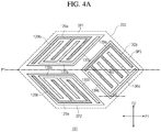
- FIGS. 4A and 4B are views illustrating electrode arrangement structures of sub-pixels of a unit pixel of FIG. 3 .
- the LCD of this embodiment includes a substrate 101 including a unit pixel 200, of a delta ( ⁇ ) structure, having first to third sub-pixels SP1 to SP3, and first and second electrodes 120 and 130 arranged in each of the first to third sub-pixels SP1 to SP3.
- the first electrode 120 includes a first bar 120a and a plurality of second bars 120b branching off from the first bar 120a forming a fork-like pattern
- the second electrode 130 includes a first bar 130a and a plurality of second bars 130b branching off from the first bar 130a forming a fork-like pattern.
- the first bar 120a of the first electrode 120 faces and is parallel with the first bar 130a of the second electrode 130
- the second bars 120b of the first electrode 120 are interleaved with the second bars 130b of the second electrode 130 (e.g., the second bars 120b and 130b may alternate).
- Electric fields between the first and second bars 120a and 120b of the first electrode 120 and the first and second bars 130a and 130b of the second electrode 130 are produced at the shortest distances between the first and second bars 120a and 120b of the first electrode 120 and the first and second bars 130a and 130b of the second electrode 130, and when an electric field distribution aligns with a first polarization axis P1 or a second polarization axis P2 perpendicular to the first polarization axis P1, a light transmittance is minimized.
- the first bars 120a and 130a, and the second bars 120b and 130b of the third sub-pixel SP3 make a first angle ⁇ 1, and a second angle ⁇ 2, respectively, relative to the first polarization axis P1, thus distributions of electric fields between the first and second bars 120a and 120b of the first electrode 120 and the first and second bars 130a and 130 of the second electrode 130 maximally un-aligns with the first and second polarization axes P1 and P2, and thus a light transmittance can be maximized.
- first angle ⁇ 1 and the second angle ⁇ 2 may be the same in absolute value, and in order that distributions of electric fields between the first and second bars 120a and 120b of the first electrode 120 and the first and second bars 130a and 130b of the second electrode 130 maximally disaccord with the first and second polarization axes P1 and P2, each of the first angle ⁇ 1 and the second angle ⁇ 2 may be a 45 degree angle. Further, the first bars 120a and 130a of the first and second sub-pixels SP1 and SP2 are arranged parallel with the first polarization axis P1.
- the second bars 120b and 130b of the first sub-pixel SP1 are parallel with the first bars 120a and 130a of the third sub-pixel SP3, and the second bars 120b and 130b of the second sub-pixel SP2 are parallel with the second bars 120b and 130b of the third sub-pixel SP3.
- the second bars 120b and 130b of the first sub-pixel SP1 are parallel with the second bars 120b and 130b of the third sub-pixel SP3, and the second bars 120b and 130b of the second sub-pixel SP2 are parallel with the first bars 120a and 130a of the third sub-pixel SP3.
- the LCD of this embodiment uses liquid crystal molecules having two or three times the refractive index of the related art liquid crystal molecules, by arranging a color filter requiring a relatively greater light transmittance at the third sub-pixel SP3 that has a light transmittance greater than the first and second sub-pixels SP1 and SP2, and arranging a color filter requiring a relatively less light transmittance at the first or second sub-pixel SP1 or SP2, a color coordinate becomes uniform when displaying images and thus a white balance can be achieved.
- FIG. 5 is a view illustrating a pixel arrangement produced with a plurality of unit pixels according to the embodiment of the present invention.
- the first and second electrodes 120 and 130 are arranged as above, the first and second sub-pixels SP1 and SP2 each have a parallelogram shape, the third sub-pixel SP3 has a rhombus shape, and the unit pixel 200 consisting of the first to third sub-pixels SP1 to SP3 has a hexagon shape.
- the first to third sub-pixels SP1 to SP3 of the delta ( ⁇ ) structure may display green (G), blue (B) and red (R), respectively, and these sub-pixels SP1 to SP3 constitute one unit pixel 200.
- G green
- B blue
- R red
- these sub-pixels SP1 to SP3 constitute one unit pixel 200.
- two neighboring unit pixels 200 share the third sub-pixel SP3, and thus more natural image can be displayed.
- FIG. 6 is a view schematically illustrating the second sub-pixel of FIGS. 4A and 4B . Since the first to third sub-pixels SP1 to SP3 have the same components and the same relationship between the same components, the second sub-pixel SP2 are representatively explained.
- the LCD 100 of this embodiment includes a gate line GL on a substrate 101, first and second data lines DL1 and DL2 crossing the gate line GL to define the second sub-pixel SP2, first and second electrodes 120 and 130 located in the second sub-pixel SP2, and first and second thin film transistors Tr1 and Tr2.
- the first electrode 120 includes a first bar 120a and a plurality of second bars 120b branching off from the first bar 120a forming a fork-like pattern
- the second electrode 130 includes a first bar 130a and a plurality of second bars 130b branching off from the first bar 130a forming a fork-like pattern.
- the first bar 120a of the first electrode 120 faces and is parallel with the first bar 130a of the second electrode 130
- the second bars 120b of the first electrode 120 are interleaved with the second bars 130b of the second electrode 130 (e.g., the second bars 120b and 130b may alternate).
- first thin film transistor Tr1 is connected to the gate line GL and the first data line DL1 and supplies a first data voltage to the first electrode 120.
- the second thin film transistor Tr2 is connected to the gate line GL and the second data line DL2 and supplies a second data voltage, which has a level opposite to a level of the first data voltage, to the second electrode 130.
- the first thin film transistor Tr1 includes a gate electrode G connected to the gate line GL, a source electrode S connected to the first data line DL1, and a drain electrode D connected to the first electrode 120.
- the second thin film transistor Tr2 includes a gate electrode G connected to the gate line GL, a source electrode S connected to the second data line DL2, and a drain electrode D connected to the second electrode 130.
- a method of driving the LCD is explained with reference to FIG. 6 .
- the first data voltage is supplied from the first data line DL1 to the first electrode 120 alternating between positive and negative voltages with respect to a constant common voltage
- the second data voltage having a level opposite to the level of the first data voltage is supplied from the second data line DL2 to the second electrode 130.
- FIG. 7 is a graph illustrating a relative light transmittance to a relative voltage applied to each sub-pixel of the embodiment of the present invention.
- FIG. 8 is a view illustrating brightness by area of each sub-pixel according to the embodiment of the present invention.
- a light transmittance of the third sub-pixel SP3 is greater than those of the first and second sub-pixels SP1 and SP2. Accordingly, referring to FIG. 8 , a dark state of the third sub-pixel SP3 is minimized compared with the first and second sub-pixels SP1 and SP2.
- the first and second sub-pixels SP1 and SP2 are greater than the third sub-pixel SP3.
- the third sub-pixel SP3 has a light transmittance greater than the first and second sub-pixels SP1 and SP2.
- a uniform color coordinate when displaying images and a white balance can be achieved, and particularly, it a color coordinate that is biased to a blue side and display of a bluish image can be prevented.
- one or more features described above in one embodiment or example can be equally applied to another embodiment or example described above.
- the features of one or more embodiments or examples described above can be combined into each of the embodiments or examples described above. Any full or partial combination of one or more embodiment or examples of the invention is also part of the invention.
Landscapes
- Physics & Mathematics (AREA)
- Nonlinear Science (AREA)
- Chemical & Material Sciences (AREA)
- Mathematical Physics (AREA)
- Crystallography & Structural Chemistry (AREA)
- General Physics & Mathematics (AREA)
- Optics & Photonics (AREA)
- Geometry (AREA)
- Engineering & Computer Science (AREA)
- Microelectronics & Electronic Packaging (AREA)
- Dispersion Chemistry (AREA)
- Liquid Crystal (AREA)
Abstract
Description
- The present application claims the priority benefit of the Korean Patent Application No.
10-2015-0169515 - The present invention relates to a liquid crystal display device (LCD). In particular, the present invention relates to an LCD including a nano capsule liquid crystal layer.
- With the advancement of information society, the display field of displaying electric information signals has been rapidly advanced. Accordingly, as flat display devices having advantages of thin profile, light weight and low power consumption, including a liquid crystal display device (LCD), a plasma display panel device (PDP), an electroluminescent display device (ELD), a field emission display device (FED) and the like have been introduced and have rapidly replaced a conventional cathode ray tube (CRT). Among the flat display devices, LCDs are most widely used in the fields of a laptop, monitor, television (TV) because they are excellent in displaying moving images and a high contrast ratio.
-
FIG. 1 is a cross-sectional view illustrating an LCD according to a related art. Referring toFIG. 1 , therelated art LCD 10 includes a liquid crystal panel having afirst substrate 2 and asecond substrate 4 attached to each other with aliquid crystal layer 50 therebetween, and abacklight 60. - In detail, a thin film transistor Tr on the
first substrate 2 includes agate electrode 12, agate insulating layer 13, anactive layer 14,ohmic contact layers drain electrodes first electrode 19 in a pixel region P through a contact hole formed in an inter-layeredinsulating film 18. Further, ablack matrix 32 is below thesecond substrate 4, and has a lattice shape to surround the pixel region P such that theblack matrix 32 shields a non-display element such as the thin film transistor Tr and exposes thefirst electrode 19. Further, acolor filter 34 is arranged in the lattice-shapedblack matrix 32 corresponding to the pixel region P, and a second electrode is arranged to cover theblack matrix 32 and thecolor filter 34. - Polarizing
plates first substrate 2 and on thesecond substrate 4, respectively. Further, afirst alignment layer 31a having a surface rubbed in a predetermined direction is between theliquid crystal layer 50 and thefirst electrode 19, and asecond alignment layer 31b having a surface rubbed in a predetermined direction is between theliquid crystal layer 50 and thesecond electrode 36, and thus initial arrangement state and alignment direction of liquid crystal molecules are uniform. Further, to prevent a leakage of theliquid crystal layer 50, aseal pattern 70 is arranged along edge portions of the first andsecond substrates LCD 10 is not self-luminescent, thebacklight 60 as a light source is arranged below the liquid crystal panel to supply light to the liquid crystal panel. - As the liquid crystal layer for the
LCD 10, a nematic liquid crystal, a smetic liquid crystal, a cholesteric liquid crystal or the like is used, and the nematic liquid crystal is mostly used. However, in therelated art LCD 10, there is an disadvantage that an alignment process when attaching the twosubstrates substrates alignment layers substrates substrates substrates - Accordingly, the present invention is directed to an LCD that substantially obviates one or more of the problems due to limitations and disadvantages of the related art. An object of the present invention is to provide an LCD that can prevent a phenomenon of a non-uniform color coordinate.
- Additional features and advantages of the disclosure will be set forth in the description which follows, and in part will be apparent from the description, or may be learned by practice of the disclosure. The advantages of the disclosure will be realized and attained by the structure particularly pointed out in the written description and claims as well as the appended drawings.
- To achieve these and other advantages, and in accordance with the purpose of the present invention, as embodied and broadly described herein, a liquid crystal display device includes a substrate including a unit pixel having first to third sub-pixels arranged in a delta structure; and a first electrode and a second electrode in each of the first to third sub-pixels, each of the first and second electrodes including a first bar and a plurality of second bars branching off from the first bar (e.g., forming respective fork-like patterns), the first bar of the first electrode and the first bar of the second electrode facing each other and being parallel with each other, the second bars of the first electrode and the second bars of the second electrode interleaved with each other, wherein the first and second bars of the third sub-pixel makes first and second angles, respectively, relative to a first polarization axis.
- In one or more embodiments, the first bar of each of the first and second sub-pixels is parallel with the first polarization axis, the second bar of the first sub-pixel is parallel with the first or second bar of the third sub-pixel, and the second bar of the second sub-pixel is parallel with the second or first bar of the third sub-pixel.
- In one or more embodiments, the first and second angles are the same in absolute value.
- In one or more embodiments, the first and second angles are 45 degree angles relative to the first polarization axis.
- In one or more embodiments, each of the first and second sub-pixels has a parallelogram shape, the third sub-pixel has a rhombus shape, and the unit pixel has a hexagon shape.
- In one or more embodiments, the first to third sub-pixels have the same area and have the same distance between the corresponding second bars of the first to third sub-pixels.
- In one or more embodiments, the liquid crystal display device further comprises first and second thin film transistors connected to the first and second electrodes, respectively.
- In one or more embodiments, the liquid crystal display device further comprises: a nano capsule liquid crystal layer that is on and contacts the first and second electrodes; a first polarizing plate below the substrate and having the first polarization axis; and a second polarizing plate that is on and contacts the nano capsule liquid crystal layer, and has a second polarization axis perpendicular to the first polarization axis.
- In one or more embodiments, the nano capsule liquid crystal layer is configured in a film type.
- In one or more embodiments, the nano capsule liquid crystal layer includes a plurality of nano capsules that are dispersed in a buffer layer.
- In one or more embodiments, a nano capsule of the plurality of nano capsules has a size less than wavelengths of visible light and is filled with liquid crystal molecules randomly aligned.
- In one or more embodiments, at least one of the first and second sub-pixels includes a blue color filter, and the third sub-pixel includes a red or green color filter.
- In one or more embodiments, the liquid crystal display device further comprises: a first data line and a second data line for the first to third sub-pixels, the first data line supplying a first data voltage to a respective first electrode, the second data line supplying a second data voltage to a respective second electrode, wherein the second data voltage has a level opposite to a level of the first data voltage.
- According to another aspect of the present disclosure, a liquid crystal display device comprises: a substrate including a unit pixel of a delta structure including first to third sub-pixels; a first electrode and a second electrode formed on the substrate in each of the first to third sub-pixels; a nano capsule liquid crystal layer on the first and second electrodes; and a first polarizing plate below the substrate and a second polarizing plate directly on the nano capsule liquid crystal layer, wherein the unit pixel has a hexagon shape.
- In one or more embodiments, each of the first and second electrodes includes a first bar and a plurality of second bars branching off from the first bar (e.g., forming respective fork-like patterns), the first bar of the first electrode and the first bar of the second electrode facing each other and being parallel with each other, the second bars of the first electrode and the second bars of the second electrode interleaved with each other, and the first and second bars of the third sub-pixel make first and second angles, respectively, relative to a first polarization axis.
- In one or more embodiments, the liquid crystal display device further comprises: a first data line and a second data line for the first to third sub-pixels, the first data line supplying a first data voltage to a respective first electrode, the second data line supplying a second data voltage to a respective second electrode, wherein the second data voltage has a level opposite to a level of the first data voltage.
- In one or more embodiments, at least one of the first and second sub-pixels includes a blue color filter, and the third sub-pixel includes a red or green color filter.
- In one or more embodiments, the nano capsule liquid crystal layer is configured in a film type.
- In one or more embodiments, the nano capsule liquid crystal layer includes a plurality of nano capsules that are dispersed in a buffer layer.
- In one or more embodiments, a nano capsule of the plurality of nano capsules has a size less than wavelengths of visible light and is filled with liquid crystal molecules randomly aligned.
- It is to be understood that both the foregoing general description and the following detailed description are exemplary and explanatory and are intended to provide further explanation of the invention as claimed.
- The accompanying drawings, which are included to provide a further understanding of the disclosure and are incorporated in and constitute a part of this specification, illustrate embodiments of the disclosure and together with the description serve to explain the principles of the disclosure. In the drawings:
-
FIG. 1 is a cross-sectional view illustrating an LCD according to the related art; -
FIG. 2 is a cross-sectional view illustrating an LCD according to an embodiment of the present invention; -
FIG. 3 is a view illustrating unit pixels of an LCD according to the embodiment of the present invention; -
FIGS. 4A and4B are views illustrating electrode arrangement structures of sub-pixels of a unit pixel ofFIG. 3 ; -
FIG. 5 is a view illustrating a pixel arrangement produced with a plurality of unit pixels according to the embodiment of the present invention; -
FIG. 6 is a view schematically illustrating the second sub-pixel ofFIGS. 4A and4B ; -
FIG. 7 is a graph illustrating a relative light transmittance to a relative voltage applied to each sub-pixel of the embodiment of the present invention; and -
FIG. 8 is a view illustrating brightness by area of each sub-pixel according to the embodiment of the present invention. - Reference will now be made in detail to embodiments, examples of which are illustrated in the accompanying drawings. The same or like reference numbers may be used throughout the drawings to refer to the same or like parts.
-
FIG. 2 is a cross-sectional view illustrating anLCD 100 according to an embodiment of the present invention. Referring toFIG. 2 , theLCD 100 of the embodiment includes asubstrate 101, first andsecond electrodes substrate 101, a nano capsule liquid crystal layer 140 on the first andsecond electrodes polarizing plates substrate 101 and directly on the nano capsule liquid crystal layer 140, respectively. - The nano capsule liquid crystal layer 140 is formed with nano capsules 142 that are dispersed in a buffer layer 143. Each nano capsule 142 may have a size less than wavelength of a visible light, e.g., no more than 320 nm, and is filled with
liquid crystal molecules 141 randomly aligned. The nano capsule liquid crystal layer 140 including the nano capsules 142, theliquid crystal molecules 141 within the nano capsules 142, and the buffer layer 143 may be formed using a variety of formation methods, such as a printing method, a coating method, or a dropping method. The nano capsule liquid crystal layer 140 may be formed in a film type over the first andsecond electrodes LCD 100 of this embodiment can be manufactured with onesubstrate 101, and thus the LCD of light weight and thin profile can be achieved, and production cost can be reduced. - Further, the nano capsule liquid crystal layer 140 does not have the problem of the related art that the gap between the related art two substrates becomes non-uniform or changes by an external pressure or impact. Thus, when forming the
substrate 101 using a flexible material such as a plastic, the nano capsule liquid crystal layer 140 can be effectively applied to a flexible LCD. - Further, the nano capsule liquid crystal layer 140 has an optical isotropy when an electric field is not applied. However, the nano capsule liquid crystal layer 140 has an optical property that when an electric field is applied, the
liquid crystal molecules 141 in the nano capsule 142 are aligned in a direction of the electric field and birefringence of a light incident on the nano capsule liquid crystal layer 140 is produced. Accordingly, the nano capsule liquid crystal layer 140 can form an optical axis according to an applied electric field, and by controlling an optical property using this, a light can be transmitted. - Further, the first
polarizing plate 150 produces a polarization of a light to be incident on the nano capsule liquid crystal layer 140 from thebacklight 170. The secondpolarizing plate 160 blocks a light that is incident on the nano capsule liquid crystal layer 140 and then passes through the nano capsule liquid crystal layer 140 without polarization by a birefringence effect of the nano capsule liquid crystal layer 140. - A polarization axis of the first
polarizing plate 150 and a polarization axis of the secondpolarizing plate 160 are perpendicular to each other. For example, if the polarization axis of the firstpolarizing plate 150 has a 0 or 90 degree angle, the polarization axis of thesecond polarization plate 160 has a 90 or 0 degree angle. - A principle of operating the
LCD 100 including the nano capsule liquid crystal layer 140 is explained below. First, when an electric field is not induced between the first andsecond electrodes polarizing plate 150, and thus theLCD 100 displays a black state. - In other words, in the off state with no electric field being applied, a light entering the first
polarizing plate 150 from thebacklight 170 is selectively transmitted at a specific angle while passing through thefirst polarization plate 150, then the light entering the nano capsule liquid crystal layer 140 is transmitted through the nano capsule liquid crystal layer 140 with a minimal scattering phenomenon and then reaches the secondpolarizing plate 160. Finally, a light passing through thefirst polarization plate 150 having a polarization axis of, for example, a 0 degree angle enters thesecond polarization plate 160 having the polarization axis of, for example, a 90 degree angle, thus this light is blocked by the secondpolarizing plate 160 perpendicular in polarizing axis to the firstpolarizing plate 150, and thus theLCD 100 displays the black state. - As described above, unlike the related art LCD requiring that a pair of alignment layers are arranged on a pair of substrates opposing to each other, respectively, and a liquid crystal is injected between the substrates and is aligned to have predetermined pitch and direction, the
LCD 100 of this embodiment can display the black state using the optical property of the nano capsule liquid crystal layer 140 and thus does not require an additional process of aligning a liquid crystal. Accordingly, theLCD 100 of this embodiment can eliminate processes of printing and rubbing an alignment layer that the related art LCD necessarily requires. In this embodiment, the nano capsule liquid crystal layer 140 may contact the first andsecond electrodes second polarization plate 160 without an alignment layer therebetween. - When an electric field is induced between the first and
second electrodes first polarization plate 150 by a 90 degree angle, and thus theLCD 100 displays a white state. In detail, in the on state with the electric field being induced, since theliquid crystal molecules 141 in the nano capsule 142 are arranged in parallel with a direction of the electric field, a birefringence effect by the alignment of theliquid crystal molecules 141 is produced. - In this case, a light entering the nano capsule liquid crystal layer 140 through the first
polarizing plate 150 changes in polarization by the birefringence effect of the nano capsule liquid crystal layer 140. When a retardation, Δn*d, of the nano capsule liquid crystal layer 140 meets a λ/2 condition of a light incident thereon, a polarization axis of the incident light is rotated by 90 degree angle, thus this light is not absorbed by the secondpolarizing plate 160 perpendicular in polarization axis to the firstpolarizing plate 150 and passes through the secondpolarizing plate 160, and thus theLCD 100 displays the white state. - Since the
LCD 100 including the nano capsule liquid crystal layer 140 controls a light transmission amount through a refractive index of the nano capsule liquid crystal layer 140, liquid crystal molecules having two or three times the refractive index of the liquid crystal molecules of the related art is required. However, since a liquid crystal molecule having a greater refractive index has a greater wavelength dispersion property, a problem may occur that a color coordinate goes awry (e.g., becomes non-uniform) when displaying images and thus a white balance is not achieved. - Further, according to a Kerr effect, an LCD has a property that a refractive index inducement of a short wavelength is produced more than that of a long wavelength when operating the LCD in the same operation condition (electrode, voltage and the like), and because of this property, an efficiency of a blue region is greater than that of a red region. Accordingly, a color coordinate is biased to a blue side, and thus a problem may happen that a bluish image is displayed. Features of this embodiment to resolve the above problems are explained below.
-
FIG. 3 is a view illustrating unit pixels of an LCD according to the embodiment of the present invention. Referring toFIG. 3 , aunit pixel 200 includes first to third sub-pixels SP1 to SP3 arranged in a delta (Δ) structure. The first to third sub-pixels SP1 to SP3 may display red, green and blue, respectively, and these sub-pixels SP1 to SP3 constitute oneunit pixel 200. -
FIGS. 4A and4B are views illustrating electrode arrangement structures of sub-pixels of a unit pixel ofFIG. 3 . First, referring toFIGS. 4A and4B , the LCD of this embodiment includes asubstrate 101 including aunit pixel 200, of a delta (Δ) structure, having first to third sub-pixels SP1 to SP3, and first andsecond electrodes - In detail, the
first electrode 120 includes afirst bar 120a and a plurality ofsecond bars 120b branching off from thefirst bar 120a forming a fork-like pattern, and thesecond electrode 130 includes afirst bar 130a and a plurality ofsecond bars 130b branching off from thefirst bar 130a forming a fork-like pattern. Further, thefirst bar 120a of thefirst electrode 120 faces and is parallel with thefirst bar 130a of thesecond electrode 130, and thesecond bars 120b of thefirst electrode 120 are interleaved with thesecond bars 130b of the second electrode 130 (e.g., thesecond bars - Electric fields between the first and
second bars first electrode 120 and the first andsecond bars second electrode 130 are produced at the shortest distances between the first andsecond bars first electrode 120 and the first andsecond bars second electrode 130, and when an electric field distribution aligns with a first polarization axis P1 or a second polarization axis P2 perpendicular to the first polarization axis P1, a light transmittance is minimized. - Accordingly, in the
LCD 100 of this embodiment, thefirst bars second bars second bars first electrode 120 and the first andsecond bars second electrode 130 maximally un-aligns with the first and second polarization axes P1 and P2, and thus a light transmittance can be maximized. - Further, the first angle θ1 and the second angle θ2 may be the same in absolute value, and in order that distributions of electric fields between the first and
second bars first electrode 120 and the first andsecond bars second electrode 130 maximally disaccord with the first and second polarization axes P1 and P2, each of the first angle θ1 and the second angle θ2 may be a 45 degree angle. Further, thefirst bars - Further, referring to
FIG. 4A , thesecond bars first bars second bars second bars FIG. 4B , thesecond bars second bars second bars first bars - In this case, distributions of electric fields between the
second bars 120b of thefirst electrode 120 and thesecond bars 130b of thesecond electrode 130, in the first and second sub-pixels SP1 and SP2, maximally un-aligns with the first and second polarization axes P1 and P2, and thus a light transmittance is maximized. However, distributions of electric field between thefirst bar 120a of thefirst electrode 120 and thesecond bars 130b of thesecond electrode 130, and between thefirst bar 130a of thesecond electrode 130 and thesecond bars 120b of thefirst electrode 120 align with the first or second polarization axis P1 or P2, and thus a transmittance is minimized. - Accordingly, even though the LCD of this embodiment uses liquid crystal molecules having two or three times the refractive index of the related art liquid crystal molecules, by arranging a color filter requiring a relatively greater light transmittance at the third sub-pixel SP3 that has a light transmittance greater than the first and second sub-pixels SP1 and SP2, and arranging a color filter requiring a relatively less light transmittance at the first or second sub-pixel SP1 or SP2, a color coordinate becomes uniform when displaying images and thus a white balance can be achieved.
- Particularly, by placing a blue color filter at the first or second sub-pixel SP1 or SP2 and placing a red or green color filter at the third sub-pixel SP3, a color coordinate that is biased to a blue side and display of a bluish image can be prevented. To obtain the above advantage, in the related art, by forming sub-pixels that are different in an electrode interval and an area, light transmittance is adjusted. However, forming sub-pixels in this manner may produce a display defect due to light diffraction. Thus, in this embodiment, along the above-described advantage, by forming the first to third sub-pixels SP1 to SP3 having the same area and the same distance between the
second bars -
FIG. 5 is a view illustrating a pixel arrangement produced with a plurality of unit pixels according to the embodiment of the present invention. When the first andsecond electrodes unit pixel 200 consisting of the first to third sub-pixels SP1 to SP3 has a hexagon shape. - Further, referring to
FIG. 5 , the first to third sub-pixels SP1 to SP3 of the delta (Δ) structure may display green (G), blue (B) and red (R), respectively, and these sub-pixels SP1 to SP3 constitute oneunit pixel 200. In this case, among the plurality ofunit pixels 200, two neighboringunit pixels 200 share the third sub-pixel SP3, and thus more natural image can be displayed. -
FIG. 6 is a view schematically illustrating the second sub-pixel ofFIGS. 4A and4B . Since the first to third sub-pixels SP1 to SP3 have the same components and the same relationship between the same components, the second sub-pixel SP2 are representatively explained. Referring toFIG. 6 , theLCD 100 of this embodiment includes a gate line GL on asubstrate 101, first and second data lines DL1 and DL2 crossing the gate line GL to define the second sub-pixel SP2, first andsecond electrodes - In detail, the
first electrode 120 includes afirst bar 120a and a plurality ofsecond bars 120b branching off from thefirst bar 120a forming a fork-like pattern, and thesecond electrode 130 includes afirst bar 130a and a plurality ofsecond bars 130b branching off from thefirst bar 130a forming a fork-like pattern. Further, thefirst bar 120a of thefirst electrode 120 faces and is parallel with thefirst bar 130a of thesecond electrode 130, and thesecond bars 120b of thefirst electrode 120 are interleaved with thesecond bars 130b of the second electrode 130 (e.g., thesecond bars - Further, the first thin film transistor Tr1 is connected to the gate line GL and the first data line DL1 and supplies a first data voltage to the
first electrode 120. The second thin film transistor Tr2 is connected to the gate line GL and the second data line DL2 and supplies a second data voltage, which has a level opposite to a level of the first data voltage, to thesecond electrode 130. - The first thin film transistor Tr1 includes a gate electrode G connected to the gate line GL, a source electrode S connected to the first data line DL1, and a drain electrode D connected to the
first electrode 120. The second thin film transistor Tr2 includes a gate electrode G connected to the gate line GL, a source electrode S connected to the second data line DL2, and a drain electrode D connected to thesecond electrode 130. - A method of driving the LCD is explained with reference to
FIG. 6 . - First, in the related art LCD, only a data voltage supplied from a data line to a first electrode is alternated or varied between voltages. In other words, with respect to a constant common voltage supplied from a common line, as a reference, a data voltage supplied from a data line to a first electrode alternates between positive and negative voltages.
- However, in the
LCD 100 of this embodiment, both the first and second data voltages supplied from the first and second data lines DL1 and DL2 to the first andsecond electrodes first electrode 120 alternating between positive and negative voltages with respect to a constant common voltage, and the second data voltage having a level opposite to the level of the first data voltage is supplied from the second data line DL2 to thesecond electrode 130. Thus, since theLCD 100 of this embodiment applies two times the data voltage of the related art LCD to each of the sub-pixels SP1 to SP3, a light transmittance of the nano capsule liquid crystal layer (140 ofFIG. 2 ) can be improved. -
FIG. 7 is a graph illustrating a relative light transmittance to a relative voltage applied to each sub-pixel of the embodiment of the present invention.FIG. 8 is a view illustrating brightness by area of each sub-pixel according to the embodiment of the present invention. - Referring to
FIG. 7 , as a relative voltage increases, a light transmittance of the third sub-pixel SP3 is greater than those of the first and second sub-pixels SP1 and SP2. Accordingly, referring toFIG. 8 , a dark state of the third sub-pixel SP3 is minimized compared with the first and second sub-pixels SP1 and SP2. - In detail, regarding the dark state between the
first bar 120a of thefirst electrode 120 and thesecond bar 130b of thesecond electrode 130 and between thefirst bar 130a of thesecond electrode 130 and thesecond bar 120b of the first electrode, the first and second sub-pixels SP1 and SP2 are greater than the third sub-pixel SP3. This means that the third sub-pixel SP3 has a light transmittance greater than the first and second sub-pixels SP1 and SP2. - In the above-described embodiment, a uniform color coordinate when displaying images and a white balance can be achieved, and particularly, it a color coordinate that is biased to a blue side and display of a bluish image can be prevented.
- Further, processes of printing and rubbing an alignment layer required in the related art can be eliminated, and the LCD can be manufactured with one substrate. Thus, an LCD of thin profile and light weight can be achieved and production cost can be reduced.
- According to the invention, one or more features described above in one embodiment or example can be equally applied to another embodiment or example described above. The features of one or more embodiments or examples described above can be combined into each of the embodiments or examples described above. Any full or partial combination of one or more embodiment or examples of the invention is also part of the invention.
Claims (15)
- A liquid crystal display device (100), comprising:a substrate (101) including a unit pixel (200) having first to third sub-pixels (SP1, SP2, SP3) arranged in a delta structure; anda first electrode (120) and a second electrode (130) in each of the first to third sub-pixels (SP1, SP2, SP3), each of the first and second electrodes (120, 130) including a first bar (120a, 130a) and a plurality of second bars (120b, 130b) branching off from the first bar (120a, 130a), the first bar (120a) of the first electrode (120) and the first bar (130a) of the second electrode (130) facing each other and being parallel with each other, the second bars (120b) of the first electrode (120) and the second bars (130b) of the second electrode (130) interleaved with each other,wherein the first and second bars (120a, 130a, 120b, 130b) of the third sub-pixel (SP3) make first and second angles (θ1, θ2), respectively, relative to a first polarization axis (P1).
- The liquid crystal display device (100) of claim 1, wherein the first bar (120a, 130a) of each of the first and second sub-pixels (SP1, SP2) is parallel with the first polarization axis (P1),
wherein the second bar (120b, 130b) of the first sub-pixel (SP1) is parallel with the first (120a, 130a) or second bar (120b,130b) of the third sub-pixel (SP3), and
wherein the second bar (120b, 130b) of the second sub-pixel (SP2) is parallel with the second (120b, 130b) or first bar (120a, 130a) of the third sub-pixel (SP3). - The liquid crystal display device (100) of claim 2, wherein the first and second angles (θ1, θ2) are the same in absolute value.
- The liquid crystal display device (100) of claim 3, wherein the first and second angles (θ1, θ2) are 45 degree angles relative to the first polarization axis (P1).
- The liquid crystal display device (100) of claim 3 or 4, wherein each of the first and second sub-pixels (SP1, SP2) has a parallelogram shape, the third sub-pixel (SP3) has a rhombus shape, and the unit pixel (200) has a hexagon shape.
- The liquid crystal display device (100) of claim 5, wherein the first to third sub-pixels (SP1, SP2, SP3) have the same area and have the same distance between the corresponding second bars (120b, 130b) of the first to third sub-pixels (SP1, SP2, SP3).
- The liquid crystal display device (100) of any one of claims 2 to 6, further comprising first and second thin film transistors (Tr1, Tr2) connected to the first and second electrodes (120, 130), respectively.
- The liquid crystal display device (100) of any one of claims 2 to 7, further comprising:a nano capsule liquid crystal layer (140) that is on and contacts the first and second electrodes (120, 130);a first polarizing plate (150) below the substrate (101) and having the first polarization axis (P1); anda second polarizing plate (160) that is on and contacts the nano capsule liquid crystal layer (140), and has a second polarization axis (P2) perpendicular to the first polarization axis (P1).
- The liquid crystal display device (100) of claim 8, wherein the nano capsule liquid crystal layer (140) is configured in a film type.
- The liquid crystal display device (100) of claim 8 or 9, wherein the nano capsule liquid crystal layer (140) includes a plurality of nano capsules (142) that are dispersed in a buffer layer (143).
- The liquid crystal display device (100) of claim 10, wherein a nano capsule (142) of the plurality of nano capsules (142) has a size less than wavelengths of visible light and is filled with liquid crystal molecules (141) randomly aligned.
- The liquid crystal display device (100) of any one of claims 1 to 11, wherein at least one of the first and second sub-pixels (SP1, SP2) includes a blue color filter, and the third sub-pixel (SP3) includes a red or green color filter.
- The liquid crystal device of any one of claims 1 to 12, further comprising:a first data line (DL1) and a second data line (DL2) for the first to third sub-pixels (SP1, SP2, SP3),the first data line (DL1) configured to supply a first data voltage to a respective first electrode (120),the second data line (DL2) configured to supply a second data voltage to a respective second electrode (130),wherein the second data voltage has a level opposite to a level of the first data voltage.
- A liquid crystal display device (100), comprising:a substrate (101) including a unit pixel (200) of a delta structure including first to third sub-pixels (SP1, SP2, SP3);a first electrode (120) and a second electrode (130) formed on the substrate (101) in each of the first to third sub-pixels (SP1, SP2, SP3);a nano capsule liquid crystal layer (140) on the first and second electrodes (120, 130); anda first polarizing plate (150) below the substrate (101) and a second polarizing plate (160) directly on the nano capsule liquid crystal layer (140),wherein the unit pixel (200) has a hexagon shape.
- The liquid crystal display device (100) of claim 14, wherein each of the first and second electrodes (120, 130) includes a first bar (120a, 130a) and a plurality of second bars (120b, 130b) branching off from the first bar (120a, 130a), the first bar (120a) of the first electrode (120) and the first bar (130a) of the second electrode (130) facing each other and being parallel with each other, the second bars (120b) of the first electrode (120) and the second bars (130b) of the second electrode (130) interleaved with each other, and
wherein the first (120a, 130a) and second bars (120b, 130b) of the third sub-pixel (SP3) make first and second angles (θ1, θ2), respectively, relative to a first polarization axis (P1),
the liquid crystal display device (100) preferably further comprising:a first data line (DL1) and a second data line (DL2) for the first to third sub-pixels (SP1, SP2, SP3),the first data line (DL1) configured to supply a first data voltage to a respective first electrode (120),the second data line (DL2) configured to supply a second data voltage to a respective second electrode (130),wherein the second data voltage has a level opposite to a level of the first data voltage;wherein, further preferably:at least one of the first and second sub-pixels (SP1, SP2) includes a blue color filter, and the third sub-pixel (SP3) includes a red or green color filter, and/orthe nano capsule liquid crystal layer (140) is configured in a film type, and/orthe nano capsule liquid crystal layer (140) includes a plurality of nano capsules (142) that are dispersed in a buffer layer (143),wherein, preferably, a nano capsule (142) of the plurality of nano capsules (142) has a size less than wavelengths of visible light and is filled with liquid crystal molecules (141) randomly aligned.
Applications Claiming Priority (1)
| Application Number | Priority Date | Filing Date | Title |
|---|---|---|---|
| KR1020150169515A KR102431687B1 (en) | 2015-11-30 | 2015-11-30 | Liquid crystal display device |
Publications (2)
| Publication Number | Publication Date |
|---|---|
| EP3173857A1 true EP3173857A1 (en) | 2017-05-31 |
| EP3173857B1 EP3173857B1 (en) | 2020-04-29 |
Family
ID=57421728
Family Applications (1)
| Application Number | Title | Priority Date | Filing Date |
|---|---|---|---|
| EP16201024.3A Active EP3173857B1 (en) | 2015-11-30 | 2016-11-29 | Liquid crystal display device |
Country Status (5)
| Country | Link |
|---|---|
| US (1) | US9964794B2 (en) |
| EP (1) | EP3173857B1 (en) |
| KR (1) | KR102431687B1 (en) |
| CN (1) | CN106990626B (en) |
| TW (1) | TWI627477B (en) |
Families Citing this family (3)
| Publication number | Priority date | Publication date | Assignee | Title |
|---|---|---|---|---|
| CN106991957B (en) * | 2017-06-07 | 2020-02-21 | 京东方科技集团股份有限公司 | A pixel structure, a display substrate, a display device and a display method |
| TWI801179B (en) * | 2022-03-23 | 2023-05-01 | 友達光電股份有限公司 | Display apparatus |
| TWI902465B (en) * | 2024-09-23 | 2025-10-21 | 富動科技股份有限公司 | Active matrix cholesterol liquid crystal display device driving system and dynamic image display method thereof |
Citations (3)
| Publication number | Priority date | Publication date | Assignee | Title |
|---|---|---|---|---|
| US5760857A (en) * | 1995-08-21 | 1998-06-02 | Hitachi, Ltd. | In-plane field type liquid crystal display device with delta arrangement of three primary color pixels |
| CN101153930A (en) * | 2006-09-29 | 2008-04-02 | 比亚迪股份有限公司 | color filter |
| US20140184984A1 (en) * | 2013-01-02 | 2014-07-03 | Lg Display Co., Ltd. | Liquid crystal display device and fabricating method thereof |
Family Cites Families (9)
| Publication number | Priority date | Publication date | Assignee | Title |
|---|---|---|---|---|
| JP2004094221A (en) * | 2003-06-17 | 2004-03-25 | Obayashi Seiko Kk | Liquid crystal display |
| KR100634508B1 (en) * | 2004-07-23 | 2006-10-16 | 삼성전자주식회사 | Pixel Structure of Flat Panel Display |
| TWI274221B (en) * | 2005-09-29 | 2007-02-21 | Au Optronics Corp | Active device matrix substrate |
| KR101443390B1 (en) | 2008-04-25 | 2014-09-25 | 엘지디스플레이 주식회사 | Data modulation method, liquid crystal display device having the same, and driving method thereof |
| KR101015332B1 (en) * | 2009-07-14 | 2011-02-15 | 삼성모바일디스플레이주식회사 | Pixel array structure of organic light emitting display device |
| JP2012242497A (en) * | 2011-05-17 | 2012-12-10 | Japan Display East Co Ltd | Liquid crystal display |
| US9557620B2 (en) * | 2011-11-15 | 2017-01-31 | Boe Technology Group Co., Ltd. | TFT array substrate and display device with tilt angle between strip-like pixel electrodes and direction of initial alignment of liquid crystals |
| KR20140037688A (en) | 2012-09-19 | 2014-03-27 | 엘지디스플레이 주식회사 | Fringe field switching liquid crystal display device and method of fabricating the same |
| KR102012317B1 (en) * | 2013-01-02 | 2019-08-20 | 엘지디스플레이 주식회사 | Liquid crystal display and method for fabricating the same |
-
2015
- 2015-11-30 KR KR1020150169515A patent/KR102431687B1/en active Active
-
2016
- 2016-11-24 TW TW105138655A patent/TWI627477B/en not_active IP Right Cessation
- 2016-11-29 US US15/363,898 patent/US9964794B2/en active Active
- 2016-11-29 CN CN201611073598.2A patent/CN106990626B/en active Active
- 2016-11-29 EP EP16201024.3A patent/EP3173857B1/en active Active
Patent Citations (3)
| Publication number | Priority date | Publication date | Assignee | Title |
|---|---|---|---|---|
| US5760857A (en) * | 1995-08-21 | 1998-06-02 | Hitachi, Ltd. | In-plane field type liquid crystal display device with delta arrangement of three primary color pixels |
| CN101153930A (en) * | 2006-09-29 | 2008-04-02 | 比亚迪股份有限公司 | color filter |
| US20140184984A1 (en) * | 2013-01-02 | 2014-07-03 | Lg Display Co., Ltd. | Liquid crystal display device and fabricating method thereof |
Also Published As
| Publication number | Publication date |
|---|---|
| US9964794B2 (en) | 2018-05-08 |
| TW201728979A (en) | 2017-08-16 |
| CN106990626A (en) | 2017-07-28 |
| KR102431687B1 (en) | 2022-08-10 |
| TWI627477B (en) | 2018-06-21 |
| KR20170063298A (en) | 2017-06-08 |
| CN106990626B (en) | 2020-09-18 |
| EP3173857B1 (en) | 2020-04-29 |
| US20170153471A1 (en) | 2017-06-01 |
Similar Documents
| Publication | Publication Date | Title |
|---|---|---|
| US7177001B2 (en) | In-plane switching mode liquid crystal display device and method of fabricating the same | |
| US8054433B2 (en) | Viewing angle control device and display provided with the same | |
| US10114249B2 (en) | Liquid crystal display panel and fabrication method thereof | |
| US6493054B2 (en) | Liquid crystal display | |
| US10162206B2 (en) | Liquid crystal display device | |
| US20090015763A1 (en) | Liquid crystal display device and method of fabricating the same | |
| US9964794B2 (en) | Liquid crystal display device | |
| KR20140088471A (en) | Liquid crystal display and method for fabricating the same | |
| US10018867B2 (en) | Nano capsule liquid crystal layer and liquid crystal display device including the same | |
| US7394512B2 (en) | Liquid crystal display device | |
| EP3173862B1 (en) | Liquid crystal display device | |
| KR102395571B1 (en) | Liquid crystal display device | |
| US20060114390A1 (en) | Liquid crystal display device | |
| US8576364B2 (en) | Method for forming multiple alignment films on a substrate and pixel structure of a liquid crystal display | |
| KR20180062193A (en) | Liquid Crystal Display Device Including Liquid Crystal Capsule | |
| KR20070050740A (en) | Horizontal field type liquid crystal display device |
Legal Events
| Date | Code | Title | Description |
|---|---|---|---|
| PUAI | Public reference made under article 153(3) epc to a published international application that has entered the european phase |
Free format text: ORIGINAL CODE: 0009012 |
|
| STAA | Information on the status of an ep patent application or granted ep patent |
Free format text: STATUS: REQUEST FOR EXAMINATION WAS MADE |
|
| 17P | Request for examination filed |
Effective date: 20161129 |
|
| AK | Designated contracting states |
Kind code of ref document: A1 Designated state(s): AL AT BE BG CH CY CZ DE DK EE ES FI FR GB GR HR HU IE IS IT LI LT LU LV MC MK MT NL NO PL PT RO RS SE SI SK SM TR |
|
| AX | Request for extension of the european patent |
Extension state: BA ME |
|
| RBV | Designated contracting states (corrected) |
Designated state(s): AL AT BE BG CH CY CZ DE DK EE ES FI FR GB GR HR HU IE IS IT LI LT LU LV MC MK MT NL NO PL PT RO RS SE SI SK SM TR |
|
| GRAP | Despatch of communication of intention to grant a patent |
Free format text: ORIGINAL CODE: EPIDOSNIGR1 |
|
| STAA | Information on the status of an ep patent application or granted ep patent |
Free format text: STATUS: GRANT OF PATENT IS INTENDED |
|
| INTG | Intention to grant announced |
Effective date: 20200212 |
|
| GRAS | Grant fee paid |
Free format text: ORIGINAL CODE: EPIDOSNIGR3 |
|
| GRAA | (expected) grant |
Free format text: ORIGINAL CODE: 0009210 |
|
| STAA | Information on the status of an ep patent application or granted ep patent |
Free format text: STATUS: THE PATENT HAS BEEN GRANTED |
|
| AK | Designated contracting states |
Kind code of ref document: B1 Designated state(s): AL AT BE BG CH CY CZ DE DK EE ES FI FR GB GR HR HU IE IS IT LI LT LU LV MC MK MT NL NO PL PT RO RS SE SI SK SM TR |
|
| REG | Reference to a national code |
Ref country code: GB Ref legal event code: FG4D |
|
| REG | Reference to a national code |
Ref country code: CH Ref legal event code: EP |
|
| REG | Reference to a national code |
Ref country code: AT Ref legal event code: REF Ref document number: 1264195 Country of ref document: AT Kind code of ref document: T Effective date: 20200515 |
|
| REG | Reference to a national code |
Ref country code: DE Ref legal event code: R096 Ref document number: 602016034978 Country of ref document: DE |
|
| REG | Reference to a national code |
Ref country code: IE Ref legal event code: FG4D |
|
| REG | Reference to a national code |
Ref country code: NL Ref legal event code: MP Effective date: 20200429 |
|
| REG | Reference to a national code |
Ref country code: LT Ref legal event code: MG4D |
|
| PG25 | Lapsed in a contracting state [announced via postgrant information from national office to epo] |
Ref country code: SE Free format text: LAPSE BECAUSE OF FAILURE TO SUBMIT A TRANSLATION OF THE DESCRIPTION OR TO PAY THE FEE WITHIN THE PRESCRIBED TIME-LIMIT Effective date: 20200429 Ref country code: LT Free format text: LAPSE BECAUSE OF FAILURE TO SUBMIT A TRANSLATION OF THE DESCRIPTION OR TO PAY THE FEE WITHIN THE PRESCRIBED TIME-LIMIT Effective date: 20200429 Ref country code: FI Free format text: LAPSE BECAUSE OF FAILURE TO SUBMIT A TRANSLATION OF THE DESCRIPTION OR TO PAY THE FEE WITHIN THE PRESCRIBED TIME-LIMIT Effective date: 20200429 Ref country code: IS Free format text: LAPSE BECAUSE OF FAILURE TO SUBMIT A TRANSLATION OF THE DESCRIPTION OR TO PAY THE FEE WITHIN THE PRESCRIBED TIME-LIMIT Effective date: 20200829 Ref country code: NO Free format text: LAPSE BECAUSE OF FAILURE TO SUBMIT A TRANSLATION OF THE DESCRIPTION OR TO PAY THE FEE WITHIN THE PRESCRIBED TIME-LIMIT Effective date: 20200729 Ref country code: PT Free format text: LAPSE BECAUSE OF FAILURE TO SUBMIT A TRANSLATION OF THE DESCRIPTION OR TO PAY THE FEE WITHIN THE PRESCRIBED TIME-LIMIT Effective date: 20200831 Ref country code: GR Free format text: LAPSE BECAUSE OF FAILURE TO SUBMIT A TRANSLATION OF THE DESCRIPTION OR TO PAY THE FEE WITHIN THE PRESCRIBED TIME-LIMIT Effective date: 20200730 |
|
| REG | Reference to a national code |
Ref country code: AT Ref legal event code: MK05 Ref document number: 1264195 Country of ref document: AT Kind code of ref document: T Effective date: 20200429 |
|
| PG25 | Lapsed in a contracting state [announced via postgrant information from national office to epo] |
Ref country code: LV Free format text: LAPSE BECAUSE OF FAILURE TO SUBMIT A TRANSLATION OF THE DESCRIPTION OR TO PAY THE FEE WITHIN THE PRESCRIBED TIME-LIMIT Effective date: 20200429 Ref country code: HR Free format text: LAPSE BECAUSE OF FAILURE TO SUBMIT A TRANSLATION OF THE DESCRIPTION OR TO PAY THE FEE WITHIN THE PRESCRIBED TIME-LIMIT Effective date: 20200429 Ref country code: BG Free format text: LAPSE BECAUSE OF FAILURE TO SUBMIT A TRANSLATION OF THE DESCRIPTION OR TO PAY THE FEE WITHIN THE PRESCRIBED TIME-LIMIT Effective date: 20200729 Ref country code: RS Free format text: LAPSE BECAUSE OF FAILURE TO SUBMIT A TRANSLATION OF THE DESCRIPTION OR TO PAY THE FEE WITHIN THE PRESCRIBED TIME-LIMIT Effective date: 20200429 |
|
| PG25 | Lapsed in a contracting state [announced via postgrant information from national office to epo] |
Ref country code: NL Free format text: LAPSE BECAUSE OF FAILURE TO SUBMIT A TRANSLATION OF THE DESCRIPTION OR TO PAY THE FEE WITHIN THE PRESCRIBED TIME-LIMIT Effective date: 20200429 Ref country code: AL Free format text: LAPSE BECAUSE OF FAILURE TO SUBMIT A TRANSLATION OF THE DESCRIPTION OR TO PAY THE FEE WITHIN THE PRESCRIBED TIME-LIMIT Effective date: 20200429 |
|
| PG25 | Lapsed in a contracting state [announced via postgrant information from national office to epo] |
Ref country code: CZ Free format text: LAPSE BECAUSE OF FAILURE TO SUBMIT A TRANSLATION OF THE DESCRIPTION OR TO PAY THE FEE WITHIN THE PRESCRIBED TIME-LIMIT Effective date: 20200429 Ref country code: RO Free format text: LAPSE BECAUSE OF FAILURE TO SUBMIT A TRANSLATION OF THE DESCRIPTION OR TO PAY THE FEE WITHIN THE PRESCRIBED TIME-LIMIT Effective date: 20200429 Ref country code: ES Free format text: LAPSE BECAUSE OF FAILURE TO SUBMIT A TRANSLATION OF THE DESCRIPTION OR TO PAY THE FEE WITHIN THE PRESCRIBED TIME-LIMIT Effective date: 20200429 Ref country code: EE Free format text: LAPSE BECAUSE OF FAILURE TO SUBMIT A TRANSLATION OF THE DESCRIPTION OR TO PAY THE FEE WITHIN THE PRESCRIBED TIME-LIMIT Effective date: 20200429 Ref country code: AT Free format text: LAPSE BECAUSE OF FAILURE TO SUBMIT A TRANSLATION OF THE DESCRIPTION OR TO PAY THE FEE WITHIN THE PRESCRIBED TIME-LIMIT Effective date: 20200429 Ref country code: IT Free format text: LAPSE BECAUSE OF FAILURE TO SUBMIT A TRANSLATION OF THE DESCRIPTION OR TO PAY THE FEE WITHIN THE PRESCRIBED TIME-LIMIT Effective date: 20200429 Ref country code: DK Free format text: LAPSE BECAUSE OF FAILURE TO SUBMIT A TRANSLATION OF THE DESCRIPTION OR TO PAY THE FEE WITHIN THE PRESCRIBED TIME-LIMIT Effective date: 20200429 Ref country code: SM Free format text: LAPSE BECAUSE OF FAILURE TO SUBMIT A TRANSLATION OF THE DESCRIPTION OR TO PAY THE FEE WITHIN THE PRESCRIBED TIME-LIMIT Effective date: 20200429 |
|
| REG | Reference to a national code |
Ref country code: DE Ref legal event code: R097 Ref document number: 602016034978 Country of ref document: DE |
|
| PG25 | Lapsed in a contracting state [announced via postgrant information from national office to epo] |
Ref country code: SK Free format text: LAPSE BECAUSE OF FAILURE TO SUBMIT A TRANSLATION OF THE DESCRIPTION OR TO PAY THE FEE WITHIN THE PRESCRIBED TIME-LIMIT Effective date: 20200429 Ref country code: PL Free format text: LAPSE BECAUSE OF FAILURE TO SUBMIT A TRANSLATION OF THE DESCRIPTION OR TO PAY THE FEE WITHIN THE PRESCRIBED TIME-LIMIT Effective date: 20200429 |
|
| PLBE | No opposition filed within time limit |
Free format text: ORIGINAL CODE: 0009261 |
|
| STAA | Information on the status of an ep patent application or granted ep patent |
Free format text: STATUS: NO OPPOSITION FILED WITHIN TIME LIMIT |
|
| 26N | No opposition filed |
Effective date: 20210201 |
|
| PG25 | Lapsed in a contracting state [announced via postgrant information from national office to epo] |
Ref country code: SI Free format text: LAPSE BECAUSE OF FAILURE TO SUBMIT A TRANSLATION OF THE DESCRIPTION OR TO PAY THE FEE WITHIN THE PRESCRIBED TIME-LIMIT Effective date: 20200429 |
|
| PG25 | Lapsed in a contracting state [announced via postgrant information from national office to epo] |
Ref country code: MC Free format text: LAPSE BECAUSE OF FAILURE TO SUBMIT A TRANSLATION OF THE DESCRIPTION OR TO PAY THE FEE WITHIN THE PRESCRIBED TIME-LIMIT Effective date: 20200429 |
|
| REG | Reference to a national code |
Ref country code: CH Ref legal event code: PL |
|
| PG25 | Lapsed in a contracting state [announced via postgrant information from national office to epo] |
Ref country code: LU Free format text: LAPSE BECAUSE OF NON-PAYMENT OF DUE FEES Effective date: 20201129 |
|
| REG | Reference to a national code |
Ref country code: BE Ref legal event code: MM Effective date: 20201130 |
|
| PG25 | Lapsed in a contracting state [announced via postgrant information from national office to epo] |
Ref country code: CH Free format text: LAPSE BECAUSE OF NON-PAYMENT OF DUE FEES Effective date: 20201130 Ref country code: LI Free format text: LAPSE BECAUSE OF NON-PAYMENT OF DUE FEES Effective date: 20201130 |
|
| REG | Reference to a national code |
Ref country code: IE Ref legal event code: MM4A |
|
| PG25 | Lapsed in a contracting state [announced via postgrant information from national office to epo] |
Ref country code: IE Free format text: LAPSE BECAUSE OF NON-PAYMENT OF DUE FEES Effective date: 20201129 |
|
| PG25 | Lapsed in a contracting state [announced via postgrant information from national office to epo] |
Ref country code: TR Free format text: LAPSE BECAUSE OF FAILURE TO SUBMIT A TRANSLATION OF THE DESCRIPTION OR TO PAY THE FEE WITHIN THE PRESCRIBED TIME-LIMIT Effective date: 20200429 Ref country code: MT Free format text: LAPSE BECAUSE OF FAILURE TO SUBMIT A TRANSLATION OF THE DESCRIPTION OR TO PAY THE FEE WITHIN THE PRESCRIBED TIME-LIMIT Effective date: 20200429 Ref country code: CY Free format text: LAPSE BECAUSE OF FAILURE TO SUBMIT A TRANSLATION OF THE DESCRIPTION OR TO PAY THE FEE WITHIN THE PRESCRIBED TIME-LIMIT Effective date: 20200429 |
|
| PG25 | Lapsed in a contracting state [announced via postgrant information from national office to epo] |
Ref country code: MK Free format text: LAPSE BECAUSE OF FAILURE TO SUBMIT A TRANSLATION OF THE DESCRIPTION OR TO PAY THE FEE WITHIN THE PRESCRIBED TIME-LIMIT Effective date: 20200429 |
|
| PG25 | Lapsed in a contracting state [announced via postgrant information from national office to epo] |
Ref country code: BE Free format text: LAPSE BECAUSE OF NON-PAYMENT OF DUE FEES Effective date: 20201130 |
|
| PGFP | Annual fee paid to national office [announced via postgrant information from national office to epo] |
Ref country code: GB Payment date: 20250922 Year of fee payment: 10 |
|
| PGFP | Annual fee paid to national office [announced via postgrant information from national office to epo] |
Ref country code: FR Payment date: 20250925 Year of fee payment: 10 |
|
| PGFP | Annual fee paid to national office [announced via postgrant information from national office to epo] |
Ref country code: DE Payment date: 20250922 Year of fee payment: 10 |