EP3173758A1 - System and method for tactile sensing using thin film optical sensing networks - Google Patents
System and method for tactile sensing using thin film optical sensing networks Download PDFInfo
- Publication number
- EP3173758A1 EP3173758A1 EP16181120.3A EP16181120A EP3173758A1 EP 3173758 A1 EP3173758 A1 EP 3173758A1 EP 16181120 A EP16181120 A EP 16181120A EP 3173758 A1 EP3173758 A1 EP 3173758A1
- Authority
- EP
- European Patent Office
- Prior art keywords
- light
- optical
- output
- thin
- optical pathways
- Prior art date
- Legal status (The legal status is an assumption and is not a legal conclusion. Google has not performed a legal analysis and makes no representation as to the accuracy of the status listed.)
- Granted
Links
- 230000003287 optical effect Effects 0.000 title claims abstract description 214
- 239000010409 thin film Substances 0.000 title claims abstract description 66
- 238000000034 method Methods 0.000 title claims abstract description 9
- 230000037361 pathway Effects 0.000 claims abstract description 180
- 239000000463 material Substances 0.000 claims abstract description 29
- 230000010287 polarization Effects 0.000 claims description 16
- 238000001069 Raman spectroscopy Methods 0.000 claims description 8
- 230000008859 change Effects 0.000 claims description 8
- 239000013307 optical fiber Substances 0.000 description 7
- 238000010586 diagram Methods 0.000 description 6
- 238000004458 analytical method Methods 0.000 description 4
- 239000010408 film Substances 0.000 description 4
- 230000008901 benefit Effects 0.000 description 3
- 238000002347 injection Methods 0.000 description 2
- 239000007924 injection Substances 0.000 description 2
- 230000035945 sensitivity Effects 0.000 description 2
- 239000007787 solid Substances 0.000 description 2
- 238000003491 array Methods 0.000 description 1
- 230000009286 beneficial effect Effects 0.000 description 1
- 230000001939 inductive effect Effects 0.000 description 1
- 238000012986 modification Methods 0.000 description 1
- 230000004048 modification Effects 0.000 description 1
- 238000012544 monitoring process Methods 0.000 description 1
- 230000003252 repetitive effect Effects 0.000 description 1
- 230000004044 response Effects 0.000 description 1
Images


Classifications
-
- G—PHYSICS
- G01—MEASURING; TESTING
- G01L—MEASURING FORCE, STRESS, TORQUE, WORK, MECHANICAL POWER, MECHANICAL EFFICIENCY, OR FLUID PRESSURE
- G01L1/00—Measuring force or stress, in general
- G01L1/24—Measuring force or stress, in general by measuring variations of optical properties of material when it is stressed, e.g. by photoelastic stress analysis using infrared, visible light, ultraviolet
-
- G—PHYSICS
- G01—MEASURING; TESTING
- G01L—MEASURING FORCE, STRESS, TORQUE, WORK, MECHANICAL POWER, MECHANICAL EFFICIENCY, OR FLUID PRESSURE
- G01L1/00—Measuring force or stress, in general
- G01L1/24—Measuring force or stress, in general by measuring variations of optical properties of material when it is stressed, e.g. by photoelastic stress analysis using infrared, visible light, ultraviolet
- G01L1/242—Measuring force or stress, in general by measuring variations of optical properties of material when it is stressed, e.g. by photoelastic stress analysis using infrared, visible light, ultraviolet the material being an optical fibre
-
- G—PHYSICS
- G01—MEASURING; TESTING
- G01B—MEASURING LENGTH, THICKNESS OR SIMILAR LINEAR DIMENSIONS; MEASURING ANGLES; MEASURING AREAS; MEASURING IRREGULARITIES OF SURFACES OR CONTOURS
- G01B11/00—Measuring arrangements characterised by the use of optical techniques
- G01B11/16—Measuring arrangements characterised by the use of optical techniques for measuring the deformation in a solid, e.g. optical strain gauge
-
- G—PHYSICS
- G01—MEASURING; TESTING
- G01B—MEASURING LENGTH, THICKNESS OR SIMILAR LINEAR DIMENSIONS; MEASURING ANGLES; MEASURING AREAS; MEASURING IRREGULARITIES OF SURFACES OR CONTOURS
- G01B11/00—Measuring arrangements characterised by the use of optical techniques
- G01B11/16—Measuring arrangements characterised by the use of optical techniques for measuring the deformation in a solid, e.g. optical strain gauge
- G01B11/165—Measuring arrangements characterised by the use of optical techniques for measuring the deformation in a solid, e.g. optical strain gauge by means of a grating deformed by the object
-
- G—PHYSICS
- G01—MEASURING; TESTING
- G01L—MEASURING FORCE, STRESS, TORQUE, WORK, MECHANICAL POWER, MECHANICAL EFFICIENCY, OR FLUID PRESSURE
- G01L1/00—Measuring force or stress, in general
- G01L1/24—Measuring force or stress, in general by measuring variations of optical properties of material when it is stressed, e.g. by photoelastic stress analysis using infrared, visible light, ultraviolet
- G01L1/247—Measuring force or stress, in general by measuring variations of optical properties of material when it is stressed, e.g. by photoelastic stress analysis using infrared, visible light, ultraviolet using distributed sensing elements, e.g. microcapsules
-
- G—PHYSICS
- G01—MEASURING; TESTING
- G01L—MEASURING FORCE, STRESS, TORQUE, WORK, MECHANICAL POWER, MECHANICAL EFFICIENCY, OR FLUID PRESSURE
- G01L5/00—Apparatus for, or methods of, measuring force, work, mechanical power, or torque, specially adapted for specific purposes
- G01L5/22—Apparatus for, or methods of, measuring force, work, mechanical power, or torque, specially adapted for specific purposes for measuring the force applied to control members, e.g. control members of vehicles, triggers
- G01L5/226—Apparatus for, or methods of, measuring force, work, mechanical power, or torque, specially adapted for specific purposes for measuring the force applied to control members, e.g. control members of vehicles, triggers to manipulators, e.g. the force due to gripping
- G01L5/228—Apparatus for, or methods of, measuring force, work, mechanical power, or torque, specially adapted for specific purposes for measuring the force applied to control members, e.g. control members of vehicles, triggers to manipulators, e.g. the force due to gripping using tactile array force sensors
Definitions
- This disclosure relates generally to a system and method for tactile sensing using thin film optical sensing networks.
- a tactile sensor is a transducer that can be used to provide this artificial sense of touch by measuring the force applied between a surface of the transducer and an object in contact with the transducer surface.
- Tactile sensors are commonly used in applications which involve handling or manipulation of an object (e.g., robotic grippers) to ensure that the amount of force applied to such object remains well below a level that might cause damage to the object but with enough force to adequately grip and control the object.
- Tactile sensors formed from pressure sensor arrays, strain gauge rosettes, or other electro-mechanical sensing systems are subject to permanent deformation when subjected to repetitive stresses during operation, providing shifting sensitivity, less than optimal reliability and a short life span.
- a thin-film flexible tactile sensor in one aspect, includes a sensing network formed from an array of optical pathways arranged in a flexible material. Each of the optical pathways has an input at a first end thereof and an output at a second end thereof.
- the thin-film flexible tactile sensor also includes a plurality of light sources, one for each of the optical pathways. Each of the plurality of light sources is coupled to the input of a respective associated optical pathway. Each of the plurality of light sources directs a light signal having a first predetermined frequency and characteristic into the associated optical pathway.
- the thin-film flexible tactile sensor further includes a plurality of light detectors, one for each of the optical pathways. Each of the plurality of light detectors is coupled to the output of a respective associated optical pathway.
- the thin-film flexible tactile sensor still further includes a processor coupled to receive the output signals from each of the plurality of light detectors.
- the processor is configured to determine an amount of pressure applied to the sensing network based on the received signals from the plurality of light detectors.
- a thin-film flexible tactile sensor in another aspect, includes a sensing network formed from an array of one or more optical pathways arranged in a flexible material. Each of the optical pathways has an input at a first end thereof and an output at a second end thereof.
- the film flexible tactile sensor also includes one or more light sources, one for each of the optical pathways. Each of the one or more light sources is coupled to the input of a respective associated optical pathway. Each of the one or more light sources directs a light signal having a first predetermined frequency and characteristic into the associated optical pathway.
- the film flexible tactile sensor further includes one or more light detectors, one for each of the optical pathways. Each of the one or more light detectors is coupled to the output of a respective associated optical pathway.
- Each of the one or more light detectors receives a light signal from the associated optical pathway and generates an output signal corresponding to the magnitude of the received light signal at a second predetermined frequency.
- the film flexible tactile sensor still further includes a processor coupled to receive the output signals from each of the one or more light detectors. The processor is configured to determine an amount of pressure applied to the sensing network based on the received signals from the one or more light detectors.
- a method for sensing pressure uses a sensing network formed from an array of optical pathways arranged in a flexible material.
- Each of the optical pathways has an input at a first end thereof and an output at a second end thereof.
- Light signals are directed into each of the optical pathways.
- Each of the light signals has a first predetermined frequency and characteristic.
- a light signal is received at the output of each of the optical pathways and output signals are generated corresponding to the magnitude of each received light signal at a second predetermined frequency at the output of the associated optical pathway.
- the output signals are processed to determine an amount of pressure applied to the sensing network.
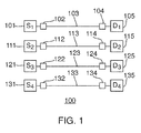
- a first embodiment of a thin-film optical sensing network 100 which consists of a number of straight optical pathways 103, 113, 123, 133 formed or positioned in an array in a thin flexible deformable material such as a suitable plastic.
- Each pathway 103, 113, 123, 133 may be a waveguide or equivalent formed in the plastic material or separate optical fibers positioned within the plastic material.
- Each optical pathway 103, 113, 123, 133 is coupled to an associated respective light source S 1 101, S 2 111, S 3 121, S 4 131 via input optics 102, 112, 122, 132 at a first end of the associated optical pathway 103, 113, 123, 133.
- each optical pathway 103, 113, 123, 133 is coupled to an associated respective detector D 1 105, D 2 115, D 3 125, D 4 135 via associated respective output optics 104, 114, 124, 134 at a second end of the associated optical pathway 103, 113, 123, 133.
- Each optical pathway 103, 113, 123, 133 acts as an optical strain gauge and, when the thin-film optical sensing network 100 is subjected to pressure stresses, the signals received by one or more of the detectors D 1 105, D 2 115, D 3 125, D 4 135 will reflect such pressure stresses.
- FIG. 1 shows four parallel optical pathways 103, 113, 123, 133, for all of the embodiments shown herein, the number of optical pathways included and the layout of each optical pathway may vary depending on the desired size and resolution of the sensing network.
- each light source S 1 101, S 2 111, S 3 121, S 4 131 provides a predetermined light signal that passes through the associated respective optical pathway 103, 113, 123, 133 and ultimately to the associated respective detector D 1 105, D 2 115, D 3 125, D 4 135.
- the respective outputs of each of the detectors D 1 105, D 2 115, D 3 125, D 4 135 are then provided to a processor 108 (not shown in Fig. 1 ) for appropriate processing and analysis (discussed below in further detail with respect to FIG. 6 ) to determine an amount and a location of any pressure being applied to thin-film optical sensing network 100.
- the thin-film optical sensing network 100 shown in FIG. 1 is much more sensitive and much more compact than conventional tactile sensors based on strain-gauge technology.
- a second embodiment of a thin-film optical sensing network 200 which consists of a number of curved optical pathways 203, 213, 223, 233 that are, as with the FIG. 1 embodiment, formed or positioned in an array in a thin flexible deformable material such as a suitable plastic and may be either separate waveguides or the equivalent formed in the plastic material or separate optical fibers positioned within the plastic material.
- Each optical pathway 203, 213, 223, 233 is coupled to an associated respective light source S 1 201, S 2 211, S 3 221, S 4 231 via input optics 202, 212, 222, 232 at a first end of the associated optical pathway 203, 213, 223, 233.
- each optical pathway 203, 213, 223, 233 is coupled to an associated respective detector D 1 205, D 2 215, D 3 225, D 4 235 via associated respective output optics 204, 214, 224, 234 at a second end of the associated optical pathway 203, 213, 223, 233.
- Each optical pathway 203, 213, 223, 233 acts as an optical strain gauge and, when the thin-film optical sensing network 200 is subjected to pressure stresses, the signals received by one or more of the detectors D 1 205, D 2 215, D 3 225, D 4 235 will reflect such pressure stresses.
- each light source S 1 201, S 2 211, S 3 221, S 4 231 provides a predetermined light signal that passes through the associated respective optical pathway 203, 213, 223, 233 and ultimately to the associated respective detector D 1 205, D 2 215, D 3 225, D 4 235.
- the respective outputs of each of the detectors D 1 205, D 2 215, D 3 225, D 4 235 are then provided to a processor for appropriate processing and analysis to determine an amount and a location of any pressure being applied to thin-film optical sensing network 200.
- a third embodiment of a thin-film optical sensing network 300 which consists of a number of optical pathways 303, 313, 323, 333, 343, 353, 363, 373 formed or positioned in an array in a thin flexible deformable material such as a suitable plastic, and may be either separate waveguides or the equivalent formed in the plastic material or separate optical fibers positioned within the plastic material.
- optical pathways 303, 313, 323, 333 are positioned in a first direction and optical pathways 343, 353, 363, 373 are positioned in a second direction perpendicular to the first direction.
- Optical pathways 303, 313, 323, 333, 343, 353, 363, 373 thus form a two-dimensional Cartesian grid.
- Each optical pathway 303, 313, 323, 333, 343, 353, 363, 373 may be straight as shown in FIG. 1 above or curved as shown in FIG. 2 above.
- Each optical pathway 303, 313, 323, 333, 343, 353, 363, 373 is coupled to an associated respective light source S 1 301, S 2 311, S 3 321, S 4 331, S 5 341, S 6 351, S 7 361, S 8 371 via input optics (not shown in FIG. 3 ) at a first end of the associated optical pathway 303, 313, 323, 333, 343, 353, 363, 373.
- each optical pathway 303, 313, 323, 333, 343, 353, 363, 373 is coupled to an associated respective detector D 1 305, D 2 315, D 3 325, D 4 335, D 5 345, D 6 355, D 7 365, D 8 375 via associated respective output optics (not shown in FIG. 3 ) at a second end of the associated optical pathway 303, 313, 323, 333, 343, 353, 363, 373.
- Each optical pathway 303, 313, 323, 333, 343, 353, 363, 373 acts as an optical strain gauge and, when the thin-film optical sensing network 300 is subjected to pressure stresses, the signals received by one or more of the detectors D 1 305, D 2 315, D 3 325, D 4 335, D 5 345, D 6 355, D 7 365, D 8 375 will reflect such pressure stresses.
- the dotted points e.g., points 380, 381, 382 are included to show that the optical pathways are interconnected at such points (reference numbers are not included for each point for clarity in FIG. 3 ) to allow light from one optical pathway to be directed into another adjacent optical pathway, allowing for better sensitivity to the stress or strain induced in the plastic material.
- each light source S 1 301, S 2 311, S 3 321, S 4 331, S 5 341, S 6 351, S 7 361, S 8 371 provides a predetermined light signal that passes through the associated respective optical pathway 303, 313, 323, 333, 343, 353, 363, 373 and ultimately to the associated respective detector D 1 305, D 2 315, D 3 325, D 4 335, D 5 345, D 6 355, D 7 365, D 8 375.
- the respective outputs of each of the detectors D 1 305, D 2 315, D 3 325, D 4 335, D 5 345, D 6 355, D 7 365, D 8 375 are then provided to a processor for appropriate processing and analysis (discussed below in further detail with respect to FIG. 6 ) to determine an amount and a location of any pressure being applied to thin-film optical sensing network 300.
- a fourth embodiment of a thin-film optical sensing network 400 which consists of a number of optical pathways 403, 413, 423, 433, 443, 453, 463, 473 formed or positioned in an array in a thin flexible deformable material such as a suitable plastic, and may be either separate waveguides or the equivalent formed in the plastic material or separate optical fibers positioned within the plastic material.
- This embodiment is similar to the FIG.
- optical pathways 403, 413, 423, 433, 443, 453, 463, 473 are not interconnected at the crossing points such no light is ever diverted from one of the optical pathways 403, 413, 423, 433, 443, 453, 463, 473 to another of the optical pathways 403, 413, 423, 433, 443, 453, 463, 473.
- optical pathways 403, 413, 423, 433, 443, 453, 463, 473 form a two-dimensional Cartesian grid.
- Each optical pathway 403, 413, 423, 433, 443, 453, 463, 473 may be straight as shown in FIG. 1 above or curved as shown in FIG. 2 above.
- Each optical pathway 403, 413, 423, 433, 443, 453, 463, 473 is coupled to an associated respective light source S 1 401, S 2 411, S 3 421, S 4 431, S 5 441, S 6 451, S 7 461, S 8 471 via input optics (not shown in FIG. 4 ) at a first end of the associated optical pathway 403, 413, 423, 433, 443, 453, 463, 473.
- each optical pathway 3403, 413, 423, 433, 443, 453, 463, 473 is coupled to an associated respective detector D 1 405, D 2 415, D 3 425, D 4 435, D 5 445, D 6 455, D 7 465, D 8 475 via associated respective output optics (not shown in FIG.
- Each optical pathway 403, 413, 423, 433, 443, 453, 463, 473 acts as an optical strain gauge and, when the thin-film optical sensing network 400 is subjected to pressure stresses, the signals received by one or more of the detectors D 1 405, D 2 415, D 3 425, D 4 435, D 5 445, D 6 455, D 7 465, D 8 475 will reflect such pressure stresses.
- each light source S 1 401, S 2 411, S 3 421, S 4 431, S 5 441, S 6 451, S 7 461, S 8 471 provides a predetermined light signal that passes through the associated respective optical pathway 403, 413, 423, 433, 443, 453, 463, 473 and ultimately to the associated respective detector D 1 405, D 2 415, D 3 425, D 4 435, D 5 445, D 6 455, D 7 465, D 8 475.
- the respective outputs of each of the detectors D 1 405, D 2 415, D 3 425, D 4 435, D 5 445, D 6 455, D 7 465, D 8 475 are then provided to a processor for appropriate processing and analysis (discussed below in further detail with respect to FIG. 6 ) to determine an amount and a location of any pressure being applied to thin-film optical sensing network 400.
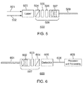
- a laser light source 503 includes an electrical input 501 coupled to a power source and a control input 502.
- the control input 502 may be coupled to a processor such as processor 608 shown in FIG. 6 or to a separate control processor (not shown).
- the laser light source 503 may be a diode laser or a solid state laser.
- the output of the laser light source 503 is directed through the input optics 508 and then onto an optical pathway 509.
- the input optics preferably include a polarizer 504, a polarization rotator 505, a wavelength selector 506 and optical pathway injection optics 507.
- the polarizer 504 may be a solid state device or be film-based.
- the polarization rotator 505 is optional and rotates the polarization axis of the linearly polarized light beam from the laser light source 503/polarizer 504 by an angle of choice.
- the wavelength selector 506 acts as a notch filter to pass only the desired wavelength of light from laser light source 503.
- the optical pathway injection optics 507 are lenses that focus the beam of light from laser light source 503 onto the optical pathway 509. In some cases, as discussed below, two separate light sources may be used to excite each optical pathway. In such cases, an optical coupler may be used to combine the output of each light source (after such output passes though the output optics) onto the optical fiber.
- an optical pathway 601 is shown coupled to the output optics 607 consisting of capture optics 602, a wavelength selector 603, and a polarization selector 604, which in turn is coupled to a light detector 605 having an output coupled to a processor 608 via a link 606.
- the capture optics 602 are lenses that collect the light from optical pathway 601 and direct such light towards detector 605 through the remaining portions of output optics 607.
- the wavelength selector 603 is selected to pass only the wavelength of interest in the light received from optical pathway 601.
- the polarization selector 604 ensures that the appropriate level of polarization is provided to detector 605.
- the detector 605 is a conventional light detector that generates an electrical output signal on link 606 proportional to the amount of light received.
- the processor 608 receives the electrical signals from each detector 604 in the thin-film optical sensing network (although only one detector 604 is shown in FIG. 6 , all of the embodiments of a thin-film optical sensing network disclosed herein include a plurality of detectors, each coupled to the processor for processing) and generates an output signal proportional to the amount of pressor applied to that network.
- processor 608 may also generate a separate signal indicating, in a two-dimensional plane, where such pressure is applied within the thin-film optical sensing network.
- the induced pressure causes localized changes in the microscopic nonlinearities of the embedded optical pathways.
- the material forming such optical pathways moves out of its equilibrium state, increasing local nonlinearities.
- the pressure sensing systems disclosed herein takes advantage of this change which causes changes to the nonlinear optical properties of the materials forming the optical pathways.
- the disclosed systems provide a much higher signal-to-noise response than previous linear systems.
- each optical pathway When a single light signal is applied to each optical pathway, such light signal will have a predetermined wavelength and polarization. When two light signals are applied to each optical pathway, each of the light signals will have a predetermined wavelength and polarization.
- the responsive signal monitored at the output end of each optical pathway in both cases will have a different predetermined wavelength and polarization that have magnitudes that change as pressure is applied to the optical pathway.
- the output signals generated can be based on a change in magnitude of the received signal at the particular wavelength and/or based on a change in the polarization of such signal at that wavelength.
- the predetermined wavelength and/or polarization monitored at the output of each optical pathway can be selected based on a number of different cases, including, for example, second harmonic generation (output will have twice the wavelength of the input wavelength) and Raman Scattering (output selected based on Raman Stokes or Anti-Stokes peaks).
- the predetermined wavelength and/or polarization monitored at the output of each optical pathway can be selected based on, for example, sum-frequency generation (output wavelength at the sum of the two input wavelengths), difference-frequency generation (output wavelength at difference of two input wavelengths), and simulated Raman Scattering (output wavelength at twice one of the input wavelengths less the other input wavelengths).
- the thin-film sensing networks disclosed herein avoid the various problems that arise due to permanent deformation in conventional electro-mechanical pressure sensors.
- each of optical pathways causes variations in the magnitude of light transmitted there through to the second end when pressure is applied to an optical pathway in a region in the array of optical pathways, or to a region in the array of optical pathways.
- the processor determines the amount of pressure applied to the region of the array of optical pathways based at least on changes in the output signals from the one or more light detectors (e.g., a change in magnitude of light at the second predetermined frequency) coupled to the one or more optical pathways to which a pressure was applied.
Landscapes
- Physics & Mathematics (AREA)
- General Physics & Mathematics (AREA)
- Engineering & Computer Science (AREA)
- Chemical & Material Sciences (AREA)
- Analytical Chemistry (AREA)
- General Engineering & Computer Science (AREA)
- Theoretical Computer Science (AREA)
- Force Measurement Appropriate To Specific Purposes (AREA)
- Human Computer Interaction (AREA)
- Optics & Photonics (AREA)
- Measuring Fluid Pressure (AREA)
Abstract
Description
- This disclosure relates generally to a system and method for tactile sensing using thin film optical sensing networks.
- Many areas exist where it is beneficial to implement an artificial sense of touch. A tactile sensor is a transducer that can be used to provide this artificial sense of touch by measuring the force applied between a surface of the transducer and an object in contact with the transducer surface. Tactile sensors are commonly used in applications which involve handling or manipulation of an object (e.g., robotic grippers) to ensure that the amount of force applied to such object remains well below a level that might cause damage to the object but with enough force to adequately grip and control the object. Tactile sensors formed from pressure sensor arrays, strain gauge rosettes, or other electro-mechanical sensing systems are subject to permanent deformation when subjected to repetitive stresses during operation, providing shifting sensitivity, less than optimal reliability and a short life span.
- Accordingly, there is a need for an improved system and method for tactile sensing which overcomes the problems recited above.
- In one aspect, a thin-film flexible tactile sensor includes a sensing network formed from an array of optical pathways arranged in a flexible material. Each of the optical pathways has an input at a first end thereof and an output at a second end thereof. The thin-film flexible tactile sensor also includes a plurality of light sources, one for each of the optical pathways. Each of the plurality of light sources is coupled to the input of a respective associated optical pathway. Each of the plurality of light sources directs a light signal having a first predetermined frequency and characteristic into the associated optical pathway. The thin-film flexible tactile sensor further includes a plurality of light detectors, one for each of the optical pathways. Each of the plurality of light detectors is coupled to the output of a respective associated optical pathway. Each of the plurality of light detectors receives a light signal from the associated optical pathway and generates an output signal corresponding to the magnitude of the received light signal at a second predetermined frequency. The thin-film flexible tactile sensor still further includes a processor coupled to receive the output signals from each of the plurality of light detectors. The processor is configured to determine an amount of pressure applied to the sensing network based on the received signals from the plurality of light detectors.
- In another aspect, a thin-film flexible tactile sensor includes a sensing network formed from an array of one or more optical pathways arranged in a flexible material. Each of the optical pathways has an input at a first end thereof and an output at a second end thereof. The film flexible tactile sensor also includes one or more light sources, one for each of the optical pathways. Each of the one or more light sources is coupled to the input of a respective associated optical pathway. Each of the one or more light sources directs a light signal having a first predetermined frequency and characteristic into the associated optical pathway. The film flexible tactile sensor further includes one or more light detectors, one for each of the optical pathways. Each of the one or more light detectors is coupled to the output of a respective associated optical pathway. Each of the one or more light detectors receives a light signal from the associated optical pathway and generates an output signal corresponding to the magnitude of the received light signal at a second predetermined frequency. The film flexible tactile sensor still further includes a processor coupled to receive the output signals from each of the one or more light detectors. The processor is configured to determine an amount of pressure applied to the sensing network based on the received signals from the one or more light detectors.
- In yet another aspect, a method for sensing pressure uses a sensing network formed from an array of optical pathways arranged in a flexible material. Each of the optical pathways has an input at a first end thereof and an output at a second end thereof. Light signals are directed into each of the optical pathways. Each of the light signals has a first predetermined frequency and characteristic. A light signal is received at the output of each of the optical pathways and output signals are generated corresponding to the magnitude of each received light signal at a second predetermined frequency at the output of the associated optical pathway. The output signals are processed to determine an amount of pressure applied to the sensing network.
- The features, functions, and advantages that have been discussed can be achieved independently in various embodiments or may be combined in yet other embodiments, further details of which can be seen with reference to the following description and drawings.
- The following detailed description, given by way of example and not intended to limit the present disclosure solely thereto, will best be understood in conjunction with the accompanying drawings in which:
-
FIG. 1 is a block diagram illustrating an embodiment of a thin-film optical sensing network according to an aspect of the disclosure; -
FIG. 2 is a block diagram illustrating a second embodiment of a thin-film optical sensing network according to an aspect of the disclosure; -
FIG. 3 is a block diagram illustrating a third embodiment of a thin-film optical sensing network according to an aspect of the disclosure; -
FIG. 4 is a block diagram illustrating a fourth embodiment of a thin-film optical sensing network according to an aspect of the disclosure; -
FIG. 5 is a block diagram illustrating an optical light source and input optics for use with the thin-film optical sensing networks of the present disclosure; and -
FIG. 6 is a block diagram illustrating the output optics and detector for use with the thin-film optical sensing networks of the present disclosure. - In the present disclosure, like reference numbers refer to like elements throughout the drawings, which illustrate various exemplary embodiments of the present disclosure.
- Referring now to
FIG. 1 , a first embodiment of a thin-filmoptical sensing network 100 is shown which consists of a number of straightoptical pathways pathway optical pathway light source S 1 101,S 2 111, S3 121,S 4 131 viainput optics optical pathway optical pathway respective detector D 1 105,D 2 115,D 3 125,D 4 135 via associatedrespective output optics optical pathway optical pathway optical sensing network 100 is subjected to pressure stresses, the signals received by one or more of thedetectors D 1 105,D 2 115,D 3 125,D 4 135 will reflect such pressure stresses. Although the embodiment shown inFIG. 1 shows four paralleloptical pathways - In operation, each
light source S 1 101,S 2 111, S3 121,S 4 131 provides a predetermined light signal that passes through the associated respectiveoptical pathway respective detector D 1 105,D 2 115,D 3 125,D 4 135. The respective outputs of each of thedetectors D 1 105,D 2 115,D 3 125,D 4 135 are then provided to a processor 108 (not shown inFig. 1 ) for appropriate processing and analysis (discussed below in further detail with respect toFIG. 6 ) to determine an amount and a location of any pressure being applied to thin-filmoptical sensing network 100. The thin-filmoptical sensing network 100 shown inFIG. 1 is much more sensitive and much more compact than conventional tactile sensors based on strain-gauge technology. - Referring now to
FIG. 2 , a second embodiment of a thin-filmoptical sensing network 200 is shown which consists of a number of curvedoptical pathways FIG. 1 embodiment, formed or positioned in an array in a thin flexible deformable material such as a suitable plastic and may be either separate waveguides or the equivalent formed in the plastic material or separate optical fibers positioned within the plastic material. Eachoptical pathway light source S 1 201,S 2 211,S 3 221, S4 231 viainput optics optical pathway optical pathway respective detector D 1 205, D2 215,D 3 225,D 4 235 via associatedrespective output optics optical pathway optical pathway optical sensing network 200 is subjected to pressure stresses, the signals received by one or more of thedetectors D 1 205, D2 215,D 3 225,D 4 235 will reflect such pressure stresses. - In operation, each
light source S 1 201,S 2 211,S 3 221, S4 231 provides a predetermined light signal that passes through the associated respectiveoptical pathway respective detector D 1 205, D2 215,D 3 225,D 4 235. As with theFIG. 1 embodiment, the respective outputs of each of thedetectors D 1 205, D2 215,D 3 225,D 4 235 are then provided to a processor for appropriate processing and analysis to determine an amount and a location of any pressure being applied to thin-filmoptical sensing network 200. - Referring now to
FIG. 3 , a third embodiment of a thin-filmoptical sensing network 300 is shown which consists of a number ofoptical pathways FIG. 3 ,optical pathways optical pathways Optical pathways optical pathway FIG. 1 above or curved as shown inFIG. 2 above. Eachoptical pathway light source S 1 301,S 2 311,S 3 321,S 4 331,S 5 341,S 6 351,S 7 361,S 8 371 via input optics (not shown inFIG. 3 ) at a first end of the associatedoptical pathway optical pathway respective detector D 1 305,D 2 315,D 3 325,D 4 335,D 5 345,D 6 355,D 7 365,D 8 375 via associated respective output optics (not shown inFIG. 3 ) at a second end of the associatedoptical pathway optical pathway optical sensing network 300 is subjected to pressure stresses, the signals received by one or more of thedetectors D 1 305,D 2 315,D 3 325,D 4 335,D 5 345,D 6 355,D 7 365,D 8 375 will reflect such pressure stresses. The dotted points (e.g., points 380, 381, 382) are included to show that the optical pathways are interconnected at such points (reference numbers are not included for each point for clarity inFIG. 3 ) to allow light from one optical pathway to be directed into another adjacent optical pathway, allowing for better sensitivity to the stress or strain induced in the plastic material. - In operation, each
light source S 1 301,S 2 311,S 3 321,S 4 331,S 5 341,S 6 351,S 7 361,S 8 371 provides a predetermined light signal that passes through the associated respectiveoptical pathway respective detector D 1 305,D 2 315,D 3 325,D 4 335,D 5 345,D 6 355,D 7 365,D 8 375. The respective outputs of each of thedetectors D 1 305,D 2 315,D 3 325,D 4 335,D 5 345,D 6 355,D 7 365,D 8 375 are then provided to a processor for appropriate processing and analysis (discussed below in further detail with respect toFIG. 6 ) to determine an amount and a location of any pressure being applied to thin-filmoptical sensing network 300. - Referring now to
FIG. 4 , a fourth embodiment of a thin-filmoptical sensing network 400 is shown which consists of a number ofoptical pathways FIG. 3 embodiment, except theoptical pathways optical pathways optical pathways FIG. 3 embodiment,optical pathways optical pathway FIG. 1 above or curved as shown inFIG. 2 above. Eachoptical pathway light source S 1 401,S 2 411,S 3 421,S 4 431,S 5 441,S 6 451,S 7 461,S 8 471 via input optics (not shown inFIG. 4 ) at a first end of the associatedoptical pathway optical pathway respective detector D 1 405,D 2 415,D 3 425,D 4 435,D 5 445,D 6 455,D 7 465,D 8 475 via associated respective output optics (not shown inFIG. 3 ) at a second end of the associatedoptical pathway optical pathway optical sensing network 400 is subjected to pressure stresses, the signals received by one or more of thedetectors D 1 405,D 2 415,D 3 425,D 4 435,D 5 445,D 6 455,D 7 465,D 8 475 will reflect such pressure stresses. - In operation, each
light source S 1 401,S 2 411,S 3 421,S 4 431,S 5 441,S 6 451,S 7 461,S 8 471 provides a predetermined light signal that passes through the associated respectiveoptical pathway respective detector D 1 405,D 2 415,D 3 425,D 4 435,D 5 445,D 6 455,D 7 465,D 8 475. The respective outputs of each of thedetectors D 1 405,D 2 415,D 3 425,D 4 435,D 5 445,D 6 455,D 7 465,D 8 475 are then provided to a processor for appropriate processing and analysis (discussed below in further detail with respect toFIG. 6 ) to determine an amount and a location of any pressure being applied to thin-filmoptical sensing network 400. - Referring now to
FIG. 5 , the light source and input optics coupled to each optical pathway in the embodiments shown inFIGS. 1 to 4 are show in greater detail. In particular alaser light source 503 includes anelectrical input 501 coupled to a power source and acontrol input 502. Thecontrol input 502 may be coupled to a processor such asprocessor 608 shown inFIG. 6 or to a separate control processor (not shown). Thelaser light source 503 may be a diode laser or a solid state laser. The output of thelaser light source 503 is directed through theinput optics 508 and then onto anoptical pathway 509. The input optics preferably include apolarizer 504, apolarization rotator 505, awavelength selector 506 and opticalpathway injection optics 507. Thepolarizer 504 may be a solid state device or be film-based. Thepolarization rotator 505 is optional and rotates the polarization axis of the linearly polarized light beam from thelaser light source 503/polarizer 504 by an angle of choice. Thewavelength selector 506 acts as a notch filter to pass only the desired wavelength of light fromlaser light source 503. The opticalpathway injection optics 507 are lenses that focus the beam of light fromlaser light source 503 onto theoptical pathway 509. In some cases, as discussed below, two separate light sources may be used to excite each optical pathway. In such cases, an optical coupler may be used to combine the output of each light source (after such output passes though the output optics) onto the optical fiber. - Referring now to
FIG. 6 , the output optics and light detector coupled to each optical pathway in the embodiments shown inFIGS. 1 to 4 are shown in greater detail, along with the processor used to generate an output signal based on pressure applied to the respective embodiments of the thin-film optical sensing network shown inFIGS. 1 to 4 . In particular, anoptical pathway 601 is shown coupled to theoutput optics 607 consisting ofcapture optics 602, awavelength selector 603, and apolarization selector 604, which in turn is coupled to alight detector 605 having an output coupled to aprocessor 608 via alink 606. Thecapture optics 602 are lenses that collect the light fromoptical pathway 601 and direct such light towardsdetector 605 through the remaining portions ofoutput optics 607. Thewavelength selector 603 is selected to pass only the wavelength of interest in the light received fromoptical pathway 601. Thepolarization selector 604 ensures that the appropriate level of polarization is provided todetector 605. Thedetector 605 is a conventional light detector that generates an electrical output signal onlink 606 proportional to the amount of light received. Theprocessor 608 receives the electrical signals from eachdetector 604 in the thin-film optical sensing network (although only onedetector 604 is shown inFIG. 6 , all of the embodiments of a thin-film optical sensing network disclosed herein include a plurality of detectors, each coupled to the processor for processing) and generates an output signal proportional to the amount of pressor applied to that network. In addition,processor 608 may also generate a separate signal indicating, in a two-dimensional plane, where such pressure is applied within the thin-film optical sensing network. - When pressure is applied to any of the disclosed embodiments of a thin-film optical sensing network, the induced pressure causes localized changes in the microscopic nonlinearities of the embedded optical pathways. In particular, by inducing stress in the optical pathways, the material forming such optical pathways moves out of its equilibrium state, increasing local nonlinearities. The pressure sensing systems disclosed herein takes advantage of this change which causes changes to the nonlinear optical properties of the materials forming the optical pathways. In particular, by applying a light signal having a particular characteristic to each optical pathway, and monitoring a responsive (but non-linear) characteristic, the disclosed systems provide a much higher signal-to-noise response than previous linear systems.
- When a single light signal is applied to each optical pathway, such light signal will have a predetermined wavelength and polarization. When two light signals are applied to each optical pathway, each of the light signals will have a predetermined wavelength and polarization. To take advantage of the non-linear optical properties of the materials forming the optical pathways, the responsive signal monitored at the output end of each optical pathway in both cases (single light signals and two light signals) will have a different predetermined wavelength and polarization that have magnitudes that change as pressure is applied to the optical pathway. As such, the output signals generated can be based on a change in magnitude of the received signal at the particular wavelength and/or based on a change in the polarization of such signal at that wavelength. When a single light signal is applied to each optical pathway, the predetermined wavelength and/or polarization monitored at the output of each optical pathway can be selected based on a number of different cases, including, for example, second harmonic generation (output will have twice the wavelength of the input wavelength) and Raman Scattering (output selected based on Raman Stokes or Anti-Stokes peaks). When two light signals are applied to each optical pathway, the predetermined wavelength and/or polarization monitored at the output of each optical pathway can be selected based on, for example, sum-frequency generation (output wavelength at the sum of the two input wavelengths), difference-frequency generation (output wavelength at difference of two input wavelengths), and simulated Raman Scattering (output wavelength at twice one of the input wavelengths less the other input wavelengths).
- By using optical pathways formed in a deformable material such as a plastic or optical fibers positioned within such a deformable material, the thin-film sensing networks disclosed herein avoid the various problems that arise due to permanent deformation in conventional electro-mechanical pressure sensors.
- In operation, each of optical pathways causes variations in the magnitude of light transmitted there through to the second end when pressure is applied to an optical pathway in a region in the array of optical pathways, or to a region in the array of optical pathways. The processor determines the amount of pressure applied to the region of the array of optical pathways based at least on changes in the output signals from the one or more light detectors (e.g., a change in magnitude of light at the second predetermined frequency) coupled to the one or more optical pathways to which a pressure was applied.
- Further, the disclosure comprises embodiments according to the following clauses:
- Clause 1. A thin-film flexible tactile sensor, comprising:
- a sensing network formed from an array of optical pathways arranged in a flexible material, each of the optical pathways having an input at a first end thereof and an output at a second end thereof;
- a plurality of light sources, one for each of the optical pathways, each of the plurality of light sources coupled to the input of a respective associated optical pathway, each of the plurality of light sources directing a light signal having a first predetermined frequency and characteristic into the associated optical pathway;
- a plurality of light detectors, one for each of the optical pathways, each of the plurality of light detectors coupled to the output of a respective associated optical pathway, each of the plurality of light detectors receiving a light signal from the associated optical pathway and generating an output signal corresponding to the magnitude of the received light signal at a second predetermined frequency; and
- a processor coupled to receive the output signals from each of the plurality of light detectors and configured to determine an amount of pressure applied to the sensing network based on the received signals from the plurality of light detectors.
- Clause 2. The thin-film flexible tactile sensor of Clause 1, wherein the processor is further configured to determine a location within the tactile sensor of the amount of pressure applied to the sensing network based on the received signals from the plurality of light detectors.
- Clause 3. The thin-film flexible tactile sensor of Clause 1, further comprising input optics coupled between each of the plurality of light sources and the input of the associated optical pathway.
- Clause 4. The thin-film flexible tactile sensor of Clause 3, wherein the input optics comprise at least one of a polarizer, a polarization rotator and a wavelength selector.
- Clause 5. The thin-film flexible tactile sensor of Clause 1, further comprising output optics coupled between each of the plurality of light detectors and the output of the associated optical pathway.
- Clause 6. The thin-film flexible tactile sensor of Clause 5, wherein the output optics comprise at least one of a wavelength selector and a polarization selector.
- Clause 7. The thin-film flexible tactile sensor of Clause 1, wherein each of optical pathways causes variations in the magnitude of light transmitted there through to the second end when pressure is applied to an optical pathway in a region in the array, and wherein the processor is configured to determine the amount of pressure applied to the region of the array of optical pathways based at least on changes in the output signals from the one or more light detectors coupled to the one or more optical pathways to which a pressure was applied.
- 8. The thin-film flexible tactile sensor of Clause 1, wherein each of optical pathways causes variations in the magnitude of light transmitted there through to the second end when pressure is applied to a region of the array of optical pathways, and wherein the processor is configured to determine the amount of pressure applied to the region of the array of optical pathways based at least on changes in the output signals from the one or more light detectors coupled to the one or more optical pathways to which a pressure was applied.
- Clause 9. The thin-film flexible tactile sensor of Clause 1, wherein each of optical pathways causes variations in the magnitude of the light transmitted there through to the second end when pressure is applied to an optical pathway in a region in the array, and wherein the processor is configured to determine the amount of pressure applied to the region of the array of optical pathways based at least on changes in the output signals from the one or more light detectors reflective of a change in magnitude of light at the second predetermined frequency transmitted to the second end of the pne or more optical pathways to which a pressure was applied
- Clause 10. The thin-film flexible tactile sensor of Clause 1, wherein the second predetermined frequency is twice the first predetermined frequency.
- Clause 11. The thin-film flexible tactile sensor of Clause 1, wherein the second predetermined frequency corresponds to Raman Stokes Outputs or Raman Anti-Stokes Outputs of the first predetermined frequency.
- Clause 12. The thin-film flexible tactile sensor of Clause 1, further comprising:
- a plurality of second light sources, one for each of the optical pathways, each of the plurality of second light sources coupled to the input of a respective associated optical pathway, each of the plurality of second light sources directing a light signal having a third predetermined frequency and characteristic into the associated optical pathway; and
- wherein the second predetermined frequency is determined based on a function of the first predetermined frequency and the third predetermined frequency.
- 13. The thin-film flexible tactile sensor of Clause 12, wherein the function corresponds to a sum-frequency function.
- 14. The thin-film flexible tactile sensor of Clause 12, wherein the function corresponds to a difference-frequency function
- 15. The thin-film flexible tactile sensor of Clause 12, wherein the function corresponds to a simulated Raman Scattering function.
- 16. The thin-film flexible tactile sensor of Clause 1, wherein the optical pathways form a two-dimensional Cartesian grid and wherein the optical pathways are connected at each crossing point within the two-dimensional Cartesian grid.
- 17. The thin-film flexible tactile sensor of Clause 1, wherein each of the optical pathways is formed within the flexible material.
- 18. The thin-film flexible tactile sensor of Clause 1, wherein each of the optical pathways is a separate optical fiber positioned within the flexible material.
- 19. A thin-film flexible tactile sensor, comprising:
- a sensing network formed from an array of one or more optical pathways arranged in a flexible material, each of the optical pathways having an input at a first end thereof and an output at a second end thereof;
- one or more light sources, one for each of the optical pathways, each of the one or more light sources coupled to the input of a respective associated optical pathway, each of the one or more light sources directing a light signal having a first predetermined frequency and characteristic into the associated optical pathway;
- one or more light detectors, one for each of the optical pathways, each of the one or more light detectors coupled to the output of a respective associated optical pathway, each of the one or more light detectors receiving a light signal from the associated optical pathway and generating an output signal corresponding to the magnitude of the received light signal at a second predetermined frequency; and
- a processor coupled to receive the output signals from each of the one or more light detectors and configured to determine an amount of pressure applied to the sensing network based on the received signals from the one or more light detectors.
- 20. The thin-film flexible tactile sensor of Clause 19, wherein the processor is further configured to determine a location within the tactile sensor of the amount of pressure applied to the sensing network based on the received signals from the one or more light detectors.
- 21. The thin-film flexible tactile sensor of Clause 19, wherein each of optical pathways causes variations in the magnitude of the light transmitted there through to the second end when pressure is applied to an optical pathway in a region in the array, and wherein the processor is configured to determine the amount of pressure applied to the region of the array of optical pathways based at least on changes in the output signals from the one or more light detectors reflective of a change in magnitude of light at the second predetermined frequency transmitted to the second end of the one or more optical pathways to which a pressure was applied.
- 22. A method for sensing pressure using a sensing network formed from an array of optical pathways arranged in a flexible material, each of the optical pathways having an input at a first end thereof and an output at a second end thereof, comprising the steps of:
- directing light signals into each of the optical pathways, each of the light signals having a first predetermined frequency and characteristic;
- at the output of each of the optical pathways, receiving a light signal and generating an output signal corresponding to the magnitude of the received light signal at a second predetermined frequency at the output of the associated optical pathway; and
- processing the output signals to determine an amount of pressure applied to the sensing network.
- Clause 23. The method of Clause 22, further comprising the step of processing the output signals to determine a location within the sensing network of the amount of pressure applied to the sensing network.
- Although the present disclosure has been particularly shown and described with reference to the preferred embodiments and various aspects thereof, it will be appreciated by those of ordinary skill in the art that various changes and modifications may be made without departing from the spirit and scope of the disclosure. It is intended that the appended claims be interpreted as including the embodiments described herein, the alternatives mentioned above, and all equivalents thereto.
Claims (14)
- A thin-film flexible tactile sensor, comprising:a sensing network (100) formed from an array of optical pathways (103, 203, 303, 113, 213, 313, 123, 223, 323, 133, 233, 333) arranged in a flexible material, each of the optical pathways having an input at a first end thereof and an output at a second end thereof;a plurality of light sources (101, 201, 301, 111, 211, 311, 121, 221, 321, 131, 231, 331), one for each of the optical pathways (103, 203, 303, 113, 213, 313, 123, 223, 323, 133, 233, 333), each of the plurality of light sources coupled to the input of a respective associated optical pathway, each of the plurality of light sources directing a light signal having a first predetermined frequency and characteristic into the associated optical pathway;a plurality of light detectors ( 105, 205, 305, 115, 215, 315, 125, 225, 325, 135, 235, 335), one for each of the optical pathways (103, 203, 303, 113, 213, 313, 123, 223, 323, 133, 233, 333), each of the plurality of light detectors coupled to the output of a respective associated optical pathway, each of the plurality of light detectors receiving a light signal from the associated optical pathway and generating an output signal corresponding to the magnitude of the received light signal at a second predetermined frequency; anda processor coupled to receive the output signals from each of the plurality of light detectors and configured to determine an amount of pressure applied to the sensing network based on the received signals from the plurality of light detectors.
- The thin-film flexible tactile sensor of claim 1, wherein the processor is further configured to determine a location within the tactile sensor of the amount of pressure applied to the sensing network based on the received signals from the plurality of light detectors.
- The thin-film flexible tactile sensor of claim 1 or 2, further comprising input optics (102, 202, 112, 212, 122, 222, 132, 232) coupled between each of the plurality of light sources and the input of the associated optical pathway.
- The thin-film flexible tactile sensor of claims 1 to 3, wherein the input optics comprise at least one of a polarizer, a polarization rotator and a wavelength selector.
- The thin-film flexible tactile sensor of any one of claims 1 to 4, further comprising output optics (104, 204, 114, 214, 124, 224, 134, 234) coupled between each of the plurality of light detectors and the output of the associated optical pathway, wherein the output optics comprise at least one of a wavelength selector and a polarization selector.
- The thin-film flexible tactile sensor of any one of claims 1 to 5, wherein each of optical pathways causes variations in the magnitude of light transmitted there through to the second end when pressure is applied to an optical pathway in a region in the array, and wherein the processor is configured to determine the amount of pressure applied to the region of the array of optical pathways based at least on changes in the output signals from the one or more light detectors coupled to the one or more optical pathways to which a pressure was applied.
- The thin-film flexible tactile sensor of any one of claims 1 to 6, wherein each of optical pathways causes variations in the magnitude of light transmitted there through to the second end when pressure is applied to a region of the array of optical pathways, and wherein the processor is configured to determine the amount of pressure applied to the region of the array of optical pathways based at least on changes in the output signals from the one or more light detectors coupled to the one or more optical pathways to which a pressure was applied.
- The thin-film flexible tactile sensor of any one of claims 1 to 7, wherein each of optical pathways causes variations in the magnitude of the light transmitted there through to the second end when pressure is applied to an optical pathway in a region in the array, and wherein the processor is configured to determine the amount of pressure applied to the region of the array of optical pathways based at least on changes in the output signals from the one or more light detectors reflective of a change in magnitude of light at the second predetermined frequency transmitted to the second end of the one or more optical pathways to which a pressure was applied.
- The thin-film flexible tactile sensor of any one of claims 1 to 8, wherein the second predetermined frequency is twice the first predetermined frequency.
- The thin-film flexible tactile sensor of any one of claims 1 to 9, wherein the second predetermined frequency corresponds to Raman Stokes Outputs or Raman Anti-Stokes Outputs of the first predetermined frequency.
- The thin-film flexible tactile sensor of any one of claims 1 to 10, further comprising:a plurality of second light sources, one for each of the optical pathways, each of the plurality of second light sources coupled to the input of a respective associated optical pathway, each of the plurality of second light sources directing a light signal having a third predetermined frequency and characteristic into the associated optical pathway; andwherein the second predetermined frequency is determined based on a function of the first predetermined frequency and the third predetermined frequency.
- The thin-film flexible tactile sensor of any one of claims 1 to 11, wherein the optical pathways form a two-dimensional Cartesian grid and wherein the optical pathways are connected at each crossing point within the two-dimensional Cartesian grid.
- A method for sensing pressure using a sensing network (101) formed from an array of optical pathways (103, 203, 303, 113, 213, 313, 123, 223, 323, 133, 233, 333) arranged in a flexible material, each of the optical pathways having an input at a first end thereof and an output at a second end thereof, comprising the steps of:directing light signals from a plurality of light sources (101, 201, 301, 111, 211, 311, 121, 221, 321, 131, 231, 331) into each of the optical pathways, each of the light signals having a first predetermined frequency and characteristic;at the output of each of the optical pathways, receiving a light signal at a plurality of light detectors ( 105, 205, 305, 115, 215, 315, 125, 225, 325, 135, 235, 335) and generating an output signal corresponding to the magnitude of the received light signal at a second predetermined frequency at the output of the associated optical pathway; andprocessing the output signals to determine an amount of pressure applied to the sensing network.
- The method of claim 13, further comprising the step of processing the output signals to determine a location within the sensing network at which a predetermined amount of pressure was applied to the sensing network.
Applications Claiming Priority (1)
| Application Number | Priority Date | Filing Date | Title |
|---|---|---|---|
| US14/951,390 US9534969B1 (en) | 2015-11-24 | 2015-11-24 | System and method for tactile sensing using thin film optical sensing networks |
Publications (2)
| Publication Number | Publication Date |
|---|---|
| EP3173758A1 true EP3173758A1 (en) | 2017-05-31 |
| EP3173758B1 EP3173758B1 (en) | 2018-11-28 |
Family
ID=56550134
Family Applications (1)
| Application Number | Title | Priority Date | Filing Date |
|---|---|---|---|
| EP16181120.3A Not-in-force EP3173758B1 (en) | 2015-11-24 | 2016-07-25 | System and method for tactile sensing using thin film optical sensing networks |
Country Status (7)
| Country | Link |
|---|---|
| US (1) | US9534969B1 (en) |
| EP (1) | EP3173758B1 (en) |
| JP (1) | JP2017116531A (en) |
| KR (1) | KR102602323B1 (en) |
| CN (1) | CN106918414B (en) |
| SG (1) | SG10201609222SA (en) |
| TW (1) | TWI718166B (en) |
Families Citing this family (3)
| Publication number | Priority date | Publication date | Assignee | Title |
|---|---|---|---|---|
| WO2021253420A1 (en) * | 2020-06-19 | 2021-12-23 | 华为技术有限公司 | Touch sensing device, electronic device, earphones, and watch |
| CN114046809B (en) * | 2021-11-11 | 2024-04-26 | 广东省科学院半导体研究所 | Optical sensing device, sensing equipment and system |
| CN118129805B (en) * | 2024-05-06 | 2024-09-13 | 天津工业大学 | A polymer-based ring resonant cavity mesh sensor array multifunctional sensor |
Citations (5)
| Publication number | Priority date | Publication date | Assignee | Title |
|---|---|---|---|---|
| US4781056A (en) * | 1985-03-07 | 1988-11-01 | Sopha Praxis | Optical device for strain detection, method for the measurement of strain by means of the said device and their application to scales |
| WO1993004350A1 (en) * | 1991-08-25 | 1993-03-04 | Avco Corporation | Optical fiber strain transducer having a radius of curvature equal to or less than a critical radius of curvature |
| WO2006037181A1 (en) * | 2004-10-06 | 2006-04-13 | Rmit University | An optical signal processing device |
| EP2236346A2 (en) * | 2009-04-02 | 2010-10-06 | Grammer Ag | Recognition device and method for recognising the occupation of a seat |
| WO2015109144A1 (en) * | 2014-01-16 | 2015-07-23 | University Of Florida Research Foundation, Inc. | Method for determining stress using raman spectroscopy |
Family Cites Families (18)
| Publication number | Priority date | Publication date | Assignee | Title |
|---|---|---|---|---|
| GB1544483A (en) * | 1976-07-01 | 1979-04-19 | Standard Telephones Cables Ltd | Strain measurement using optical fibres |
| JPH03243839A (en) * | 1990-02-22 | 1991-10-30 | Toshiba Corp | Optical fiber sensor |
| JPH0472520A (en) * | 1990-07-13 | 1992-03-06 | Nagano Keiki Seisakusho Ltd | Optical sensor for physical amount |
| US5257086A (en) * | 1992-06-09 | 1993-10-26 | D.O.M. Associates Int'l | Optical spectrophotometer having a multi-element light source |
| US5979244A (en) * | 1998-03-04 | 1999-11-09 | Siemens Aktiengesellschaft | Method and apparatus for evaluating internal film stress at high lateral resolution |
| US6097870A (en) * | 1999-05-17 | 2000-08-01 | Lucent Technologies Inc. | Article utilizing optical waveguides with anomalous dispersion at vis-nir wavelenghts |
| DE60143321D1 (en) * | 2001-03-27 | 2010-12-02 | Council Scient Ind Res | |
| US20040208439A1 (en) * | 2002-04-05 | 2004-10-21 | Becs Technology, Inc. | Method and apparatus for self-aligning photonic interconnections |
| US20040247223A1 (en) * | 2003-06-04 | 2004-12-09 | Tietjen Byron W. | System and method for multiplexing optical sensor array signals |
| JP2005265434A (en) * | 2004-03-16 | 2005-09-29 | Tama Tlo Kk | Stereoscopic structure and shape measuring device |
| US6990260B2 (en) * | 2004-06-09 | 2006-01-24 | Lockheed Martin Corporation | Extended intensity-based optical sensor |
| JP4938431B2 (en) * | 2006-12-12 | 2012-05-23 | 日本電信電話株式会社 | Optical fiber temperature / strain measurement method |
| ITPI20070085A1 (en) * | 2007-07-23 | 2009-01-24 | Scuola Superiore Di Studi Univ | FLEXIBLE TACTILE SENSOR AND METHOD TO OBTAIN IT |
| US20120325001A1 (en) * | 2011-06-27 | 2012-12-27 | The Boeing Company | Optical sensor systems and methods |
| US9170172B2 (en) * | 2011-08-23 | 2015-10-27 | The Boeing Company | Composite structure having an embedded sensing system |
| CN102564643A (en) * | 2012-02-28 | 2012-07-11 | 西南交通大学 | Method for automatic calibration and variable separation sensing for quasi-distributed fiber grating sensing network and device thereof |
| US9554484B2 (en) | 2012-03-30 | 2017-01-24 | The Board Of Trustees Of The University Of Illinois | Appendage mountable electronic devices conformable to surfaces |
| US9068925B1 (en) | 2012-06-27 | 2015-06-30 | The Boeing Company | Optical internal configuration monitoring system monitoring the bending of a platform for correcting travel direction of a platform |
-
2015
- 2015-11-24 US US14/951,390 patent/US9534969B1/en not_active Expired - Fee Related
-
2016
- 2016-07-21 TW TW105123036A patent/TWI718166B/en not_active IP Right Cessation
- 2016-07-25 EP EP16181120.3A patent/EP3173758B1/en not_active Not-in-force
- 2016-08-19 KR KR1020160105168A patent/KR102602323B1/en active Active
- 2016-10-19 CN CN201610911328.8A patent/CN106918414B/en not_active Expired - Fee Related
- 2016-11-03 SG SG10201609222SA patent/SG10201609222SA/en unknown
- 2016-11-17 JP JP2016223764A patent/JP2017116531A/en active Pending
Patent Citations (5)
| Publication number | Priority date | Publication date | Assignee | Title |
|---|---|---|---|---|
| US4781056A (en) * | 1985-03-07 | 1988-11-01 | Sopha Praxis | Optical device for strain detection, method for the measurement of strain by means of the said device and their application to scales |
| WO1993004350A1 (en) * | 1991-08-25 | 1993-03-04 | Avco Corporation | Optical fiber strain transducer having a radius of curvature equal to or less than a critical radius of curvature |
| WO2006037181A1 (en) * | 2004-10-06 | 2006-04-13 | Rmit University | An optical signal processing device |
| EP2236346A2 (en) * | 2009-04-02 | 2010-10-06 | Grammer Ag | Recognition device and method for recognising the occupation of a seat |
| WO2015109144A1 (en) * | 2014-01-16 | 2015-07-23 | University Of Florida Research Foundation, Inc. | Method for determining stress using raman spectroscopy |
Also Published As
| Publication number | Publication date |
|---|---|
| TWI718166B (en) | 2021-02-11 |
| CN106918414A (en) | 2017-07-04 |
| KR102602323B1 (en) | 2023-11-16 |
| TW201730729A (en) | 2017-09-01 |
| US9534969B1 (en) | 2017-01-03 |
| CN106918414B (en) | 2020-10-13 |
| EP3173758B1 (en) | 2018-11-28 |
| JP2017116531A (en) | 2017-06-29 |
| SG10201609222SA (en) | 2017-06-29 |
| KR20170060565A (en) | 2017-06-01 |
Similar Documents
| Publication | Publication Date | Title |
|---|---|---|
| WO1979000377A1 (en) | Optical sensing apparatus and method | |
| US6513390B1 (en) | Temperature insensitive fiber-optic torque and strain sensor | |
| CN104185794B (en) | Optical based voltage sensing apparatus and method | |
| EP3173758B1 (en) | System and method for tactile sensing using thin film optical sensing networks | |
| Fu et al. | Fiber optic acoustic emission sensor and its applications in the structural health monitoring of CFRP materials | |
| WO2007140715A1 (en) | Optical pressure measuring apparatus | |
| Heo et al. | Tactile sensors using the distributed optical fiber sensors | |
| GB2268581A (en) | Optical fibre diffraction grating sensor | |
| Wang et al. | Lightweight torque sensor based on a gradient grating period guided-mode resonance filter | |
| Schoenwald et al. | A novel fiber optic tactile array sensor | |
| JP2006215649A (en) | Bragg grating sensor detection method, distortion amount detection method thereof, and detection apparatus thereof | |
| KR102036260B1 (en) | Submergence detection sensor using optical fiber grating | |
| US20080291460A1 (en) | Opto-Electronic System and Method for Detecting Perturbations | |
| US20240410770A1 (en) | Multi-layer artificial robotic skins with tactile, stretch and temperature sensing capabilities | |
| JP3925202B2 (en) | High speed wavelength detector | |
| Yan et al. | Development of flexible pressure sensing polymer foils based on embedded fibre Bragg grating sensors | |
| Cusano et al. | Low-cost all-fiber Bragg grating sensing system for temperature and strain measurements | |
| CN102012290B (en) | Tilted fiber Bragg grating based novel transverse pressure sensor and demodulation method thereof | |
| Yan et al. | A pressure sensing sheet based on optical fibre technology | |
| Enciu et al. | Strain measurements using fiber Bragg grating sensors in structural health monitoring | |
| Hatta et al. | Design of the optical core of an integrated ratiometric wavelength monitor | |
| Nakamura et al. | Optical fiber coupler array for multi-point sound field measurements | |
| KR20020046871A (en) | Structure Deformation Measurement Device And Structure Deformation Measurement Method | |
| SU1758420A1 (en) | Method of monitoring material deformations | |
| Sokolowski et al. | Intensity-based fiber optic bend sensor for potential railway application |
Legal Events
| Date | Code | Title | Description |
|---|---|---|---|
| PUAI | Public reference made under article 153(3) epc to a published international application that has entered the european phase |
Free format text: ORIGINAL CODE: 0009012 |
|
| STAA | Information on the status of an ep patent application or granted ep patent |
Free format text: STATUS: THE APPLICATION HAS BEEN PUBLISHED |
|
| AK | Designated contracting states |
Kind code of ref document: A1 Designated state(s): AL AT BE BG CH CY CZ DE DK EE ES FI FR GB GR HR HU IE IS IT LI LT LU LV MC MK MT NL NO PL PT RO RS SE SI SK SM TR |
|
| AX | Request for extension of the european patent |
Extension state: BA ME |
|
| STAA | Information on the status of an ep patent application or granted ep patent |
Free format text: STATUS: REQUEST FOR EXAMINATION WAS MADE |
|
| 17P | Request for examination filed |
Effective date: 20171130 |
|
| RBV | Designated contracting states (corrected) |
Designated state(s): AL AT BE BG CH CY CZ DE DK EE ES FI FR GB GR HR HU IE IS IT LI LT LU LV MC MK MT NL NO PL PT RO RS SE SI SK SM TR |
|
| GRAP | Despatch of communication of intention to grant a patent |
Free format text: ORIGINAL CODE: EPIDOSNIGR1 |
|
| STAA | Information on the status of an ep patent application or granted ep patent |
Free format text: STATUS: GRANT OF PATENT IS INTENDED |
|
| INTG | Intention to grant announced |
Effective date: 20180614 |
|
| GRAS | Grant fee paid |
Free format text: ORIGINAL CODE: EPIDOSNIGR3 |
|
| GRAA | (expected) grant |
Free format text: ORIGINAL CODE: 0009210 |
|
| STAA | Information on the status of an ep patent application or granted ep patent |
Free format text: STATUS: THE PATENT HAS BEEN GRANTED |
|
| AK | Designated contracting states |
Kind code of ref document: B1 Designated state(s): AL AT BE BG CH CY CZ DE DK EE ES FI FR GB GR HR HU IE IS IT LI LT LU LV MC MK MT NL NO PL PT RO RS SE SI SK SM TR |
|
| REG | Reference to a national code |
Ref country code: CH Ref legal event code: EP |
|
| REG | Reference to a national code |
Ref country code: AT Ref legal event code: REF Ref document number: 1070783 Country of ref document: AT Kind code of ref document: T Effective date: 20181215 |
|
| REG | Reference to a national code |
Ref country code: DE Ref legal event code: R096 Ref document number: 602016007532 Country of ref document: DE |
|
| REG | Reference to a national code |
Ref country code: IE Ref legal event code: FG4D |
|
| REG | Reference to a national code |
Ref country code: NL Ref legal event code: MP Effective date: 20181128 |
|
| REG | Reference to a national code |
Ref country code: LT Ref legal event code: MG4D |
|
| REG | Reference to a national code |
Ref country code: AT Ref legal event code: MK05 Ref document number: 1070783 Country of ref document: AT Kind code of ref document: T Effective date: 20181128 |
|
| PG25 | Lapsed in a contracting state [announced via postgrant information from national office to epo] |
Ref country code: IS Free format text: LAPSE BECAUSE OF FAILURE TO SUBMIT A TRANSLATION OF THE DESCRIPTION OR TO PAY THE FEE WITHIN THE PRESCRIBED TIME-LIMIT Effective date: 20190328 Ref country code: FI Free format text: LAPSE BECAUSE OF FAILURE TO SUBMIT A TRANSLATION OF THE DESCRIPTION OR TO PAY THE FEE WITHIN THE PRESCRIBED TIME-LIMIT Effective date: 20181128 Ref country code: LT Free format text: LAPSE BECAUSE OF FAILURE TO SUBMIT A TRANSLATION OF THE DESCRIPTION OR TO PAY THE FEE WITHIN THE PRESCRIBED TIME-LIMIT Effective date: 20181128 Ref country code: HR Free format text: LAPSE BECAUSE OF FAILURE TO SUBMIT A TRANSLATION OF THE DESCRIPTION OR TO PAY THE FEE WITHIN THE PRESCRIBED TIME-LIMIT Effective date: 20181128 Ref country code: BG Free format text: LAPSE BECAUSE OF FAILURE TO SUBMIT A TRANSLATION OF THE DESCRIPTION OR TO PAY THE FEE WITHIN THE PRESCRIBED TIME-LIMIT Effective date: 20190228 Ref country code: LV Free format text: LAPSE BECAUSE OF FAILURE TO SUBMIT A TRANSLATION OF THE DESCRIPTION OR TO PAY THE FEE WITHIN THE PRESCRIBED TIME-LIMIT Effective date: 20181128 Ref country code: ES Free format text: LAPSE BECAUSE OF FAILURE TO SUBMIT A TRANSLATION OF THE DESCRIPTION OR TO PAY THE FEE WITHIN THE PRESCRIBED TIME-LIMIT Effective date: 20181128 Ref country code: NO Free format text: LAPSE BECAUSE OF FAILURE TO SUBMIT A TRANSLATION OF THE DESCRIPTION OR TO PAY THE FEE WITHIN THE PRESCRIBED TIME-LIMIT Effective date: 20190228 Ref country code: AT Free format text: LAPSE BECAUSE OF FAILURE TO SUBMIT A TRANSLATION OF THE DESCRIPTION OR TO PAY THE FEE WITHIN THE PRESCRIBED TIME-LIMIT Effective date: 20181128 |
|
| PG25 | Lapsed in a contracting state [announced via postgrant information from national office to epo] |
Ref country code: PT Free format text: LAPSE BECAUSE OF FAILURE TO SUBMIT A TRANSLATION OF THE DESCRIPTION OR TO PAY THE FEE WITHIN THE PRESCRIBED TIME-LIMIT Effective date: 20190328 Ref country code: GR Free format text: LAPSE BECAUSE OF FAILURE TO SUBMIT A TRANSLATION OF THE DESCRIPTION OR TO PAY THE FEE WITHIN THE PRESCRIBED TIME-LIMIT Effective date: 20190301 Ref country code: AL Free format text: LAPSE BECAUSE OF FAILURE TO SUBMIT A TRANSLATION OF THE DESCRIPTION OR TO PAY THE FEE WITHIN THE PRESCRIBED TIME-LIMIT Effective date: 20181128 Ref country code: RS Free format text: LAPSE BECAUSE OF FAILURE TO SUBMIT A TRANSLATION OF THE DESCRIPTION OR TO PAY THE FEE WITHIN THE PRESCRIBED TIME-LIMIT Effective date: 20181128 Ref country code: SE Free format text: LAPSE BECAUSE OF FAILURE TO SUBMIT A TRANSLATION OF THE DESCRIPTION OR TO PAY THE FEE WITHIN THE PRESCRIBED TIME-LIMIT Effective date: 20181128 |
|
| PG25 | Lapsed in a contracting state [announced via postgrant information from national office to epo] |
Ref country code: NL Free format text: LAPSE BECAUSE OF FAILURE TO SUBMIT A TRANSLATION OF THE DESCRIPTION OR TO PAY THE FEE WITHIN THE PRESCRIBED TIME-LIMIT Effective date: 20181128 |
|
| PG25 | Lapsed in a contracting state [announced via postgrant information from national office to epo] |
Ref country code: IT Free format text: LAPSE BECAUSE OF FAILURE TO SUBMIT A TRANSLATION OF THE DESCRIPTION OR TO PAY THE FEE WITHIN THE PRESCRIBED TIME-LIMIT Effective date: 20181128 Ref country code: CZ Free format text: LAPSE BECAUSE OF FAILURE TO SUBMIT A TRANSLATION OF THE DESCRIPTION OR TO PAY THE FEE WITHIN THE PRESCRIBED TIME-LIMIT Effective date: 20181128 Ref country code: DK Free format text: LAPSE BECAUSE OF FAILURE TO SUBMIT A TRANSLATION OF THE DESCRIPTION OR TO PAY THE FEE WITHIN THE PRESCRIBED TIME-LIMIT Effective date: 20181128 Ref country code: PL Free format text: LAPSE BECAUSE OF FAILURE TO SUBMIT A TRANSLATION OF THE DESCRIPTION OR TO PAY THE FEE WITHIN THE PRESCRIBED TIME-LIMIT Effective date: 20181128 |
|
| REG | Reference to a national code |
Ref country code: DE Ref legal event code: R097 Ref document number: 602016007532 Country of ref document: DE |
|
| PG25 | Lapsed in a contracting state [announced via postgrant information from national office to epo] |
Ref country code: SK Free format text: LAPSE BECAUSE OF FAILURE TO SUBMIT A TRANSLATION OF THE DESCRIPTION OR TO PAY THE FEE WITHIN THE PRESCRIBED TIME-LIMIT Effective date: 20181128 Ref country code: RO Free format text: LAPSE BECAUSE OF FAILURE TO SUBMIT A TRANSLATION OF THE DESCRIPTION OR TO PAY THE FEE WITHIN THE PRESCRIBED TIME-LIMIT Effective date: 20181128 Ref country code: EE Free format text: LAPSE BECAUSE OF FAILURE TO SUBMIT A TRANSLATION OF THE DESCRIPTION OR TO PAY THE FEE WITHIN THE PRESCRIBED TIME-LIMIT Effective date: 20181128 Ref country code: SM Free format text: LAPSE BECAUSE OF FAILURE TO SUBMIT A TRANSLATION OF THE DESCRIPTION OR TO PAY THE FEE WITHIN THE PRESCRIBED TIME-LIMIT Effective date: 20181128 |
|
| PLBE | No opposition filed within time limit |
Free format text: ORIGINAL CODE: 0009261 |
|
| STAA | Information on the status of an ep patent application or granted ep patent |
Free format text: STATUS: NO OPPOSITION FILED WITHIN TIME LIMIT |
|
| PG25 | Lapsed in a contracting state [announced via postgrant information from national office to epo] |
Ref country code: SI Free format text: LAPSE BECAUSE OF FAILURE TO SUBMIT A TRANSLATION OF THE DESCRIPTION OR TO PAY THE FEE WITHIN THE PRESCRIBED TIME-LIMIT Effective date: 20181128 |
|
| 26N | No opposition filed |
Effective date: 20190829 |
|
| PG25 | Lapsed in a contracting state [announced via postgrant information from national office to epo] |
Ref country code: MC Free format text: LAPSE BECAUSE OF FAILURE TO SUBMIT A TRANSLATION OF THE DESCRIPTION OR TO PAY THE FEE WITHIN THE PRESCRIBED TIME-LIMIT Effective date: 20181128 |
|
| REG | Reference to a national code |
Ref country code: CH Ref legal event code: PL |
|
| PG25 | Lapsed in a contracting state [announced via postgrant information from national office to epo] |
Ref country code: TR Free format text: LAPSE BECAUSE OF FAILURE TO SUBMIT A TRANSLATION OF THE DESCRIPTION OR TO PAY THE FEE WITHIN THE PRESCRIBED TIME-LIMIT Effective date: 20181128 |
|
| REG | Reference to a national code |
Ref country code: BE Ref legal event code: MM Effective date: 20190731 |
|
| PG25 | Lapsed in a contracting state [announced via postgrant information from national office to epo] |
Ref country code: LU Free format text: LAPSE BECAUSE OF NON-PAYMENT OF DUE FEES Effective date: 20190725 Ref country code: LI Free format text: LAPSE BECAUSE OF NON-PAYMENT OF DUE FEES Effective date: 20190731 Ref country code: BE Free format text: LAPSE BECAUSE OF NON-PAYMENT OF DUE FEES Effective date: 20190731 Ref country code: CH Free format text: LAPSE BECAUSE OF NON-PAYMENT OF DUE FEES Effective date: 20190731 |
|
| PG25 | Lapsed in a contracting state [announced via postgrant information from national office to epo] |
Ref country code: IE Free format text: LAPSE BECAUSE OF NON-PAYMENT OF DUE FEES Effective date: 20190725 |
|
| PG25 | Lapsed in a contracting state [announced via postgrant information from national office to epo] |
Ref country code: CY Free format text: LAPSE BECAUSE OF FAILURE TO SUBMIT A TRANSLATION OF THE DESCRIPTION OR TO PAY THE FEE WITHIN THE PRESCRIBED TIME-LIMIT Effective date: 20181128 |
|
| PG25 | Lapsed in a contracting state [announced via postgrant information from national office to epo] |
Ref country code: HU Free format text: LAPSE BECAUSE OF FAILURE TO SUBMIT A TRANSLATION OF THE DESCRIPTION OR TO PAY THE FEE WITHIN THE PRESCRIBED TIME-LIMIT; INVALID AB INITIO Effective date: 20160725 Ref country code: MT Free format text: LAPSE BECAUSE OF FAILURE TO SUBMIT A TRANSLATION OF THE DESCRIPTION OR TO PAY THE FEE WITHIN THE PRESCRIBED TIME-LIMIT Effective date: 20181128 |
|
| PG25 | Lapsed in a contracting state [announced via postgrant information from national office to epo] |
Ref country code: MK Free format text: LAPSE BECAUSE OF FAILURE TO SUBMIT A TRANSLATION OF THE DESCRIPTION OR TO PAY THE FEE WITHIN THE PRESCRIBED TIME-LIMIT Effective date: 20181128 |
|
| P01 | Opt-out of the competence of the unified patent court (upc) registered |
Effective date: 20230516 |
|
| PGFP | Annual fee paid to national office [announced via postgrant information from national office to epo] |
Ref country code: GB Payment date: 20230727 Year of fee payment: 8 |
|
| PGFP | Annual fee paid to national office [announced via postgrant information from national office to epo] |
Ref country code: FR Payment date: 20230725 Year of fee payment: 8 Ref country code: DE Payment date: 20230727 Year of fee payment: 8 |
|
| REG | Reference to a national code |
Ref country code: DE Ref legal event code: R119 Ref document number: 602016007532 Country of ref document: DE |
|
| GBPC | Gb: european patent ceased through non-payment of renewal fee |
Effective date: 20240725 |
|
| PG25 | Lapsed in a contracting state [announced via postgrant information from national office to epo] |
Ref country code: DE Free format text: LAPSE BECAUSE OF NON-PAYMENT OF DUE FEES Effective date: 20250201 |
|
| PG25 | Lapsed in a contracting state [announced via postgrant information from national office to epo] |
Ref country code: FR Free format text: LAPSE BECAUSE OF NON-PAYMENT OF DUE FEES Effective date: 20240731 |
|
| PG25 | Lapsed in a contracting state [announced via postgrant information from national office to epo] |
Ref country code: GB Free format text: LAPSE BECAUSE OF NON-PAYMENT OF DUE FEES Effective date: 20240725 |