EP3171478A1 - Single-stage photovoltaic grid-connected inverter and control method and application thereof - Google Patents
Single-stage photovoltaic grid-connected inverter and control method and application thereof Download PDFInfo
- Publication number
- EP3171478A1 EP3171478A1 EP15821660.6A EP15821660A EP3171478A1 EP 3171478 A1 EP3171478 A1 EP 3171478A1 EP 15821660 A EP15821660 A EP 15821660A EP 3171478 A1 EP3171478 A1 EP 3171478A1
- Authority
- EP
- European Patent Office
- Prior art keywords
- voltage
- grid
- booster circuit
- circuit
- photovoltaic
- Prior art date
- Legal status (The legal status is an assumption and is not a legal conclusion. Google has not performed a legal analysis and makes no representation as to the accuracy of the status listed.)
- Granted
Links
Images
Classifications
-
- H—ELECTRICITY
- H02—GENERATION; CONVERSION OR DISTRIBUTION OF ELECTRIC POWER
- H02J—ELECTRIC POWER NETWORKS; CIRCUIT ARRANGEMENTS OR SYSTEMS FOR SUPPLYING OR DISTRIBUTING ELECTRIC POWER; SYSTEMS FOR STORING ELECTRIC ENERGY
- H02J3/00—Circuit arrangements for AC mains or AC distribution networks
- H02J3/38—Arrangements for feeding a single network from two or more generators or sources in parallel; Arrangements for feeding already energised networks from additional generators or sources in parallel
- H02J3/381—Dispersed generators
-
- H—ELECTRICITY
- H02—GENERATION; CONVERSION OR DISTRIBUTION OF ELECTRIC POWER
- H02M—APPARATUS FOR CONVERSION BETWEEN AC AND AC, BETWEEN AC AND DC, OR BETWEEN DC AND DC, AND FOR USE WITH MAINS OR SIMILAR POWER SUPPLY SYSTEMS; CONVERSION OF DC OR AC INPUT POWER INTO SURGE OUTPUT POWER; CONTROL OR REGULATION THEREOF
- H02M3/00—Conversion of DC power input into DC power output
- H02M3/02—Conversion of DC power input into DC power output without intermediate conversion into AC
- H02M3/04—Conversion of DC power input into DC power output without intermediate conversion into AC by static converters
-
- H—ELECTRICITY
- H02—GENERATION; CONVERSION OR DISTRIBUTION OF ELECTRIC POWER
- H02M—APPARATUS FOR CONVERSION BETWEEN AC AND AC, BETWEEN AC AND DC, OR BETWEEN DC AND DC, AND FOR USE WITH MAINS OR SIMILAR POWER SUPPLY SYSTEMS; CONVERSION OF DC OR AC INPUT POWER INTO SURGE OUTPUT POWER; CONTROL OR REGULATION THEREOF
- H02M7/00—Conversion of AC power input into DC power output; Conversion of DC power input into AC power output
- H02M7/42—Conversion of DC power input into AC power output without possibility of reversal
- H02M7/44—Conversion of DC power input into AC power output without possibility of reversal by static converters
-
- H—ELECTRICITY
- H02—GENERATION; CONVERSION OR DISTRIBUTION OF ELECTRIC POWER
- H02M—APPARATUS FOR CONVERSION BETWEEN AC AND AC, BETWEEN AC AND DC, OR BETWEEN DC AND DC, AND FOR USE WITH MAINS OR SIMILAR POWER SUPPLY SYSTEMS; CONVERSION OF DC OR AC INPUT POWER INTO SURGE OUTPUT POWER; CONTROL OR REGULATION THEREOF
- H02M7/00—Conversion of AC power input into DC power output; Conversion of DC power input into AC power output
- H02M7/42—Conversion of DC power input into AC power output without possibility of reversal
- H02M7/44—Conversion of DC power input into AC power output without possibility of reversal by static converters
- H02M7/48—Conversion of DC power input into AC power output without possibility of reversal by static converters using discharge tubes with control electrode or semiconductor devices with control electrode
-
- H—ELECTRICITY
- H02—GENERATION; CONVERSION OR DISTRIBUTION OF ELECTRIC POWER
- H02J—ELECTRIC POWER NETWORKS; CIRCUIT ARRANGEMENTS OR SYSTEMS FOR SUPPLYING OR DISTRIBUTING ELECTRIC POWER; SYSTEMS FOR STORING ELECTRIC ENERGY
- H02J2101/00—Supply or distribution of decentralised, dispersed or local electric power generation
- H02J2101/20—Dispersed power generation using renewable energy sources
- H02J2101/22—Solar energy
- H02J2101/24—Photovoltaics
-
- H—ELECTRICITY
- H02—GENERATION; CONVERSION OR DISTRIBUTION OF ELECTRIC POWER
- H02J—ELECTRIC POWER NETWORKS; CIRCUIT ARRANGEMENTS OR SYSTEMS FOR SUPPLYING OR DISTRIBUTING ELECTRIC POWER; SYSTEMS FOR STORING ELECTRIC ENERGY
- H02J2101/00—Supply or distribution of decentralised, dispersed or local electric power generation
- H02J2101/20—Dispersed power generation using renewable energy sources
- H02J2101/22—Solar energy
- H02J2101/24—Photovoltaics
- H02J2101/25—Photovoltaics involving maximum power point tracking control for photovoltaic sources
-
- H—ELECTRICITY
- H02—GENERATION; CONVERSION OR DISTRIBUTION OF ELECTRIC POWER
- H02M—APPARATUS FOR CONVERSION BETWEEN AC AND AC, BETWEEN AC AND DC, OR BETWEEN DC AND DC, AND FOR USE WITH MAINS OR SIMILAR POWER SUPPLY SYSTEMS; CONVERSION OF DC OR AC INPUT POWER INTO SURGE OUTPUT POWER; CONTROL OR REGULATION THEREOF
- H02M1/00—Details of apparatus for conversion
- H02M1/0067—Converter structures employing plural converter units, other than for parallel operation of the units on a single load
- H02M1/007—Plural converter units in cascade
-
- Y—GENERAL TAGGING OF NEW TECHNOLOGICAL DEVELOPMENTS; GENERAL TAGGING OF CROSS-SECTIONAL TECHNOLOGIES SPANNING OVER SEVERAL SECTIONS OF THE IPC; TECHNICAL SUBJECTS COVERED BY FORMER USPC CROSS-REFERENCE ART COLLECTIONS [XRACs] AND DIGESTS
- Y02—TECHNOLOGIES OR APPLICATIONS FOR MITIGATION OR ADAPTATION AGAINST CLIMATE CHANGE
- Y02E—REDUCTION OF GREENHOUSE GAS [GHG] EMISSIONS, RELATED TO ENERGY GENERATION, TRANSMISSION OR DISTRIBUTION
- Y02E10/00—Energy generation through renewable energy sources
- Y02E10/50—Photovoltaic [PV] energy
- Y02E10/56—Power conversion systems, e.g. maximum power point trackers
Definitions
- the present disclosure relates to a grid-connected single-stage photovoltaic inverter, and in particular to a grid-connected single-stage photovoltaic inverter including a DC to AC inverter circuit, and a control method and an application thereof.
- a grid-connected photovoltaic inverter In order to perform normal grid-connected power generation, a grid-connected photovoltaic inverter is required to meet a predetermined grid connection condition. For example, a direct current bus voltage of the grid-connected photovoltaic inverter is required not to be less than a peak of a grid voltage.
- inverter manufacturers usually arrange many solar panels to improve an open-circuit voltage of a photovoltaic array, or arrange a DC to DC voltage booster circuit which matches a DC to AC inverter circuit in terms of a power capacity at a front end of the DC to AC inverter circuit, to meet the grid connection condition.
- the DC to DC voltage booster circuit which matches the DC to AC inverter circuit in terms of the power capacity is arranged at the front end of the DC to AC inverter circuit
- a general design thought is to achieve, by the DC to DC voltage booster circuit at the front end, a voltage boosting function for a voltage outputted by the photovoltaic array.
- the photovoltaic array does not need to be provided with many solar panels.
- the design though has the following shortcomings: a high cost due to the power capacity of the DC to DC voltage booster circuit matching the power capacity of the DC to AC inverter circuit, and low overall efficiency of the inverter due to the fact that a great switching loss is caused since the DC to DC voltage booster circuit needs to operate together with the DC to AC inverter circuit for a long time.
- a contactor is connected in parallel with the DC to DC voltage booster circuit. In some special situations, for example, adequate sunlight being available and the grid connection condition being met, the contactor is turned on, and the DC to DC voltage booster circuit may stop operating for a short time. The improvement can not solve the problem of a high cost, while the switching loss is reduced and the conversion efficiency is improved.
- inverter manufacturers usually arrange many photovoltaic panels to improve an open-circuit voltage of a photovoltaic array.
- the grid-connected single-stage photovoltaic inverter has advantages such as a simple circuit, an output power up to several megawatts and a low unit cost of power generation, and is widely applied to larger photovoltaic power stations.
- the grid connection condition still can not be met in a situation of low radiation such as in the morning and evening, or on a cloudy or rainy day.
- the grid-connected photovoltaic inverter can not perform grid-connected power generation, which results in a loss in power generation amount.
- the present disclosure is to provide a grid-connected single-stage photovoltaic inverter which can increase power generation amount as compared with a conventional grid-connected single-stage photovoltaic inverter.
- a grid-connected single-stage photovoltaic inverter which includes a DC to AC inverter circuit, a DC to DC voltage booster circuit and a bypass element.
- An output of the DC to AC inverter circuit is connected to an alternating current grid.
- the DC to DC voltage booster circuit is connected in series between a photovoltaic array and the DC to AC inverter circuit.
- the bypass element is connected in parallel with the DC to DC voltage booster circuit.
- a rated power capacity Pdc of the DC to DC voltage booster circuit is less than a rated power capacity Pac of the DC to AC inverter circuit.
- the rated power capacity Pdc of the DC to DC voltage booster circuit being less than the rated power capacity Pac of the DC to AC inverter circuit includes: Pdc ⁇ 0.5Pac.
- the grid-connected single-stage photovoltaic inverter further includes a control circuit configured to control the bypass element to be turned on or turned off.
- the control circuit controls the bypass element to be turned off and controls the DC to DC voltage booster circuit to operate, in a case that a voltage Upv_mppt at a maximum power point of the photovoltaic array is less than a voltage peak of the alternating current grid or in a case that an output power Ppv of the photovoltaic array is less than the rated power capacity Pdc of the DC to DC voltage booster circuit.
- control circuit controls the bypass element to be turned on and controls the DC to DC voltage booster circuit not to operate, in a case that a voltage Upv_mppt at a maximum power point of the photovoltaic array is not less than a voltage peak of the alternating current grid or in a case that an output power Ppv of the photovoltaic array is not less than the rated power capacity Pdc of the DC to DC voltage booster circuit.
- bypass element includes an electric switch, a high-voltage direct-current relay, a high-voltage MOSFET or a high-voltage IGBT.
- the DC to AC inverter circuit employs a two-level topology or a multilevel topology.
- the DC to AC inverter circuit includes a three-phase inverter circuit or a single-phase inverter circuit.
- a DC to DC voltage booster circuit applied to the grid-connected single-stage photovoltaic inverter described above is further provided according to the present disclosure.
- a photovoltaic power generation system is further provided according to the present disclosure, which includes the grid-connected single-stage photovoltaic inverter described above and a photovoltaic array.
- a control method for the grid-connected single-stage photovoltaic inverter described above is further provided according to the present disclosure, and the control method includes: obtaining a voltage Upv_mppt at a maximum power point of the photovoltaic array; obtaining an output power Ppv of the photovoltaic array; comparing the voltage Upv_mppt at the maximum power point of the photovoltaic array with a voltage peak of the alternating current grid; comparing the output power Ppv of the photovoltaic array with the rated power capacity Pdc of the DC to DC voltage booster circuit; and controlling the bypass element to be turned on or turned off and controlling the DC to DC voltage booster circuit to operate or not to operate based on a comparison result.
- controlling the bypass element to be turned on or turned off and controlling the DC to DC voltage booster circuit to operate or not to operate based on a comparison result includes: controlling the bypass element to be turned off and controlling the DC to DC voltage booster circuit to operate, in a case that the voltage Upv_mppt at the maximum power point of the photovoltaic array is less than the voltage peak of the alternating current grid or in a case that the output power Ppv of the photovoltaic array is less than the rated power capacity Pdc of the DC to DC voltage booster circuit; and controlling the bypass element to be turned on and controlling the DC to DC voltage booster circuit not to operate, in a case that the voltage Upv_mppt at the maximum power point of the photovoltaic array is not less than the voltage peak of the alternating current grid or in a case that the output power Ppv of the photovoltaic array is not less than the rated power capacity Pdc of the DC to DC voltage booster circuit.
- the present disclosure has the following advantages.
- a parallel circuit in which the DC to DC voltage booster circuit and the bypass element are connected in parallel is connected in series between the photovoltaic array and the DC to AC inverter circuit, and the rated power capacity Pdc of the DC to DC voltage booster circuit is less than the rated power capacity Pac of the DC to AC inverter circuit.
- the DC to DC voltage booster circuit is controlled not to operate in a long time period in which radiation is high, such as the daytime, thereby improving efficiency.
- the DC to DC voltage booster circuit is controlled to operate in a situation of low radiation such as in the morning and evening, or on a cloudy or rainy day, to improve a direct current bus voltage of the grid-connected photovoltaic inverter.
- the grid-connected photovoltaic inverter meets a grid connection condition, and can perform grid-connected power generation, which increases power generation amount.
- the rated power capacity Pdc of the DC to DC voltage booster circuit is less than the rated power capacity Pac of the DC to AC inverter circuit, investment cost is greatly reduced.
- a grid-connected single-stage photovoltaic inverter which can increase power generation amount as compared with a conventional grid-connected single-stage photovoltaic inverter, is provided according to the present disclosure.
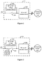
- FIG. 1 is a schematic diagram of a grid-connected single-stage photovoltaic inverter according to a first embodiment of the present disclosure.
- the grid-connected single-stage photovoltaic inverter 10 includes a DC to AC inverter circuit 200, a DC to DC voltage booster circuit 100 and a bypass element 300.
- An output of the DC to AC inverter circuit 200 is connected to an alternating current grid.
- the DC to DC voltage booster circuit 100 is connected in series between a photovoltaic array PV and the DC to AC inverter circuit 200.
- the bypass element 300 is connected in parallel with the DC to DC voltage booster circuit 100.
- a power capacity Pdc of the DC to DC voltage booster circuit 100 is less than a power capacity Pac of the DC to AC inverter circuit 200.
- a parallel circuit in which the DC to DC voltage booster circuit and the bypass element are connected in parallel is connected to a front end of the DC to AC inverter circuit of a conventional grid-connected single-stage photovoltaic inverter.
- the DC to DC voltage booster circuit operates in a situation of low radiation such as in the morning and evening, or on a cloudy or rainy day, to improve a direct current bus voltage of the grid-connected photovoltaic inverter.
- the grid-connected photovoltaic inverter meets a grid connection condition, and can perform grid-connected power generation, which increases power generation amount.
- the rated power capacity Pdc of the DC to DC voltage booster circuit is less than the rated power capacity Pac of the DC to AC inverter circuit, investment cost is greatly reduced. Benefits for investment cost recovery are significant, especially in a case of a larger power station which needs multiple grid-connected photovoltaic inverters.
- configuration of the rated power capacities of the DC to DC voltage booster circuit and the DC to AC inverter circuit may be: Pdc ⁇ 0.5Pac, which is specifically determined based on factors such as radiation of an installation location and historical weather situations.
- a DC to AC inverter circuit having a rated power capacity of 100KW is taken as an example.
- a conventional though is to provide a DC to DC voltage booster circuit having a matched power.
- a range for configuring a rated power capacity of the DC to DC voltage booster circuit is from 0 to 50KW, and the power may be 10KW. Compared with the solution of providing a DC to DC voltage booster circuit having a matched power, investment cost is greatly reduced while power generation amount is increased.
- FIG. 2 shows a grid-connected single-stage photovoltaic inverter according to a second embodiment of the present disclosure.
- the grid-connected single-stage photovoltaic inverter 20 further includes a control circuit 400 configured to control the bypass element 300 to be turned on or turned off.
- the control circuit 400 controls the bypass element 300 to be turned off and controls the DC to DC voltage booster circuit 100 to operate.
- the control circuit 400 controls the bypass element 300 to be turned on and controls the DC to DC voltage booster circuit 100 not to operate.
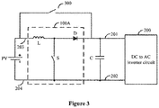
- FIG. 3 is schematic diagram of a DC to DC voltage booster circuit according to an embodiment of the present disclosure.
- a direct current bus capacitor C is connected between the DC to DC voltage booster circuit 100A and the DC to AC inverter circuit 200.
- the DC to DC voltage booster circuit 100A includes an inductor L, a diode D and a first switch S.
- a first terminal of the inductor L is connected to a first terminal of the bypass element 300 to serve as a positive input electrode 203 of the DC to DC voltage booster circuit 100A.
- the positive input electrode 203 of the DC to DC voltage booster circuit 100A is connected to a positive electrode of the photovoltaic array PV.
- a second terminal of the inductor L is connected to an anode of the diode D.
- a cathode of the diode D is connected to a second terminal of the bypass element 300 to serve as a positive output electrode of the DC to DC voltage booster circuit 100A.
- the positive output electrode of the DC to DC voltage booster circuit 100A is connected to a positive electrode 201 of a direct current bus of the DC to AC inverter circuit 200.
- a first terminal of the first switch S is connected to a common connection point of the inductor L and the diode D.
- a second terminal of the first switch S is connected to a negative electrode of the DC to DC voltage booster circuit 100A.
- the negative electrode of the DC to DC voltage booster circuit 100A is connected to a negative electrode of the photovoltaic array PV and a negative electrode 202 of the direct current bus of the DC to AC inverter circuit 200.
- the DC to DC voltage booster circuit may be of any circuit structure which can achieve a voltage boosting function, such as a non-isolated forward circuit, a non-isolated flyback circuit or a non-isolated push-pull circuit, and is not limited by the present disclosure.
- the bypass element 300 may be any electrical element which can achieve a function of turning on and turning off a circuit, such as an electric switch, a high-voltage direct-current relay, a high-voltage MOSFET or a high-voltage IGBT, or may be a circuit which can achieve the same function.
- the DC to AC inverter circuit may employ any circuit topology which can convert a direct current into an alternating current, such as a two-level topology, or may employ a multilevel topology such as three-level topology or five-level topology, and is not limited by the present disclosure.
- the DC to AC inverter circuit may be a single-phase inverter circuit, or may be a three-phase inverter circuit, which is not limited by the present disclosure.
- a DC to DC voltage booster circuit applied to the grid-connected single-stage photovoltaic inverter described above is further provided according to an embodiment of the present disclosure. Reference is made to the above descriptions for details.
- a control method for the grid-connected single-stage photovoltaic inverter described above is further provided according to an embodiment of the present disclosure.
- the method includes steps S11 to S 15.
- step S11 a voltage Upv_mppt at a maximum power point of the photovoltaic array is obtained.
- step S12 an output power Ppv of the photovoltaic array is obtained.
- step S 13 the voltage Upv_mppt at the maximum power point of the photovoltaic array is compared with a voltage peak of the alternating current grid.
- step S14 the output power Ppv of the photovoltaic array is compared with the rated power capacity Pdc of the DC to DC voltage booster circuit.
- step S15 the bypass element 300 is controlled to be turned on or turned off and the DC to DC voltage booster circuit is controlled to operate or not to operate based on a comparison result.
- controlling the bypass element 300 to be turned on or turned off and controlling the DC to DC voltage booster circuit to operate or not to operate based on a comparison result in step S15 includes: controlling the bypass element 300 to be turned off and controlling the DC to DC voltage booster circuit to operate, in a case that the voltage Upv_mppt at the maximum power point of the photovoltaic array is less than the voltage peak of the alternating current grid or in a case that the output power Ppv of the photovoltaic array is less than the rated power capacity Pdc of the DC to DC voltage booster circuit; or controlling the bypass element 300 to be turned on and controlling the DC to DC voltage booster circuit not to operate, in a case that the voltage Upv_mppt at the maximum power point of the photovoltaic array is not less than the voltage peak of the alternating current grid or in a case that the output power Ppv of the photovoltaic array is not less than the rated power capacity Pdc of the DC to DC voltage booster circuit.
- a photovoltaic power generation system is further provided according to an embodiment of the present disclosure, which includes the grid-connected single-stage photovoltaic inverter according to the above embodiments and a photovoltaic array.
- a rated power capacity of an inverter circuit is at least 100KW; in a case that a conventional grid-connected two-stage photovoltaic inverter (simply referred to as symmetric DC-DC+INV) of a voltage booster circuit (DC-DC) and an inverter circuit (INV) having matched powers is provided for the photovoltaic power generation system, rated power capacities of the booster circuit and the inverter circuit need to be matched and to be at least 100KW; in a case that the grid-connected single-stage photovoltaic inverter (simply referred to as asymmetric DC-DC+INV) according to the embodiments of the present disclosure is provided for the photovoltaic power generation system, a rated power capacity of an inverter circuit is
- an output power of the photovoltaic array is up to 8KW in a situation of low radiation such as in the morning and evening, or on a cloudy or rainy day. Since the single INV system does not include a DC-DC, the single INV system does not meet a grid connection condition, and can not perform grid-connected power generation. Both the symmetric DC-DC+INV and the asymmetric DC-DC+INV can generate power normally. It is assumed that there are 365 days in one year and a radiation condition for the photovoltaic power generation system is the same for every day, on average, a total time period in which the output power of the photovoltaic array for every day can not be ignored and can not meet the grid connection condition of the single INV.
- the single INV system is cheapest, and the symmetric DC-DC+INV is most expensive. Extra annual power generation revenue of the single INV is 0, and extra annual power generation revenue of the symmetric DC-DC+INV is equal to that of the asymmetric DC-DC+INV. It can be seen that, the photovoltaic power generation system provided with the asymmetric DC-DC+INV is most cost effective and has the fastest speed of investment cost recovery.
- a parallel circuit in which the DC to DC voltage booster circuit and the bypass element are connected in parallel is connected in series between the photovoltaic array and the DC to AC inverter circuit, and the rated power capacity Pdc of the DC to DC voltage booster circuit is less than the rated power capacity Pac of the DC to AC inverter circuit.
- the DC to DC voltage booster circuit is controlled not to operate in a time period in which radiation is high, such as the daytime, so that the operating efficiency of the grid-connected single-stage photovoltaic inverter is high.
- the DC to DC voltage booster circuit is controlled to operate in a situation of low radiation such as in the morning and evening, or on a cloudy or rainy day, to improve a direct current bus voltage of the grid-connected photovoltaic inverter.
- the grid-connected photovoltaic inverter meets a grid connection condition, and can perform grid-connected power generation, which increases power generation amount.
- the rated power capacity Pdc of the DC to DC voltage booster circuit is less than the rated power capacity Pac of the DC to AC inverter circuit, investment cost is greatly reduced, and cost recovery is speeded up.
Landscapes
- Engineering & Computer Science (AREA)
- Power Engineering (AREA)
- Inverter Devices (AREA)
- Direct Current Feeding And Distribution (AREA)
- Charge And Discharge Circuits For Batteries Or The Like (AREA)
- Supply And Distribution Of Alternating Current (AREA)
Abstract
Description
- The present application claims the priority to Chinese Patent Application No.
201410335465.2 - The present disclosure relates to a grid-connected single-stage photovoltaic inverter, and in particular to a grid-connected single-stage photovoltaic inverter including a DC to AC inverter circuit, and a control method and an application thereof.
- In order to perform normal grid-connected power generation, a grid-connected photovoltaic inverter is required to meet a predetermined grid connection condition. For example, a direct current bus voltage of the grid-connected photovoltaic inverter is required not to be less than a peak of a grid voltage. To improve operating efficiency of the grid-connected photovoltaic inverter, inverter manufacturers usually arrange many solar panels to improve an open-circuit voltage of a photovoltaic array, or arrange a DC to DC voltage booster circuit which matches a DC to AC inverter circuit in terms of a power capacity at a front end of the DC to AC inverter circuit, to meet the grid connection condition.
- For a situation that the DC to DC voltage booster circuit which matches the DC to AC inverter circuit in terms of the power capacity is arranged at the front end of the DC to AC inverter circuit, a general design thought is to achieve, by the DC to DC voltage booster circuit at the front end, a voltage boosting function for a voltage outputted by the photovoltaic array. In this case, the photovoltaic array does not need to be provided with many solar panels. In practice, the design though has the following shortcomings: a high cost due to the power capacity of the DC to DC voltage booster circuit matching the power capacity of the DC to AC inverter circuit, and low overall efficiency of the inverter due to the fact that a great switching loss is caused since the DC to DC voltage booster circuit needs to operate together with the DC to AC inverter circuit for a long time. As an improvement, a contactor is connected in parallel with the DC to DC voltage booster circuit. In some special situations, for example, adequate sunlight being available and the grid connection condition being met, the contactor is turned on, and the DC to DC voltage booster circuit may stop operating for a short time. The improvement can not solve the problem of a high cost, while the switching loss is reduced and the conversion efficiency is improved.
- For a situation in the conventional technology that a grid-connected single-stage photovoltaic inverter including a DC to AC inverter circuit is used, inverter manufacturers usually arrange many photovoltaic panels to improve an open-circuit voltage of a photovoltaic array. The grid-connected single-stage photovoltaic inverter has advantages such as a simple circuit, an output power up to several megawatts and a low unit cost of power generation, and is widely applied to larger photovoltaic power stations. Although an appropriate number of photovoltaic panels are provided, the grid connection condition still can not be met in a situation of low radiation such as in the morning and evening, or on a cloudy or rainy day. Hence, the grid-connected photovoltaic inverter can not perform grid-connected power generation, which results in a loss in power generation amount.
- In view of the above, the present disclosure is to provide a grid-connected single-stage photovoltaic inverter which can increase power generation amount as compared with a conventional grid-connected single-stage photovoltaic inverter.
- A grid-connected single-stage photovoltaic inverter is provided according to the present disclosure, which includes a DC to AC inverter circuit, a DC to DC voltage booster circuit and a bypass element. An output of the DC to AC inverter circuit is connected to an alternating current grid. The DC to DC voltage booster circuit is connected in series between a photovoltaic array and the DC to AC inverter circuit. The bypass element is connected in parallel with the DC to DC voltage booster circuit. A rated power capacity Pdc of the DC to DC voltage booster circuit is less than a rated power capacity Pac of the DC to AC inverter circuit.
- Further, the rated power capacity Pdc of the DC to DC voltage booster circuit being less than the rated power capacity Pac of the DC to AC inverter circuit includes: Pdc≤0.5Pac.
- Further, the grid-connected single-stage photovoltaic inverter further includes a control circuit configured to control the bypass element to be turned on or turned off. The control circuit controls the bypass element to be turned off and controls the DC to DC voltage booster circuit to operate, in a case that a voltage Upv_mppt at a maximum power point of the photovoltaic array is less than a voltage peak of the alternating current grid or in a case that an output power Ppv of the photovoltaic array is less than the rated power capacity Pdc of the DC to DC voltage booster circuit. Or, the control circuit controls the bypass element to be turned on and controls the DC to DC voltage booster circuit not to operate, in a case that a voltage Upv_mppt at a maximum power point of the photovoltaic array is not less than a voltage peak of the alternating current grid or in a case that an output power Ppv of the photovoltaic array is not less than the rated power capacity Pdc of the DC to DC voltage booster circuit.
- Further, the bypass element includes an electric switch, a high-voltage direct-current relay, a high-voltage MOSFET or a high-voltage IGBT.
- Further, the DC to AC inverter circuit employs a two-level topology or a multilevel topology.
- Further, the DC to AC inverter circuit includes a three-phase inverter circuit or a single-phase inverter circuit.
- A DC to DC voltage booster circuit applied to the grid-connected single-stage photovoltaic inverter described above is further provided according to the present disclosure.
- A photovoltaic power generation system is further provided according to the present disclosure, which includes the grid-connected single-stage photovoltaic inverter described above and a photovoltaic array.
- A control method for the grid-connected single-stage photovoltaic inverter described above is further provided according to the present disclosure, and the control method includes: obtaining a voltage Upv_mppt at a maximum power point of the photovoltaic array; obtaining an output power Ppv of the photovoltaic array; comparing the voltage Upv_mppt at the maximum power point of the photovoltaic array with a voltage peak of the alternating current grid; comparing the output power Ppv of the photovoltaic array with the rated power capacity Pdc of the DC to DC voltage booster circuit; and controlling the bypass element to be turned on or turned off and controlling the DC to DC voltage booster circuit to operate or not to operate based on a comparison result.
- Further, the controlling the bypass element to be turned on or turned off and controlling the DC to DC voltage booster circuit to operate or not to operate based on a comparison result includes: controlling the bypass element to be turned off and controlling the DC to DC voltage booster circuit to operate, in a case that the voltage Upv_mppt at the maximum power point of the photovoltaic array is less than the voltage peak of the alternating current grid or in a case that the output power Ppv of the photovoltaic array is less than the rated power capacity Pdc of the DC to DC voltage booster circuit; and controlling the bypass element to be turned on and controlling the DC to DC voltage booster circuit not to operate, in a case that the voltage Upv_mppt at the maximum power point of the photovoltaic array is not less than the voltage peak of the alternating current grid or in a case that the output power Ppv of the photovoltaic array is not less than the rated power capacity Pdc of the DC to DC voltage booster circuit.
- Compared with the conventional technology, the present disclosure has the following advantages.
- Compared with a conventional grid-connected single-stage photovoltaic inverter, in the grid-connected single-stage photovoltaic inverter according to the present disclosure, a parallel circuit in which the DC to DC voltage booster circuit and the bypass element are connected in parallel is connected in series between the photovoltaic array and the DC to AC inverter circuit, and the rated power capacity Pdc of the DC to DC voltage booster circuit is less than the rated power capacity Pac of the DC to AC inverter circuit. The DC to DC voltage booster circuit is controlled not to operate in a long time period in which radiation is high, such as the daytime, thereby improving efficiency. The DC to DC voltage booster circuit is controlled to operate in a situation of low radiation such as in the morning and evening, or on a cloudy or rainy day, to improve a direct current bus voltage of the grid-connected photovoltaic inverter. As a result, the grid-connected photovoltaic inverter meets a grid connection condition, and can perform grid-connected power generation, which increases power generation amount. In addition, since the rated power capacity Pdc of the DC to DC voltage booster circuit is less than the rated power capacity Pac of the DC to AC inverter circuit, investment cost is greatly reduced.
- In order to illustrate technical solutions in embodiments of the present disclosure or in the conventional technology more clearly, drawings used in the description of the embodiments or the conventional technology are introduced briefly hereinafter. Apparently, the drawings described hereinafter merely illustrate some embodiments of the present disclosure, and other drawings may be obtained by those skilled in the art based on these drawings without any creative efforts.
-
Figure 1 is a schematic diagram of a grid-connected single-stage photovoltaic inverter according to a first embodiment of the present disclosure; -
Figure 2 is a schematic diagram of a grid-connected single-stage photovoltaic inverter according to a second embodiment of the present disclosure; and -
Figure 3 is a schematic diagram of a DC to DC voltage booster circuit according to an embodiment of the present disclosure. - In order to make the above object, features, and advantages of the present disclosure clearer, embodiments of the present disclosure are described in detail hereinafter in conjunction with the drawings.
- A grid-connected single-stage photovoltaic inverter, which can increase power generation amount as compared with a conventional grid-connected single-stage photovoltaic inverter, is provided according to the present disclosure.
- Reference is made to
Figure 1 , which is a schematic diagram of a grid-connected single-stage photovoltaic inverter according to a first embodiment of the present disclosure. The grid-connected single-stagephotovoltaic inverter 10 includes a DC toAC inverter circuit 200, a DC to DCvoltage booster circuit 100 and abypass element 300. An output of the DC toAC inverter circuit 200 is connected to an alternating current grid. The DC to DCvoltage booster circuit 100 is connected in series between a photovoltaic array PV and the DC toAC inverter circuit 200. Thebypass element 300 is connected in parallel with the DC to DCvoltage booster circuit 100. A power capacity Pdc of the DC to DCvoltage booster circuit 100 is less than a power capacity Pac of the DC toAC inverter circuit 200. - In the grid-connected single-stage photovoltaic inverter according to the embodiment of the present disclosure, a parallel circuit in which the DC to DC voltage booster circuit and the bypass element are connected in parallel is connected to a front end of the DC to AC inverter circuit of a conventional grid-connected single-stage photovoltaic inverter. As a result, an operating range of direct current input voltage is expanded for the grid-connected photovoltaic inverter. The DC to DC voltage booster circuit operates in a situation of low radiation such as in the morning and evening, or on a cloudy or rainy day, to improve a direct current bus voltage of the grid-connected photovoltaic inverter. In this case, the grid-connected photovoltaic inverter meets a grid connection condition, and can perform grid-connected power generation, which increases power generation amount. In addition, since the rated power capacity Pdc of the DC to DC voltage booster circuit is less than the rated power capacity Pac of the DC to AC inverter circuit, investment cost is greatly reduced. Benefits for investment cost recovery are significant, especially in a case of a larger power station which needs multiple grid-connected photovoltaic inverters.
- Optionally, configuration of the rated power capacities of the DC to DC voltage booster circuit and the DC to AC inverter circuit may be: Pdc≤0.5Pac, which is specifically determined based on factors such as radiation of an installation location and historical weather situations. A DC to AC inverter circuit having a rated power capacity of 100KW is taken as an example. For solving a technical problem that grid-connected power generation can not be performed in a situation of low radiation such as in the morning and evening, or on a cloudy or rainy day, a conventional though is to provide a DC to DC voltage booster circuit having a matched power. In the present disclosure, a range for configuring a rated power capacity of the DC to DC voltage booster circuit is from 0 to 50KW, and the power may be 10KW. Compared with the solution of providing a DC to DC voltage booster circuit having a matched power, investment cost is greatly reduced while power generation amount is increased.
- Reference is made to
Figure 2 , which shows a grid-connected single-stage photovoltaic inverter according to a second embodiment of the present disclosure. Compared with the first embodiment, the grid-connected single-stagephotovoltaic inverter 20 further includes acontrol circuit 400 configured to control thebypass element 300 to be turned on or turned off. - In a case that a voltage Upv_mppt at a maximum power point of the photovoltaic array PV is less than a voltage peak of the alternating current grid or in a case that an output power Ppv of the photovoltaic array PV is less than the rated power capacity Pdc of the DC to DC
voltage booster circuit 100, thecontrol circuit 400 controls thebypass element 300 to be turned off and controls the DC to DCvoltage booster circuit 100 to operate. In a case that a voltage Upv_mppt at a maximum power point of the photovoltaic array PV is not less than a voltage peak of the alternating current grid or in a case that an output power Ppv of the photovoltaic array is not less than the rated power capacity Pdc of the DC to DC voltage booster circuit, thecontrol circuit 400 controls thebypass element 300 to be turned on and controls the DC to DCvoltage booster circuit 100 not to operate. - Reference is made to
Figure 3 , which is schematic diagram of a DC to DC voltage booster circuit according to an embodiment of the present disclosure. A direct current bus capacitor C is connected between the DC to DCvoltage booster circuit 100A and the DC toAC inverter circuit 200. The DC to DCvoltage booster circuit 100A includes an inductor L, a diode D and a first switch S. A first terminal of the inductor L is connected to a first terminal of thebypass element 300 to serve as apositive input electrode 203 of the DC to DCvoltage booster circuit 100A. Thepositive input electrode 203 of the DC to DCvoltage booster circuit 100A is connected to a positive electrode of the photovoltaic array PV. A second terminal of the inductor L is connected to an anode of the diode D. A cathode of the diode D is connected to a second terminal of thebypass element 300 to serve as a positive output electrode of the DC to DCvoltage booster circuit 100A. The positive output electrode of the DC to DCvoltage booster circuit 100A is connected to apositive electrode 201 of a direct current bus of the DC toAC inverter circuit 200. A first terminal of the first switch S is connected to a common connection point of the inductor L and the diode D. A second terminal of the first switch S is connected to a negative electrode of the DC to DCvoltage booster circuit 100A. The negative electrode of the DC to DCvoltage booster circuit 100A is connected to a negative electrode of the photovoltaic array PV and anegative electrode 202 of the direct current bus of the DC toAC inverter circuit 200. - As an alternative, the DC to DC voltage booster circuit may be of any circuit structure which can achieve a voltage boosting function, such as a non-isolated forward circuit, a non-isolated flyback circuit or a non-isolated push-pull circuit, and is not limited by the present disclosure.
- In all embodiments of the present disclosure, the
bypass element 300 may be any electrical element which can achieve a function of turning on and turning off a circuit, such as an electric switch, a high-voltage direct-current relay, a high-voltage MOSFET or a high-voltage IGBT, or may be a circuit which can achieve the same function. - The DC to AC inverter circuit according to any one of the embodiments of the present disclosure may employ any circuit topology which can convert a direct current into an alternating current, such as a two-level topology, or may employ a multilevel topology such as three-level topology or five-level topology, and is not limited by the present disclosure.
- Further, the DC to AC inverter circuit according to any of one of the embodiments of the present disclosure may be a single-phase inverter circuit, or may be a three-phase inverter circuit, which is not limited by the present disclosure.
- A DC to DC voltage booster circuit applied to the grid-connected single-stage photovoltaic inverter described above is further provided according to an embodiment of the present disclosure. Reference is made to the above descriptions for details.
- A control method for the grid-connected single-stage photovoltaic inverter described above is further provided according to an embodiment of the present disclosure. The method includes steps S11 to S 15.
- In step S11, a voltage Upv_mppt at a maximum power point of the photovoltaic array is obtained.
- In step S12, an output power Ppv of the photovoltaic array is obtained.
- In step S 13, the voltage Upv_mppt at the maximum power point of the photovoltaic array is compared with a voltage peak of the alternating current grid.
- In step S14, the output power Ppv of the photovoltaic array is compared with the rated power capacity Pdc of the DC to DC voltage booster circuit.
- In step S15, the
bypass element 300 is controlled to be turned on or turned off and the DC to DC voltage booster circuit is controlled to operate or not to operate based on a comparison result. - Further, the controlling the
bypass element 300 to be turned on or turned off and controlling the DC to DC voltage booster circuit to operate or not to operate based on a comparison result in step S15 includes: controlling thebypass element 300 to be turned off and controlling the DC to DC voltage booster circuit to operate, in a case that the voltage Upv_mppt at the maximum power point of the photovoltaic array is less than the voltage peak of the alternating current grid or in a case that the output power Ppv of the photovoltaic array is less than the rated power capacity Pdc of the DC to DC voltage booster circuit; or controlling thebypass element 300 to be turned on and controlling the DC to DC voltage booster circuit not to operate, in a case that the voltage Upv_mppt at the maximum power point of the photovoltaic array is not less than the voltage peak of the alternating current grid or in a case that the output power Ppv of the photovoltaic array is not less than the rated power capacity Pdc of the DC to DC voltage booster circuit. - A photovoltaic power generation system is further provided according to an embodiment of the present disclosure, which includes the grid-connected single-stage photovoltaic inverter according to the above embodiments and a photovoltaic array.
- Benefits of the present disclosure are described with an example of a photovoltaic power generation system of 100KW.
- For the photovoltaic power generation system of 100KW provided with the same photovoltaic array: in a case that a conventional grid-connected single-stage photovoltaic inverter (simply referred to as single INV) is provided for the photovoltaic power generation system, a rated power capacity of an inverter circuit is at least 100KW; in a case that a conventional grid-connected two-stage photovoltaic inverter (simply referred to as symmetric DC-DC+INV) of a voltage booster circuit (DC-DC) and an inverter circuit (INV) having matched powers is provided for the photovoltaic power generation system, rated power capacities of the booster circuit and the inverter circuit need to be matched and to be at least 100KW; in a case that the grid-connected single-stage photovoltaic inverter (simply referred to as asymmetric DC-DC+INV) according to the embodiments of the present disclosure is provided for the photovoltaic power generation system, a rated power capacity of an inverter circuit is at least 100KW, and a rated power capacity of the voltage booster circuit is assumed to be 8KW. Cost of the voltage booster circuit is 0.1 Yuan/watt, and cost of the inverter circuit is 0.2 Yuan/watt.
- It is assumed that an output power of the photovoltaic array is up to 8KW in a situation of low radiation such as in the morning and evening, or on a cloudy or rainy day. Since the single INV system does not include a DC-DC, the single INV system does not meet a grid connection condition, and can not perform grid-connected power generation. Both the symmetric DC-DC+INV and the asymmetric DC-DC+INV can generate power normally. It is assumed that there are 365 days in one year and a radiation condition for the photovoltaic power generation system is the same for every day, on average, a total time period in which the output power of the photovoltaic array for every day can not be ignored and can not meet the grid connection condition of the single INV. Through calculation based on a current subsidy of 1.5 Yuan/watt, design parameters and power generation amount of the single INV, the symmetric DC-DC+INV and the asymmetric DC-DC+INV are listed as follows.
single INV symmetric DC-DC+INV asymmetric DC-DC+INV power of DC-DC 0 100KW 8KW power of INV 100KW 100KW 100KW cost of DC-DC 0 10000 Yuan 800 Yuan cost of INV 20000 Yuan 20000 Yuan 20000 Yuan total cost of inverter 20000 Yuan 30000 Yuan 20800 Yuan extra daily power generation amount 0 8KWh 8KWh extra annual power generation revenue 0 4380 Yuan 4380 Yuan - For the three systems, the single INV system is cheapest, and the symmetric DC-DC+INV is most expensive. Extra annual power generation revenue of the single INV is 0, and extra annual power generation revenue of the symmetric DC-DC+INV is equal to that of the asymmetric DC-DC+INV. It can be seen that, the photovoltaic power generation system provided with the asymmetric DC-DC+INV is most cost effective and has the fastest speed of investment cost recovery.
- Compared with a conventional grid-connected single-stage photovoltaic inverter, in the grid-connected single-stage photovoltaic inverter according to the present disclosure, a parallel circuit in which the DC to DC voltage booster circuit and the bypass element are connected in parallel is connected in series between the photovoltaic array and the DC to AC inverter circuit, and the rated power capacity Pdc of the DC to DC voltage booster circuit is less than the rated power capacity Pac of the DC to AC inverter circuit. The DC to DC voltage booster circuit is controlled not to operate in a time period in which radiation is high, such as the daytime, so that the operating efficiency of the grid-connected single-stage photovoltaic inverter is high. The DC to DC voltage booster circuit is controlled to operate in a situation of low radiation such as in the morning and evening, or on a cloudy or rainy day, to improve a direct current bus voltage of the grid-connected photovoltaic inverter. As a result, the grid-connected photovoltaic inverter meets a grid connection condition, and can perform grid-connected power generation, which increases power generation amount. In addition, since the rated power capacity Pdc of the DC to DC voltage booster circuit is less than the rated power capacity Pac of the DC to AC inverter circuit, investment cost is greatly reduced, and cost recovery is speeded up.
- The above descriptions are only preferred embodiments of the present disclosure and should not be interpreted as limiting of the present disclosure in any form. Although the present disclosure is disclosed by the above preferred embodiments, the preferred embodiments are not to limit the present disclosure. Various changes and modifications to the technical solutions of the present disclosure can be made by those skilled in the art based on the above method and technical contents within the scope of the technical solutions of the present disclosure. Alternatively, the technical solutions of the present disclosure can be modified into equivalent embodiments. Therefore, any simple changes, equivalents and modifications which do not depart from the technical solutions of the present disclosure and are made based on the essence of the present disclosure also fall within the protection scope of the technical solutions of the present disclosure.
Claims (10)
- A grid-connected single-stage photovoltaic inverter, comprising:a DC to AC inverter circuit, wherein an output of the DC to AC inverter circuit is connected to an alternating current grid;a DC to DC voltage booster circuit connected in series between a photovoltaic array and the DC to AC inverter circuit; anda bypass element connected in parallel with the DC to DC voltage booster circuit, whereina rated power capacity Pdc of the DC to DC voltage booster circuit is less than a rated power capacity Pac of the DC to AC inverter circuit.
- The grid-connected single-stage photovoltaic inverter according to claim 1, wherein the rated power capacity Pdc of the DC to DC voltage booster circuit being less than the rated power capacity Pac of the DC to AC inverter circuit comprises: Pdc≤0.5Pac.
- The grid-connected single-stage photovoltaic inverter according to claim 1, further comprising: a control circuit configured to control the bypass element to be turned on or turned off; wherein
the control circuit controls the bypass element to be turned off and controls the DC to DC voltage booster circuit to operate, in a case that a voltage Upv_mppt at a maximum power point of the photovoltaic array is less than a voltage peak of the alternating current grid or in a case that an output power Ppv of the photovoltaic array is less than the rated power capacity Pdc of the DC to DC voltage booster circuit; or
the control circuit controls the bypass element to be turned on and controls the DC to DC voltage booster circuit not to operate, in a case that a voltage Upv_mppt at a maximum power point of the photovoltaic array is not less than a voltage peak of the alternating current grid or in a case that an output power Ppv of the photovoltaic array is not less than the rated power capacity Pdc of the DC to DC voltage booster circuit. - The grid-connected single-stage photovoltaic inverter according to any one of claims 1 to 3, wherein the bypass element comprises an electric switch, a high-voltage direct-current relay, a high-voltage MOSFET or a high-voltage IGBT.
- The grid-connected single-stage photovoltaic inverter according to any one of claims 1 to 3, wherein the DC to AC inverter circuit employs a two-level topology or a multilevel topology.
- The grid-connected single-stage photovoltaic inverter according to any one of claims 1 to 3, wherein the DC to AC inverter circuit comprises a three-phase inverter circuit or a single-phase inverter circuit.
- A DC to DC voltage booster circuit applied to the grid-connected single-stage photovoltaic inverter according to any one of claims 1 to 3.
- A photovoltaic power generation system, comprising the grid-connected single-stage photovoltaic inverter according to any one of claims 1 to 3 and a photovoltaic array.
- A control method for the grid-connected single-stage photovoltaic inverter according to claim 1 or claim 2, comprising:obtaining a voltage Upv_mppt at a maximum power point of the photovoltaic array;obtaining an output power Ppv of the photovoltaic array;comparing the voltage Upv_mppt at the maximum power point of the photovoltaic array with a voltage peak of the alternating current grid;comparing the output power Ppv of the photovoltaic array with the rated power capacity Pdc of the DC to DC voltage booster circuit; andcontrolling the bypass element to be turned on or turned off and controlling the DC to DC voltage booster circuit to operate or not to operate based on a comparison result.
- The control method for the grid-connected single-stage photovoltaic inverter according to claim 9, wherein the controlling the bypass element to be turned on or turned off and controlling the DC to DC voltage booster circuit to operate or not to operate based on a comparison result comprises:controlling the bypass element to be turned off and controlling the DC to DC voltage booster circuit to operate, in a case that the voltage Upv_mppt at the maximum power point of the photovoltaic array is less than the voltage peak of the alternating current grid or in a case that the output power Ppv of the photovoltaic array is less than the rated power capacity Pdc of the DC to DC voltage booster circuit; orcontrolling the bypass element to be turned on and controlling the DC to DC voltage booster circuit not to operate, in a case that the voltage Upv_mppt at the maximum power point of the photovoltaic array is not less than the voltage peak of the alternating current grid or in a case that the output power Ppv of the photovoltaic array is not less than the rated power capacity Pdc of the DC to DC voltage booster circuit.
Applications Claiming Priority (2)
| Application Number | Priority Date | Filing Date | Title |
|---|---|---|---|
| CN201410335465.2A CN104158208A (en) | 2014-07-15 | 2014-07-15 | Single-stage photovoltaic grid-connected inverter, as well as control method and application thereof |
| PCT/CN2015/083628 WO2016008382A1 (en) | 2014-07-15 | 2015-07-09 | Single-stage photovoltaic grid-connected inverter and control method and application thereof |
Publications (3)
| Publication Number | Publication Date |
|---|---|
| EP3171478A1 true EP3171478A1 (en) | 2017-05-24 |
| EP3171478A4 EP3171478A4 (en) | 2018-03-28 |
| EP3171478B1 EP3171478B1 (en) | 2022-10-05 |
Family
ID=51883651
Family Applications (1)
| Application Number | Title | Priority Date | Filing Date |
|---|---|---|---|
| EP15821660.6A Active EP3171478B1 (en) | 2014-07-15 | 2015-07-09 | Photovoltaic grid-connected inverter and control method thereof |
Country Status (6)
| Country | Link |
|---|---|
| US (1) | US20170133857A1 (en) |
| EP (1) | EP3171478B1 (en) |
| JP (1) | JP6424365B2 (en) |
| CN (1) | CN104158208A (en) |
| ES (1) | ES2928308T3 (en) |
| WO (1) | WO2016008382A1 (en) |
Cited By (3)
| Publication number | Priority date | Publication date | Assignee | Title |
|---|---|---|---|---|
| CN113205664A (en) * | 2021-05-08 | 2021-08-03 | 杭州华电半山发电有限公司 | Detection and alarm method based on 9FA gas-steam combined cycle unit |
| EP3893380A4 (en) * | 2018-12-29 | 2021-11-24 | Huawei Technologies Co., Ltd. | INVERTER |
| CN114094631A (en) * | 2021-12-03 | 2022-02-25 | 国网新疆电力有限公司电力科学研究院 | MPPT control method suitable for concentrated photovoltaic DC-DC converter |
Families Citing this family (87)
| Publication number | Priority date | Publication date | Assignee | Title |
|---|---|---|---|---|
| CN104158208A (en) * | 2014-07-15 | 2014-11-19 | 阳光电源股份有限公司 | Single-stage photovoltaic grid-connected inverter, as well as control method and application thereof |
| CN104638971B (en) * | 2015-02-13 | 2018-04-03 | 河海大学 | A kind of photovoltaic combining inverter and its control method |
| CN105337520A (en) * | 2015-12-11 | 2016-02-17 | 珠海格力电器股份有限公司 | Photovoltaic grid-connected converter, photovoltaic power supply system and electric appliance |
| CN107546836B (en) | 2016-06-23 | 2019-11-26 | 维谛技术有限公司 | A kind of ups power |
| CN106787891B (en) * | 2017-03-06 | 2023-07-07 | 云南电网有限责任公司电力科学研究院 | Five-level inverter |
| CN107565600B (en) * | 2017-09-15 | 2020-04-03 | 华为数字技术(苏州)有限公司 | Photovoltaic power optimizer and its control method, device, and photovoltaic power generation system |
| CN107800184B (en) * | 2017-11-10 | 2020-11-17 | 湖南省保利光电科技有限责任公司 | quasi-MPPT charging device for small 12V photovoltaic application system |
| CN107959433B (en) * | 2017-12-21 | 2020-08-28 | 阳光电源股份有限公司 | Inverter and inversion system for inhibiting leakage current |
| US10381834B1 (en) * | 2018-03-08 | 2019-08-13 | Omron Corporation | Power conditioner and power system |
| AU2019257598B2 (en) | 2018-04-24 | 2025-01-02 | Becton, Dickinson And Company | Multi-laser systems having modified beam profiles and methods of use thereof |
| CN112154317B (en) | 2018-04-26 | 2024-11-08 | 贝克顿·迪金森公司 | Particle Analyzer Characterization and Sorting |
| EP3785016A4 (en) | 2018-04-26 | 2022-02-09 | Becton, Dickinson and Company | BIEXPONENTIAL TRANSFORMATION FOR PARTICLE SORTERS |
| CN112449680B (en) | 2018-06-19 | 2024-08-09 | 贝克顿·迪金森公司 | Variable multiplexing switch for detector array, system and method of using the same |
| EP3814748B1 (en) | 2018-06-28 | 2026-03-25 | Becton, Dickinson and Company | Integrated pre-amplification light detection systems and methods of use thereof |
| EP3611832A1 (en) * | 2018-08-13 | 2020-02-19 | FRONIUS INTERNATIONAL GmbH | Photovoltaic inverter and method for operating the same |
| WO2020036730A1 (en) | 2018-08-15 | 2020-02-20 | Becton, Dickinson And Company | Flowrate and vacuum controlled fluid management system for a flow type particle analyzer |
| CN109039061B (en) | 2018-08-29 | 2020-03-24 | 阳光电源股份有限公司 | A multi-level BOOST device |
| EP3844482B1 (en) | 2018-08-30 | 2025-03-12 | Becton, Dickinson and Company | Characterization and sorting for particle analyzers |
| EP3874254B1 (en) | 2018-10-30 | 2025-04-30 | Becton, Dickinson and Company | Particle sorting module with alignment window, systems and methods of use thereof |
| US11009400B2 (en) | 2018-12-28 | 2021-05-18 | Becton, Dickinson And Company | Methods for spectrally resolving fluorophores of a sample and systems for same |
| US11085868B2 (en) | 2019-02-08 | 2021-08-10 | Becton, Dickinson And Company | Droplet sorting decision modules, systems and methods of use thereof |
| EP3867627B1 (en) | 2019-03-29 | 2023-10-25 | Becton, Dickinson and Company | Parameters for use in particle discrimination |
| WO2020231632A1 (en) | 2019-05-14 | 2020-11-19 | Becton, Dickinson And Company | Phase-calibration for imaging flow cytometry |
| US11579071B2 (en) | 2019-05-30 | 2023-02-14 | Becton, Dickinson And Company | Phase-correction of radiofrequency-multiplexed signals |
| CN112117920B (en) | 2019-06-20 | 2022-02-22 | 台达电子工业股份有限公司 | Power supply device, control method thereof and power supply system |
| WO2021007075A1 (en) | 2019-07-10 | 2021-01-14 | Becton, Dickinson And Company | Reconfigurable integrated circuits for adjusting cell sorting classification |
| CN110932310A (en) * | 2019-11-08 | 2020-03-27 | 华为技术有限公司 | A photovoltaic control device, method and system |
| US11635375B2 (en) | 2019-11-20 | 2023-04-25 | Becton, Dickinson And Company | Light detection module with adjustable sensitivity |
| CN111082686B (en) * | 2020-01-13 | 2022-04-08 | 阳光电源股份有限公司 | A multi-channel MPPT inverter and its control method |
| JP7663587B2 (en) | 2020-01-31 | 2025-04-16 | ベクトン・ディキンソン・アンド・カンパニー | Method and system for adjusting training gates to accommodate flow cytometer data - Patents.com |
| US11821830B2 (en) | 2020-02-07 | 2023-11-21 | Becton, Dickinson And Company | Clustered wavelength division light detection systems and methods of using the same |
| JP7672419B2 (en) | 2020-02-19 | 2025-05-07 | ベクトン・ディキンソン・アンド・カンパニー | Strobe laser excitation system and method of use |
| US11592386B2 (en) | 2020-02-26 | 2023-02-28 | Becton, Dickinson And Company | Light detection systems having a secondary light scatter detector and methods for using same |
| EP4111169A4 (en) | 2020-02-27 | 2023-08-09 | Becton, Dickinson and Company | METHODS FOR IDENTIFYING SATURATED DATA SIGNALS IN CELL SORTING AND RELATED SYSTEMS |
| JP2023518457A (en) | 2020-03-17 | 2023-05-01 | ベクトン・ディキンソン・アンド・カンパニー | Gain-matched amplifier for photodetection |
| WO2021211259A1 (en) | 2020-04-16 | 2021-10-21 | Becton, Dickinson And Company | Systems for light detection array multiplexing and methods for same |
| US11662297B2 (en) | 2020-04-28 | 2023-05-30 | Becton, Dickinson And Company | Method for index sorting unique phenotypes and systems for same |
| CN115917293B (en) | 2020-04-29 | 2026-02-27 | 贝克顿·迪金森公司 | Methods and systems for regulating and synchronizing detection in flow cytometry |
| CN115917315A (en) | 2020-05-05 | 2023-04-04 | 贝克顿·迪金森公司 | Method for Determining Detector Gain in a Flow Cytometer |
| WO2021225792A1 (en) | 2020-05-06 | 2021-11-11 | Becton, Dickinson And Company | Methods and systems for characterizing spillover spreading in flow cytometer data |
| CN113630088A (en) * | 2020-05-08 | 2021-11-09 | 台达电子工业股份有限公司 | Solar power generation system and detection method |
| WO2021236339A1 (en) | 2020-05-18 | 2021-11-25 | Becton, Dickinson And Company | Resolution indices for detecting heterogeneity in data and methods of use thereof |
| EP4168774A4 (en) | 2020-06-19 | 2023-12-27 | Becton, Dickinson and Company | FLOW CYTOMETER WITH ADJUSTABLE POSITION OFFSET SORT DIVERTER PLATES AND CORRESPONDING METHODS OF USE |
| EP4171819B1 (en) | 2020-06-24 | 2026-07-22 | Becton, Dickinson and Company | Flow cytometric droplet dispensing systems and methods for using the same |
| WO2021262285A1 (en) | 2020-06-26 | 2021-12-30 | Becton, Dickinson And Company | Dual excitation beams for irradiating a sample in a flow stream and methods for using same |
| WO2022066316A1 (en) | 2020-09-22 | 2022-03-31 | Becton, Dickinson And Company | Methods for continuous measurement of baseline noise in a flow cytometer and systems for same |
| CN112234649A (en) | 2020-10-15 | 2021-01-15 | 珠海格力电器股份有限公司 | Adaptive photovoltaic power supply system and control method thereof, and air conditioning unit |
| US20220120658A1 (en) | 2020-10-20 | 2022-04-21 | Becton, Dickinson And Company | Flow cytometers including tilted beam shaping optical components, and methods of using the same |
| WO2022093931A1 (en) | 2020-10-30 | 2022-05-05 | Becton, Dickinson And Company | Method and systems for characterizing and encoding a light detection system |
| WO2022103574A1 (en) | 2020-11-16 | 2022-05-19 | Becton, Dickinson And Company | Flow cyometers including light collection modules, and methods of using the same |
| US12306087B2 (en) | 2020-11-19 | 2025-05-20 | Becton, Dickinson And Company | Method for optimal scaling of cytometry data for machine learning analysis and systems for same |
| CN114080751B (en) * | 2020-11-24 | 2025-01-10 | 华为数字能源技术有限公司 | Motor controller, heat exchange system and current injection method |
| WO2022155033A1 (en) | 2021-01-13 | 2022-07-21 | Becton, Dickinson And Company | Flow cytometers including light collection enhancers, and methods of using the same |
| WO2022159190A1 (en) | 2021-01-25 | 2022-07-28 | Becton, Dickinson And Company | Method and systems for determing drop delay using scatter signals across spatially separated lasers |
| CN117098980A (en) | 2021-02-04 | 2023-11-21 | 贝克顿·迪金森公司 | Integrated optical interrogation module and how to use it |
| EP4314765A4 (en) | 2021-03-24 | 2024-10-16 | Becton, Dickinson and Company | FLOW CYTOMETER ADAPTER FOR SORTING IN A CLOSED SYSTEM AND METHOD OF USE THEREOF |
| WO2022225597A1 (en) | 2021-04-23 | 2022-10-27 | Becton, Dickinson And Company | Fluid management system for an analyzer and/or sorter type flow type particle analyzer |
| WO2022240552A1 (en) | 2021-05-14 | 2022-11-17 | Becton, Dickinson And Company | Systems for detecting light by spectral discrimination and methods for using same |
| EP4381277A4 (en) | 2021-08-04 | 2024-12-04 | Becton, Dickinson and Company | LIGHT DETECTION SYSTEMS HAVING A FIRST AND A SECOND LIGHT RECEIVER, AND METHODS OF USING THE SAME |
| US12467845B2 (en) | 2021-08-10 | 2025-11-11 | Becton, Dickinson And Company | Clamps for operably coupling an optical component to a mounting block, and methods and systems for using the same |
| US12135274B2 (en) | 2021-08-10 | 2024-11-05 | Becton, Dickinson And Company | Outlet fittings for reducing bubbles at the interface with a flow cell, and flow cytometers and methods using the same |
| CN113725903B (en) * | 2021-08-30 | 2022-08-16 | 南京邮电大学 | Distributed photovoltaic module working mode switching method based on 5G communication |
| WO2023048903A1 (en) | 2021-09-21 | 2023-03-30 | Becton, Dickinson And Company | Baseline restoration circuit |
| CA3230701A1 (en) | 2021-11-17 | 2023-05-25 | Keegan Owsley | Methods for dynamic real-time adjustment of a data acquisition parameter in a flow cytometer |
| EP4437324A4 (en) | 2021-11-24 | 2025-03-05 | Becton, Dickinson and Company | INTEGRATED FLOW CYTOMETRY DATA QUALITY CONTROL |
| KR102716720B1 (en) * | 2022-07-20 | 2024-10-15 | 한국에너지기술연구원 | Autonomous active and reactive power control method and system for providing smart inverter function in photovoltaic system |
| CN120813702A (en) | 2023-02-28 | 2025-10-17 | 贝克顿·迪金森公司 | Double index particle labeling for obtaining correlated single cell count data and sequencing data |
| US20240312191A1 (en) | 2023-03-14 | 2024-09-19 | Becton, Dickinson And Company | Methods for determining image filters for classifying particles of a sample and systems and methods for using same |
| US20240344983A1 (en) | 2023-03-30 | 2024-10-17 | Becton, Dickinson And Company | Methods and systems for visualizing spectral signatures |
| US20240377325A1 (en) | 2023-05-09 | 2024-11-14 | Becton, Dickinson And Company | Methods for assessing cell mitochondrial morphology and systems for same |
| US20240377311A1 (en) | 2023-05-09 | 2024-11-14 | Becton, Dickinson And Company | Methods for image-based detection and sorting and systems for same |
| US20240377307A1 (en) | 2023-05-09 | 2024-11-14 | Becton, Dickinson And Company | Methods and systems for classifying analyte data into clusters |
| US20250137905A1 (en) | 2023-10-27 | 2025-05-01 | Becton, Dickinson And Company | Fluid Supply Systems Having a Flow Control Circuit and Single Fluidic Connection, and Methods of Use Thereof |
| CN118508780A (en) * | 2023-12-12 | 2024-08-16 | 杭州禾迈电力电子股份有限公司 | Circuit topology of inverter, inverter control method and photovoltaic power generation system |
| US20250237657A1 (en) | 2024-01-18 | 2025-07-24 | Becton, Dickinson And Company | Methods for spectrally resolving fluorophores of a sample by generalized least squares and systems for same |
| CN117938086A (en) * | 2024-01-25 | 2024-04-26 | 阳光电源股份有限公司 | Photovoltaic power generation system, photovoltaic inverter and EL detection power supply method thereof |
| US20250244333A1 (en) | 2024-01-31 | 2025-07-31 | Becton, Dickinson And Company | Cell viability compensation (cvc) beads for flow cytometry applications and methods of using the same |
| US20250297940A1 (en) | 2024-03-25 | 2025-09-25 | Becton, Dickinson And Company | Methods and systems for classifying analyte data |
| US20250308080A1 (en) | 2024-04-02 | 2025-10-02 | Becton, Dickinson And Company | Methods for label-free cell sorting and systems for same |
| US20250314573A1 (en) | 2024-04-05 | 2025-10-09 | Becton, Dickinson And Company | Gate/population naming in flow cytometry data analysis based on geometry and data distribution |
| US20250314577A1 (en) | 2024-04-09 | 2025-10-09 | Becton, Dickinson And Company | Methods for assessing cell nuclei morphology and systems for same |
| US20250321179A1 (en) | 2024-04-10 | 2025-10-16 | Becton, Dickinson And Company | Quantitative flow cytometry light scatter detector alignment |
| US20250341455A1 (en) | 2024-05-03 | 2025-11-06 | Becton, Dickinson And Company | Flow cells having an optimized flow channel geometry, flow cytometers including the same, and methods of use thereof |
| US20250369861A1 (en) | 2024-05-31 | 2025-12-04 | Becton, Dickinson And Company | Methods and systems for singlet discrimination in flow cytometry data and systems for same |
| US20250389636A1 (en) | 2024-06-24 | 2025-12-25 | Becton, Dickinson And Company | Methods and systems for gain-independent data normalization in flow cytometry data and systems for same |
| US20260002864A1 (en) | 2024-06-28 | 2026-01-01 | Becton, Dickinson And Company | Methods for determining positional flow stream velocity and systems for same |
| US20260212503A1 (en) | 2025-01-23 | 2026-07-23 | Becton, Dickinson And Company | Methods for high precision cancer cell discrimination and systems for same |
Family Cites Families (25)
| Publication number | Priority date | Publication date | Assignee | Title |
|---|---|---|---|---|
| US6310789B1 (en) * | 1999-06-25 | 2001-10-30 | The Procter & Gamble Company | Dynamically-controlled, intrinsically regulated charge pump power converter |
| US7719865B2 (en) * | 2005-02-25 | 2010-05-18 | Mitsubishi Electric Corporation | Power conversion apparatus |
| EP1852964B1 (en) * | 2005-02-25 | 2012-01-18 | Mitsubishi Denki Kabushiki Kaisha | Power conversion apparatus |
| US10693415B2 (en) * | 2007-12-05 | 2020-06-23 | Solaredge Technologies Ltd. | Testing of a photovoltaic panel |
| US7781908B2 (en) * | 2007-07-19 | 2010-08-24 | Igo, Inc. | Output power port management control |
| DE102008004675B3 (en) * | 2007-10-12 | 2009-03-05 | Fraunhofer-Gesellschaft zur Förderung der angewandten Forschung e.V. | Controllable switching device for solar module, has control provided to control controllable switching unit to switch switching unit in one of switch conditions using output of solar module or input at output terminal |
| US7991511B2 (en) * | 2008-05-14 | 2011-08-02 | National Semiconductor Corporation | Method and system for selecting between centralized and distributed maximum power point tracking in an energy generating system |
| US8378656B2 (en) * | 2008-09-19 | 2013-02-19 | General Electric Company | Quasi-AC, photovoltaic module for unfolder photovoltaic inverter |
| JP2010093978A (en) * | 2008-10-09 | 2010-04-22 | Toshiba Corp | Power conversion apparatus |
| CN102217084A (en) * | 2008-11-12 | 2011-10-12 | 迈德·尼古垃翰 | High-efficiency solar panels and systems |
| CN201352761Y (en) * | 2009-02-05 | 2009-11-25 | 合肥阳光电源有限公司 | Voltage booster circuit topological structure |
| JP5302096B2 (en) * | 2009-05-15 | 2013-10-02 | 株式会社Nttファシリティーズ | Photovoltaic power generation system and control method |
| US8184460B2 (en) * | 2009-05-28 | 2012-05-22 | General Electric Company | Solar inverter and control method |
| CN201479008U (en) * | 2009-09-01 | 2010-05-19 | 合肥阳光电源有限公司 | A circuit for improving voltage utilization of photovoltaic array |
| US8390261B2 (en) * | 2010-05-21 | 2013-03-05 | Infineon Technologies Austria Ag | Maximum power point tracker bypass |
| US20120319489A1 (en) * | 2011-06-15 | 2012-12-20 | Mccaslin Shawn R | Power Shuffling Solar String Equalization System |
| JP2013055794A (en) * | 2011-09-05 | 2013-03-21 | Mitsubishi Electric Corp | Power conversion device |
| JP5788017B2 (en) * | 2011-11-07 | 2015-09-30 | 三菱電機株式会社 | Power converter |
| CN202364144U (en) * | 2011-11-24 | 2012-08-01 | 上海煦达新能源科技有限公司 | Bypass diode and bypass DC/DC converter of dual-stage photovoltaic inverter |
| US20140049998A1 (en) * | 2012-08-16 | 2014-02-20 | Leo F. Casey | DC to AC Power Converter |
| CN202978746U (en) * | 2012-12-21 | 2013-06-05 | 京东方科技集团股份有限公司 | Inverter and grid-connected power generation system |
| CN103116383B (en) * | 2012-12-25 | 2015-01-07 | 深圳创动科技有限公司 | Two-way boost photovoltaic inverter and control method thereof |
| CN103904992A (en) * | 2014-04-16 | 2014-07-02 | 姜炳芳 | Module string type combiner box |
| CN204243781U (en) * | 2014-07-15 | 2015-04-01 | 阳光电源股份有限公司 | A kind of single-stage photovoltaic grid-connected inverter |
| CN104158208A (en) * | 2014-07-15 | 2014-11-19 | 阳光电源股份有限公司 | Single-stage photovoltaic grid-connected inverter, as well as control method and application thereof |
-
2014
- 2014-07-15 CN CN201410335465.2A patent/CN104158208A/en active Pending
-
2015
- 2015-07-09 US US15/315,210 patent/US20170133857A1/en not_active Abandoned
- 2015-07-09 WO PCT/CN2015/083628 patent/WO2016008382A1/en not_active Ceased
- 2015-07-09 EP EP15821660.6A patent/EP3171478B1/en active Active
- 2015-07-09 JP JP2016570352A patent/JP6424365B2/en active Active
- 2015-07-09 ES ES15821660T patent/ES2928308T3/en active Active
Cited By (5)
| Publication number | Priority date | Publication date | Assignee | Title |
|---|---|---|---|---|
| EP3893380A4 (en) * | 2018-12-29 | 2021-11-24 | Huawei Technologies Co., Ltd. | INVERTER |
| US11637431B2 (en) | 2018-12-29 | 2023-04-25 | Huawei Digital Power Technologies Co., Ltd. | Inverter |
| CN113205664A (en) * | 2021-05-08 | 2021-08-03 | 杭州华电半山发电有限公司 | Detection and alarm method based on 9FA gas-steam combined cycle unit |
| CN113205664B (en) * | 2021-05-08 | 2022-09-16 | 杭州华电半山发电有限公司 | Detection and alarm method based on 9FA gas-steam combined cycle unit |
| CN114094631A (en) * | 2021-12-03 | 2022-02-25 | 国网新疆电力有限公司电力科学研究院 | MPPT control method suitable for concentrated photovoltaic DC-DC converter |
Also Published As
| Publication number | Publication date |
|---|---|
| JP2017524323A (en) | 2017-08-24 |
| CN104158208A (en) | 2014-11-19 |
| US20170133857A1 (en) | 2017-05-11 |
| ES2928308T3 (en) | 2022-11-16 |
| EP3171478A4 (en) | 2018-03-28 |
| JP6424365B2 (en) | 2018-11-21 |
| WO2016008382A1 (en) | 2016-01-21 |
| EP3171478B1 (en) | 2022-10-05 |
Similar Documents
| Publication | Publication Date | Title |
|---|---|---|
| EP3171478B1 (en) | Photovoltaic grid-connected inverter and control method thereof | |
| Sinha et al. | An inclusive review on different multi-level inverter topologies, their modulation and control strategies for a grid connected photo-voltaic system | |
| EP3297117B1 (en) | Distributed power system including a solar array, a dc-dc converter, and an inverter | |
| US7710752B2 (en) | Transformerless utility-grid-interactive inverter | |
| CN112583041B (en) | Inverter, inverter system and control method | |
| CN107070215B (en) | Three-level boost common-ground system and control method thereof | |
| EP2773036B1 (en) | Method for DC-AC conversion | |
| US20040164557A1 (en) | Monopolar dc to bipolar to ac converter | |
| EP2651025A1 (en) | 3-level fullbridge NPC inverter assembly for connection to a single phase grid and photovoltaic power plant comprising the same | |
| US20130038130A1 (en) | Dc-to-ac converter system and dc-to-ac converter circuit | |
| US20110103118A1 (en) | Non-isolated dc-dc converter assembly | |
| CN114204901A (en) | Photovoltaic system, inverter and bus voltage control method of inverter | |
| US9716445B2 (en) | Inverter grid-connected system and method for implementing three-phase alternating current grid-connected transition | |
| US20180234018A1 (en) | Power supply system, dc/dc converter, and power conditioner | |
| CN111245263A (en) | High-transformation-ratio wide-input-range power electronic conversion topology | |
| WO2017000910A1 (en) | Photovoltaic electricity generation system and method of operating same to perform photovoltaic electricity generation | |
| CN204243781U (en) | A kind of single-stage photovoltaic grid-connected inverter | |
| US20140078802A1 (en) | Dc/ac inverter to convert dc current/voltage to ac current/voltage | |
| EP3855595B1 (en) | Photovoltaic system | |
| EP3893374B1 (en) | Power converter systems with integrated energy storage | |
| Rasin et al. | Design and simulation of quasi-Z source grid-connected PV inverter with battery storage | |
| Hu et al. | A high-efficiency single-phase inverter for transformerless photovoltaic grid-connection | |
| CN113206162B (en) | Photovoltaic module and photovoltaic system | |
| US20130134785A1 (en) | Single stage power conversion system | |
| US20190393798A1 (en) | Buck-boost power conversion system |
Legal Events
| Date | Code | Title | Description |
|---|---|---|---|
| STAA | Information on the status of an ep patent application or granted ep patent |
Free format text: STATUS: THE INTERNATIONAL PUBLICATION HAS BEEN MADE |
|
| PUAI | Public reference made under article 153(3) epc to a published international application that has entered the european phase |
Free format text: ORIGINAL CODE: 0009012 |
|
| STAA | Information on the status of an ep patent application or granted ep patent |
Free format text: STATUS: REQUEST FOR EXAMINATION WAS MADE |
|
| 17P | Request for examination filed |
Effective date: 20170215 |
|
| AK | Designated contracting states |
Kind code of ref document: A1 Designated state(s): AL AT BE BG CH CY CZ DE DK EE ES FI FR GB GR HR HU IE IS IT LI LT LU LV MC MK MT NL NO PL PT RO RS SE SI SK SM TR |
|
| AX | Request for extension of the european patent |
Extension state: BA ME |
|
| DAV | Request for validation of the european patent (deleted) | ||
| DAX | Request for extension of the european patent (deleted) | ||
| A4 | Supplementary search report drawn up and despatched |
Effective date: 20180222 |
|
| RIC1 | Information provided on ipc code assigned before grant |
Ipc: H02M 7/48 20070101ALI20180217BHEP Ipc: H02J 3/38 20060101AFI20180217BHEP |
|
| STAA | Information on the status of an ep patent application or granted ep patent |
Free format text: STATUS: EXAMINATION IS IN PROGRESS |
|
| 17Q | First examination report despatched |
Effective date: 20210215 |
|
| GRAP | Despatch of communication of intention to grant a patent |
Free format text: ORIGINAL CODE: EPIDOSNIGR1 |
|
| STAA | Information on the status of an ep patent application or granted ep patent |
Free format text: STATUS: GRANT OF PATENT IS INTENDED |
|
| INTG | Intention to grant announced |
Effective date: 20220502 |
|
| GRAS | Grant fee paid |
Free format text: ORIGINAL CODE: EPIDOSNIGR3 |
|
| GRAA | (expected) grant |
Free format text: ORIGINAL CODE: 0009210 |
|
| STAA | Information on the status of an ep patent application or granted ep patent |
Free format text: STATUS: THE PATENT HAS BEEN GRANTED |
|
| AK | Designated contracting states |
Kind code of ref document: B1 Designated state(s): AL AT BE BG CH CY CZ DE DK EE ES FI FR GB GR HR HU IE IS IT LI LT LU LV MC MK MT NL NO PL PT RO RS SE SI SK SM TR |
|
| REG | Reference to a national code |
Ref country code: GB Ref legal event code: FG4D |
|
| REG | Reference to a national code |
Ref country code: CH Ref legal event code: EP |
|
| REG | Reference to a national code |
Ref country code: AT Ref legal event code: REF Ref document number: 1523368 Country of ref document: AT Kind code of ref document: T Effective date: 20221015 |
|
| REG | Reference to a national code |
Ref country code: IE Ref legal event code: FG4D |
|
| REG | Reference to a national code |
Ref country code: DE Ref legal event code: R096 Ref document number: 602015081084 Country of ref document: DE |
|
| REG | Reference to a national code |
Ref country code: ES Ref legal event code: FG2A Ref document number: 2928308 Country of ref document: ES Kind code of ref document: T3 Effective date: 20221116 |
|
| REG | Reference to a national code |
Ref country code: NL Ref legal event code: FP |
|
| REG | Reference to a national code |
Ref country code: LT Ref legal event code: MG9D |
|
| REG | Reference to a national code |
Ref country code: AT Ref legal event code: MK05 Ref document number: 1523368 Country of ref document: AT Kind code of ref document: T Effective date: 20221005 |
|
| PG25 | Lapsed in a contracting state [announced via postgrant information from national office to epo] |
Ref country code: SE Free format text: LAPSE BECAUSE OF FAILURE TO SUBMIT A TRANSLATION OF THE DESCRIPTION OR TO PAY THE FEE WITHIN THE PRESCRIBED TIME-LIMIT Effective date: 20221005 Ref country code: PT Free format text: LAPSE BECAUSE OF FAILURE TO SUBMIT A TRANSLATION OF THE DESCRIPTION OR TO PAY THE FEE WITHIN THE PRESCRIBED TIME-LIMIT Effective date: 20230206 Ref country code: NO Free format text: LAPSE BECAUSE OF FAILURE TO SUBMIT A TRANSLATION OF THE DESCRIPTION OR TO PAY THE FEE WITHIN THE PRESCRIBED TIME-LIMIT Effective date: 20230105 Ref country code: LT Free format text: LAPSE BECAUSE OF FAILURE TO SUBMIT A TRANSLATION OF THE DESCRIPTION OR TO PAY THE FEE WITHIN THE PRESCRIBED TIME-LIMIT Effective date: 20221005 Ref country code: FI Free format text: LAPSE BECAUSE OF FAILURE TO SUBMIT A TRANSLATION OF THE DESCRIPTION OR TO PAY THE FEE WITHIN THE PRESCRIBED TIME-LIMIT Effective date: 20221005 Ref country code: AT Free format text: LAPSE BECAUSE OF FAILURE TO SUBMIT A TRANSLATION OF THE DESCRIPTION OR TO PAY THE FEE WITHIN THE PRESCRIBED TIME-LIMIT Effective date: 20221005 |
|
| PG25 | Lapsed in a contracting state [announced via postgrant information from national office to epo] |
Ref country code: RS Free format text: LAPSE BECAUSE OF FAILURE TO SUBMIT A TRANSLATION OF THE DESCRIPTION OR TO PAY THE FEE WITHIN THE PRESCRIBED TIME-LIMIT Effective date: 20221005 Ref country code: PL Free format text: LAPSE BECAUSE OF FAILURE TO SUBMIT A TRANSLATION OF THE DESCRIPTION OR TO PAY THE FEE WITHIN THE PRESCRIBED TIME-LIMIT Effective date: 20221005 Ref country code: LV Free format text: LAPSE BECAUSE OF FAILURE TO SUBMIT A TRANSLATION OF THE DESCRIPTION OR TO PAY THE FEE WITHIN THE PRESCRIBED TIME-LIMIT Effective date: 20221005 Ref country code: IS Free format text: LAPSE BECAUSE OF FAILURE TO SUBMIT A TRANSLATION OF THE DESCRIPTION OR TO PAY THE FEE WITHIN THE PRESCRIBED TIME-LIMIT Effective date: 20230205 Ref country code: HR Free format text: LAPSE BECAUSE OF FAILURE TO SUBMIT A TRANSLATION OF THE DESCRIPTION OR TO PAY THE FEE WITHIN THE PRESCRIBED TIME-LIMIT Effective date: 20221005 Ref country code: GR Free format text: LAPSE BECAUSE OF FAILURE TO SUBMIT A TRANSLATION OF THE DESCRIPTION OR TO PAY THE FEE WITHIN THE PRESCRIBED TIME-LIMIT Effective date: 20230106 |
|
| P01 | Opt-out of the competence of the unified patent court (upc) registered |
Effective date: 20230426 |
|
| REG | Reference to a national code |
Ref country code: DE Ref legal event code: R097 Ref document number: 602015081084 Country of ref document: DE |
|
| PG25 | Lapsed in a contracting state [announced via postgrant information from national office to epo] |
Ref country code: SM Free format text: LAPSE BECAUSE OF FAILURE TO SUBMIT A TRANSLATION OF THE DESCRIPTION OR TO PAY THE FEE WITHIN THE PRESCRIBED TIME-LIMIT Effective date: 20221005 Ref country code: RO Free format text: LAPSE BECAUSE OF FAILURE TO SUBMIT A TRANSLATION OF THE DESCRIPTION OR TO PAY THE FEE WITHIN THE PRESCRIBED TIME-LIMIT Effective date: 20221005 Ref country code: EE Free format text: LAPSE BECAUSE OF FAILURE TO SUBMIT A TRANSLATION OF THE DESCRIPTION OR TO PAY THE FEE WITHIN THE PRESCRIBED TIME-LIMIT Effective date: 20221005 Ref country code: DK Free format text: LAPSE BECAUSE OF FAILURE TO SUBMIT A TRANSLATION OF THE DESCRIPTION OR TO PAY THE FEE WITHIN THE PRESCRIBED TIME-LIMIT Effective date: 20221005 Ref country code: CZ Free format text: LAPSE BECAUSE OF FAILURE TO SUBMIT A TRANSLATION OF THE DESCRIPTION OR TO PAY THE FEE WITHIN THE PRESCRIBED TIME-LIMIT Effective date: 20221005 |
|
| PLBE | No opposition filed within time limit |
Free format text: ORIGINAL CODE: 0009261 |
|
| STAA | Information on the status of an ep patent application or granted ep patent |
Free format text: STATUS: NO OPPOSITION FILED WITHIN TIME LIMIT |
|
| PG25 | Lapsed in a contracting state [announced via postgrant information from national office to epo] |
Ref country code: SK Free format text: LAPSE BECAUSE OF FAILURE TO SUBMIT A TRANSLATION OF THE DESCRIPTION OR TO PAY THE FEE WITHIN THE PRESCRIBED TIME-LIMIT Effective date: 20221005 Ref country code: AL Free format text: LAPSE BECAUSE OF FAILURE TO SUBMIT A TRANSLATION OF THE DESCRIPTION OR TO PAY THE FEE WITHIN THE PRESCRIBED TIME-LIMIT Effective date: 20221005 |
|
| 26N | No opposition filed |
Effective date: 20230706 |
|
| PG25 | Lapsed in a contracting state [announced via postgrant information from national office to epo] |
Ref country code: SI Free format text: LAPSE BECAUSE OF FAILURE TO SUBMIT A TRANSLATION OF THE DESCRIPTION OR TO PAY THE FEE WITHIN THE PRESCRIBED TIME-LIMIT Effective date: 20221005 |
|
| PG25 | Lapsed in a contracting state [announced via postgrant information from national office to epo] |
Ref country code: MC Free format text: LAPSE BECAUSE OF FAILURE TO SUBMIT A TRANSLATION OF THE DESCRIPTION OR TO PAY THE FEE WITHIN THE PRESCRIBED TIME-LIMIT Effective date: 20221005 |
|
| PG25 | Lapsed in a contracting state [announced via postgrant information from national office to epo] |
Ref country code: MC Free format text: LAPSE BECAUSE OF FAILURE TO SUBMIT A TRANSLATION OF THE DESCRIPTION OR TO PAY THE FEE WITHIN THE PRESCRIBED TIME-LIMIT Effective date: 20221005 |
|
| REG | Reference to a national code |
Ref country code: CH Ref legal event code: PL |
|
| REG | Reference to a national code |
Ref country code: BE Ref legal event code: MM Effective date: 20230731 |
|
| PG25 | Lapsed in a contracting state [announced via postgrant information from national office to epo] |
Ref country code: LU Free format text: LAPSE BECAUSE OF NON-PAYMENT OF DUE FEES Effective date: 20230709 |
|
| GBPC | Gb: european patent ceased through non-payment of renewal fee |
Effective date: 20230709 |
|
| PG25 | Lapsed in a contracting state [announced via postgrant information from national office to epo] |
Ref country code: LU Free format text: LAPSE BECAUSE OF NON-PAYMENT OF DUE FEES Effective date: 20230709 |
|
| REG | Reference to a national code |
Ref country code: IE Ref legal event code: MM4A |
|
| PG25 | Lapsed in a contracting state [announced via postgrant information from national office to epo] |
Ref country code: GB Free format text: LAPSE BECAUSE OF NON-PAYMENT OF DUE FEES Effective date: 20230709 Ref country code: CH Free format text: LAPSE BECAUSE OF NON-PAYMENT OF DUE FEES Effective date: 20230731 |
|
| PG25 | Lapsed in a contracting state [announced via postgrant information from national office to epo] |
Ref country code: FR Free format text: LAPSE BECAUSE OF NON-PAYMENT OF DUE FEES Effective date: 20230731 Ref country code: BE Free format text: LAPSE BECAUSE OF NON-PAYMENT OF DUE FEES Effective date: 20230731 |
|
| PG25 | Lapsed in a contracting state [announced via postgrant information from national office to epo] |
Ref country code: IE Free format text: LAPSE BECAUSE OF NON-PAYMENT OF DUE FEES Effective date: 20230709 |
|
| PG25 | Lapsed in a contracting state [announced via postgrant information from national office to epo] |
Ref country code: IE Free format text: LAPSE BECAUSE OF NON-PAYMENT OF DUE FEES Effective date: 20230709 |
|
| PG25 | Lapsed in a contracting state [announced via postgrant information from national office to epo] |
Ref country code: BG Free format text: LAPSE BECAUSE OF FAILURE TO SUBMIT A TRANSLATION OF THE DESCRIPTION OR TO PAY THE FEE WITHIN THE PRESCRIBED TIME-LIMIT Effective date: 20221005 |
|
| PG25 | Lapsed in a contracting state [announced via postgrant information from national office to epo] |
Ref country code: BG Free format text: LAPSE BECAUSE OF FAILURE TO SUBMIT A TRANSLATION OF THE DESCRIPTION OR TO PAY THE FEE WITHIN THE PRESCRIBED TIME-LIMIT Effective date: 20221005 |
|
| PG25 | Lapsed in a contracting state [announced via postgrant information from national office to epo] |
Ref country code: CY Free format text: LAPSE BECAUSE OF FAILURE TO SUBMIT A TRANSLATION OF THE DESCRIPTION OR TO PAY THE FEE WITHIN THE PRESCRIBED TIME-LIMIT; INVALID AB INITIO Effective date: 20150709 |
|
| PG25 | Lapsed in a contracting state [announced via postgrant information from national office to epo] |
Ref country code: HU Free format text: LAPSE BECAUSE OF FAILURE TO SUBMIT A TRANSLATION OF THE DESCRIPTION OR TO PAY THE FEE WITHIN THE PRESCRIBED TIME-LIMIT; INVALID AB INITIO Effective date: 20150709 |
|
| PGFP | Annual fee paid to national office [announced via postgrant information from national office to epo] |
Ref country code: NL Payment date: 20250730 Year of fee payment: 11 |
|
| PGFP | Annual fee paid to national office [announced via postgrant information from national office to epo] |
Ref country code: ES Payment date: 20250812 Year of fee payment: 11 |
|
| PGFP | Annual fee paid to national office [announced via postgrant information from national office to epo] |
Ref country code: DE Payment date: 20250812 Year of fee payment: 11 |
|
| PGFP | Annual fee paid to national office [announced via postgrant information from national office to epo] |
Ref country code: IT Payment date: 20250728 Year of fee payment: 11 |
|
| PG25 | Lapsed in a contracting state [announced via postgrant information from national office to epo] |
Ref country code: TR Free format text: LAPSE BECAUSE OF FAILURE TO SUBMIT A TRANSLATION OF THE DESCRIPTION OR TO PAY THE FEE WITHIN THE PRESCRIBED TIME-LIMIT Effective date: 20221005 |