EP3168890A1 - Oled light-emitting device, preparation method therefor and display device - Google Patents
Oled light-emitting device, preparation method therefor and display device Download PDFInfo
- Publication number
- EP3168890A1 EP3168890A1 EP15891407.7A EP15891407A EP3168890A1 EP 3168890 A1 EP3168890 A1 EP 3168890A1 EP 15891407 A EP15891407 A EP 15891407A EP 3168890 A1 EP3168890 A1 EP 3168890A1
- Authority
- EP
- European Patent Office
- Prior art keywords
- light
- layer
- emitting device
- nanolayer
- emitting
- Prior art date
- Legal status (The legal status is an assumption and is not a legal conclusion. Google has not performed a legal analysis and makes no representation as to the accuracy of the status listed.)
- Granted
Links
Images
Classifications
-
- H—ELECTRICITY
- H10—SEMICONDUCTOR DEVICES; ELECTRIC SOLID-STATE DEVICES NOT OTHERWISE PROVIDED FOR
- H10K—ORGANIC ELECTRIC SOLID-STATE DEVICES
- H10K50/00—Organic light-emitting devices
- H10K50/10—OLEDs or polymer light-emitting diodes [PLED]
- H10K50/11—OLEDs or polymer light-emitting diodes [PLED] characterised by the electroluminescent [EL] layers
-
- H—ELECTRICITY
- H10—SEMICONDUCTOR DEVICES; ELECTRIC SOLID-STATE DEVICES NOT OTHERWISE PROVIDED FOR
- H10K—ORGANIC ELECTRIC SOLID-STATE DEVICES
- H10K50/00—Organic light-emitting devices
- H10K50/10—OLEDs or polymer light-emitting diodes [PLED]
- H10K50/11—OLEDs or polymer light-emitting diodes [PLED] characterised by the electroluminescent [EL] layers
- H10K50/115—OLEDs or polymer light-emitting diodes [PLED] characterised by the electroluminescent [EL] layers comprising active inorganic nanostructures, e.g. luminescent quantum dots
-
- H—ELECTRICITY
- H10—SEMICONDUCTOR DEVICES; ELECTRIC SOLID-STATE DEVICES NOT OTHERWISE PROVIDED FOR
- H10K—ORGANIC ELECTRIC SOLID-STATE DEVICES
- H10K50/00—Organic light-emitting devices
- H10K50/10—OLEDs or polymer light-emitting diodes [PLED]
- H10K50/14—Carrier transporting layers
- H10K50/15—Hole transporting layers
-
- H—ELECTRICITY
- H10—SEMICONDUCTOR DEVICES; ELECTRIC SOLID-STATE DEVICES NOT OTHERWISE PROVIDED FOR
- H10K—ORGANIC ELECTRIC SOLID-STATE DEVICES
- H10K50/00—Organic light-emitting devices
- H10K50/80—Constructional details
- H10K50/805—Electrodes
- H10K50/81—Anodes
-
- H—ELECTRICITY
- H10—SEMICONDUCTOR DEVICES; ELECTRIC SOLID-STATE DEVICES NOT OTHERWISE PROVIDED FOR
- H10K—ORGANIC ELECTRIC SOLID-STATE DEVICES
- H10K50/00—Organic light-emitting devices
- H10K50/80—Constructional details
- H10K50/805—Electrodes
- H10K50/82—Cathodes
-
- H—ELECTRICITY
- H10—SEMICONDUCTOR DEVICES; ELECTRIC SOLID-STATE DEVICES NOT OTHERWISE PROVIDED FOR
- H10K—ORGANIC ELECTRIC SOLID-STATE DEVICES
- H10K50/00—Organic light-emitting devices
- H10K50/80—Constructional details
- H10K50/85—Arrangements for extracting light from the devices
- H10K50/852—Arrangements for extracting light from the devices comprising a resonant cavity structure, e.g. Bragg reflector pair
-
- H—ELECTRICITY
- H10—SEMICONDUCTOR DEVICES; ELECTRIC SOLID-STATE DEVICES NOT OTHERWISE PROVIDED FOR
- H10K—ORGANIC ELECTRIC SOLID-STATE DEVICES
- H10K50/00—Organic light-emitting devices
- H10K50/80—Constructional details
- H10K50/85—Arrangements for extracting light from the devices
- H10K50/854—Arrangements for extracting light from the devices comprising scattering means
-
- H—ELECTRICITY
- H10—SEMICONDUCTOR DEVICES; ELECTRIC SOLID-STATE DEVICES NOT OTHERWISE PROVIDED FOR
- H10K—ORGANIC ELECTRIC SOLID-STATE DEVICES
- H10K50/00—Organic light-emitting devices
- H10K50/80—Constructional details
- H10K50/85—Arrangements for extracting light from the devices
- H10K50/856—Arrangements for extracting light from the devices comprising reflective means
-
- H—ELECTRICITY
- H10—SEMICONDUCTOR DEVICES; ELECTRIC SOLID-STATE DEVICES NOT OTHERWISE PROVIDED FOR
- H10K—ORGANIC ELECTRIC SOLID-STATE DEVICES
- H10K50/00—Organic light-emitting devices
- H10K50/80—Constructional details
- H10K50/85—Arrangements for extracting light from the devices
- H10K50/858—Arrangements for extracting light from the devices comprising refractive means, e.g. lenses
-
- H—ELECTRICITY
- H10—SEMICONDUCTOR DEVICES; ELECTRIC SOLID-STATE DEVICES NOT OTHERWISE PROVIDED FOR
- H10K—ORGANIC ELECTRIC SOLID-STATE DEVICES
- H10K50/00—Organic light-emitting devices
- H10K50/80—Constructional details
- H10K50/868—Arrangements for polarized light emission
-
- H—ELECTRICITY
- H10—SEMICONDUCTOR DEVICES; ELECTRIC SOLID-STATE DEVICES NOT OTHERWISE PROVIDED FOR
- H10K—ORGANIC ELECTRIC SOLID-STATE DEVICES
- H10K59/00—Integrated devices, or assemblies of multiple devices, comprising at least one organic light-emitting element covered by group H10K50/00
- H10K59/10—OLED displays
- H10K59/12—Active-matrix OLED [AMOLED] displays
-
- H—ELECTRICITY
- H10—SEMICONDUCTOR DEVICES; ELECTRIC SOLID-STATE DEVICES NOT OTHERWISE PROVIDED FOR
- H10K—ORGANIC ELECTRIC SOLID-STATE DEVICES
- H10K59/00—Integrated devices, or assemblies of multiple devices, comprising at least one organic light-emitting element covered by group H10K50/00
- H10K59/80—Constructional details
- H10K59/875—Arrangements for extracting light from the devices
- H10K59/876—Arrangements for extracting light from the devices comprising a resonant cavity structure, e.g. Bragg reflector pair
-
- H—ELECTRICITY
- H10—SEMICONDUCTOR DEVICES; ELECTRIC SOLID-STATE DEVICES NOT OTHERWISE PROVIDED FOR
- H10K—ORGANIC ELECTRIC SOLID-STATE DEVICES
- H10K71/00—Manufacture or treatment specially adapted for the organic devices covered by this subclass
-
- H—ELECTRICITY
- H10—SEMICONDUCTOR DEVICES; ELECTRIC SOLID-STATE DEVICES NOT OTHERWISE PROVIDED FOR
- H10K—ORGANIC ELECTRIC SOLID-STATE DEVICES
- H10K2101/00—Properties of the organic materials covered by group H10K85/00
- H10K2101/10—Triplet emission
-
- H—ELECTRICITY
- H10—SEMICONDUCTOR DEVICES; ELECTRIC SOLID-STATE DEVICES NOT OTHERWISE PROVIDED FOR
- H10K—ORGANIC ELECTRIC SOLID-STATE DEVICES
- H10K2102/00—Constructional details relating to the organic devices covered by this subclass
-
- H—ELECTRICITY
- H10—SEMICONDUCTOR DEVICES; ELECTRIC SOLID-STATE DEVICES NOT OTHERWISE PROVIDED FOR
- H10K—ORGANIC ELECTRIC SOLID-STATE DEVICES
- H10K2102/00—Constructional details relating to the organic devices covered by this subclass
- H10K2102/301—Details of OLEDs
- H10K2102/331—Nanoparticles used in non-emissive layers, e.g. in packaging layer
-
- H—ELECTRICITY
- H10—SEMICONDUCTOR DEVICES; ELECTRIC SOLID-STATE DEVICES NOT OTHERWISE PROVIDED FOR
- H10K—ORGANIC ELECTRIC SOLID-STATE DEVICES
- H10K2102/00—Constructional details relating to the organic devices covered by this subclass
- H10K2102/301—Details of OLEDs
- H10K2102/351—Thickness
-
- H—ELECTRICITY
- H10—SEMICONDUCTOR DEVICES; ELECTRIC SOLID-STATE DEVICES NOT OTHERWISE PROVIDED FOR
- H10K—ORGANIC ELECTRIC SOLID-STATE DEVICES
- H10K59/00—Integrated devices, or assemblies of multiple devices, comprising at least one organic light-emitting element covered by group H10K50/00
- H10K59/80—Constructional details
- H10K59/87—Passivation; Containers; Encapsulations
- H10K59/871—Self-supporting sealing arrangements
-
- H—ELECTRICITY
- H10—SEMICONDUCTOR DEVICES; ELECTRIC SOLID-STATE DEVICES NOT OTHERWISE PROVIDED FOR
- H10K—ORGANIC ELECTRIC SOLID-STATE DEVICES
- H10K71/00—Manufacture or treatment specially adapted for the organic devices covered by this subclass
- H10K71/10—Deposition of organic active material
- H10K71/16—Deposition of organic active material using physical vapour deposition [PVD], e.g. vacuum deposition or sputtering
- H10K71/164—Deposition of organic active material using physical vapour deposition [PVD], e.g. vacuum deposition or sputtering using vacuum deposition
Definitions
- This invention relates to the technical field of OLED display, and particularly to an OLED light-emitting device and a production method thereof as well as a display apparatus.
- OLED organic light-emitting diode
- a fluorescent or phosphorescent material is typically used as the luminescent material therein. Since the phosphorescent material still maintains a brightness for a considerable long period after excitation stops, the internal quantum efficiency thereof is higher than that of a known fluorescent material, OLEDs which mainly use the mechanism of phosphorescent light emission are highly anticipated recently.
- This invention provides an OLED light-emitting device and a production method thereof as well as a display apparatus, which can enhance the internal quantum efficiency of a blue OLED light-emitting device.
- the invention employs the following technical solutions.
- an OLED light-emitting device comprising a substrate, and an anode, a hole transport layer, a blue light-emitting layer and a cathode provided on the substrate; the OLED light-emitting device further comprises an Ag nanolayer located between the anode and the hole transport layer; wherein the blue light-emitting layer is a blue phosphorescent light-emitting layer; the absorption spectrum of the Ag nanolayer overlaps the emission spectrum of the blue phosphorescent light-emitting layer, and the blue phosphorescent light-emitting layer is located within the penetration depth of surface plasma of Ag nanoparticles in the Ag nanolayer.
- the anode is opaque, and the cathode is semi-transparent.
- the OLED light-emitting device further comprises a covering layer located on a side of the cathode away from the substrate, wherein the covering layer has a refractive index between 1.8 and 2.0.
- the Ag nanoparticles have a diameter between 15 and 30 nm.
- the Ag nanolayer has a thickness between 15 and 60 nm.
- the hole transport layer has a thickness between 1100 and 1300 nm.
- the blue phosphorescent light-emitting layer has a thickness between 20 and 40 nm.
- the OLED light-emitting device further comprises an electron transport layer located between the cathode and the blue phosphorescent light-emitting layer.
- the OLED light-emitting device further comprises a hole injection layer located between the anode and the hole transport layer; the Ag nanolayer is located between the hole injection layer and the hole transport layer, or the Ag nanolayer is located between the anode and the hole injection layer.
- a display apparatus comprising the OLED light-emitting device described above.
- the display apparatus further comprises a thin film transistor electrically connected to the anode of the OLED light-emitting device.
- a production method for an OLED light-emitting device comprising forming an anode, a hole transport layer, a blue light-emitting layer, and a cathode on a substrate; the method further comprises forming an Ag nanolayer between the anode and the hole transport layer; wherein the blue light-emitting layer is a blue phosphorescent light-emitting layer; the absorption spectrum of the Ag nanolayer overlaps the emission spectrum of the blue phosphorescent light-emitting layer, and the blue phosphorescent light-emitting layer is located within the penetration depth of surface plasma of Ag nanoparticles in the Ag nanolayer.
- Ag nanoparticles having a diameter of 15-30 nm are synthesized by a Liquid-Solid-Solution chemical synthesis method; the Ag nanolayer is formed by spin-coating an organic solvent comprising the Ag nanoparticles.
- the hole transport layer having a thickness between 1100 and 1300 nm is formed by an evaporation method.
- the anode is opaque, and the cathode is semi-transparent.
- An embodiment of the invention provides an OLED light-emitting device.
- an Ag nanolayer between the anode and the hole transport layer, enabling the absorption spectrum of the Ag nanolayer to overlap the emission spectrum of the blue phosphorescent light-emitting layer, and locating the blue phosphorescent light-emitting layer within the penetration depth of surface plasma of Ag nanoparticles, resonance between surface plasmas of Ag nanoparticles and excitons formed by recombination in the blue phosphorescent light-emitting layer is allowed to occur.
- the energy formed after resonance may be transferred to the excitons to perform radioluminescence so as to enhance the speed of spontaneous radiation of triplet excitons and reduce the quenching of triplet-triplet excitons at a high current density, and thus the internal quantum efficiency of the device is increased and the utilization rate of excitons may be increased.
- 01 - OLED light-emitting device 10 - substrate; 20 - anode; 30 - Ag nanolayer; 40 - hole transport layer; 50 - blue phosphorescent light-emitting layer; 60 - cathode; 70 - light-reflecting layer; 80 - covering layer; 90 - electron transport layer; 100 - hole injection layer; 110 - thin film transistor.
- An embodiment of the invention provides an OLED light-emitting device 01.
- this OLED light-emitting device 01 comprises a substrate 10, and an anode 20, a hole transport layer 40, a blue light-emitting layer, and a cathode 60 provided on the substrate 10, and further comprises an Ag nanolayer 30 located between the anode 20 and the hole transport layer 40.
- the blue light-emitting layer is a blue phosphorescent light-emitting layer 50; and the absorption spectrum of the Ag nanolayer 30 overlaps the emission spectrum of the blue phosphorescent light-emitting layer 50, and the blue phosphorescent light-emitting layer 50 is located within the penetration depth of surface plasma of Ag nanoparticles in the Ag nanolayer 30.
- the emission spectrum of the Ag nanolayer 30 may be adjusted by the size of the Ag nanoparticles in the Ag nanolayer 30, the emission spectrum of the Ag nanolayer 30 may be allowed to overlap the emission spectrum of the blue phosphorescent light-emitting layer 50 by adjusting the size of the Ag nanoparticles in the embodiment of the invention.
- the size of the Ag nanoparticles is not defined in the embodiment of the invention, and the size of the Ag nanoparticles may be correspondingly selected according to the phosphorescent material selected.
- the surface plasma is a local surface electromagnetic wave, and has an intensity exhibiting an exponential decay along with the distance vertical to the surface. That is, the surface plasma has a certain effective penetration depth, which is the range of action of surface plasma.
- ⁇ 0 is the dielectric constant of an organic material (i.e., the hole transport layer 40 and a part of the blue phosphorescent light-emitting layer 50) contained within the distance between metal surface plasmas and light-emitting excitons (excitons are generated by recombination of holes and electrons in the blue phosphorescent light-emitting layer 50)
- ⁇ m is the dielectric constant of the Ag nanoparticle
- ⁇ is a photoluminescence (simply referred to as PL) spectrum which surface plasma corresponds to, and the unit thereof is nm.
- the value of the penetration depth Z is determined after the materials of the hole transport layer 40 and the blue phosphorescent light-emitting layer 50 are determined.
- the blue phosphorescent light-emitting layer 50 is allowed to be located within the penetration depth of surface plasma of the Ag nanoparticles. That is, excitons are limited within the penetration depth of surface plasma of the Ag nanoparticles.
- the materials of the hole transport layer 40 and the blue phosphorescent light-emitting layer 50 are not defined.
- the materials of the anode 20 and the cathode 60 are not defined.
- the cathode 60 may be allowed to be thinner. That is, the cathode 60 is semi-transparent.
- the cathode 60 may also be allowed to be relatively thick. That is, the cathode 60 is opaque. Those may be specifically set according to practical situations, and are not defined herein.
- An embodiment of the invention provides an OLED light-emitting device 01.
- an Ag nanolayer between the anode 20 and the hole transport layer 40, enabling the absorption spectrum of the Ag nanolayer 30 to overlap the emission spectrum of the blue phosphorescent light-emitting layer 50, and locating the blue phosphorescent light-emitting layer 50 within the penetration depth of surface plasma of the Ag nanoparticles, resonance between surface plasmas of Ag nanoparticles and excitons formed by recombination on the blue phosphorescent light-emitting layer 50 is allowed to occur.
- the energy formed after resonance may be transferred to excitons to perform radioluminescence so as to enhance the speed of spontaneous radiation of triplet excitons and reduce the quenching of triplet-triplet excitons at a high current density, and thus the internal quantum efficiency of the device is increased and the utilization rate of excitons may be increased.
- the anode 20 is opaque. That is, a three-layer structure of transparent conductive layer/opaque metal layer/transparent conductive layer, for example a three-layer structure of ITO conductive layer/Ag conductive layer/ITO conductive layer, may be used as the anode 20.
- the cathode 60 is semi-transparent. That is, the cathode 60 employs a metal material and has a relatively thin thickness.
- the anode 20 may also be transparent. That is, an ITO material is used.
- the OLED light-emitting device 01 may further comprise a light-reflecting layer 70 on a side of the anode 20 away from the cathode 60; wherein, with respect to the cathode 60, the anode 20 is provided close to the substrate 10.
- a substrate 10 that is, from bottom to top, there are sequentially: a substrate 10, a light-reflecting layer 70, a transparent anode 20, an Ag nanolayer 30, a hole transport layer 40, a blue phosphorescent light-emitting layer 50, and a semi-transparent cathode 60.
- the material of the cathode 60 may be, for example a magnesium silver alloy, and the thickness thereof may be less than 15 nm.
- illustration is made by exemplifying the anode 20 which is opaque (i.e., comprising a three-layer structure of transparent conductive layer/opaque metal layer/transparent conductive layer).
- a microcavity may be formed between the anode 20 to the cathode 60. Due to the interference effect (microcavity effect) of the light in the microcavity, the output efficiency of the light may be increased.
- the OLED light-emitting device 01 further comprises a covering layer 80 located on a side of the cathode 60 away from the substrate 10, and the covering layer 80 has a refractive index between 1.8 and 2.0.
- the thickness of the covering layer 80 is preferably between 50 and 55 nm.
- the refractive index of the covering layer 80 is relatively larger, significant shifts of the intensity and the color coordinate of the light will occur along with the variation of the viewing angle, and the distribution of light intensity substantially complies with Lambertian distribution. That is, the brightness on the vertical angle is much greater than brightnesses on other angles, and thus the output efficiency of the light on the vertical angle may be increased.
- the Ag nanoparticles have a diameter between 15 and 30 nm, and for example, may be 25 nm.
- the Ag nanolayer has a thickness between 15 and 60 nm, preferably between 15 and 30 nm.
- the absorption spectrum thereof may be allowed to be at least partly located in the range of the light emission spectrum of the blue phosphorescent light-emitting layer 50.
- the hole transport layer 40 has a thickness between 1100 and 1300 nm.
- the material of the hole transport layer 40 may be aromatic triamine series, biphenyl diamine derivatives, and cross structure linked diamine biphenyl.
- it may be NPB (N,N'-diphenyl-N,N'-(1-naphthyl)-1,1'-biphenyl-4,4'-diamine), TCTA (4,4',4"-Tri(9-carbazoyl)triphenylamine), m-MTDATA (4,4',4"-Tris (N-3-methylphenyl-N-phenylamino)triphenylamine), or the like.
- the thickness of the hole transport layer 40 is set in the range of 1100-1300 nm.
- surface plasmas of Ag nanoparticles and excitons are separated, and the metallic light absorption due to Forster-type transfer is reduced.
- projections of the Ag nanolayer 30 are completely covered to prevent the phenomenon of breakdown and excitons can be limited within the penetration depth of surface plasma of the Ag nanoparticles, allowing that effective resonance phenomenon can occur between excitons and plasmas.
- the thickness of the hole transport layer 40 may be adjusted according to the thickness of the microcavity.
- the blue phosphorescent light-emitting layer 50 has a thickness between 20 and 40 nm.
- the blue phosphorescent light-emitting layer 50 preferably employs a host-guest doping system; wherein an iridium (Ir) complex, for example FIrpic, may be used as a guest material, and CBP (4,4'-Bis(9H-carbazol-9-yl)biphenyl), UGH3 (1,3-bis(triphenylsilicon)benzene), UGH4, mCP (9,9'-(1,3-phenyl)di-9H-carbazole) or the like, may be used as a host material.
- Ir iridium
- the thickness of the blue phosphorescent light-emitting layer 50 in the range of 20-40 nm, it is possible to prevent the light-emitting interface from shifting to an adjacent organic layer.
- the OLED light-emitting device 01 further comprises an electron transport layer 90 located between the cathode 60 and the blue phosphorescent light-emitting layer 50.
- the material of the electron transport layer 90 may be metal chelates, azole compounds, phenanthroline derivatives, etc.
- it may be AlQ3 (tris(8-hydroxyquinolinato)aluminum), BPhen (4,7-diphenyl-1,10-phenanthroline), TmPyPB (1,3,5-tris [(3-pyridyl)-3-phenyl]benzene), OXD-7 (2,2'-(1,3-phenyl)bis [5-(4-tert-butylphenyl)-1,3,4-oxadiazole]).
- the thickness may be 25-35nm, for example 30 nm.
- the electron transport layer 90 Compared to one that is not provided with the electron transport layer 90, it required to enable the blue phosphorescent light-emitting layer 50 to have a relatively strong ability of electron transport. By providing the electron transport layer 90, the electron transporting ability may be enhanced, and the requirement for electron transporting ability with respect to the blue phosphorescent light-emitting layer 50 may be reduced.
- the OLED light-emitting device 01 further comprises a hole injection layer 100 located between the anode 20 and the hole transport layer 40.
- the Ag nanolayer 30 is located between the hole injection layer 100 and the hole transport layer 40.
- the Ag nanolayer 30 may be located between the anode 20 and the hole injection layer 100.
- the hole transporting ability may be enhanced, and on the other hand, it may also have a function of repairing surface defects of the anode 20 when it is located above the anode 20 as shown in Fig. 5 .
- the hole injection layer 100 may have a function of adjusting the thickness of the hole transport layer 40, i.e., a function of adjusting the distance between the plasmas and that excitons, after it is added.
- an organic solvent which does not corrode the hole injection layer 100 is required to be used when forming the Ag nanolayer 30.
- an aqueous dispersion of poly(3,4-ethylenedioxythiophene) and poly(styrene sulfonates) (PEDOT:PSS) is preferably used as the material for the hole injection layer 100.
- An embodiment of the invention further provides a display apparatus, comprising any one of OLED light-emitting devices 01 described above.
- an Ag nanolayer 30 between the anode 20 and the hole transport layer 40, enabling the absorption spectrum of the Ag nanolayer 30 to overlap the emission spectrum of the blue phosphorescent light-emitting layer 50, and locating the blue phosphorescent light-emitting layer 50 within the penetration depth of surface plasma of the Ag nanoparticles, resonance between the surface plasmas of Ag nanoparticles and the excitons formed by recombination on the blue phosphorescent light-emitting layer 50 is allowed to occur.
- the energy generated after resonance may be transferred to excitons to perform radioluminescence so as to enhance the speed of spontaneous radiation of triplet excitons and reduce the quenching of triplet-triplet excitons at a high current density, and thus the internal quantum efficiency of the device is increased and the utilization rate of excitons may be increased.
- the display apparatus is an active matrix type display apparatus. That is, as shown in Fig. 6 , the display apparatus further comprises a thin film transistor 110 electrically connected to an anode 20 of the OLED light-emitting device 01.
- the thin film transistor 110 comprises a gate electrode, a gate insulating layer, a semiconductor active layer, a source electrode, and a drain electrode.
- the structure of the thin film transistor 110 is not defined in the embodiment of the invention, and it may be top gate type or may be bottom gate type.
- the material of the semiconductor active layer is not defined either, and it may employ semiconductor materials, such as amorphous silicon, polycrystalline silicon, metal oxides, organic materials or the like.
- the OLED display apparatus should further comprise a package substrate overlying on the cathode 60 or the covering layer 80.
- the package substrate may be a thin film or may be a glass cover plate, and it is not specifically defined herein.
- An embodiment of the invention further provides a production method for an OLED light-emitting device, and with reference to those shown in Fig. 1 , this production method comprises: forming an anode 20, a hole transport layer 40, a blue light-emitting layer, and a cathode 60 on a substrate 10; and the method further comprises: forming an Ag nanolayer 30 between the anode 20 and the hole transport layer 40.
- the blue light-emitting layer is a blue phosphorescent light-emitting layer 50; and the absorption spectrum of the Ag nanolayer 30 overlaps the emission spectrum of the blue phosphorescent light-emitting layer 50, and the blue phosphorescent light-emitting layer 50 is located within the penetration depth of surface plasma of the Ag nanoparticles in the Ag nanolayer 30.
- spin-coating an organic solvent containing the Ag nanoparticle may be used to form an Ag nanolayer 30, or thermal evaporation may be used to evaporate a metal thin layer and then annealing treatment is performed to agglomerate the metal thin film into nanoparticles so as to form an Ag nanolayer 30, and it is not specifically defined herein.
- the anode 20 is opaque and the cathode 60 is semi-transparent.
- a three-layer structure of ITO conductive layer/Ag conductive layer/ITO conductive layer may be used as the anode 20.
- the material of the cathode 60 may be, for example a magnesium silver alloy, and the thickness thereof may be less than 15 nm.
- the method further comprises forming a covering layer 80 on a side of the cathode 60 away from the substrate 10, and the covering layer 80 has a refractive index between 1.8 and 2.0.
- the thickness of the covering layer 80 is preferably between 50 and 55 nm.
- Ag nanoparticles having a diameter of 15-30 nm may be synthesized by a Liquid-Solid-Solution (simply referred to as LSS) chemical synthesis method.
- LSS Liquid-Solid-Solution
- the absorption spectrum thereof may be allowed to be at least partly located in the range of the light emission spectrum of the blue phosphorescent light-emitting layer 50.
- the Ag nanolayer 30 may be formed by spin-coating an organic solvent containing Ag nanoparticles.
- the hole transport layer 40 having a thickness between 1100 and 1300 nm is formed by an evaporation method.
- the material of the hole transport layer 40 may be aromatic triamine series, biphenyl diamine derivatives, cross structure linked diamine biphenyl, or the like.
- the hole transport layer 40 having a thickness of 1100-1300 nm is formed.
- the surface plasmas of Ag nanoparticles and excitons are separated, and the metallic light absorption due to Forster-type transfer is reduced.
- the projections of the Ag nanolayer 30 are completely covered to prevent the phenomenon of breakdown and excitons can be limited within the penetration depth of surface plasma of the Ag nanoparticle, allowing that effective resonance phenomenon can occur between excitons and plasmas.
- the blue phosphorescent light-emitting layer 50 having a thickness between 20 and 40 nm is formed by an evaporation method.
- the blue phosphorescent light-emitting layer 50 preferably employs a host-guest doping system; wherein an iridium (Ir) complex, for example FIrpic, may be used as a guest material, and CBP, UGH3, UGH4, mCP or the like, may be used as a host material.
- Ir iridium
- the method further comprises forming an electron transport layer 90 having a thickness between 25 and 35 nm by an evaporation method.
- the material of the electron transport layer 90 may be metal chelates, azole compounds, phenanthroline derivatives, or the like.
- the method further comprises forming a hole injection layer 100 between the anode 20 and the Ag nanolayer 30 by an evaporation method.
- an aqueous dispersion of poly(3,4-ethylenedioxythiophene) and poly(styrene sulfonates) (PEDOT:PSS) is preferably used as the material for the hole injection layer 100.
- the hole injection layer 100 may also be formed between the Ag nanolayer 30 and the hole transport layer 40.
- an opaque anode 20 is formed on a substrate 10 by a patterning process.
- a three-layer structure of ITO conductive layer/Ag conductive layer/ITO conductive layer is used as the anode 20.
- an Ag nanolayer 30 is formed by spin-coating an organic solvent comprising Ag nanoparticles.
- an Ag nanoparticle having a diameter of 15-30 nm may be synthesized by using a Liquid-Solid-Solution chemical synthesis method.
- a hole transport layer 40 having a thickness between 1100 and 1300 nm is formed by a vacuum evaporation method.
- the material of the hole transport layer 40 may be NPB, TCTA, m-MTDATA, etc.
- a blue phosphorescent light-emitting layer 50 having a thickness between 20 and 40 nm is formed by a vacuum evaporation method.
- FIrpi may be used as a guest material
- CBP, UGH3, UGH4, mCP, etc. may be used as a host material.
- an electron transport layer 90 having a thickness between 25 and 35 nm is formed by a vacuum evaporation method.
- the material of the electron transport layer 90 may be AlQ3, BPhen, TmPyPB, OXD-7, or the like.
- a cathode 60 having a thickness less than 15 nm is formed by a vacuum evaporation method.
- the material of the cathode 60 may be a magnesium silver alloy.
- a covering layer 80 having a thickness between 50 and 55 nm and a refractive index between 1.8 and 2.0 is formed by a vacuum evaporation method.
Landscapes
- Physics & Mathematics (AREA)
- Optics & Photonics (AREA)
- Engineering & Computer Science (AREA)
- Microelectronics & Electronic Packaging (AREA)
- Manufacturing & Machinery (AREA)
- Chemical & Material Sciences (AREA)
- Crystallography & Structural Chemistry (AREA)
- Inorganic Chemistry (AREA)
- Nanotechnology (AREA)
- Electroluminescent Light Sources (AREA)
Abstract
Description
- This invention relates to the technical field of OLED display, and particularly to an OLED light-emitting device and a production method thereof as well as a display apparatus.
- An organic light-emitting diode (simply referred to as OLED) has advantages of low energy consumption, high efficiency, spontaneous light emission, high response speed, or the like.
- A fluorescent or phosphorescent material is typically used as the luminescent material therein. Since the phosphorescent material still maintains a brightness for a considerable long period after excitation stops, the internal quantum efficiency thereof is higher than that of a known fluorescent material, OLEDs which mainly use the mechanism of phosphorescent light emission are highly anticipated recently.
- However, options of phosphorescent materials suitable for emitting blue light are relatively few at present, resulting in that the enhancement of the internal quantum efficiency thereof is restricted from the aspect of materials.
- This invention provides an OLED light-emitting device and a production method thereof as well as a display apparatus, which can enhance the internal quantum efficiency of a blue OLED light-emitting device.
- To achieve the object described above, the invention employs the following technical solutions.
- In one aspect, there is provided an OLED light-emitting device, comprising a substrate, and an anode, a hole transport layer, a blue light-emitting layer and a cathode provided on the substrate; the OLED light-emitting device further comprises an Ag nanolayer located between the anode and the hole transport layer; wherein the blue light-emitting layer is a blue phosphorescent light-emitting layer; the absorption spectrum of the Ag nanolayer overlaps the emission spectrum of the blue phosphorescent light-emitting layer, and the blue phosphorescent light-emitting layer is located within the penetration depth of surface plasma of Ag nanoparticles in the Ag nanolayer.
- Preferably, the anode is opaque, and the cathode is semi-transparent.
- Further preferably, the OLED light-emitting device further comprises a covering layer located on a side of the cathode away from the substrate, wherein the covering layer has a refractive index between 1.8 and 2.0.
- Preferably, the Ag nanoparticles have a diameter between 15 and 30 nm.
- Preferably, the Ag nanolayer has a thickness between 15 and 60 nm.
- Preferably, the hole transport layer has a thickness between 1100 and 1300 nm.
- Preferably, the blue phosphorescent light-emitting layer has a thickness between 20 and 40 nm.
- Preferably, the OLED light-emitting device further comprises an electron transport layer located between the cathode and the blue phosphorescent light-emitting layer.
- Based on those described above, the OLED light-emitting device further comprises a hole injection layer located between the anode and the hole transport layer; the Ag nanolayer is located between the hole injection layer and the hole transport layer, or the Ag nanolayer is located between the anode and the hole injection layer.
- In another aspect, there is provided a display apparatus, comprising the OLED light-emitting device described above.
- Preferably, the display apparatus further comprises a thin film transistor electrically connected to the anode of the OLED light-emitting device.
- In yet another aspect, there is provided a production method for an OLED light-emitting device, comprising forming an anode, a hole transport layer, a blue light-emitting layer, and a cathode on a substrate; the method further comprises forming an Ag nanolayer between the anode and the hole transport layer; wherein the blue light-emitting layer is a blue phosphorescent light-emitting layer; the absorption spectrum of the Ag nanolayer overlaps the emission spectrum of the blue phosphorescent light-emitting layer, and the blue phosphorescent light-emitting layer is located within the penetration depth of surface plasma of Ag nanoparticles in the Ag nanolayer.
- Preferably, Ag nanoparticles having a diameter of 15-30 nm are synthesized by a Liquid-Solid-Solution chemical synthesis method; the Ag nanolayer is formed by spin-coating an organic solvent comprising the Ag nanoparticles.
- Preferably, the hole transport layer having a thickness between 1100 and 1300 nm is formed by an evaporation method.
- Based on those described above, preferably, the anode is opaque, and the cathode is semi-transparent.
- An embodiment of the invention provides an OLED light-emitting device. By forming an Ag nanolayer between the anode and the hole transport layer, enabling the absorption spectrum of the Ag nanolayer to overlap the emission spectrum of the blue phosphorescent light-emitting layer, and locating the blue phosphorescent light-emitting layer within the penetration depth of surface plasma of Ag nanoparticles, resonance between surface plasmas of Ag nanoparticles and excitons formed by recombination in the blue phosphorescent light-emitting layer is allowed to occur. The energy formed after resonance may be transferred to the excitons to perform radioluminescence so as to enhance the speed of spontaneous radiation of triplet excitons and reduce the quenching of triplet-triplet excitons at a high current density, and thus the internal quantum efficiency of the device is increased and the utilization rate of excitons may be increased.
- In order to illustrate the technical solutions in embodiments of the invention or in the prior art more clearly, figures required for describing the embodiments or the prior art will be simply introduced below. It is apparent that the figures described below are merely some embodiments of the invention, and other figures may be further obtained by those of ordinary skill in the art according to these figures without exerting inventive work.
-
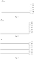
Fig. 1 is a first structural schematic diagram of an OLED light-emitting device provided in an embodiment of the invention; -
Fig. 2 is a second structural schematic diagram of an OLED light-emitting device provided in an embodiment of the invention; -
Fig. 3 is a third structural schematic diagram of an OLED light-emitting device provided in an embodiment of the invention; -
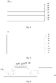
Fig. 4 is a fourth structural schematic diagram of an OLED light-emitting device provided in an embodiment of the invention; -
Fig. 5 is a fifth structural schematic diagram of an OLED light-emitting device provided in an embodiment of the invention; -
Fig. 6 is a structural schematic diagram of a display apparatus provided in an embodiment of the invention; and -
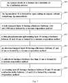
Fig. 7 is a schematic flow chart of a production method for an OLED light-emitting device provided in an embodiment of the invention. - 01 - OLED light-emitting device; 10 - substrate; 20 - anode; 30 - Ag nanolayer; 40 - hole transport layer; 50 - blue phosphorescent light-emitting layer; 60 - cathode; 70 - light-reflecting layer; 80 - covering layer; 90 - electron transport layer; 100 - hole injection layer; 110 - thin film transistor.
- The technical solutions in the embodiments of the invention will be described clearly and fully below in conjunction with accompanying drawings in embodiments of the invention. Obviously, the embodiments described are merely part of the embodiments of the invention, rather than all of the embodiments. Based on the embodiments in the invention, all other embodiments obtained by those of ordinary skill in the art without performing inventive work belong to the scope protected by the invention.
- An embodiment of the invention provides an OLED light-
emitting device 01. As shown inFigs. 1-5 , this OLED light-emitting device 01 comprises asubstrate 10, and ananode 20, ahole transport layer 40, a blue light-emitting layer, and acathode 60 provided on thesubstrate 10, and further comprises anAg nanolayer 30 located between theanode 20 and thehole transport layer 40. - Here, the blue light-emitting layer is a blue phosphorescent light-
emitting layer 50; and the absorption spectrum of theAg nanolayer 30 overlaps the emission spectrum of the blue phosphorescent light-emitting layer 50, and the blue phosphorescent light-emitting layer 50 is located within the penetration depth of surface plasma of Ag nanoparticles in theAg nanolayer 30. - Those to be indicated are as follows. First, since the emission spectrum of the
Ag nanolayer 30 may be adjusted by the size of the Ag nanoparticles in theAg nanolayer 30, the emission spectrum of theAg nanolayer 30 may be allowed to overlap the emission spectrum of the blue phosphorescent light-emittinglayer 50 by adjusting the size of the Ag nanoparticles in the embodiment of the invention. - Here, when phosphorescent materials in the blue phosphorescent light-emitting
layer 50 are different, there is a certain difference in the emission spectra thereof. Therefore, the size of the Ag nanoparticles is not defined in the embodiment of the invention, and the size of the Ag nanoparticles may be correspondingly selected according to the phosphorescent material selected. - Second, the surface plasma is a local surface electromagnetic wave, and has an intensity exhibiting an exponential decay along with the distance vertical to the surface. That is, the surface plasma has a certain effective penetration depth, which is the range of action of surface plasma.
- Here, in the penetration depth

hole transport layer 40 and a part of the blue phosphorescent light-emitting layer 50) contained within the distance between metal surface plasmas and light-emitting excitons (excitons are generated by recombination of holes and electrons in the blue phosphorescent light-emitting layer 50), εm is the dielectric constant of the Ag nanoparticle, and λ is a photoluminescence (simply referred to as PL) spectrum which surface plasma corresponds to, and the unit thereof is nm. - That is, it can be seen from the equation of the penetration depth described above that the value of the penetration depth Z is determined after the materials of the
hole transport layer 40 and the blue phosphorescent light-emitting layer 50 are determined. - On this basis, by adjusting the thickness of the
hole transport layer 40, the blue phosphorescent light-emitting layer 50 is allowed to be located within the penetration depth of surface plasma of the Ag nanoparticles. That is, excitons are limited within the penetration depth of surface plasma of the Ag nanoparticles. - Third, the materials of the
hole transport layer 40 and the blue phosphorescent light-emittinglayer 50 are not defined. - Fourth, the materials of the
anode 20 and thecathode 60 are not defined. Here, thecathode 60 may be allowed to be thinner. That is, thecathode 60 is semi-transparent. Of course, thecathode 60 may also be allowed to be relatively thick. That is, thecathode 60 is opaque. Those may be specifically set according to practical situations, and are not defined herein. - An embodiment of the invention provides an OLED light-
emitting device 01. By forming an Ag nanolayer between theanode 20 and thehole transport layer 40, enabling the absorption spectrum of theAg nanolayer 30 to overlap the emission spectrum of the blue phosphorescent light-emittinglayer 50, and locating the blue phosphorescent light-emittinglayer 50 within the penetration depth of surface plasma of the Ag nanoparticles, resonance between surface plasmas of Ag nanoparticles and excitons formed by recombination on the blue phosphorescent light-emittinglayer 50 is allowed to occur. The energy formed after resonance may be transferred to excitons to perform radioluminescence so as to enhance the speed of spontaneous radiation of triplet excitons and reduce the quenching of triplet-triplet excitons at a high current density, and thus the internal quantum efficiency of the device is increased and the utilization rate of excitons may be increased. - Preferably, the
anode 20 is opaque. That is, a three-layer structure of transparent conductive layer/opaque metal layer/transparent conductive layer, for example a three-layer structure of ITO conductive layer/Ag conductive layer/ITO conductive layer, may be used as theanode 20. Thecathode 60 is semi-transparent. That is, thecathode 60 employs a metal material and has a relatively thin thickness. - Of course, as shown in
Fig. 3 , theanode 20 may also be transparent. That is, an ITO material is used. On this basis, the OLED light-emittingdevice 01 may further comprise a light-reflectinglayer 70 on a side of theanode 20 away from thecathode 60; wherein, with respect to thecathode 60, theanode 20 is provided close to thesubstrate 10. - That is, from bottom to top, there are sequentially: a
substrate 10, a light-reflectinglayer 70, atransparent anode 20, anAg nanolayer 30, ahole transport layer 40, a blue phosphorescent light-emittinglayer 50, and asemi-transparent cathode 60. - Here, the material of the
cathode 60 may be, for example a magnesium silver alloy, and the thickness thereof may be less than 15 nm. - In the embodiment of the invention, illustration is made by exemplifying the
anode 20 which is opaque (i.e., comprising a three-layer structure of transparent conductive layer/opaque metal layer/transparent conductive layer). By allowing theanode 20 to be opaque and allowing thecathode 60 to be semi-transparent, a microcavity may be formed between theanode 20 to thecathode 60. Due to the interference effect (microcavity effect) of the light in the microcavity, the output efficiency of the light may be increased. - Further preferably, as shown in
Fig. 4 , the OLED light-emittingdevice 01 further comprises acovering layer 80 located on a side of thecathode 60 away from thesubstrate 10, and thecovering layer 80 has a refractive index between 1.8 and 2.0. - Here, the thickness of the
covering layer 80 is preferably between 50 and 55 nm. - Since the refractive index of the
covering layer 80 is relatively larger, significant shifts of the intensity and the color coordinate of the light will occur along with the variation of the viewing angle, and the distribution of light intensity substantially complies with Lambertian distribution. That is, the brightness on the vertical angle is much greater than brightnesses on other angles, and thus the output efficiency of the light on the vertical angle may be increased. - Preferably, the Ag nanoparticles have a diameter between 15 and 30 nm, and for example, may be 25 nm.
- Preferably, the Ag nanolayer has a thickness between 15 and 60 nm, preferably between 15 and 30 nm.
- Here, by setting the diameter of the Ag nanoparticles between 15 and 30 nm, the absorption spectrum thereof may be allowed to be at least partly located in the range of the light emission spectrum of the blue phosphorescent light-emitting
layer 50. - Preferably, the
hole transport layer 40 has a thickness between 1100 and 1300 nm. - Here, the material of the
hole transport layer 40 may be aromatic triamine series, biphenyl diamine derivatives, and cross structure linked diamine biphenyl. For example, it may be NPB (N,N'-diphenyl-N,N'-(1-naphthyl)-1,1'-biphenyl-4,4'-diamine), TCTA (4,4',4"-Tri(9-carbazoyl)triphenylamine), m-MTDATA (4,4',4"-Tris (N-3-methylphenyl-N-phenylamino)triphenylamine), or the like. - In the embodiment of the invention, the thickness of the
hole transport layer 40 is set in the range of 1100-1300 nm. On the one hand, surface plasmas of Ag nanoparticles and excitons are separated, and the metallic light absorption due to Forster-type transfer is reduced. On the other hand, projections of theAg nanolayer 30 are completely covered to prevent the phenomenon of breakdown and excitons can be limited within the penetration depth of surface plasma of the Ag nanoparticles, allowing that effective resonance phenomenon can occur between excitons and plasmas. - It is to be indicated that when the OLED light-emitting
device 01 comprises the microcavity structure described above, the thickness of thehole transport layer 40 may be adjusted according to the thickness of the microcavity. - Preferably, the blue phosphorescent light-emitting
layer 50 has a thickness between 20 and 40 nm. - Further, in order to obtain a higher internal quantum efficiency, the blue phosphorescent light-emitting
layer 50 preferably employs a host-guest doping system; wherein an iridium (Ir) complex, for example FIrpic, may be used as a guest material, and CBP (4,4'-Bis(9H-carbazol-9-yl)biphenyl), UGH3 (1,3-bis(triphenylsilicon)benzene), UGH4, mCP (9,9'-(1,3-phenyl)di-9H-carbazole) or the like, may be used as a host material. - In the embodiment of the invention, by setting the thickness of the blue phosphorescent light-emitting
layer 50 in the range of 20-40 nm, it is possible to prevent the light-emitting interface from shifting to an adjacent organic layer. - Preferably, as shown in
Figs. 2-4 , the OLED light-emittingdevice 01 further comprises anelectron transport layer 90 located between thecathode 60 and the blue phosphorescent light-emittinglayer 50. - Here, the material of the
electron transport layer 90 may be metal chelates, azole compounds, phenanthroline derivatives, etc. For example, it may be AlQ3 (tris(8-hydroxyquinolinato)aluminum), BPhen (4,7-diphenyl-1,10-phenanthroline), TmPyPB (1,3,5-tris [(3-pyridyl)-3-phenyl]benzene), OXD-7 (2,2'-(1,3-phenyl)bis [5-(4-tert-butylphenyl)-1,3,4-oxadiazole]). The thickness may be 25-35nm, for example 30 nm. - Compared to one that is not provided with the
electron transport layer 90, it required to enable the blue phosphorescent light-emittinglayer 50 to have a relatively strong ability of electron transport. By providing theelectron transport layer 90, the electron transporting ability may be enhanced, and the requirement for electron transporting ability with respect to the blue phosphorescent light-emittinglayer 50 may be reduced. - Based on those described above, preferably, the OLED light-emitting
device 01 further comprises ahole injection layer 100 located between theanode 20 and thehole transport layer 40. - Here, as shown in
Fig. 5 , theAg nanolayer 30 is located between thehole injection layer 100 and thehole transport layer 40. - Or, the
Ag nanolayer 30 may be located between theanode 20 and thehole injection layer 100. - By providing the
hole injection layer 100, on the one hand, the hole transporting ability may be enhanced, and on the other hand, it may also have a function of repairing surface defects of theanode 20 when it is located above theanode 20 as shown inFig. 5 . - It is to be indicated that since a microcavity is formed between the
anode 20 and thecathode 60 and the thickness of the microcavity is determined, thehole injection layer 100 may have a function of adjusting the thickness of thehole transport layer 40, i.e., a function of adjusting the distance between the plasmas and that excitons, after it is added. - Moreover, with respect to the circumstances as shown in
Fig. 5 , since theAg nanolayer 30 is formed on thehole injection layer 100, an organic solvent which does not corrode thehole injection layer 100 is required to be used when forming theAg nanolayer 30. Here, an aqueous dispersion of poly(3,4-ethylenedioxythiophene) and poly(styrene sulfonates) (PEDOT:PSS) is preferably used as the material for thehole injection layer 100. - An embodiment of the invention further provides a display apparatus, comprising any one of OLED light-emitting
devices 01 described above. - By forming an
Ag nanolayer 30 between theanode 20 and thehole transport layer 40, enabling the absorption spectrum of theAg nanolayer 30 to overlap the emission spectrum of the blue phosphorescent light-emittinglayer 50, and locating the blue phosphorescent light-emittinglayer 50 within the penetration depth of surface plasma of the Ag nanoparticles, resonance between the surface plasmas of Ag nanoparticles and the excitons formed by recombination on the blue phosphorescent light-emittinglayer 50 is allowed to occur. The energy generated after resonance may be transferred to excitons to perform radioluminescence so as to enhance the speed of spontaneous radiation of triplet excitons and reduce the quenching of triplet-triplet excitons at a high current density, and thus the internal quantum efficiency of the device is increased and the utilization rate of excitons may be increased. - In view of the deficient aspect of a passive matrix when being used in a large-size display apparatus, it is preferable that the display apparatus provided in an embodiment of the invention is an active matrix type display apparatus. That is, as shown in
Fig. 6 , the display apparatus further comprises athin film transistor 110 electrically connected to ananode 20 of the OLED light-emittingdevice 01. - Here, the
thin film transistor 110 comprises a gate electrode, a gate insulating layer, a semiconductor active layer, a source electrode, and a drain electrode. - It is to be indicated that the structure of the
thin film transistor 110 is not defined in the embodiment of the invention, and it may be top gate type or may be bottom gate type. Moreover, the material of the semiconductor active layer is not defined either, and it may employ semiconductor materials, such as amorphous silicon, polycrystalline silicon, metal oxides, organic materials or the like. - Of course, the OLED display apparatus should further comprise a package substrate overlying on the
cathode 60 or thecovering layer 80. The package substrate may be a thin film or may be a glass cover plate, and it is not specifically defined herein. - An embodiment of the invention further provides a production method for an OLED light-emitting device, and with reference to those shown in
Fig. 1 , this production method comprises: forming ananode 20, ahole transport layer 40, a blue light-emitting layer, and acathode 60 on asubstrate 10; and the method further comprises: forming anAg nanolayer 30 between theanode 20 and thehole transport layer 40. Here, the blue light-emitting layer is a blue phosphorescent light-emittinglayer 50; and the absorption spectrum of theAg nanolayer 30 overlaps the emission spectrum of the blue phosphorescent light-emittinglayer 50, and the blue phosphorescent light-emittinglayer 50 is located within the penetration depth of surface plasma of the Ag nanoparticles in theAg nanolayer 30. - Here, spin-coating an organic solvent containing the Ag nanoparticle may be used to form an
Ag nanolayer 30, or thermal evaporation may be used to evaporate a metal thin layer and then annealing treatment is performed to agglomerate the metal thin film into nanoparticles so as to form anAg nanolayer 30, and it is not specifically defined herein. - Preferably, the
anode 20 is opaque and thecathode 60 is semi-transparent. - Here, a three-layer structure of ITO conductive layer/Ag conductive layer/ITO conductive layer may be used as the
anode 20. The material of thecathode 60 may be, for example a magnesium silver alloy, and the thickness thereof may be less than 15 nm. - Further preferably, with reference to those shown in
Fig. 4 , the method further comprises forming acovering layer 80 on a side of thecathode 60 away from thesubstrate 10, and thecovering layer 80 has a refractive index between 1.8 and 2.0. Here, the thickness of thecovering layer 80 is preferably between 50 and 55 nm. - Preferably, Ag nanoparticles having a diameter of 15-30 nm may be synthesized by a Liquid-Solid-Solution (simply referred to as LSS) chemical synthesis method. Thus, the absorption spectrum thereof may be allowed to be at least partly located in the range of the light emission spectrum of the blue phosphorescent light-emitting
layer 50. - On this basis, the
Ag nanolayer 30 may be formed by spin-coating an organic solvent containing Ag nanoparticles. - Preferably, the
hole transport layer 40 having a thickness between 1100 and 1300 nm is formed by an evaporation method. - Here, the material of the
hole transport layer 40 may be aromatic triamine series, biphenyl diamine derivatives, cross structure linked diamine biphenyl, or the like. - In the embodiment of the invention, the
hole transport layer 40 having a thickness of 1100-1300 nm is formed. On the one hand, the surface plasmas of Ag nanoparticles and excitons are separated, and the metallic light absorption due to Forster-type transfer is reduced. On the other hand, the projections of theAg nanolayer 30 are completely covered to prevent the phenomenon of breakdown and excitons can be limited within the penetration depth of surface plasma of the Ag nanoparticle, allowing that effective resonance phenomenon can occur between excitons and plasmas. - Preferably, the blue phosphorescent light-emitting
layer 50 having a thickness between 20 and 40 nm is formed by an evaporation method. In order to obtain a higher internal quantum efficiency, the blue phosphorescent light-emittinglayer 50 preferably employs a host-guest doping system; wherein an iridium (Ir) complex, for example FIrpic, may be used as a guest material, and CBP, UGH3, UGH4, mCP or the like, may be used as a host material. - Preferably, as shown in
Figs. 2-5 , the method further comprises forming anelectron transport layer 90 having a thickness between 25 and 35 nm by an evaporation method. Here, the material of theelectron transport layer 90 may be metal chelates, azole compounds, phenanthroline derivatives, or the like. - Based on those described above, preferably, with reference to those shown in
Fig. 5 , the method further comprises forming ahole injection layer 100 between theanode 20 and theAg nanolayer 30 by an evaporation method. Here, an aqueous dispersion of poly(3,4-ethylenedioxythiophene) and poly(styrene sulfonates) (PEDOT:PSS) is preferably used as the material for thehole injection layer 100. - Moreover, the
hole injection layer 100 may also be formed between theAg nanolayer 30 and thehole transport layer 40. - A specific example is provided below to describe a production method for an OLED light-emitting
device 01 in detail. As shown inFig. 7 , this method comprises the following steps. - S10: With reference to those shown in
Fig. 4 , anopaque anode 20 is formed on asubstrate 10 by a patterning process. - For example, a three-layer structure of ITO conductive layer/Ag conductive layer/ITO conductive layer is used as the
anode 20. - S11: With reference to those shown in
Fig. 4 , on the basis of S10, anAg nanolayer 30 is formed by spin-coating an organic solvent comprising Ag nanoparticles. - Here, an Ag nanoparticle having a diameter of 15-30 nm may be synthesized by using a Liquid-Solid-Solution chemical synthesis method.
- S12: With reference to those shown in
Fig. 4 , on the basis of S11, ahole transport layer 40 having a thickness between 1100 and 1300 nm is formed by a vacuum evaporation method. - Here, the material of the
hole transport layer 40 may be NPB, TCTA, m-MTDATA, etc. - S13: With reference to those shown in
Fig. 4 , on the basis of S12, a blue phosphorescent light-emittinglayer 50 having a thickness between 20 and 40 nm is formed by a vacuum evaporation method. - Here, in the blue phosphorescent light-emitting
layer 50, FIrpi may be used as a guest material, and CBP, UGH3, UGH4, mCP, etc., may be used as a host material. - S14: With reference to those shown in
Fig. 4 , on the basis of S13, anelectron transport layer 90 having a thickness between 25 and 35 nm is formed by a vacuum evaporation method. - Here, the material of the
electron transport layer 90 may be AlQ3, BPhen, TmPyPB, OXD-7, or the like. - S15: With reference to those shown in
Fig. 4 , on the basis of S14, acathode 60 having a thickness less than 15 nm is formed by a vacuum evaporation method. - Here, the material of the
cathode 60 may be a magnesium silver alloy. - S16: With reference to those shown in
Fig. 4 , on the basis of S15, acovering layer 80 having a thickness between 50 and 55 nm and a refractive index between 1.8 and 2.0 is formed by a vacuum evaporation method. - Those described above are only specific embodiments of the invention, but the scope of the invention is not limited thereto. Within the technical scope disclosed by this present invention, any person skilled in the art will easily conceive variations or replacements, which should be covered by the scope of the invention. Therefore, the protection scope of the invention should be determined by the scope of the claims.
Claims (16)
- An OLED light-emitting device, comprising a substrate, and an anode, a hole transport layer, a blue light-emitting layer and a cathode provided on the substrate; characterized in that:the OLED light-emitting device further comprises an Ag nanolayer located between the anode and the hole transport layer;wherein the blue light-emitting layer is a blue phosphorescent light-emitting layer;the absorption spectrum of the Ag nanolayer overlaps the emission spectrum of the blue phosphorescent light-emitting layer, and the blue phosphorescent light-emitting layer is located within the penetration depth of surface plasma of Ag nanoparticles in the Ag nanolayer.
- The OLED light-emitting device according to claim 1, characterized in that:the anode is opaque, and the cathode is semi-transparent.
- The OLED light-emitting device according to claim 2, characterized in that:the OLED light-emitting device further comprises a covering layer located on a side of the cathode away from the substrate, wherein the covering layer has a refractive index between 1.8 and 2.0.
- The OLED light-emitting device according to claim 1, characterized in that:the Ag nanoparticles have a diameter between 15 and 30 nm.
- The OLED light-emitting device according to claim 1, characterized in that:the Ag nanolayer has a thickness between 15 and 60 nm.
- The OLED light-emitting device according to claim 1, characterized in that:the hole transport layer has a thickness between 1100 and 1300 nm.
- The OLED light-emitting device according to claim 1, characterized in that:the blue phosphorescent light-emitting layer has a thickness between 20 and 40 nm.
- The OLED light-emitting device according to claim 1, characterized in that:the OLED light-emitting device further comprises an electron transport layer located between the cathode and the blue phosphorescent light-emitting layer.
- The OLED light-emitting device according to any one of claims 1 to 8, characterized in that:the OLED light-emitting device further comprises a hole injection layer located between the anode and the hole transport layer;wherein the Ag nanolayer is located between the hole injection layer and the hole transport layer, or the Ag nanolayer is located between the anode and the hole injection layer.
- A display apparatus, characterized by comprising the OLED light-emitting device of any one of claims 1 to 9.
- The display apparatus according to claim 10, characterized in that the display apparatus further comprises a thin film transistor electrically connected to the anode of the OLED light-emitting device.
- A production method for an OLED light-emitting device, comprising forming an anode, a hole transport layer, a blue light-emitting layer, and a cathode on a substrate; characterized in that the method further comprises forming an Ag nanolayer between the anode and the hole transport layer;
wherein the blue light-emitting layer is a blue phosphorescent light-emitting layer;
the absorption spectrum of the Ag nanolayer overlaps the emission spectrum of the blue phosphorescent light-emitting layer, and the blue phosphorescent light-emitting layer is located within the penetration depth of surface plasma of Ag nanoparticles in the Ag nanolayer. - The method according to claim 12, characterized in that:Ag nanoparticles having a diameter of 15-30 nm are synthesized by a Liquid-Solid-Solution chemical synthesis method; andthe Ag nanolayer is formed by spin-coating an organic solvent comprising the Ag nanoparticles.
- The method according to claim 12, characterized in that:the Ag nanolayer has a thickness between 15 and 60 nm.
- The method according to claim 12, characterized in that:the hole transport layer, which has a thickness between 1100 and 1300 nm, is formed by an evaporation method.
- The method according to any one of claims 12 to 15, characterized in that:the anode is opaque, and the cathode is semi-transparent.
Applications Claiming Priority (2)
| Application Number | Priority Date | Filing Date | Title |
|---|---|---|---|
| CN201510472870.3A CN104993065B (en) | 2015-08-04 | 2015-08-04 | A kind of OLED luminescent devices and preparation method thereof, display device |
| PCT/CN2015/097272 WO2017020475A1 (en) | 2015-08-04 | 2015-12-14 | Oled light-emitting device, preparation method therefor and display device |
Publications (3)
| Publication Number | Publication Date |
|---|---|
| EP3168890A1 true EP3168890A1 (en) | 2017-05-17 |
| EP3168890A4 EP3168890A4 (en) | 2018-04-04 |
| EP3168890B1 EP3168890B1 (en) | 2019-03-06 |
Family
ID=54304847
Family Applications (1)
| Application Number | Title | Priority Date | Filing Date |
|---|---|---|---|
| EP15891407.7A Not-in-force EP3168890B1 (en) | 2015-08-04 | 2015-12-14 | Oled light-emitting device, preparation method therefor and display device |
Country Status (4)
| Country | Link |
|---|---|
| US (1) | US10566579B2 (en) |
| EP (1) | EP3168890B1 (en) |
| CN (1) | CN104993065B (en) |
| WO (1) | WO2017020475A1 (en) |
Cited By (4)
| Publication number | Priority date | Publication date | Assignee | Title |
|---|---|---|---|---|
| EP3709378A1 (en) * | 2019-03-12 | 2020-09-16 | Universal Display Corporation | Nanopatch antenna outcoupling structure for use in oleds |
| US11569480B2 (en) | 2019-03-12 | 2023-01-31 | Universal Display Corporation | Plasmonic OLEDs and vertical dipole emitters |
| US11637261B2 (en) | 2019-03-12 | 2023-04-25 | Universal Display Corporation | Nanopatch antenna outcoupling structure for use in OLEDs |
| US12414433B2 (en) | 2022-02-11 | 2025-09-09 | Universal Display Corporation | Organic electroluminescent devices |
Families Citing this family (17)
| Publication number | Priority date | Publication date | Assignee | Title |
|---|---|---|---|---|
| CN104993065B (en) | 2015-08-04 | 2018-04-27 | 京东方科技集团股份有限公司 | A kind of OLED luminescent devices and preparation method thereof, display device |
| CN106450016B (en) * | 2016-10-17 | 2019-11-12 | Tcl集团股份有限公司 | A kind of luminescent device and preparation method |
| CN106784348A (en) * | 2016-12-15 | 2017-05-31 | Tcl集团股份有限公司 | QLED containing noble metal nanometer material and preparation method thereof |
| CN107230747A (en) * | 2017-05-27 | 2017-10-03 | 深圳市华星光电技术有限公司 | The preparation method and OLED display panel of OLED display panel |
| US10505154B2 (en) | 2017-05-27 | 2019-12-10 | Shenzhen China Star Optoelectronics Technology Co., Ltd. | Manufacturing method of organic light emitting diode display panel and organic light emitting diode display panel |
| CN107994131A (en) * | 2017-11-28 | 2018-05-04 | 武汉华星光电半导体显示技术有限公司 | For encapsulating encapsulating structure, the display device of OLED device |
| US11145692B2 (en) | 2017-12-12 | 2021-10-12 | Universal Display Corporation | Hybrid wearable organic light emitting diode (OLED) illumination devices |
| US11139444B2 (en) | 2017-12-12 | 2021-10-05 | Universal Display Corporation | Organic electroluminescent devices containing a near-infrared down-conversion layer |
| CN108172694B (en) * | 2017-12-21 | 2020-01-14 | 昆山维信诺科技有限公司 | Display panel and display device |
| US11690285B2 (en) | 2018-11-28 | 2023-06-27 | Universal Display Corporation | Electroluminescent devices |
| CN110161600B (en) * | 2019-07-09 | 2022-08-30 | 京东方科技集团股份有限公司 | Array substrate, preparation method thereof and liquid crystal display device |
| CN118647224A (en) * | 2019-11-14 | 2024-09-13 | 环球展览公司 | Host materials for electroluminescent devices |
| CN111816792B (en) * | 2020-08-18 | 2025-01-17 | 京东方科技集团股份有限公司 | Light emitting device and display apparatus |
| CN112952025A (en) * | 2021-03-31 | 2021-06-11 | 京东方科技集团股份有限公司 | Display substrate and display device |
| CN113410410B (en) * | 2021-06-15 | 2022-11-25 | 安徽熙泰智能科技有限公司 | Device for improving luminous efficiency of silicon-based OLED and preparation method thereof |
| US20240357855A1 (en) * | 2022-04-24 | 2024-10-24 | Beijing Boe Technology Development Co., Ltd. | Quantum dot light emitting diode, manufacturing method thereof and display panel |
| CN119297741A (en) * | 2024-10-10 | 2025-01-10 | 安徽格恩半导体有限公司 | A gallium nitride-based compound semiconductor laser chip |
Family Cites Families (11)
| Publication number | Priority date | Publication date | Assignee | Title |
|---|---|---|---|---|
| US123303A (en) * | 1872-01-30 | stewart | ||
| TW587239B (en) * | 1999-11-30 | 2004-05-11 | Semiconductor Energy Lab | Electric device |
| TW543344B (en) * | 2002-10-25 | 2003-07-21 | Ritdisplay Corp | Organic light emitting diode and organic emitting material thereof |
| US20070222371A1 (en) * | 2006-03-21 | 2007-09-27 | Eastman Kodak Company | Top-emitting OLED device with improved stability |
| JP2008243669A (en) * | 2007-03-28 | 2008-10-09 | Toyota Central R&D Labs Inc | Organic electroluminescence device |
| CN101132055A (en) * | 2007-09-28 | 2008-02-27 | 天津理工大学 | A device capable of improving the brightness and efficiency of an organic electroluminescence device and its preparation method |
| JP5312146B2 (en) | 2009-03-30 | 2013-10-09 | ユー・ディー・シー アイルランド リミテッド | Light emitting element |
| JP5306038B2 (en) | 2009-04-24 | 2013-10-02 | ユー・ディー・シー アイルランド リミテッド | Organic electroluminescence device |
| CN102820433B (en) | 2012-08-31 | 2016-05-25 | 昆山工研院新型平板显示技术中心有限公司 | The anti-reflection structure of OLED |
| CN104600205A (en) * | 2015-01-09 | 2015-05-06 | 上海大学 | Metal plasma color conversion enhanced WOLED (white organic light emitting diode) illuminating device and preparation method thereof |
| CN104993065B (en) | 2015-08-04 | 2018-04-27 | 京东方科技集团股份有限公司 | A kind of OLED luminescent devices and preparation method thereof, display device |
-
2015
- 2015-08-04 CN CN201510472870.3A patent/CN104993065B/en active Active
- 2015-12-14 US US15/321,576 patent/US10566579B2/en active Active
- 2015-12-14 WO PCT/CN2015/097272 patent/WO2017020475A1/en not_active Ceased
- 2015-12-14 EP EP15891407.7A patent/EP3168890B1/en not_active Not-in-force
Cited By (9)
| Publication number | Priority date | Publication date | Assignee | Title |
|---|---|---|---|---|
| EP3709378A1 (en) * | 2019-03-12 | 2020-09-16 | Universal Display Corporation | Nanopatch antenna outcoupling structure for use in oleds |
| US11139442B2 (en) | 2019-03-12 | 2021-10-05 | Universal Display Corporation | Nanopatch antenna outcoupling structure for use in OLEDs |
| US11569480B2 (en) | 2019-03-12 | 2023-01-31 | Universal Display Corporation | Plasmonic OLEDs and vertical dipole emitters |
| US11637261B2 (en) | 2019-03-12 | 2023-04-25 | Universal Display Corporation | Nanopatch antenna outcoupling structure for use in OLEDs |
| US11963389B2 (en) | 2019-03-12 | 2024-04-16 | Universal Display Corporation | Plasmonic OLEDs and vertical dipole emitters |
| US11968851B2 (en) | 2019-03-12 | 2024-04-23 | Universal Display Corporation | Organic electroluminescent devices |
| US12225760B2 (en) | 2019-03-12 | 2025-02-11 | Universal Display Corporation | Organic electroluminescent devices |
| US12232348B2 (en) | 2019-03-12 | 2025-02-18 | Universal Display Corporation | Organic electroluminescent devices |
| US12414433B2 (en) | 2022-02-11 | 2025-09-09 | Universal Display Corporation | Organic electroluminescent devices |
Also Published As
| Publication number | Publication date |
|---|---|
| WO2017020475A1 (en) | 2017-02-09 |
| EP3168890B1 (en) | 2019-03-06 |
| US10566579B2 (en) | 2020-02-18 |
| EP3168890A4 (en) | 2018-04-04 |
| CN104993065A (en) | 2015-10-21 |
| CN104993065B (en) | 2018-04-27 |
| US20180212201A1 (en) | 2018-07-26 |
Similar Documents
| Publication | Publication Date | Title |
|---|---|---|
| EP3168890B1 (en) | Oled light-emitting device, preparation method therefor and display device | |
| KR101453874B1 (en) | White organic light emitting device | |
| CN109786568B (en) | Organic light emitting diode and organic light emitting display device including same | |
| CN102272972B (en) | Radiation-emitting device | |
| US8552639B2 (en) | White organic light emitting device | |
| KR102761413B1 (en) | Organic light emitting device | |
| US10826021B2 (en) | Organic electroluminescence device including a plurality of unit regions each including a light emitting area and a transmissive area | |
| TW201208167A (en) | Electroluminescent devices for lighting applications | |
| KR101581033B1 (en) | organic light-emitting diode, and display device and illumination | |
| JP2017535083A (en) | Organic light emitting diode display device and manufacturing method thereof | |
| KR102083985B1 (en) | Organic light emitting diode and method for preparing the same | |
| Lu et al. | Solution-processable tandem solid-state light-emitting electrochemical cells | |
| Park et al. | Optical design and optimization of highly efficient sunlight-like three-stacked warm white organic light emitting diodes | |
| EP2874471B1 (en) | Organic electroluminescent element | |
| EP3451401B1 (en) | Oled device and method for manufacturing same, and oled display panel | |
| CN106531897B (en) | A kind of organic electroluminescence device and preparation method thereof based on exciplex | |
| Chen et al. | Efficient, color-stable flexible white top-emitting organic light-emitting diodes | |
| Lee | Phosphorescent white organic light-emitting diodes with stable white color depending on luminance | |
| KR102372275B1 (en) | Organic Light Emitting Device and Method of manufacturing the same and Organic Light Emitting Display Device using the same | |
| KR102349697B1 (en) | Organic Light Emitting Device and Method of manufacturing the same and Organic Light Emitting Display Device using the same | |
| KR102080044B1 (en) | Organic Light Emitting Device and Method of manufacturing the same | |
| Shi et al. | High-performance green phosphorescent top-emitting organic light-emitting diodes based on FDTD optical simulation | |
| KR20160082551A (en) | Organic Light Emitting Device and Method of manufacturing the same and Organic Light Emitting Display Device using the same | |
| Rai et al. | White organic electroluminescence from fluorescent bis (2-(2-hydroxyphenyl) benzoxazolate) zinc doped with phosphorescent material | |
| Wang et al. | An efficient dual-emissive-layer white organic light emitting-diode: Insight into device working mechanism and origin of color-shift |
Legal Events
| Date | Code | Title | Description |
|---|---|---|---|
| STAA | Information on the status of an ep patent application or granted ep patent |
Free format text: STATUS: UNKNOWN |
|
| STAA | Information on the status of an ep patent application or granted ep patent |
Free format text: STATUS: THE INTERNATIONAL PUBLICATION HAS BEEN MADE |
|
| PUAI | Public reference made under article 153(3) epc to a published international application that has entered the european phase |
Free format text: ORIGINAL CODE: 0009012 |
|
| STAA | Information on the status of an ep patent application or granted ep patent |
Free format text: STATUS: REQUEST FOR EXAMINATION WAS MADE |
|
| 17P | Request for examination filed |
Effective date: 20161114 |
|
| AK | Designated contracting states |
Kind code of ref document: A1 Designated state(s): AL AT BE BG CH CY CZ DE DK EE ES FI FR GB GR HR HU IE IS IT LI LT LU LV MC MK MT NL NO PL PT RO RS SE SI SK SM TR |
|
| AX | Request for extension of the european patent |
Extension state: BA ME |
|
| R17P | Request for examination filed (corrected) |
Effective date: 20161114 |
|
| A4 | Supplementary search report drawn up and despatched |
Effective date: 20180305 |
|
| RIC1 | Information provided on ipc code assigned before grant |
Ipc: H01L 51/56 20060101ALI20180226BHEP Ipc: H01L 51/52 20060101ALI20180226BHEP Ipc: H01L 27/32 20060101ALI20180226BHEP Ipc: H01L 51/50 20060101AFI20180226BHEP |
|
| GRAP | Despatch of communication of intention to grant a patent |
Free format text: ORIGINAL CODE: EPIDOSNIGR1 |
|
| STAA | Information on the status of an ep patent application or granted ep patent |
Free format text: STATUS: GRANT OF PATENT IS INTENDED |
|
| RIC1 | Information provided on ipc code assigned before grant |
Ipc: H01L 51/50 20060101AFI20180921BHEP Ipc: H01L 51/52 20060101ALI20180921BHEP |
|
| DAV | Request for validation of the european patent (deleted) | ||
| DAX | Request for extension of the european patent (deleted) | ||
| INTG | Intention to grant announced |
Effective date: 20181016 |
|
| GRAS | Grant fee paid |
Free format text: ORIGINAL CODE: EPIDOSNIGR3 |
|
| GRAA | (expected) grant |
Free format text: ORIGINAL CODE: 0009210 |
|
| STAA | Information on the status of an ep patent application or granted ep patent |
Free format text: STATUS: THE PATENT HAS BEEN GRANTED |
|
| AK | Designated contracting states |
Kind code of ref document: B1 Designated state(s): AL AT BE BG CH CY CZ DE DK EE ES FI FR GB GR HR HU IE IS IT LI LT LU LV MC MK MT NL NO PL PT RO RS SE SI SK SM TR |
|
| REG | Reference to a national code |
Ref country code: GB Ref legal event code: FG4D |
|
| REG | Reference to a national code |
Ref country code: CH Ref legal event code: EP Ref country code: AT Ref legal event code: REF Ref document number: 1105735 Country of ref document: AT Kind code of ref document: T Effective date: 20190315 |
|
| REG | Reference to a national code |
Ref country code: DE Ref legal event code: R096 Ref document number: 602015026129 Country of ref document: DE |
|
| REG | Reference to a national code |
Ref country code: IE Ref legal event code: FG4D |
|
| REG | Reference to a national code |
Ref country code: NL Ref legal event code: FP |
|
| REG | Reference to a national code |
Ref country code: LT Ref legal event code: MG4D |
|
| PG25 | Lapsed in a contracting state [announced via postgrant information from national office to epo] |
Ref country code: FI Free format text: LAPSE BECAUSE OF FAILURE TO SUBMIT A TRANSLATION OF THE DESCRIPTION OR TO PAY THE FEE WITHIN THE PRESCRIBED TIME-LIMIT Effective date: 20190306 Ref country code: SE Free format text: LAPSE BECAUSE OF FAILURE TO SUBMIT A TRANSLATION OF THE DESCRIPTION OR TO PAY THE FEE WITHIN THE PRESCRIBED TIME-LIMIT Effective date: 20190306 Ref country code: NO Free format text: LAPSE BECAUSE OF FAILURE TO SUBMIT A TRANSLATION OF THE DESCRIPTION OR TO PAY THE FEE WITHIN THE PRESCRIBED TIME-LIMIT Effective date: 20190606 Ref country code: LT Free format text: LAPSE BECAUSE OF FAILURE TO SUBMIT A TRANSLATION OF THE DESCRIPTION OR TO PAY THE FEE WITHIN THE PRESCRIBED TIME-LIMIT Effective date: 20190306 |
|
| PG25 | Lapsed in a contracting state [announced via postgrant information from national office to epo] |
Ref country code: GR Free format text: LAPSE BECAUSE OF FAILURE TO SUBMIT A TRANSLATION OF THE DESCRIPTION OR TO PAY THE FEE WITHIN THE PRESCRIBED TIME-LIMIT Effective date: 20190607 Ref country code: RS Free format text: LAPSE BECAUSE OF FAILURE TO SUBMIT A TRANSLATION OF THE DESCRIPTION OR TO PAY THE FEE WITHIN THE PRESCRIBED TIME-LIMIT Effective date: 20190306 Ref country code: HR Free format text: LAPSE BECAUSE OF FAILURE TO SUBMIT A TRANSLATION OF THE DESCRIPTION OR TO PAY THE FEE WITHIN THE PRESCRIBED TIME-LIMIT Effective date: 20190306 Ref country code: BG Free format text: LAPSE BECAUSE OF FAILURE TO SUBMIT A TRANSLATION OF THE DESCRIPTION OR TO PAY THE FEE WITHIN THE PRESCRIBED TIME-LIMIT Effective date: 20190606 Ref country code: LV Free format text: LAPSE BECAUSE OF FAILURE TO SUBMIT A TRANSLATION OF THE DESCRIPTION OR TO PAY THE FEE WITHIN THE PRESCRIBED TIME-LIMIT Effective date: 20190306 |
|
| REG | Reference to a national code |
Ref country code: AT Ref legal event code: MK05 Ref document number: 1105735 Country of ref document: AT Kind code of ref document: T Effective date: 20190306 |
|
| PG25 | Lapsed in a contracting state [announced via postgrant information from national office to epo] |
Ref country code: RO Free format text: LAPSE BECAUSE OF FAILURE TO SUBMIT A TRANSLATION OF THE DESCRIPTION OR TO PAY THE FEE WITHIN THE PRESCRIBED TIME-LIMIT Effective date: 20190306 Ref country code: SK Free format text: LAPSE BECAUSE OF FAILURE TO SUBMIT A TRANSLATION OF THE DESCRIPTION OR TO PAY THE FEE WITHIN THE PRESCRIBED TIME-LIMIT Effective date: 20190306 Ref country code: EE Free format text: LAPSE BECAUSE OF FAILURE TO SUBMIT A TRANSLATION OF THE DESCRIPTION OR TO PAY THE FEE WITHIN THE PRESCRIBED TIME-LIMIT Effective date: 20190306 Ref country code: IT Free format text: LAPSE BECAUSE OF FAILURE TO SUBMIT A TRANSLATION OF THE DESCRIPTION OR TO PAY THE FEE WITHIN THE PRESCRIBED TIME-LIMIT Effective date: 20190306 Ref country code: AL Free format text: LAPSE BECAUSE OF FAILURE TO SUBMIT A TRANSLATION OF THE DESCRIPTION OR TO PAY THE FEE WITHIN THE PRESCRIBED TIME-LIMIT Effective date: 20190306 Ref country code: ES Free format text: LAPSE BECAUSE OF FAILURE TO SUBMIT A TRANSLATION OF THE DESCRIPTION OR TO PAY THE FEE WITHIN THE PRESCRIBED TIME-LIMIT Effective date: 20190306 Ref country code: PT Free format text: LAPSE BECAUSE OF FAILURE TO SUBMIT A TRANSLATION OF THE DESCRIPTION OR TO PAY THE FEE WITHIN THE PRESCRIBED TIME-LIMIT Effective date: 20190706 Ref country code: CZ Free format text: LAPSE BECAUSE OF FAILURE TO SUBMIT A TRANSLATION OF THE DESCRIPTION OR TO PAY THE FEE WITHIN THE PRESCRIBED TIME-LIMIT Effective date: 20190306 |
|
| PG25 | Lapsed in a contracting state [announced via postgrant information from national office to epo] |
Ref country code: SM Free format text: LAPSE BECAUSE OF FAILURE TO SUBMIT A TRANSLATION OF THE DESCRIPTION OR TO PAY THE FEE WITHIN THE PRESCRIBED TIME-LIMIT Effective date: 20190306 Ref country code: PL Free format text: LAPSE BECAUSE OF FAILURE TO SUBMIT A TRANSLATION OF THE DESCRIPTION OR TO PAY THE FEE WITHIN THE PRESCRIBED TIME-LIMIT Effective date: 20190306 |
|
| REG | Reference to a national code |
Ref country code: DE Ref legal event code: R097 Ref document number: 602015026129 Country of ref document: DE |
|
| PG25 | Lapsed in a contracting state [announced via postgrant information from national office to epo] |
Ref country code: AT Free format text: LAPSE BECAUSE OF FAILURE TO SUBMIT A TRANSLATION OF THE DESCRIPTION OR TO PAY THE FEE WITHIN THE PRESCRIBED TIME-LIMIT Effective date: 20190306 Ref country code: IS Free format text: LAPSE BECAUSE OF FAILURE TO SUBMIT A TRANSLATION OF THE DESCRIPTION OR TO PAY THE FEE WITHIN THE PRESCRIBED TIME-LIMIT Effective date: 20190706 |
|
| PLBE | No opposition filed within time limit |
Free format text: ORIGINAL CODE: 0009261 |
|
| STAA | Information on the status of an ep patent application or granted ep patent |
Free format text: STATUS: NO OPPOSITION FILED WITHIN TIME LIMIT |
|
| PG25 | Lapsed in a contracting state [announced via postgrant information from national office to epo] |
Ref country code: DK Free format text: LAPSE BECAUSE OF FAILURE TO SUBMIT A TRANSLATION OF THE DESCRIPTION OR TO PAY THE FEE WITHIN THE PRESCRIBED TIME-LIMIT Effective date: 20190306 |
|
| 26N | No opposition filed |
Effective date: 20191209 |
|
| PG25 | Lapsed in a contracting state [announced via postgrant information from national office to epo] |
Ref country code: SI Free format text: LAPSE BECAUSE OF FAILURE TO SUBMIT A TRANSLATION OF THE DESCRIPTION OR TO PAY THE FEE WITHIN THE PRESCRIBED TIME-LIMIT Effective date: 20190306 |
|
| PG25 | Lapsed in a contracting state [announced via postgrant information from national office to epo] |
Ref country code: TR Free format text: LAPSE BECAUSE OF FAILURE TO SUBMIT A TRANSLATION OF THE DESCRIPTION OR TO PAY THE FEE WITHIN THE PRESCRIBED TIME-LIMIT Effective date: 20190306 |
|
| REG | Reference to a national code |
Ref country code: CH Ref legal event code: PL |
|
| REG | Reference to a national code |
Ref country code: BE Ref legal event code: MM Effective date: 20191231 |
|
| PG25 | Lapsed in a contracting state [announced via postgrant information from national office to epo] |
Ref country code: MC Free format text: LAPSE BECAUSE OF FAILURE TO SUBMIT A TRANSLATION OF THE DESCRIPTION OR TO PAY THE FEE WITHIN THE PRESCRIBED TIME-LIMIT Effective date: 20190306 |
|
| PG25 | Lapsed in a contracting state [announced via postgrant information from national office to epo] |
Ref country code: LU Free format text: LAPSE BECAUSE OF NON-PAYMENT OF DUE FEES Effective date: 20191214 Ref country code: IE Free format text: LAPSE BECAUSE OF NON-PAYMENT OF DUE FEES Effective date: 20191214 |
|
| PG25 | Lapsed in a contracting state [announced via postgrant information from national office to epo] |
Ref country code: LI Free format text: LAPSE BECAUSE OF NON-PAYMENT OF DUE FEES Effective date: 20191231 Ref country code: CH Free format text: LAPSE BECAUSE OF NON-PAYMENT OF DUE FEES Effective date: 20191231 Ref country code: BE Free format text: LAPSE BECAUSE OF NON-PAYMENT OF DUE FEES Effective date: 20191231 |
|
| PG25 | Lapsed in a contracting state [announced via postgrant information from national office to epo] |
Ref country code: CY Free format text: LAPSE BECAUSE OF FAILURE TO SUBMIT A TRANSLATION OF THE DESCRIPTION OR TO PAY THE FEE WITHIN THE PRESCRIBED TIME-LIMIT Effective date: 20190306 |
|
| PG25 | Lapsed in a contracting state [announced via postgrant information from national office to epo] |
Ref country code: HU Free format text: LAPSE BECAUSE OF FAILURE TO SUBMIT A TRANSLATION OF THE DESCRIPTION OR TO PAY THE FEE WITHIN THE PRESCRIBED TIME-LIMIT; INVALID AB INITIO Effective date: 20151214 Ref country code: MT Free format text: LAPSE BECAUSE OF FAILURE TO SUBMIT A TRANSLATION OF THE DESCRIPTION OR TO PAY THE FEE WITHIN THE PRESCRIBED TIME-LIMIT Effective date: 20190306 |
|
| PG25 | Lapsed in a contracting state [announced via postgrant information from national office to epo] |
Ref country code: MK Free format text: LAPSE BECAUSE OF FAILURE TO SUBMIT A TRANSLATION OF THE DESCRIPTION OR TO PAY THE FEE WITHIN THE PRESCRIBED TIME-LIMIT Effective date: 20190306 |
|
| REG | Reference to a national code |
Ref country code: DE Ref legal event code: R079 Ref document number: 602015026129 Country of ref document: DE Free format text: PREVIOUS MAIN CLASS: H01L0051500000 Ipc: H10K0050000000 |
|
| PGFP | Annual fee paid to national office [announced via postgrant information from national office to epo] |
Ref country code: GB Payment date: 20231220 Year of fee payment: 9 |
|
| PGFP | Annual fee paid to national office [announced via postgrant information from national office to epo] |
Ref country code: NL Payment date: 20231220 Year of fee payment: 9 Ref country code: FR Payment date: 20231221 Year of fee payment: 9 Ref country code: DE Payment date: 20231017 Year of fee payment: 9 |
|
| REG | Reference to a national code |
Ref country code: DE Ref legal event code: R119 Ref document number: 602015026129 Country of ref document: DE |
|
| REG | Reference to a national code |
Ref country code: NL Ref legal event code: MM Effective date: 20250101 |
|
| GBPC | Gb: european patent ceased through non-payment of renewal fee |
Effective date: 20241214 |
|
| PG25 | Lapsed in a contracting state [announced via postgrant information from national office to epo] |
Ref country code: NL Free format text: LAPSE BECAUSE OF NON-PAYMENT OF DUE FEES Effective date: 20250101 |
|
| PG25 | Lapsed in a contracting state [announced via postgrant information from national office to epo] |
Ref country code: DE Free format text: LAPSE BECAUSE OF NON-PAYMENT OF DUE FEES Effective date: 20250701 |
|
| PG25 | Lapsed in a contracting state [announced via postgrant information from national office to epo] |
Ref country code: GB Free format text: LAPSE BECAUSE OF NON-PAYMENT OF DUE FEES Effective date: 20241214 |
|
| PG25 | Lapsed in a contracting state [announced via postgrant information from national office to epo] |
Ref country code: FR Free format text: LAPSE BECAUSE OF NON-PAYMENT OF DUE FEES Effective date: 20241231 |