EP3168877A1 - A wire shaped coaxial photovoltaic solar cell - Google Patents
A wire shaped coaxial photovoltaic solar cell Download PDFInfo
- Publication number
- EP3168877A1 EP3168877A1 EP15425096.3A EP15425096A EP3168877A1 EP 3168877 A1 EP3168877 A1 EP 3168877A1 EP 15425096 A EP15425096 A EP 15425096A EP 3168877 A1 EP3168877 A1 EP 3168877A1
- Authority
- EP
- European Patent Office
- Prior art keywords
- layer
- solar cell
- wire shaped
- wire
- nanoparticles
- Prior art date
- Legal status (The legal status is an assumption and is not a legal conclusion. Google has not performed a legal analysis and makes no representation as to the accuracy of the status listed.)
- Granted
Links
Images



Classifications
-
- H—ELECTRICITY
- H10—SEMICONDUCTOR DEVICES; ELECTRIC SOLID-STATE DEVICES NOT OTHERWISE PROVIDED FOR
- H10K—ORGANIC ELECTRIC SOLID-STATE DEVICES
- H10K30/00—Organic devices sensitive to infrared radiation, light, electromagnetic radiation of shorter wavelength or corpuscular radiation
- H10K30/50—Photovoltaic [PV] devices
- H10K30/53—Photovoltaic [PV] devices in the form of fibres or tubes, e.g. photovoltaic fibres
-
- H—ELECTRICITY
- H10—SEMICONDUCTOR DEVICES; ELECTRIC SOLID-STATE DEVICES NOT OTHERWISE PROVIDED FOR
- H10K—ORGANIC ELECTRIC SOLID-STATE DEVICES
- H10K30/00—Organic devices sensitive to infrared radiation, light, electromagnetic radiation of shorter wavelength or corpuscular radiation
- H10K30/10—Organic devices sensitive to infrared radiation, light, electromagnetic radiation of shorter wavelength or corpuscular radiation comprising heterojunctions between organic semiconductors and inorganic semiconductors
- H10K30/15—Sensitised wide-bandgap semiconductor devices, e.g. dye-sensitised TiO2
- H10K30/151—Sensitised wide-bandgap semiconductor devices, e.g. dye-sensitised TiO2 the wide bandgap semiconductor comprising titanium oxide, e.g. TiO2
-
- H—ELECTRICITY
- H10—SEMICONDUCTOR DEVICES; ELECTRIC SOLID-STATE DEVICES NOT OTHERWISE PROVIDED FOR
- H10K—ORGANIC ELECTRIC SOLID-STATE DEVICES
- H10K85/00—Organic materials used in the body or electrodes of devices covered by this subclass
- H10K85/50—Organic perovskites; Hybrid organic-inorganic perovskites [HOIP], e.g. CH3NH3PbI3
-
- H—ELECTRICITY
- H01—ELECTRIC ELEMENTS
- H01G—CAPACITORS; CAPACITORS, RECTIFIERS, DETECTORS, SWITCHING DEVICES, LIGHT-SENSITIVE OR TEMPERATURE-SENSITIVE DEVICES OF THE ELECTROLYTIC TYPE
- H01G9/00—Electrolytic capacitors, rectifiers, detectors, switching devices, light-sensitive or temperature-sensitive devices; Processes of their manufacture
- H01G9/20—Light-sensitive devices
- H01G9/2022—Light-sensitive devices characterized by he counter electrode
-
- H—ELECTRICITY
- H10—SEMICONDUCTOR DEVICES; ELECTRIC SOLID-STATE DEVICES NOT OTHERWISE PROVIDED FOR
- H10K—ORGANIC ELECTRIC SOLID-STATE DEVICES
- H10K30/00—Organic devices sensitive to infrared radiation, light, electromagnetic radiation of shorter wavelength or corpuscular radiation
- H10K30/50—Photovoltaic [PV] devices
Definitions
- the invention relates to a coaxially wire shaped photovoltaic solid state solar cell (PSC) with an heterojunction comprising a perovskite material and a surface-increasing nanostructured semiconductor.
- PSC photovoltaic solid state solar cell
- the invention also relates to the method and the apparatus for the fabrication of said wire shaped PSC.
- DSCs Dye sensitized solar cells
- solid state heterojunction solar cells show promising photovoltaic performance.
- Such devices have still to face several problems, which prevent them from achieving higher efficiencies, such as stability, low open circuit voltage and recombination issues.
- Said solar cells can't be efficiently be weaved and integrated in a textile to fabricate photovoltaic textiles.
- Wire shaped photovoltaic cells are already known in the art, but known wire shaped solar cell technologies are based on DSCs technology which makes use of organometallic or organic dyes in conjunction with liquid or quasi-liquid electrolytes which dramatically lower long term stability and makes very difficult their manufacturing process.
- Wire-based DSCs have been reported for example in Fan et al. (Adv. Mater., 20, 592-595, 2008 ].
- Wire-based DSCs have advantages such as lightweight and cost-effectiveness.
- the conversion efficiency ( ⁇ ) of these devices are lower compared with planar DSCs because the dye molecules are not allowed to absorb enough light through the electrolyte which has strong absorption at visible-light region.
- WO2014045021A1 an optoelectronic devices having a thin film of a light- absorbing or light-emitting perovskite disposed between n-type (electron conducting) and p-type (hole conducting) layers.
- the patent application CN104009105A describes an invention based on the preparation of a linear electrode of transparent carbon nanometer tube plate perovskite CH 3 NH 3 PbI 3 solar cell.
- This flexible braided coaxial linear perovskite solar cell comprises an electrode of stainless steel wire coated with a layer of nanotitanium dioxide particles, an active layer material of perovskite, a hole transport layer material and a final wrapping transparent carbon nanometer tube plate as another electrode. It is said that compared with the traditional planar structure of the solar battery, the claimed linear perovskite solar battery can be conveniently woven into fabric or other structure.
- HTM hole transport materials
- Oxidation of the hole conductor may cause stability problems and lack of consistency.
- the present invention addresses the problem of low hole mobility observed with conductors used in the prior art, which are low compared to liquid electrolytes.
- the solar cell according to the present invention differs from previously known wire shaped solar cells because advantageously avoids the use of electrolytes.
- the invention provides an efficient wire shaped solar cell that can be prepared rapidly in an efficient way, using readily available, low-cost materials, using a short manufacturing procedure based on industrially known manufacturing steps.
- the present invention addresses the problems of stability observed with certain dye-sensitized solar cells.
- the present invention also addresses the advantage in manufacturing weavable photovoltaic devices by means of using photovoltaic fibers.
- the present invention provides a novel wire shaped coaxial solid state photovoltaic solar cell comprising several coaxial layers around, a core conducting wire.
- the present invention provides also methods for the fabrication of said wire shaped coaxial solid state photovoltaic solar cell by means of a coaxially deposition of several layers around a core conducting wire.
- the invention also relates to apparatus for the fabrication of said wire shaped solar cell.
- the present invention provides a solid-state solar cell comprising at least a conducting wire and a surface-increasing nanostructured semiconductor scaffold layer deposited on the outer surface of the wire, wherein one or more organic-inorganic perovskite layer is provided on said scaffold layer and wherein a counter electrode and/or metal layer is provided in electric contact with said perovskite layer without any hole transport material.
- the present invention provides a solid-state solar cell comprising at least a conducting wire and a surface-increasing nanostructured semiconductor scaffold layer deposited on the outer surface of the wire, wherein one or more organic-inorganic perovskite layer is provided on said scaffold layer and wherein a counter electrode and/or metal layer is provided in electric contact with said perovskite layer, said solid-state solar cell comprising a cheap hole transport material.
- the present invention addresses the advantage of avoiding the use of expensive organic HTM by means of an inorganic salt type hole conductor that is selected from the group of effective and cheap inorganic p-type hole-transporting material on perovskite-based devices.
- said p-type hole-transporting material is an inorganic copper thiocyanate or an inorganic copper thiosulfate salt, diluted in a proper solvent.
- the present invention provides a method for the fabrication of a coaxial solid state solar cell without any hole transport material, said method comprising at least the steps of:
- the present invention provides a method of preparing a solid state solar cell, said method comprising at least the steps of:
- the present invention includes an apparatus to perform a method according to any one or more of the compatible method embodiments described above, comprising: inner conductor unwinding servo feeder; different kind of curing means for the deposition processes and coating; winder servo tension control; control means, to control or regulate temperature and/or pressure and/or flowrate and/or other process parameters.
- the present invention provides an apparatus for the production of a wire shaped coaxial photovoltaic solar cell that comprising the following steps:
- the present invention provides an apparatus for the fabrication of a wire shaped coaxial photovoltaic solar cell that performs the following steps:
- the present invention relates to a coaxially wire shaped photovoltaic solid state solar cell with an heterojunction comprising a perovskite material and a surface-increasing nanostructured semiconductor scaffold.
- the invention also relates to the methods for the fabrication of said solar cell and to the apparatus for the fabrication of said solar cell by means of applying said methods.
- the heterojunction comprises one or more layers of organic-inorganic perovskite, wherein said layers may each be the same or different.
- perovskite refers to the “perovskite structure” and not specifically to the perovskite material, CaTiO3.
- perovskite describes any material that has the same type of crystal structure as calcium titanium oxide and of materials in which the bivalent cation is replaced by two separate monovalent cations.
- the perovskite structure has the general stoichiometry AMX3, where "A” and “M” are cations and "X" is an anion.
- the "A” and “M” cations can have a variety of charges and in the original Perovskite mineral (CaTiO3), the A cation is divalent and the M cation is tetravalent.
- the perovskite formulae includes structures having 3 or 4 anions, which may be the same or different, and/or one or two organic cations, and/or metal atoms carrying two or three positive charges.
- organic-inorganic perovskites are hybrid materials exhibiting combined properties of organic composites and inorganic crystalline.
- the inorganic component forms a framework bound by covalent and ionic interactions which provide high carrier mobility.
- the organic component helps in the self-assembly process of these materials, it also enables the hybrid materials to be deposited by low-cost technique as other organic materials.
- the perovskite is used in the form of one or more layers, said layers are organic-inorganic perovskite compounds of formula (I) : [A,B] 1,2 [M,N][X] 3,4 (I) wherein:
- a and B are selected from hydrocarbons comprising up to 15 carbons, and from 1 to 20 heteroatoms (for A) and 2 to 20 heteroatoms (for B), in particular one or two positively charged nitrogen atoms, respectively, besides possibly further heteroatoms selected from N, O and S.
- a and B may be partially or totally halogenated, independently of said 1 to 20 heteroatoms.
- M is a metal atom, which may be selected from the group consisting of Cu, Ni, Co, Fe2+, Mn2+, Cr2+, Pd2+, Cd2+, Ge2+, Sn2+, Pb2+, Eu2+, or Yb2+.
- M is Sn2+ or Pb2+.
- N is a trivalent metal, which is preferably selected from the group of Bi3+ and Sb3+.
- X is an anionic compound, and is preferably selected independently from CI-, Br-, I-, NCS-, CN-, NCO-, and combinations thereof.
- the perovskite material may comprise combinations of different halogens.
- "X3" may be selected from I2Cl-3, I2Br-3, Cl2I-3, Br2I-3.
- the four anions in "X4" may also be a combination of different halogens.
- X is Br- or I-.
- nanostructured semiconductor scaffold comprise Si, TiO2, SnO2, Fe2O3, ZnO, WO3, Nb2O5, CdS, ZnS, PbS, Bi2S3, CdSe, CdTe, SrTiO3, GaP, InP, GaAs, CuInS2, CuInSe2, and combinations thereof.
- Preferred semiconductor materials are Si, TiO2, SnO2, ZnO, WO3, Nb2O5 and SrTiO3.
- conducting wire shaped supports comprise Cu, Mo, Ti, Ni and W wires.
- Figure 1 shows a transversal circular section of a preferred embodiment of the invention that preferentially comprises the following layers deposited coaxially around a core conductive wire:
- Said wire shaped solar cell is a solid state dye solar cell, where a perovskite dye in the perovskite layer (403) is used instead of the standard electrolytic dye.
- the perovskite acts at the same time as a dye and as a dielectric.
- Said conductive wire shaped support and/or charge collector (401) is a metallic wire selected from the group consisting of Cu, Mo, Ti, Ni and W.
- Said inorganic hole conducting material layer (404) is preferentially consisting of copper thiocyanate.
- said nanostructured semiconductor scaffold layer (402) is a titanium dioxide layer. Optimum efficiency is obtained with a TiO2 layer of 0.5um.
- Said counter electrode (405), also known as outer conductor, is a transparent conductive coating (TCC) applied directly on the top of the photovoltaic material. This enables a constant electrical conductivity on the fibre surface area.
- TCC transparent conductive coating
- nanoparticles are directly deposited on the active perovskite layer (403), wherein such deposition is preferentially made by means of a laser cure.
- Said nanoparticles are selected from the group consisting of Indium Tin Oxide (ITO), Antimony Tin Oxide (ATO), Cu nanoparticles, Ag nanoparticles.
- said nanoparticles are preferentially incorporated in a matrix comprised in the outer conductor (405).
- Said matrix is a polymeric matrix selected from the group consisting of acrylate matrix and epoxy matrix.
- the epoxy matrix is characterized by low curing temperature.
- the acrylate matrix is characterized by UV curing condition.
- the nanoparticles incorporated in the matrix of the outer conductor (405) are selected from the group consisting of Indium Tin Oxide (ITO), Antimony Tin Oxide (ATO), Cu nanoparticles, Ag nanoparticles.
- the surface of said nanoparticles has to be modified (functionalization) by one or more chemical groups.
- one or more chemical groups react with the host matrix, if the host matrix is used.
- said nanoparticles are functionalized using a reactant selected from the group consisting of epoxy silane, acrylate silane, mercapto silsesquioxane ligant (POSS).
- the outer protective layer (406) protects the electrically active layers of the wire shaped solar cell from shorting to any local electrical conductors and from any wear to adjacent surfaces. Said protective layer protects the overall photovoltaic layers from moisture and oxygen and give an electrical isolation. Furthermore this layer (406) gives to the invention the suitable properties for weaving (abrasion resistance, electrical resistance, high mechanical integrity, easy extrudability). In a preferred embodiment said protective layer (406) is highly transparent and is preferentially an acrylate based coating.
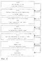
- FIG. 2 shows the block diagram of a process for the fabrication of a wire shaped solar cell described in the present invention. Said block diagram comprises the following steps:
- Figure 3 shows a schematic view of the incorporation step of nanoparticles in the outer conductor layer (405) applied in a preferred embodiment.
- a first step (301) the surface of the nanoparticles are functionalized by one or more chemical groups in the presence of a solvent characterized by high viscosity.
- Said solvent is selected from a group consisting of (1) a mix of Ethylene glycol (EG) and diethylene glycol monobutyl ether (DGME), (2) butyl acetate (BAc). Said solvent allows the nanoparticles to stay in suspension while functionalization is carried out.
- DGME diethylene glycol monobutyl ether
- BAc butyl acetate
- Said solvent allows the nanoparticles to stay in suspension while functionalization is carried out.
- the functionalized nanoparticles react with the host matrix through interaction with the chemical groups present on the nanoparticles surface.
- a thin film deposition is obtained over the active photovoltaic layer (403) using either dip coating or bar coating.
- a final curing method is required, dependent of the choice of the matrix.
- a temperature cure is used.
- an acrylate system the functional group present in the system permit a UV cure.
- a laser is used in order to fuse the nanoparticles into a film when no matrix is present.
- Figure 4 is an exemplary schematic diagram of an apparatus to perform a method according to any one or more of the compatible method embodiments described above, comprising:
- Figure 5 is an exemplary schematic diagram of an apparatus to perform a method according to any one or more of the compatible method embodiments described above, comprising:
- the wire core conductor is pre-treated in order to increase its performance in the final wire shaped coaxial solar cell.
- Said pre-treatment is preferably conducted at temperature not higher than 500°C, in the presence of an inert atmosphere or, alternatively, using a mixture of reactive gases.
- the metallic wires of the core conductor is selected from the group consisting of:
- a titanium dioxide layer is deposited on the core wire by dip coating or pultrusion coating to form a layer having a thickness between 50 and 500 nm, preferentially 150 nm.
- TiO2 diluted paste "Ti-Nanoxide T-L” from Solaronix is used to perform the coating. This paste allows a further curing at lower temperature compared to usual TiO2 formulations.
- a curing step is performed either by infrared or heat treatment. This curing step is required to evaporate the solvent from the TiO2 diluted paste. Heat or IR are set-up to provide a temperature comprised between 90 and 250°C to avoid oxidation on the core material.
- the 40 wt.% CH3NH3PbI3 precursor solution is prepared by reacting PbI2 (Aldrich, 98%) and as-prepared CH3NH3I powders with 1:1 molar ratio in the appropriate solvent.
- the HTM is deposited by dip coating or pultrusion coating at the speed of 1 to 3m/min.
- the HTM solution is prepared by dissolving copper thiocyanate (Sigma Aldrich) in propyl sulphide (Sigma Aldrich) at,6mg/mL.
- the active surface area of the PV fibre is 1.256 cm2 for 1m length. It corresponds to 1.75 mW/m of fibre and a current of 2.2 mA/m.
- Table 2 Electrical specifications of PV fibre/yarn Specification Value Test Method Priority Power generation Pout >1.5 mW/m (12W/m2) Under 1 sun irradiation, for 150um ⁇ diam. (active surface: 1 ⁇ 2 fibre surface) 1 Voltage Upmax > 600mV 1 Electrical current I pmax > 4 mA/m 1 Fill factor > 0.5 2
Landscapes
- Chemical & Material Sciences (AREA)
- Engineering & Computer Science (AREA)
- Materials Engineering (AREA)
- Physics & Mathematics (AREA)
- Electromagnetism (AREA)
- Inorganic Chemistry (AREA)
- Photovoltaic Devices (AREA)
Abstract
Description
- The invention relates to a coaxially wire shaped photovoltaic solid state solar cell (PSC) with an heterojunction comprising a perovskite material and a surface-increasing nanostructured semiconductor. The invention also relates to the method and the apparatus for the fabrication of said wire shaped PSC.
- Dye sensitized solar cells (DSCs) and solid state heterojunction solar cells show promising photovoltaic performance. Such devices have still to face several problems, which prevent them from achieving higher efficiencies, such as stability, low open circuit voltage and recombination issues. Said solar cells can't be efficiently be weaved and integrated in a textile to fabricate photovoltaic textiles.
- In addition it is very difficult to obtain efficient wire shaped solar cells capable to be weaved and integrated in a textile to fabricate photovoltaic textiles.
- Wire shaped photovoltaic cells are already known in the art, but known wire shaped solar cell technologies are based on DSCs technology which makes use of organometallic or organic dyes in conjunction with liquid or quasi-liquid electrolytes which dramatically lower long term stability and makes very difficult their manufacturing process.
- In recent years, wire-based DSCs have been reported for example in Fan et al. (Adv. Mater., 20, 592-595, 2008]. Wire-based DSCs have advantages such as lightweight and cost-effectiveness. However, the conversion efficiency (η) of these devices are lower compared with planar DSCs because the dye molecules are not allowed to absorb enough light through the electrolyte which has strong absorption at visible-light region.
- In the patent application
WO2014045021A1 is disclosed an optoelectronic devices having a thin film of a light- absorbing or light-emitting perovskite disposed between n-type (electron conducting) and p-type (hole conducting) layers. - In the,
patent application EP2693503A1 a solid-state solar cell with a solid state heterojunction is claimed, comprising a conducting support layer, on which a surface-increasing scaffold structure is provided, wherein an organic-inorganic perovskite layer is provided on said scaffold structure. - In said prior art documents no wire shaped solid state heterojunction solar cells has been described.
- The patent application
CN104009105A describes an invention based on the preparation of a linear electrode of transparent carbon nanometer tube plate perovskite CH3NH3PbI3 solar cell. This flexible braided coaxial linear perovskite solar cell comprises an electrode of stainless steel wire coated with a layer of nanotitanium dioxide particles, an active layer material of perovskite, a hole transport layer material and a final wrapping transparent carbon nanometer tube plate as another electrode. It is said that compared with the traditional planar structure of the solar battery, the claimed linear perovskite solar battery can be conveniently woven into fabric or other structure. - In the state of the art it is well known the disadvantages of wire or fiber shaped devices comprising liquid electrolytes, such as the problem of solvent evaporation and the penetration of water into the solar cell caused by difficulty in long-term stability and cell sealing especially in temperature cyclic tests.
- It is also well known the disadvantages of devices comprising expensive organic hole conductor materials, also known as hole transport materials (HTM), such as the incomplete pore filling which is observed with such hole conductors. Said hole conductor tends not to penetrate equally through the mesoporous film of sensitized solar cells using a porous semiconductor anode.
- Furthermore, in the state of the art it is still to be addressed the problem of oxidization of the hole conductor. Oxidation of the hole conductor may cause stability problems and lack of consistency.
- Furthermore, the present invention addresses the problem of low hole mobility observed with conductors used in the prior art, which are low compared to liquid electrolytes.
- The solar cell according to the present invention differs from previously known wire shaped solar cells because advantageously avoids the use of electrolytes.
- The invention provides an efficient wire shaped solar cell that can be prepared rapidly in an efficient way, using readily available, low-cost materials, using a short manufacturing procedure based on industrially known manufacturing steps.
- The present invention addresses the problems of stability observed with certain dye-sensitized solar cells.
- The present invention also addresses the advantage in manufacturing weavable photovoltaic devices by means of using photovoltaic fibers.
- The present invention provides a novel wire shaped coaxial solid state photovoltaic solar cell comprising several coaxial layers around, a core conducting wire. The present invention provides also methods for the fabrication of said wire shaped coaxial solid state photovoltaic solar cell by means of a coaxially deposition of several layers around a core conducting wire. The invention also relates to apparatus for the fabrication of said wire shaped solar cell.
- In an aspect, the present invention provides a solid-state solar cell comprising at least a conducting wire and a surface-increasing nanostructured semiconductor scaffold layer deposited on the outer surface of the wire, wherein one or more organic-inorganic perovskite layer is provided on said scaffold layer and wherein a counter electrode and/or metal layer is provided in electric contact with said perovskite layer without any hole transport material.
- In another aspect, the present invention provides a solid-state solar cell comprising at least a conducting wire and a surface-increasing nanostructured semiconductor scaffold layer deposited on the outer surface of the wire, wherein one or more organic-inorganic perovskite layer is provided on said scaffold layer and wherein a counter electrode and/or metal layer is provided in electric contact with said perovskite layer, said solid-state solar cell comprising a cheap hole transport material.
- The present invention addresses the advantage of avoiding the use of expensive organic HTM by means of an inorganic salt type hole conductor that is selected from the group of effective and cheap inorganic p-type hole-transporting material on perovskite-based devices. According to one embodiment said p-type hole-transporting material is an inorganic copper thiocyanate or an inorganic copper thiosulfate salt, diluted in a proper solvent.
- The coaxial solid state solar cell described in this invention has the following advantages over the dye-sensitized solar cells kwown in the state of the art:
- usable for realizing a photovoltaic fiber;
- a higher efficiency than a standard dye-sensitized solar cell;
- a higher flexibility and the need of less raw material;
- an easier fabrication and the absence of leakage, due to no use of liquid electrolyte;
- a wider solar spectrum available for conversion.
- In another aspect, the present invention provides a method for the fabrication of a coaxial solid state solar cell without any hole transport material, said method comprising at least the steps of:
- providing a conducting support layer on which a surface-increasing nanostructured semiconductor scaffold layer is deposited;
- applying one or more organic-inorganic perovskite layer on said scaffold structure; and,
- applying a counter electrode.
- In another aspect, the present invention provides a method of preparing a solid state solar cell, said method comprising at least the steps of:
- providing a conducting support layer on which a surface-increasing nanostructured semiconductor scaffold layer is deposited;
- applying one or more organic-inorganic perovskite layer on said scaffold structure;
- applying one copper thiocyanate layer on perovskite structure; and,
- applying a counter electrode.
- In another aspect the present invention includes an apparatus to perform a method according to any one or more of the compatible method embodiments described above, comprising: inner conductor unwinding servo feeder; different kind of curing means for the deposition processes and coating; winder servo tension control; control means, to control or regulate temperature and/or pressure and/or flowrate and/or other process parameters.
- In another aspect, the present invention provides an apparatus for the production of a wire shaped coaxial photovoltaic solar cell that comprising the following steps:
- pretreatment of conductive metallic wire shaped support with air temperature;
- treatment of the conductive metallic wire shaped support;
- deposition of a TiO2 nanostructured semiconductor scaffold layer and curing by IR radiation or heat treatment;
- deposition of one or more solid state perovskite layers;
- deposition of a counter electrode layer;
- deposition of a protective layer.
- In another aspect, the present invention provides an apparatus for the fabrication of a wire shaped coaxial photovoltaic solar cell that performs the following steps:
- pretreatment of conductive metallic wire shaped support with air temperature;
- treatment of the conductive metallic wire shaped support;
- deposition of a TiO2 nanostructured semiconductor scaffold layer and curing by IR radiation or heat treatment;
- deposition of one or more solid state perovskite layers;
- deposition of an inorganic hole transport layer
- deposition of a counter electrode layer;
- deposition of a protective layer.
- Further aspects and preferred embodiments of the invention are defined herein below and in the appended claims. Further features and advantages of the invention will become apparent to the skilled person from the description of the preferred embodiments given below.
-
-
Figure 1 provides a schematic circular section of the wire shaped photovoltaic solar cell according to one embodiment of the present invention. -
Figure 2 shows a block diagram of the process for the preparation of a wire shaped coaxial solar cell. -
Figure 3 shows a schematic view of the incorporation step of nanoparticles in the outer conductor layer of the wire shaped photovoltaic solar cell. -
Figure 4 shows a schematic view of a first apparatus for a continuous process for a wire shaped coaxial solar cell. -
Figure 5 shows a schematic view of a second apparatus for a continuous process for a wire shaped coaxial solar cell. -
Figures 1-5 are to be regarded as being purely exemplary and intended to illustrate the text, and not to limit the scope of the invention. - The present invention relates to a coaxially wire shaped photovoltaic solid state solar cell with an heterojunction comprising a perovskite material and a surface-increasing nanostructured semiconductor scaffold. The invention also relates to the methods for the fabrication of said solar cell and to the apparatus for the fabrication of said solar cell by means of applying said methods.
- According to an embodiment of the invention, the heterojunction comprises one or more layers of organic-inorganic perovskite, wherein said layers may each be the same or different.
- As used in the present invention the term "perovskite", refers to the "perovskite structure" and not specifically to the perovskite material, CaTiO3. For the purpose of this specification, "perovskite" describes any material that has the same type of crystal structure as calcium titanium oxide and of materials in which the bivalent cation is replaced by two separate monovalent cations. The perovskite structure has the general stoichiometry AMX3, where "A" and "M" are cations and "X" is an anion. The "A" and "M" cations can have a variety of charges and in the original Perovskite mineral (CaTiO3), the A cation is divalent and the M cation is tetravalent.
- For the purpose of this invention, the perovskite formulae includes structures having 3 or 4 anions, which may be the same or different, and/or one or two organic cations, and/or metal atoms carrying two or three positive charges.
- Typically organic-inorganic perovskites are hybrid materials exhibiting combined properties of organic composites and inorganic crystalline. The inorganic component forms a framework bound by covalent and ionic interactions which provide high carrier mobility. The organic component helps in the self-assembly process of these materials, it also enables the hybrid materials to be deposited by low-cost technique as other organic materials.
- In the present invention the perovskite is used in the form of one or more layers, said layers are organic-inorganic perovskite compounds of formula (I) :
[A,B]1,2[M,N][X]3,4 (I)
wherein: - A is a monovalent organic cation, in the form of A or A2;
- B is a bivalent organic cation;
- M is a metal atom;
- N is a metal atom;
- X is an anionic compound, in the form of X3 or X4.
- Preferably, A and B are selected from hydrocarbons comprising up to 15 carbons, and from 1 to 20 heteroatoms (for A) and 2 to 20 heteroatoms (for B), in particular one or two positively charged nitrogen atoms, respectively, besides possibly further heteroatoms selected from N, O and S. Furthermore, A and B may be partially or totally halogenated, independently of said 1 to 20 heteroatoms.
- M is a metal atom, which may be selected from the group consisting of Cu, Ni, Co, Fe2+, Mn2+, Cr2+, Pd2+, Cd2+, Ge2+, Sn2+, Pb2+, Eu2+, or Yb2+. Preferably, M is Sn2+ or Pb2+. N is a trivalent metal, which is preferably selected from the group of Bi3+ and Sb3+.
- X is an anionic compound, and is preferably selected independently from CI-, Br-, I-, NCS-, CN-, NCO-, and combinations thereof. As there may be three X in formulae (I), the perovskite material may comprise combinations of different halogens. For example, "X3" may be selected from I2Cl-3, I2Br-3, Cl2I-3, Br2I-3.
- The four anions in "X4" may also be a combination of different halogens. Preferably, X is Br- or I-.
- Not exhaustive examples of surface-increasing nanostructured semiconductor scaffold comprise Si, TiO2, SnO2, Fe2O3, ZnO, WO3, Nb2O5, CdS, ZnS, PbS, Bi2S3, CdSe, CdTe, SrTiO3, GaP, InP, GaAs, CuInS2, CuInSe2, and combinations thereof. Preferred semiconductor materials are Si, TiO2, SnO2, ZnO, WO3, Nb2O5 and SrTiO3.
- Not exhaustive examples of conducting wire shaped supports comprise Cu, Mo, Ti, Ni and W wires.
-
Figure 1 shows a transversal circular section of a preferred embodiment of the invention that preferentially comprises the following layers deposited coaxially around a core conductive wire: - a conductive wire shaped support and/or charge collector (401);
- a nanostructured semiconductor scaffold layer (402) ;
- a perovskite layer (403);
- an optional hole transporting materials layer (404);
- a counter electrode or outer conductor(405)
- an outer protective layer (406);
- Said wire shaped solar cell is a solid state dye solar cell, where a perovskite dye in the perovskite layer (403) is used instead of the standard electrolytic dye. The perovskite acts at the same time as a dye and as a dielectric.
- In a further preferred embodiment the wire shaped solar cell comprises the following layers deposited coaxially around a conductive wire:
- a conductive wire shaped support and/or charge collector (401);
- an additional primer layer (i);
- a nanostructured semiconductor scaffold layer (402);
- an additional protective layer (ii);
- one or more perovskite layers (403);
- an additional protective layer (iii);
- a counter electrode or outer conductor layer (405);
- an outer protective layer (406).
- In a further preferred embodiment the wire shaped solar cell comprises the following layers deposited coaxially around a conductive wire:
- a conductive wire shaped support and/or charge collector (401);
- an additional primer layer (i);
- a nanostructured semiconductor scaffold layer (402);
- an additional protective layer (ii);
- one or more perovskite layers (403);
- an inorganic hole conducting material layer (404);
- an additional protective layer (iii);
- a counter electrode or outer conductor layer (405);
- an outer protective layer (406).
- Said conductive wire shaped support and/or charge collector (401) is a metallic wire selected from the group consisting of Cu, Mo, Ti, Ni and W.
- Said inorganic hole conducting material layer (404) is preferentially consisting of copper thiocyanate.
- In a preferred embodiment said nanostructured semiconductor scaffold layer (402) is a titanium dioxide layer. Optimum efficiency is obtained with a TiO2 layer of 0.5um.
- Said counter electrode (405), also known as outer conductor, is a transparent conductive coating (TCC) applied directly on the top of the photovoltaic material. This enables a constant electrical conductivity on the fibre surface area.
- In a preferred embodiment of the invention nanoparticles are directly deposited on the active perovskite layer (403), wherein such deposition is preferentially made by means of a laser cure. Said nanoparticles are selected from the group consisting of Indium Tin Oxide (ITO), Antimony Tin Oxide (ATO), Cu nanoparticles, Ag nanoparticles.
- In another preferred embodiment said nanoparticles are preferentially incorporated in a matrix comprised in the outer conductor (405). Said matrix is a polymeric matrix selected from the group consisting of acrylate matrix and epoxy matrix. The epoxy matrix is characterized by low curing temperature. The acrylate matrix is characterized by UV curing condition. The nanoparticles incorporated in the matrix of the outer conductor (405) are selected from the group consisting of Indium Tin Oxide (ITO), Antimony Tin Oxide (ATO), Cu nanoparticles, Ag nanoparticles.
- In order to incorporate large quantity of nanoparticles in the outer conductor (405), such as up to 80% wt, the surface of said nanoparticles has to be modified (functionalization) by one or more chemical groups. Such one or more chemical groups react with the host matrix, if the host matrix is used. In a preferred embodiment said nanoparticles are functionalized using a reactant selected from the group consisting of epoxy silane, acrylate silane, mercapto silsesquioxane ligant (POSS).
- The outer protective layer (406) protects the electrically active layers of the wire shaped solar cell from shorting to any local electrical conductors and from any wear to adjacent surfaces. Said protective layer protects the overall photovoltaic layers from moisture and oxygen and give an electrical isolation. Furthermore this layer (406) gives to the invention the suitable properties for weaving (abrasion resistance, electrical resistance, high mechanical integrity, easy extrudability). In a preferred embodiment said protective layer (406) is highly transparent and is preferentially an acrylate based coating.
-
Figure 2 shows the block diagram of a process for the fabrication of a wire shaped solar cell described in the present invention. Said block diagram comprises the following steps: - (501) pre-treatment of the wire core conductor. Said core conductor is preferentially a metallic conductor selected from the group of metals consisting of: titanium, copper, molybdenum, tungsten, nickel. Specifications of said pretreatment are defined also taking into account the fiber performance and the requirements for interconnections, knitting and weaving properties.
- (502) cleaning the surface of the wire core conductor and/or depositing a primer layer, using at least one of the method selected from the group consisting of::
- a)UV-ozone cleaning;
- b)TiCl4 pre-treatment;
- c)sintering conducted at temperatures not higher than 500°C
- (503) deposition of a titanium dioxide layer on the wire core conductor, using at least one of the method selected from the group consisting of:
- ▪ a Chemical Bath Deposition (CBD) followed by an Atomic Layer Deposition (ALD);
- ▪ a TiO2 colloid dip coating followed by (ALD);
- ▪ a TiO2 diluted paste dip coating;
- ▪ a TiO2 diluted paste pultrusion coating;
- ▪ TiO2 Paste dip coating using wire pre-heat or TiCl4 primer as adhesion promoter;
- ▪ TiO2 growing from TiCl4 water based solution;
- ▪ TiO2 growing from TiCl4 sintering;
- ▪ Functionalization of TiO2 with Silane;
- ▪ Low temperature deposition;
- ▪ ALD deposition.
- (504) curing said titanium dioxide layer either by application of infrared radiation or by heat treatment.
- (505) deposition of a perovskite layer through wire dip coating or wire pultrusion coating using at least one of the method selected from the group consisting of:
- a) one step deposition process, preferably from a solution containing lead iodide, methylammonium iodide and dimethylformamide;
- b) two steps deposition process where the first step uses a solution containing lead iodide and dimethylformamide; and the second step uses a solution containing methylammonium iodide and Isopropanol. This is a faster deposition in order to not dissolve the previous lead iodide layer.
- (506) deposition of an optional inorganic CuSCN hole transport material layer.
- (507) deposition of the outer conductor layer (406) using a Transparent Conductive Oxide (TCO) alone or, alternatively, with a TCO followed by a second wire metallic core coated with platinum.
- (508) deposition of the outer protective coating using polymeric materials applied with dipping or pultruding technique and curing by heat or infrared, and UV.
-
Figure 3 shows a schematic view of the incorporation step of nanoparticles in the outer conductor layer (405) applied in a preferred embodiment. In a first step (301) the surface of the nanoparticles are functionalized by one or more chemical groups in the presence of a solvent characterized by high viscosity. Said solvent is selected from a group consisting of (1) a mix of Ethylene glycol (EG) and diethylene glycol monobutyl ether (DGME), (2) butyl acetate (BAc). Said solvent allows the nanoparticles to stay in suspension while functionalization is carried out. In a second step (302) the functionalized nanoparticles react with the host matrix through interaction with the chemical groups present on the nanoparticles surface. In a third step a thin film deposition is obtained over the active photovoltaic layer (403) using either dip coating or bar coating. A final curing method is required, dependent of the choice of the matrix. For an epoxy system, a temperature cure is used. For an acrylate system, the functional group present in the system permit a UV cure.
A laser is used in order to fuse the nanoparticles into a film when no matrix is present. -
Figure 4 is an exemplary schematic diagram of an apparatus to perform a method according to any one or more of the compatible method embodiments described above, comprising: - inner conductor unwinding servo feeder (601);
- conductive wire core material (615);
- means for performing cleaning step (602);
- means for performing deposition of electron transport layer and curing step (603);
- means for performing deposition of perovskite layer and curing step (604);
- means for performing deposition of the outer conductor layer and curing step (605);
- means for performing deposition of acrylate protective coating and curing step (606);
- means for performing UV curing (607);
- coaxially wire shaped photovoltaic solid state solar cell (608);
- winder servo tension control.
-
Figure 5 is an exemplary schematic diagram of an apparatus to perform a method according to any one or more of the compatible method embodiments described above, comprising: - inner conductor unwinding servo feeder (601);
- conductive wire core material (615);
- means for performing deposition of electron transport layer by means of pultrusion and following curing step (621);
- means for performing deposition of perovskite layer and curing step (622);
- means for performing deposition of inorganic hole transport material layer and curing step (623);
- means for performing deposition of the outer conductor layer and curing step (624);
- means for performing deposition of acrylate protective coating and curing step (625);
- means for performing UV curing (626);
- coaxially wire shaped photovoltaic solid state solar cell (627);
- winder servo tension control (640).
- For the scope of the present invention the above described apparatus, performing a method according to any one or more of the compatible method embodiments described above, takes advantage also by the use of
- a device to ensure the wire is centred to the nozzle when entering it so that the wire is coated evenly, and
- a device on which the nozzle size can be easily adapted to the diameter of the wire to that the deposited layer is even and smooth.
- In a preferred embodiment the wire core conductor is pre-treated in order to increase its performance in the final wire shaped coaxial solar cell. Said pre-treatment is preferably conducted at temperature not higher than 500°C, in the presence of an inert atmosphere or, alternatively, using a mixture of reactive gases.
- The metallic wires of the core conductor is selected from the group consisting of:
- 1. Titanium wire (Ti), with diameter comprised between 40 µm and 100 µm, preferentially 80µm;
- 2. Copper wire (Cu), with diameter comprised between 40 µm and 100 µm, preferentially 50 µm;
- 3. Molybdenum wire (Mo), with diameter comprised between 40 µm and 100 µm, preferentially 40 µm;
- 4. Tungsten wire (W), with diameter comprised between 40 µm and 100 µm, preferentially 70 µm;
- 5. Nickel wire (Ni), with diameter comprised between 40 µm and 100 µm, preferentially 80 µm.
- In a preferred embodiment a titanium dioxide layer is deposited on the core wire by dip coating or pultrusion coating to form a layer having a thickness between 50 and 500 nm, preferentially 150 nm.
- A commercially available TiO2 diluted paste "Ti-Nanoxide T-L" from Solaronix is used to perform the coating. This paste allows a further curing at lower temperature compared to usual TiO2 formulations.
- A curing step is performed either by infrared or heat treatment. This curing step is required to evaporate the solvent from the TiO2 diluted paste. Heat or IR are set-up to provide a temperature comprised between 90 and 250°C to avoid oxidation on the core material.
- In a preferred embodiment the 40 wt.% CH3NH3PbI3 precursor solution is prepared by reacting PbI2 (Aldrich, 98%) and as-prepared CH3NH3I powders with 1:1 molar ratio in the appropriate solvent.
- The HTM is deposited by dip coating or pultrusion coating at the speed of 1 to 3m/min. The HTM solution is prepared by dissolving copper thiocyanate (Sigma Aldrich) in propyl sulphide (Sigma Aldrich) at,6mg/mL.
- Some preferred realization of Perovskite devices based on synthesized semiconductors have been prepared and tested. Photovoltaic properties are summarized in a table below.
Table 1 ID ES/S+, V JSC, mA/cm2 VOC, mV FF η, % KR54 0.4 15.615 792 0.49 6.19 KR56 0.935 4.649 772 0.34 1.26 KR60 0.84 KR73 0.8 15.776 618 0.59 5.79 KR90 0.905 KR120 0.325 11.562 780 0.32 2.91 - Coating the protective layer (acrylates) by dip coating or pultrusion and curing the acrylate at 85°C to evaporate the solvent followed by UV curing (1 min at 2-3 J/cm2).
- In one preferred embodiment, the active surface area of the PV fibre is 1.256 cm2 for 1m length. It corresponds to 1.75 mW/m of fibre and a current of 2.2 mA/m.
Table 2: Electrical specifications of PV fibre/yarn Specification Value Test Method Priority Power generation Pout >1.5 mW/m (12W/m2) Under 1 sun irradiation, for 150um Ø diam. (active surface: ½ fibre surface) 1 Voltage Upmax > 600mV 1 Electrical current Ipmax > 4 mA/m 1 Fill factor > 0.5 2 - While the illustrative embodiments of the invention have been described with particularity, it will be understood that various other modifications will be apparent to and can be readily made by those skilled in the art without departing from the spirit and scope of the invention. Accordingly, it is not intended that the scope of the claims appended hereto be limited to the examples and descriptions set forth hereinabove but rather that the claims are construed as encompassing all the features of patentable novelty which reside in the present invention, including all features which would be treated as equivalents thereof by those skilled in the art to which the invention pertains.
Claims (15)
- "A wire shaped coaxial photovoltaic solar cell" comprising:- a conductive core wire shaped support (401),- a nanostructured semiconductor scaffold layer (402),- one or more successive perovskite layers (403),- an optionally provided hole transporting material layer (404),- an outer conductor layer (405),- an outer protective layer (406),characterized in that said outer conductor layer (405) comprises dispersed nanoparticles and said perovskite layers (403) are composed identically or wherein two or more of said layers have a different molecular structure and/or composition.
- The wire shaped coaxial photovoltaic solar cell according to claim 1 comprising:- an additional primer layer (i), positioned between the conductive core wire shaped support (401) and the nanostructured semiconductor scaffold layer (402),- an additional protective layer (ii), positioned between the nanostructured semiconductor scaffold layer (402) and the perovskite layers (403),- an additional protective layer (iii), positioned between the perovskite layers (403) and the outer conductor layer (405).
- The wire shaped coaxial photovoltaic solar cell according to any one of the preceding claims wherein the conductive core wire is a metallic wire selected from the group consisting of Cu, Mo, Ti, Ni, W, and wherein said wire has a diameter comprised between 40 µm and 100 µm.
- The wire shaped coaxial photovoltaic solar cell according to claim 1 wherein nanoparticles of the outer conductor layer (405) are dispersed in a polymeric matrix, preferably said matrix is acrylate matrix or epoxy matrix, said nanoparticles are selected from the group consisting o.f indium tin oxide, antimony tin oxide, copper nanoparticles, silver nanoparticles, and their related mixtures.
- The wire shaped coaxial photovoltaic solar cell according to claim 4 wherein said dispersed nanoparticles are functionalized with chemical groups selected from epoxy silane, acrylate silane, or their mixtures, said functionalization increasing dispersion and stability of nanoparticles in the polymeric matrix, permitting loading of nanoparticles up to 80% wt.
- The wire shaped coaxial photovoltaic solar cell according to claims 1, 2, 4 and 5 wherein the outer conductor (405) is a thin film of nanoparticles, said nanoparticles selected from the group consisting of indium tin oxide, antimony tin oxide, copper nanoparticles, silver nanoparticles, and their related mixtures.
- The wire shaped coaxial photovoltaic solar cell according to claim 6 wherein the nanoparticles of the thin film are nanoparticles functionalized with silsesquioxane ligand.
- The wire shaped coaxial photovoltaic solar cell according to any one of the preceding claims 1-7 where the outer protective layer (406) is a polymeric coating, preferably an acrylate based coating.
- The wire shaped coaxial photovoltaic solar cell according to any one of the preceding claims 1-8 where the nanostructured semiconductor scaffold layer (402) is a titanium dioxide nanostructured semiconductor scaffold layer.
- The wire shaped coaxial photovoltaic solar cell according to any one of the preceding claims 1-9 wherein the hole transporting material layer (404) is an inorganic copper thiocyanate or an inorganic copper thiosulfate salt, diluted in a solvent.
- A method for the fabrication of a wire shaped coaxial photovoltaic solar cell as in claim 1 and 2, the method comprises the following steps:- pretreatment of a conductive metallic wire shaped support (501),- cleaning the surface of the wire core conductor and/or depositing a primer layer (502),- deposition of a titanium dioxide layer on the wire core conductor (503),- curing said titanium dioxide layer either by application of infrared radiation or by heat treatment (505),- deposition of an optional inorganic hole transport material layer (506),- deposition of an outer conductor layer (507),- deposition of the outer protective coating (508).
- The method according to claim 11 wherein the cleaning step and/or depositing step (502) is preferentially performed using at least one of the method selected from the group consisting of:a)UV-ozone cleaning,b) TiCl4 pre-treatment,c)sintering conducted at temperatures not higher than 500°C.
- The method according to claim 11 wherein the deposition step (503) of a titanium dioxide layer is preferentially performed using at least one of the method selected from the group consisting of:- chemical bath deposition followed by an atomic layer deposition,- TiO2 colloid dip coating followed by atomic layer deposition,- TiO2 diluted paste dip coating,- TiO2 diluted paste pultrusion coating,- TiO2 paste dip coating using wire pre-heat or TiCl4 primer as adhesion promoter,- TiO2 growing from TiCl4 water based solution,- TiO2 growing from TiCl4 sintering,- functionalization of TiO2 with silane,- low temperature deposition,- atomic layer deposition.
- The method according to claim 11 wherein the deposition step (508) of the outer protective coating is preferentially performed using a polymeric materials applied with dipping or pultruding technique and curing by heat or infrared, and UV.
- An apparatus for the production of a wire shaped coaxial photovoltaic solar cell that performs the steps according to claim 11.
Priority Applications (2)
| Application Number | Priority Date | Filing Date | Title |
|---|---|---|---|
| EP15425096.3A EP3168877B1 (en) | 2015-11-13 | 2015-11-13 | A wire shaped coaxial photovoltaic solar cell |
| PCT/IB2016/001620 WO2017081531A1 (en) | 2015-11-13 | 2016-11-14 | A wire shaped coaxial photovoltaic solar cell |
Applications Claiming Priority (1)
| Application Number | Priority Date | Filing Date | Title |
|---|---|---|---|
| EP15425096.3A EP3168877B1 (en) | 2015-11-13 | 2015-11-13 | A wire shaped coaxial photovoltaic solar cell |
Publications (2)
| Publication Number | Publication Date |
|---|---|
| EP3168877A1 true EP3168877A1 (en) | 2017-05-17 |
| EP3168877B1 EP3168877B1 (en) | 2022-06-22 |
Family
ID=55070829
Family Applications (1)
| Application Number | Title | Priority Date | Filing Date |
|---|---|---|---|
| EP15425096.3A Not-in-force EP3168877B1 (en) | 2015-11-13 | 2015-11-13 | A wire shaped coaxial photovoltaic solar cell |
Country Status (2)
| Country | Link |
|---|---|
| EP (1) | EP3168877B1 (en) |
| WO (1) | WO2017081531A1 (en) |
Cited By (2)
| Publication number | Priority date | Publication date | Assignee | Title |
|---|---|---|---|---|
| KR20210078085A (en) * | 2019-12-18 | 2021-06-28 | 한국과학기술원 | Method for preparation of oxide support-nanoparticles composites |
| WO2022243970A1 (en) * | 2021-05-20 | 2022-11-24 | Universidade Do Porto | Coaxial energy harvesting and storage |
Families Citing this family (2)
| Publication number | Priority date | Publication date | Assignee | Title |
|---|---|---|---|---|
| CN113690372B (en) * | 2021-09-10 | 2024-05-28 | 华能新能源股份有限公司 | A perovskite solar cell and a method for preparing the same |
| CN114826146B (en) * | 2022-04-28 | 2023-07-25 | 哈尔滨工业大学 | Photo-thermal photovoltaic double-effect energy-saving glass |
Citations (4)
| Publication number | Priority date | Publication date | Assignee | Title |
|---|---|---|---|---|
| WO1993020569A1 (en) * | 1992-03-27 | 1993-10-14 | Sandoz Ltd. | Photovoltaic cells |
| EP2693503A1 (en) | 2012-08-03 | 2014-02-05 | Ecole Polytechnique Fédérale de Lausanne (EPFL) | Organo metal halide perovskite heterojunction solar cell and fabrication thereof |
| WO2014045021A1 (en) | 2012-09-18 | 2014-03-27 | Isis Innovation Limited | Optoelectronic device |
| CN104009105A (en) | 2014-06-11 | 2014-08-27 | 复旦大学 | A kind of linear perovskite solar cell and its preparation method |
Family Cites Families (1)
| Publication number | Priority date | Publication date | Assignee | Title |
|---|---|---|---|---|
| US9040816B2 (en) * | 2006-12-08 | 2015-05-26 | Nanocopoeia, Inc. | Methods and apparatus for forming photovoltaic cells using electrospray |
-
2015
- 2015-11-13 EP EP15425096.3A patent/EP3168877B1/en not_active Not-in-force
-
2016
- 2016-11-14 WO PCT/IB2016/001620 patent/WO2017081531A1/en not_active Ceased
Patent Citations (4)
| Publication number | Priority date | Publication date | Assignee | Title |
|---|---|---|---|---|
| WO1993020569A1 (en) * | 1992-03-27 | 1993-10-14 | Sandoz Ltd. | Photovoltaic cells |
| EP2693503A1 (en) | 2012-08-03 | 2014-02-05 | Ecole Polytechnique Fédérale de Lausanne (EPFL) | Organo metal halide perovskite heterojunction solar cell and fabrication thereof |
| WO2014045021A1 (en) | 2012-09-18 | 2014-03-27 | Isis Innovation Limited | Optoelectronic device |
| CN104009105A (en) | 2014-06-11 | 2014-08-27 | 复旦大学 | A kind of linear perovskite solar cell and its preparation method |
Non-Patent Citations (2)
| Title |
|---|
| FAN ET AL., ADV. MATER., vol. 20, 2008, pages 592 - 595 |
| LONGBIN QIU ET AL: "Integrating Perovskite Solar Cells into a Flexible Fiber", ANGEWANDTE CHEMIE INTERNATIONAL EDITION, vol. 53, no. 39, 22 September 2014 (2014-09-22), DE, pages 10425 - 10428, XP055271834, ISSN: 1433-7851, DOI: 10.1002/anie.201404973 * |
Cited By (2)
| Publication number | Priority date | Publication date | Assignee | Title |
|---|---|---|---|---|
| KR20210078085A (en) * | 2019-12-18 | 2021-06-28 | 한국과학기술원 | Method for preparation of oxide support-nanoparticles composites |
| WO2022243970A1 (en) * | 2021-05-20 | 2022-11-24 | Universidade Do Porto | Coaxial energy harvesting and storage |
Also Published As
| Publication number | Publication date |
|---|---|
| WO2017081531A1 (en) | 2017-05-18 |
| EP3168877B1 (en) | 2022-06-22 |
Similar Documents
| Publication | Publication Date | Title |
|---|---|---|
| AU2023204564B2 (en) | A Photovoltaic Device | |
| EP3017456B1 (en) | Solar cell and process for producing the same | |
| Mali et al. | Bio-inspired carbon hole transporting layer derived from aloe vera plant for cost-effective fully printable mesoscopic carbon perovskite solar cells | |
| EP2880698B1 (en) | Organo metal halide perovskite heterojunction solar cell and fabrication thereof | |
| Huangfu et al. | Copper iodide as inorganic hole conductor for perovskite solar cells with different thickness of mesoporous layer and hole transport layer | |
| KR20160004389A (en) | Organic-Inorganic Perovskite Based Solar Cell | |
| KR20190141742A (en) | Inorganic Hall Conductor Based Perovskite Photoelectric Conversion Device with Long-term High Operational Stability | |
| KR101635758B1 (en) | Sensitizing dye solution, working electrode prepared thereby, and dye-sensitized solar cell comprising the same | |
| Yang et al. | TiO 2 nanoparticle/nanofiber–ZnO photoanode for the enhancement of the efficiency of dye-sensitized solar cells | |
| EP3168877B1 (en) | A wire shaped coaxial photovoltaic solar cell | |
| KR20090065175A (en) | Dye-Sensitized Solar Cell and Manufacturing Method Thereof | |
| KR101694803B1 (en) | Perovskite solar cells comprising metal nanowire as photoelectrode, and the preparation method thereof | |
| KR101794988B1 (en) | Preparation method of perovskite absorber layer and preparation method of solarcell applied thereby | |
| KR102167415B1 (en) | Fabrication method of solar cells with metal chalcogenide-modified N-type semiconductors and solar cells prepared therefrom | |
| Zhu et al. | Preparation of ZnO electron transport layers by spray technology for perovskite solar cells | |
| KR101791801B1 (en) | Perovskite solar cells containing N-type semiconductors modified with chalcogens, and fabricating method therof | |
| Noola et al. | Cuprous thiocyanate as an inorganic hole transport material for carbon-based flexible perovskite solar cells | |
| KR101701670B1 (en) | Perovskite solar cells containing N-type semiconductors modified with oxygen and halogen atoms, and fabricating method thereof | |
| KR20250110912A (en) | Solar cells, solar modules and electrical devices | |
| JP2006278298A (en) | Method for producing dye-sensitized solar cell substrate and dye-sensitized solar cell substrate | |
| EP2538452A2 (en) | All-solid-state heterojunction solar cell | |
| Naidu et al. | Tuning recombination and charge separation in an/p/p heterojunction solar cell with CZTS, Ag 3 SbS 3 and a carbon interlayer | |
| Ameen et al. | Fabrication, doping and characterization of polyaniline and metal oxides: dye sensitized solar cells | |
| KR102966622B1 (en) | A method for preparing Transition-metal-incorporated MXene layers by electroplating, the MXene layers therefrom and hybrid solar cells with them | |
| KR102749667B1 (en) | Hybrid solar cells with transition-metal-incorporated MXene layer |
Legal Events
| Date | Code | Title | Description |
|---|---|---|---|
| PUAI | Public reference made under article 153(3) epc to a published international application that has entered the european phase |
Free format text: ORIGINAL CODE: 0009012 |
|
| STAA | Information on the status of an ep patent application or granted ep patent |
Free format text: STATUS: THE APPLICATION HAS BEEN PUBLISHED |
|
| AK | Designated contracting states |
Kind code of ref document: A1 Designated state(s): AL AT BE BG CH CY CZ DE DK EE ES FI FR GB GR HR HU IE IS IT LI LT LU LV MC MK MT NL NO PL PT RO RS SE SI SK SM TR |
|
| AX | Request for extension of the european patent |
Extension state: BA ME |
|
| STAA | Information on the status of an ep patent application or granted ep patent |
Free format text: STATUS: REQUEST FOR EXAMINATION WAS MADE |
|
| 17P | Request for examination filed |
Effective date: 20171116 |
|
| RBV | Designated contracting states (corrected) |
Designated state(s): AL AT BE BG CH CY CZ DE DK EE ES FI FR GB GR HR HU IE IS IT LI LT LU LV MC MK MT NL NO PL PT RO RS SE SI SK SM TR |
|
| RIC1 | Information provided on ipc code assigned before grant |
Ipc: H01L 51/42 20060101ALI20210209BHEP Ipc: H01L 27/30 20060101AFI20210209BHEP |
|
| GRAP | Despatch of communication of intention to grant a patent |
Free format text: ORIGINAL CODE: EPIDOSNIGR1 |
|
| STAA | Information on the status of an ep patent application or granted ep patent |
Free format text: STATUS: GRANT OF PATENT IS INTENDED |
|
| INTG | Intention to grant announced |
Effective date: 20210326 |
|
| GRAS | Grant fee paid |
Free format text: ORIGINAL CODE: EPIDOSNIGR3 |
|
| RAP3 | Party data changed (applicant data changed or rights of an application transferred) |
Owner name: CENTITVC CENTRE FOR NANOTECHNOLOGY AND SMART MATERIALS Owner name: BONAR N.V. Owner name: SCEYE INC |
|
| GRAA | (expected) grant |
Free format text: ORIGINAL CODE: 0009210 |
|
| STAA | Information on the status of an ep patent application or granted ep patent |
Free format text: STATUS: THE PATENT HAS BEEN GRANTED |
|
| AK | Designated contracting states |
Kind code of ref document: B1 Designated state(s): AL AT BE BG CH CY CZ DE DK EE ES FI FR GB GR HR HU IE IS IT LI LT LU LV MC MK MT NL NO PL PT RO RS SE SI SK SM TR |
|
| REG | Reference to a national code |
Ref country code: GB Ref legal event code: FG4D |
|
| REG | Reference to a national code |
Ref country code: CH Ref legal event code: EP |
|
| REG | Reference to a national code |
Ref country code: DE Ref legal event code: R096 Ref document number: 602015079531 Country of ref document: DE |
|
| REG | Reference to a national code |
Ref country code: AT Ref legal event code: REF Ref document number: 1500349 Country of ref document: AT Kind code of ref document: T Effective date: 20220715 |
|
| REG | Reference to a national code |
Ref country code: IE Ref legal event code: FG4D |
|
| REG | Reference to a national code |
Ref country code: LT Ref legal event code: MG9D |
|
| REG | Reference to a national code |
Ref country code: NL Ref legal event code: MP Effective date: 20220622 |
|
| PG25 | Lapsed in a contracting state [announced via postgrant information from national office to epo] |
Ref country code: SE Free format text: LAPSE BECAUSE OF FAILURE TO SUBMIT A TRANSLATION OF THE DESCRIPTION OR TO PAY THE FEE WITHIN THE PRESCRIBED TIME-LIMIT Effective date: 20220622 Ref country code: NO Free format text: LAPSE BECAUSE OF FAILURE TO SUBMIT A TRANSLATION OF THE DESCRIPTION OR TO PAY THE FEE WITHIN THE PRESCRIBED TIME-LIMIT Effective date: 20220922 Ref country code: LT Free format text: LAPSE BECAUSE OF FAILURE TO SUBMIT A TRANSLATION OF THE DESCRIPTION OR TO PAY THE FEE WITHIN THE PRESCRIBED TIME-LIMIT Effective date: 20220622 Ref country code: HR Free format text: LAPSE BECAUSE OF FAILURE TO SUBMIT A TRANSLATION OF THE DESCRIPTION OR TO PAY THE FEE WITHIN THE PRESCRIBED TIME-LIMIT Effective date: 20220622 Ref country code: FI Free format text: LAPSE BECAUSE OF FAILURE TO SUBMIT A TRANSLATION OF THE DESCRIPTION OR TO PAY THE FEE WITHIN THE PRESCRIBED TIME-LIMIT Effective date: 20220622 Ref country code: BG Free format text: LAPSE BECAUSE OF FAILURE TO SUBMIT A TRANSLATION OF THE DESCRIPTION OR TO PAY THE FEE WITHIN THE PRESCRIBED TIME-LIMIT Effective date: 20220922 |
|
| REG | Reference to a national code |
Ref country code: AT Ref legal event code: MK05 Ref document number: 1500349 Country of ref document: AT Kind code of ref document: T Effective date: 20220622 |
|
| REG | Reference to a national code |
Ref country code: DE Ref legal event code: R079 Ref document number: 602015079531 Country of ref document: DE Free format text: PREVIOUS MAIN CLASS: H01L0027300000 Ipc: H10K0039000000 |
|
| PG25 | Lapsed in a contracting state [announced via postgrant information from national office to epo] |
Ref country code: RS Free format text: LAPSE BECAUSE OF FAILURE TO SUBMIT A TRANSLATION OF THE DESCRIPTION OR TO PAY THE FEE WITHIN THE PRESCRIBED TIME-LIMIT Effective date: 20220622 Ref country code: LV Free format text: LAPSE BECAUSE OF FAILURE TO SUBMIT A TRANSLATION OF THE DESCRIPTION OR TO PAY THE FEE WITHIN THE PRESCRIBED TIME-LIMIT Effective date: 20220622 |
|
| PG25 | Lapsed in a contracting state [announced via postgrant information from national office to epo] |
Ref country code: NL Free format text: LAPSE BECAUSE OF FAILURE TO SUBMIT A TRANSLATION OF THE DESCRIPTION OR TO PAY THE FEE WITHIN THE PRESCRIBED TIME-LIMIT Effective date: 20220622 |
|
| PG25 | Lapsed in a contracting state [announced via postgrant information from national office to epo] |
Ref country code: SM Free format text: LAPSE BECAUSE OF FAILURE TO SUBMIT A TRANSLATION OF THE DESCRIPTION OR TO PAY THE FEE WITHIN THE PRESCRIBED TIME-LIMIT Effective date: 20220622 Ref country code: SK Free format text: LAPSE BECAUSE OF FAILURE TO SUBMIT A TRANSLATION OF THE DESCRIPTION OR TO PAY THE FEE WITHIN THE PRESCRIBED TIME-LIMIT Effective date: 20220622 Ref country code: RO Free format text: LAPSE BECAUSE OF FAILURE TO SUBMIT A TRANSLATION OF THE DESCRIPTION OR TO PAY THE FEE WITHIN THE PRESCRIBED TIME-LIMIT Effective date: 20220622 Ref country code: PT Free format text: LAPSE BECAUSE OF FAILURE TO SUBMIT A TRANSLATION OF THE DESCRIPTION OR TO PAY THE FEE WITHIN THE PRESCRIBED TIME-LIMIT Effective date: 20221024 Ref country code: ES Free format text: LAPSE BECAUSE OF FAILURE TO SUBMIT A TRANSLATION OF THE DESCRIPTION OR TO PAY THE FEE WITHIN THE PRESCRIBED TIME-LIMIT Effective date: 20220622 Ref country code: EE Free format text: LAPSE BECAUSE OF FAILURE TO SUBMIT A TRANSLATION OF THE DESCRIPTION OR TO PAY THE FEE WITHIN THE PRESCRIBED TIME-LIMIT Effective date: 20220622 Ref country code: CZ Free format text: LAPSE BECAUSE OF FAILURE TO SUBMIT A TRANSLATION OF THE DESCRIPTION OR TO PAY THE FEE WITHIN THE PRESCRIBED TIME-LIMIT Effective date: 20220622 Ref country code: AT Free format text: LAPSE BECAUSE OF FAILURE TO SUBMIT A TRANSLATION OF THE DESCRIPTION OR TO PAY THE FEE WITHIN THE PRESCRIBED TIME-LIMIT Effective date: 20220622 |
|
| PG25 | Lapsed in a contracting state [announced via postgrant information from national office to epo] |
Ref country code: PL Free format text: LAPSE BECAUSE OF FAILURE TO SUBMIT A TRANSLATION OF THE DESCRIPTION OR TO PAY THE FEE WITHIN THE PRESCRIBED TIME-LIMIT Effective date: 20220622 Ref country code: IS Free format text: LAPSE BECAUSE OF FAILURE TO SUBMIT A TRANSLATION OF THE DESCRIPTION OR TO PAY THE FEE WITHIN THE PRESCRIBED TIME-LIMIT Effective date: 20221022 |
|
| REG | Reference to a national code |
Ref country code: DE Ref legal event code: R097 Ref document number: 602015079531 Country of ref document: DE |
|
| PG25 | Lapsed in a contracting state [announced via postgrant information from national office to epo] |
Ref country code: AL Free format text: LAPSE BECAUSE OF FAILURE TO SUBMIT A TRANSLATION OF THE DESCRIPTION OR TO PAY THE FEE WITHIN THE PRESCRIBED TIME-LIMIT Effective date: 20220622 |
|
| PG25 | Lapsed in a contracting state [announced via postgrant information from national office to epo] |
Ref country code: DK Free format text: LAPSE BECAUSE OF FAILURE TO SUBMIT A TRANSLATION OF THE DESCRIPTION OR TO PAY THE FEE WITHIN THE PRESCRIBED TIME-LIMIT Effective date: 20220622 |
|
| PLBE | No opposition filed within time limit |
Free format text: ORIGINAL CODE: 0009261 |
|
| STAA | Information on the status of an ep patent application or granted ep patent |
Free format text: STATUS: NO OPPOSITION FILED WITHIN TIME LIMIT |
|
| 26N | No opposition filed |
Effective date: 20230323 |
|
| REG | Reference to a national code |
Ref country code: DE Ref legal event code: R119 Ref document number: 602015079531 Country of ref document: DE |
|
| PG25 | Lapsed in a contracting state [announced via postgrant information from national office to epo] |
Ref country code: MC Free format text: LAPSE BECAUSE OF FAILURE TO SUBMIT A TRANSLATION OF THE DESCRIPTION OR TO PAY THE FEE WITHIN THE PRESCRIBED TIME-LIMIT Effective date: 20220622 |
|
| REG | Reference to a national code |
Ref country code: CH Ref legal event code: PL |
|
| GBPC | Gb: european patent ceased through non-payment of renewal fee |
Effective date: 20221113 |
|
| REG | Reference to a national code |
Ref country code: BE Ref legal event code: MM Effective date: 20221130 |
|
| PG25 | Lapsed in a contracting state [announced via postgrant information from national office to epo] |
Ref country code: LI Free format text: LAPSE BECAUSE OF NON-PAYMENT OF DUE FEES Effective date: 20221130 Ref country code: CH Free format text: LAPSE BECAUSE OF NON-PAYMENT OF DUE FEES Effective date: 20221130 |
|
| PG25 | Lapsed in a contracting state [announced via postgrant information from national office to epo] |
Ref country code: SI Free format text: LAPSE BECAUSE OF FAILURE TO SUBMIT A TRANSLATION OF THE DESCRIPTION OR TO PAY THE FEE WITHIN THE PRESCRIBED TIME-LIMIT Effective date: 20220622 Ref country code: LU Free format text: LAPSE BECAUSE OF NON-PAYMENT OF DUE FEES Effective date: 20221113 |
|
| PG25 | Lapsed in a contracting state [announced via postgrant information from national office to epo] |
Ref country code: IE Free format text: LAPSE BECAUSE OF NON-PAYMENT OF DUE FEES Effective date: 20221113 Ref country code: GB Free format text: LAPSE BECAUSE OF NON-PAYMENT OF DUE FEES Effective date: 20221113 Ref country code: DE Free format text: LAPSE BECAUSE OF NON-PAYMENT OF DUE FEES Effective date: 20230601 |
|
| PG25 | Lapsed in a contracting state [announced via postgrant information from national office to epo] |
Ref country code: FR Free format text: LAPSE BECAUSE OF NON-PAYMENT OF DUE FEES Effective date: 20221130 Ref country code: BE Free format text: LAPSE BECAUSE OF NON-PAYMENT OF DUE FEES Effective date: 20221130 |
|
| PG25 | Lapsed in a contracting state [announced via postgrant information from national office to epo] |
Ref country code: IT Free format text: LAPSE BECAUSE OF FAILURE TO SUBMIT A TRANSLATION OF THE DESCRIPTION OR TO PAY THE FEE WITHIN THE PRESCRIBED TIME-LIMIT Effective date: 20220622 |
|
| PG25 | Lapsed in a contracting state [announced via postgrant information from national office to epo] |
Ref country code: HU Free format text: LAPSE BECAUSE OF FAILURE TO SUBMIT A TRANSLATION OF THE DESCRIPTION OR TO PAY THE FEE WITHIN THE PRESCRIBED TIME-LIMIT; INVALID AB INITIO Effective date: 20151113 |
|
| PG25 | Lapsed in a contracting state [announced via postgrant information from national office to epo] |
Ref country code: CY Free format text: LAPSE BECAUSE OF FAILURE TO SUBMIT A TRANSLATION OF THE DESCRIPTION OR TO PAY THE FEE WITHIN THE PRESCRIBED TIME-LIMIT Effective date: 20220622 |
|
| PG25 | Lapsed in a contracting state [announced via postgrant information from national office to epo] |
Ref country code: MK Free format text: LAPSE BECAUSE OF FAILURE TO SUBMIT A TRANSLATION OF THE DESCRIPTION OR TO PAY THE FEE WITHIN THE PRESCRIBED TIME-LIMIT Effective date: 20220622 |
|
| PG25 | Lapsed in a contracting state [announced via postgrant information from national office to epo] |
Ref country code: MT Free format text: LAPSE BECAUSE OF FAILURE TO SUBMIT A TRANSLATION OF THE DESCRIPTION OR TO PAY THE FEE WITHIN THE PRESCRIBED TIME-LIMIT Effective date: 20220622 |
|
| PG25 | Lapsed in a contracting state [announced via postgrant information from national office to epo] |
Ref country code: BG Free format text: LAPSE BECAUSE OF FAILURE TO SUBMIT A TRANSLATION OF THE DESCRIPTION OR TO PAY THE FEE WITHIN THE PRESCRIBED TIME-LIMIT Effective date: 20220622 |
|
| PG25 | Lapsed in a contracting state [announced via postgrant information from national office to epo] |
Ref country code: BG Free format text: LAPSE BECAUSE OF FAILURE TO SUBMIT A TRANSLATION OF THE DESCRIPTION OR TO PAY THE FEE WITHIN THE PRESCRIBED TIME-LIMIT Effective date: 20220622 |
|
| PG25 | Lapsed in a contracting state [announced via postgrant information from national office to epo] |
Ref country code: GR Free format text: LAPSE BECAUSE OF NON-PAYMENT OF DUE FEES Effective date: 20220622 |
|
| PG25 | Lapsed in a contracting state [announced via postgrant information from national office to epo] |
Ref country code: GR Free format text: LAPSE BECAUSE OF NON-PAYMENT OF DUE FEES Effective date: 20220622 |
|
| PG25 | Lapsed in a contracting state [announced via postgrant information from national office to epo] |
Ref country code: TR Free format text: LAPSE BECAUSE OF FAILURE TO SUBMIT A TRANSLATION OF THE DESCRIPTION OR TO PAY THE FEE WITHIN THE PRESCRIBED TIME-LIMIT Effective date: 20220622 |