EP3168331A1 - Nanostrukturiertes material, herstellungsverfahren und verwendung davon - Google Patents
Nanostrukturiertes material, herstellungsverfahren und verwendung davon Download PDFInfo
- Publication number
- EP3168331A1 EP3168331A1 EP15818949.8A EP15818949A EP3168331A1 EP 3168331 A1 EP3168331 A1 EP 3168331A1 EP 15818949 A EP15818949 A EP 15818949A EP 3168331 A1 EP3168331 A1 EP 3168331A1
- Authority
- EP
- European Patent Office
- Prior art keywords
- pores
- longitudinal
- anodizing
- pore
- nanostructured material
- Prior art date
- Legal status (The legal status is an assumption and is not a legal conclusion. Google has not performed a legal analysis and makes no representation as to the accuracy of the status listed.)
- Withdrawn
Links
Images


Classifications
-
- H—ELECTRICITY
- H01—ELECTRIC ELEMENTS
- H01B—CABLES; CONDUCTORS; INSULATORS; SELECTION OF MATERIALS FOR THEIR CONDUCTIVE, INSULATING OR DIELECTRIC PROPERTIES
- H01B1/00—Conductors or conductive bodies characterised by the conductive materials; Selection of materials as conductors
- H01B1/02—Conductors or conductive bodies characterised by the conductive materials; Selection of materials as conductors mainly consisting of metals or alloys
- H01B1/023—Alloys based on aluminium
-
- B—PERFORMING OPERATIONS; TRANSPORTING
- B29—WORKING OF PLASTICS; WORKING OF SUBSTANCES IN A PLASTIC STATE IN GENERAL
- B29C—SHAPING OR JOINING OF PLASTICS; SHAPING OF MATERIAL IN A PLASTIC STATE, NOT OTHERWISE PROVIDED FOR; AFTER-TREATMENT OF THE SHAPED PRODUCTS, e.g. REPAIRING
- B29C39/00—Shaping by casting, i.e. introducing the moulding material into a mould or between confining surfaces without significant moulding pressure; Apparatus therefor
- B29C39/02—Shaping by casting, i.e. introducing the moulding material into a mould or between confining surfaces without significant moulding pressure; Apparatus therefor for making articles of definite length, i.e. discrete articles
- B29C39/026—Shaping by casting, i.e. introducing the moulding material into a mould or between confining surfaces without significant moulding pressure; Apparatus therefor for making articles of definite length, i.e. discrete articles characterised by the shape of the surface
-
- B—PERFORMING OPERATIONS; TRANSPORTING
- B29—WORKING OF PLASTICS; WORKING OF SUBSTANCES IN A PLASTIC STATE IN GENERAL
- B29C—SHAPING OR JOINING OF PLASTICS; SHAPING OF MATERIAL IN A PLASTIC STATE, NOT OTHERWISE PROVIDED FOR; AFTER-TREATMENT OF THE SHAPED PRODUCTS, e.g. REPAIRING
- B29C39/00—Shaping by casting, i.e. introducing the moulding material into a mould or between confining surfaces without significant moulding pressure; Apparatus therefor
- B29C39/22—Component parts, details or accessories; Auxiliary operations
- B29C39/36—Removing moulded articles
-
- B—PERFORMING OPERATIONS; TRANSPORTING
- B82—NANOTECHNOLOGY
- B82Y—SPECIFIC USES OR APPLICATIONS OF NANOSTRUCTURES; MEASUREMENT OR ANALYSIS OF NANOSTRUCTURES; MANUFACTURE OR TREATMENT OF NANOSTRUCTURES
- B82Y30/00—Nanotechnology for materials or surface science, e.g. nanocomposites
-
- B—PERFORMING OPERATIONS; TRANSPORTING
- B82—NANOTECHNOLOGY
- B82Y—SPECIFIC USES OR APPLICATIONS OF NANOSTRUCTURES; MEASUREMENT OR ANALYSIS OF NANOSTRUCTURES; MANUFACTURE OR TREATMENT OF NANOSTRUCTURES
- B82Y40/00—Manufacture or treatment of nanostructures
-
- C—CHEMISTRY; METALLURGY
- C01—INORGANIC CHEMISTRY
- C01F—COMPOUNDS OF THE METALS BERYLLIUM, MAGNESIUM, ALUMINIUM, CALCIUM, STRONTIUM, BARIUM, RADIUM, THORIUM, OR OF THE RARE-EARTH METALS
- C01F7/00—Compounds of aluminium
- C01F7/02—Aluminium oxide; Aluminium hydroxide; Aluminates
-
- C—CHEMISTRY; METALLURGY
- C08—ORGANIC MACROMOLECULAR COMPOUNDS; THEIR PREPARATION OR CHEMICAL WORKING-UP; COMPOSITIONS BASED THEREON
- C08J—WORKING-UP; GENERAL PROCESSES OF COMPOUNDING; AFTER-TREATMENT NOT COVERED BY SUBCLASSES C08B, C08C, C08F, C08G or C08H
- C08J9/00—Working-up of macromolecular substances to porous or cellular articles or materials; After-treatment thereof
- C08J9/26—Working-up of macromolecular substances to porous or cellular articles or materials; After-treatment thereof by elimination of a solid phase from a macromolecular composition or article, e.g. leaching out
-
- C—CHEMISTRY; METALLURGY
- C25—ELECTROLYTIC OR ELECTROPHORETIC PROCESSES; APPARATUS THEREFOR
- C25D—PROCESSES FOR THE ELECTROLYTIC OR ELECTROPHORETIC PRODUCTION OF COATINGS; ELECTROFORMING; APPARATUS THEREFOR
- C25D11/00—Electrolytic coating by surface reaction, i.e. forming conversion layers
- C25D11/02—Anodisation
- C25D11/024—Anodisation under pulsed or modulated current or potential
-
- C—CHEMISTRY; METALLURGY
- C25—ELECTROLYTIC OR ELECTROPHORETIC PROCESSES; APPARATUS THEREFOR
- C25D—PROCESSES FOR THE ELECTROLYTIC OR ELECTROPHORETIC PRODUCTION OF COATINGS; ELECTROFORMING; APPARATUS THEREFOR
- C25D11/00—Electrolytic coating by surface reaction, i.e. forming conversion layers
- C25D11/02—Anodisation
- C25D11/026—Anodisation with spark discharge
-
- C—CHEMISTRY; METALLURGY
- C25—ELECTROLYTIC OR ELECTROPHORETIC PROCESSES; APPARATUS THEREFOR
- C25D—PROCESSES FOR THE ELECTROLYTIC OR ELECTROPHORETIC PRODUCTION OF COATINGS; ELECTROFORMING; APPARATUS THEREFOR
- C25D11/00—Electrolytic coating by surface reaction, i.e. forming conversion layers
- C25D11/02—Anodisation
- C25D11/04—Anodisation of aluminium or alloys based thereon
- C25D11/045—Anodisation of aluminium or alloys based thereon for forming AAO templates
-
- C—CHEMISTRY; METALLURGY
- C25—ELECTROLYTIC OR ELECTROPHORETIC PROCESSES; APPARATUS THEREFOR
- C25D—PROCESSES FOR THE ELECTROLYTIC OR ELECTROPHORETIC PRODUCTION OF COATINGS; ELECTROFORMING; APPARATUS THEREFOR
- C25D11/00—Electrolytic coating by surface reaction, i.e. forming conversion layers
- C25D11/02—Anodisation
- C25D11/04—Anodisation of aluminium or alloys based thereon
- C25D11/06—Anodisation of aluminium or alloys based thereon characterised by the electrolytes used
- C25D11/08—Anodisation of aluminium or alloys based thereon characterised by the electrolytes used containing inorganic acids
-
- C—CHEMISTRY; METALLURGY
- C25—ELECTROLYTIC OR ELECTROPHORETIC PROCESSES; APPARATUS THEREFOR
- C25D—PROCESSES FOR THE ELECTROLYTIC OR ELECTROPHORETIC PRODUCTION OF COATINGS; ELECTROFORMING; APPARATUS THEREFOR
- C25D11/00—Electrolytic coating by surface reaction, i.e. forming conversion layers
- C25D11/02—Anodisation
- C25D11/04—Anodisation of aluminium or alloys based thereon
- C25D11/12—Anodising more than once, e.g. in different baths
-
- C—CHEMISTRY; METALLURGY
- C25—ELECTROLYTIC OR ELECTROPHORETIC PROCESSES; APPARATUS THEREFOR
- C25D—PROCESSES FOR THE ELECTROLYTIC OR ELECTROPHORETIC PRODUCTION OF COATINGS; ELECTROFORMING; APPARATUS THEREFOR
- C25D11/00—Electrolytic coating by surface reaction, i.e. forming conversion layers
- C25D11/02—Anodisation
- C25D11/04—Anodisation of aluminium or alloys based thereon
- C25D11/16—Pretreatment, e.g. desmutting
-
- C—CHEMISTRY; METALLURGY
- C25—ELECTROLYTIC OR ELECTROPHORETIC PROCESSES; APPARATUS THEREFOR
- C25D—PROCESSES FOR THE ELECTROLYTIC OR ELECTROPHORETIC PRODUCTION OF COATINGS; ELECTROFORMING; APPARATUS THEREFOR
- C25D11/00—Electrolytic coating by surface reaction, i.e. forming conversion layers
- C25D11/02—Anodisation
- C25D11/04—Anodisation of aluminium or alloys based thereon
- C25D11/18—After-treatment, e.g. pore-sealing
- C25D11/24—Chemical after-treatment
-
- C—CHEMISTRY; METALLURGY
- C25—ELECTROLYTIC OR ELECTROPHORETIC PROCESSES; APPARATUS THEREFOR
- C25F—PROCESSES FOR THE ELECTROLYTIC REMOVAL OF MATERIALS FROM OBJECTS; APPARATUS THEREFOR
- C25F3/00—Electrolytic etching or polishing
- C25F3/16—Polishing
- C25F3/18—Polishing of light metals
- C25F3/20—Polishing of light metals of aluminium
-
- B—PERFORMING OPERATIONS; TRANSPORTING
- B29—WORKING OF PLASTICS; WORKING OF SUBSTANCES IN A PLASTIC STATE IN GENERAL
- B29K—INDEXING SCHEME ASSOCIATED WITH SUBCLASSES B29B, B29C OR B29D, RELATING TO MOULDING MATERIALS OR TO MATERIALS FOR MOULDS, REINFORCEMENTS, FILLERS OR PREFORMED PARTS, e.g. INSERTS
- B29K2025/00—Use of polymers of vinyl-aromatic compounds or derivatives thereof as moulding material
- B29K2025/04—Polymers of styrene
- B29K2025/06—PS, i.e. polystyrene
-
- C—CHEMISTRY; METALLURGY
- C01—INORGANIC CHEMISTRY
- C01P—INDEXING SCHEME RELATING TO STRUCTURAL AND PHYSICAL ASPECTS OF SOLID INORGANIC COMPOUNDS
- C01P2006/00—Physical properties of inorganic compounds
- C01P2006/16—Pore diameter
-
- C—CHEMISTRY; METALLURGY
- C08—ORGANIC MACROMOLECULAR COMPOUNDS; THEIR PREPARATION OR CHEMICAL WORKING-UP; COMPOSITIONS BASED THEREON
- C08J—WORKING-UP; GENERAL PROCESSES OF COMPOUNDING; AFTER-TREATMENT NOT COVERED BY SUBCLASSES C08B, C08C, C08F, C08G or C08H
- C08J2201/00—Foams characterised by the foaming process
- C08J2201/02—Foams characterised by the foaming process characterised by mechanical pre- or post-treatments
- C08J2201/038—Use of an inorganic compound to impregnate, bind or coat a foam, e.g. waterglass
-
- C—CHEMISTRY; METALLURGY
- C08—ORGANIC MACROMOLECULAR COMPOUNDS; THEIR PREPARATION OR CHEMICAL WORKING-UP; COMPOSITIONS BASED THEREON
- C08J—WORKING-UP; GENERAL PROCESSES OF COMPOUNDING; AFTER-TREATMENT NOT COVERED BY SUBCLASSES C08B, C08C, C08F, C08G or C08H
- C08J2201/00—Foams characterised by the foaming process
- C08J2201/04—Foams characterised by the foaming process characterised by the elimination of a liquid or solid component, e.g. precipitation, leaching out, evaporation
- C08J2201/044—Elimination of an inorganic solid phase
- C08J2201/0442—Elimination of an inorganic solid phase the inorganic phase being a metal, its oxide or hydroxide
-
- C—CHEMISTRY; METALLURGY
- C08—ORGANIC MACROMOLECULAR COMPOUNDS; THEIR PREPARATION OR CHEMICAL WORKING-UP; COMPOSITIONS BASED THEREON
- C08J—WORKING-UP; GENERAL PROCESSES OF COMPOUNDING; AFTER-TREATMENT NOT COVERED BY SUBCLASSES C08B, C08C, C08F, C08G or C08H
- C08J2325/00—Characterised by the use of homopolymers or copolymers of compounds having one or more unsaturated aliphatic radicals, each having only one carbon-to-carbon double bond, and at least one being terminated by an aromatic carbocyclic ring; Derivatives of such polymers
- C08J2325/02—Homopolymers or copolymers of hydrocarbons
- C08J2325/04—Homopolymers or copolymers of styrene
- C08J2325/06—Polystyrene
-
- Y—GENERAL TAGGING OF NEW TECHNOLOGICAL DEVELOPMENTS; GENERAL TAGGING OF CROSS-SECTIONAL TECHNOLOGIES SPANNING OVER SEVERAL SECTIONS OF THE IPC; TECHNICAL SUBJECTS COVERED BY FORMER USPC CROSS-REFERENCE ART COLLECTIONS [XRACs] AND DIGESTS
- Y10—TECHNICAL SUBJECTS COVERED BY FORMER USPC
- Y10S—TECHNICAL SUBJECTS COVERED BY FORMER USPC CROSS-REFERENCE ART COLLECTIONS [XRACs] AND DIGESTS
- Y10S977/00—Nanotechnology
- Y10S977/70—Nanostructure
- Y10S977/762—Nanowire or quantum wire, i.e. axially elongated structure having two dimensions of 100 nm or less
-
- Y—GENERAL TAGGING OF NEW TECHNOLOGICAL DEVELOPMENTS; GENERAL TAGGING OF CROSS-SECTIONAL TECHNOLOGIES SPANNING OVER SEVERAL SECTIONS OF THE IPC; TECHNICAL SUBJECTS COVERED BY FORMER USPC CROSS-REFERENCE ART COLLECTIONS [XRACs] AND DIGESTS
- Y10—TECHNICAL SUBJECTS COVERED BY FORMER USPC
- Y10S—TECHNICAL SUBJECTS COVERED BY FORMER USPC CROSS-REFERENCE ART COLLECTIONS [XRACs] AND DIGESTS
- Y10S977/00—Nanotechnology
- Y10S977/70—Nanostructure
- Y10S977/788—Of specified organic or carbon-based composition
-
- Y—GENERAL TAGGING OF NEW TECHNOLOGICAL DEVELOPMENTS; GENERAL TAGGING OF CROSS-SECTIONAL TECHNOLOGIES SPANNING OVER SEVERAL SECTIONS OF THE IPC; TECHNICAL SUBJECTS COVERED BY FORMER USPC CROSS-REFERENCE ART COLLECTIONS [XRACs] AND DIGESTS
- Y10—TECHNICAL SUBJECTS COVERED BY FORMER USPC
- Y10S—TECHNICAL SUBJECTS COVERED BY FORMER USPC CROSS-REFERENCE ART COLLECTIONS [XRACs] AND DIGESTS
- Y10S977/00—Nanotechnology
- Y10S977/84—Manufacture, treatment, or detection of nanostructure
- Y10S977/89—Deposition of materials, e.g. coating, cvd, or ald
- Y10S977/893—Deposition in pores, molding, with subsequent removal of mold
-
- Y—GENERAL TAGGING OF NEW TECHNOLOGICAL DEVELOPMENTS; GENERAL TAGGING OF CROSS-SECTIONAL TECHNOLOGIES SPANNING OVER SEVERAL SECTIONS OF THE IPC; TECHNICAL SUBJECTS COVERED BY FORMER USPC CROSS-REFERENCE ART COLLECTIONS [XRACs] AND DIGESTS
- Y10—TECHNICAL SUBJECTS COVERED BY FORMER USPC
- Y10S—TECHNICAL SUBJECTS COVERED BY FORMER USPC CROSS-REFERENCE ART COLLECTIONS [XRACs] AND DIGESTS
- Y10S977/00—Nanotechnology
- Y10S977/84—Manufacture, treatment, or detection of nanostructure
- Y10S977/895—Manufacture, treatment, or detection of nanostructure having step or means utilizing chemical property
- Y10S977/896—Chemical synthesis, e.g. chemical bonding or breaking
- Y10S977/897—Polymerization
Definitions
- the object of the invention is a nanostructured anodized aluminium material, in addition to its corresponding manufacturing process and eventual uses of the nanostructured anodized aluminium material, which is particularly suitable as a mould for the production of nanostructures.
- the material object of the invention is constituted by a homogeneous hexagonal lattice of parallel cylindrical nanotubes arranged perpendicularly to the anodized surface and which are interconnected by pores located in planes parallel to the anodized surface.
- Anodizing is an electrolytic passivation process used to increase the thickness of the natural oxide layer on the surface of metal parts. This technique is often used on aluminium to generate an artificial protective oxide layer, known as anodic aluminium oxide (AAO).
- AAO anodic aluminium oxide
- the layer is achieved using electrochemical processes and provides an electrically insulating surface with greater chemical and mechanical resistance that increases the durability of the aluminum. The process owes its name to the fact that the part to be treated with this material acts as an anode in the electrical circuit during the electrolytic process.
- Anodizing is used to protect metals such as aluminium and titanium from abrasion and corrosion, providing, besides protection, aesthetic advantages by dyeing the surface.
- Anodizing techniques have evolved considerably over time, ranging from a layer of aluminium oxide in its natural white colour to dyeing subsequent to the formation of the layer with colours such as gold, bronze, black and red.
- pores parallel therebetween and perpendicular to the surface of the initial substrate are generated. These pores are called longitudinal pores and are characterised in that they constitute a hexagonal lattice.
- the longitudinal pores have diameters of less than 0.5 pm, pores of submicron diameter, even reaching nanometric diameters below 100 nm.
- Pore diameter is controlled by the type of electrolyte used in the anodizing process. Pore diameter is controlled through the type of electrolyte used in the anodizing process. Microscopic pore modification is achieved by reproducing the temperature conditions, electrolyte concentrations, voltages, agitation control, affected load surface and alloy characteristics.
- the growth processes of the anodized alumina film at lower anodizing potentials are slow and require several days of processing for a thickness of a few tens of micrometres.
- hard anodizing makes it possible to increase rate of growth, thereby achieving greater thicknesses.
- higher electric current densities than in mild anodizing are generally used, making it possible to modify the diameter of the longitudinal nanostructures, producing pores with larger diameters.
- EP1884578A1 discloses an anodizing process based on oxalic acid for ordered alumina membranes, which can be easily implemented in nanotechnology and in industry.
- the process is an improvement of so-called "hard anodizing" which has been widely used since the 1960s in the industry for high-speed manufacturing of elements having good mechanical characteristics, high thickness (>100 pm) and low anodic alumina film porosity.
- the anodized alumina films can serve as well-defined two-dimenionsional (2D) nanoarchitectures that can be applied in different nanotechnologies, such as photonic crystals, metamaterials, micromembranes, filters or moulds for synthesis in the manufacture of nanostructures such as nanowire and nanotube materials of very diverse nature.
- 2D two-dimenionsional
- anodic alumina have been used as patterns or nano-moulds for manufacturing nanostructures, particularly nanowires and nanotubes, as shown, for example, by Masuda, H. and K. Fukuda (Science, 1995. 268 (5216): p. 1466-1468 ).
- the pores of the anodized alumina film are filled by means of various methods consisting of electrodeposition processes, atomic layer deposition, melt-infiltration, sol-gel, in situ polymerisation or crystallisation, vapor phase deposition, etc.
- nanostructured materials obtained by means of the aforementioned methods are metal nanowires, semiconductor nanowires, or polymers formed in the interior of the longitudinal pores of the anodized alumina film.
- nanowires or nanotubes perpendicular to the substrate surface is obtained.
- the nanowires or nanotubes can be extracted from the matrix by selective dissolution of the alumina film in acidic and basic media.
- scattered and separated nanowires or nanotubes are obtained.
- materials currently exist having an ordered (periodic) and three-dimensional porous structure in the range of sizes of the porous structure of the AAO they are systems produced from continuous block copolymer (BC) phases of the gyroid type, double gyroid type, etc.
- BC block copolymer
- the use of AAO materials as nano-moulds has some advantages over the use of BC materials for the manufacture of ordered nanostructures:
- a limitation of the state of the art in the dying of anodized alumina layers consists of the fact that the pigment colours appear the same from all viewing angles, since the films do not exhibit structural-type colours as a result of selective reflection or iridescence phenomena that are characteristic of multilayer structures; having a limitation on the aesthetic and optical properties derived from these materials.
- the different known methods for dyeing the oxide layers formed during the anodizing process are those consisting of dyeing with inorganic or organic substances. Therefore, techniques based on optical interference processes can provide finishes such as blue, pearl gray and green; however, finishes by optical interference are based on subsequent changes to the pore of the aluminium oxide formed during the anodizing stage.
- a first aspect of the present invention relates to a nanostructured material comprising a porous anodic alumina film, which in turn comprises pores preferably cylindrical and parallel to each other which are perpendicular to the substrate of the anodized surface called longitudinal pores, and also transverse pores on a plane parallel to the surface of the anodized alumina pores that interconnect the longitudinal plane.
- AAO aluminium nanostructured material
- said material is constituted by a homogeneous hexagonal lattice of longitudinal pores based on a substrate and which are arranged parallel to each other and perpendicular to the anodized surface, and of longitudinal pores interconnected by transverse pores arranged with their longitudinal axes parallel to the substrate, defining planes parallel thereto.
- the first aspect of the present invention relates to the material itself which, in a preferred embodiment, has a porous anodic alumina film comprising longitudinal pores perpendicular to the substrate surface that contains aluminum; and transverse pores on one or more planes parallel to the substrate that interconnect the perpendicular pores having a cylindrical or elliptical cross-section.
- the pores perpendicular to the surface anodic alumina film are parallel therebetween and perpendicular to the anodized surface or substrate and located along the entire thickness of the anodic alumina film in such a manner as to pass through the anodized alumina film, which is why they are called "longitudinal pores" and have ordered adjacent outer walls, more specifically forming a hexagonal-type lattice.
- the diameter of the longitudinal pores and the typical spacing between them are similar to those formed in porous anodic alumina films described in the state of the art; in this preferred embodiment of the first aspect of the present invention, the longitudinal pores have a diameter comprised between 6 nm and 500 nm.
- the transverse pores have a circular cross-section with the axis aligned in the perpendicular direction and the axis aligned in the parallel direction, this being less than 100 nm; in other possible embodiments of the first aspect of the invention the pores may have an ellipsoidal cross-section characterised in that it has two axes, at least one of which has nanometric dimensions, preferably less than 100 nm; such that there is an axis in the perpendicular direction to the longitudinal axis of the longitudinal pores and, therefore, of the longitudinal pores, and a second axis aligned in the parallel direction to said axis and to the longitudinal pores. Transverse pores may have different values between the axes corresponding to the perpendicular direction to the longitudinal pores and to the parallel direction to the longitudinal pores.
- the dimension of the axes, the orientation of the axes and the relationship between the two axes may be established in connection with the process for obtaining the described material, as detailed in the description of the second aspect of the invention related to a process for obtaining the nanostructured material described herein.
- the nanostructured material described herein has transverse pores perpendicularly connecting the longitudinal pores; said connection is carried out through the first neighbors, as detailed above; that is, a transverse pore connects the longitudinal pores found at the smallest possible distance therebetween at their position in the anodic alumina film.
- the transverse pores are arranged parallel to the surface of the anodized layer, i.e. parallel to the substrate, and also have hexagonal symmetry characterised in that the angle contained between two adjacent transverse pores is comprised on average between 50° and 70°.
- the number of transverse pores that connect longitudinal pores through their first neighbors is usually six. In the situation of an anodic alumina with hexagonally ordered longitudinal pores, the diameter of the axis aligned in the perpendicular direction to the longitudinal pores of the transverse pores will be less than 1.047 times the radius of the longitudinal pore.
- the material described herein may have defects in the hexagonal arrangement of the longitudinal pores.
- the loss of hexagonal symmetry allows the number of longitudinal pores considered as first neighbours to vary between 4, 5 or 7.
- the transverse pores connect the first longitudinal pores by means of first neighbors, due to which in this situation of disorder the number of transverse pores on a plane for a longitudinal pore may vary between 4, 5 or 7, depending on the number of first neighbors of said longitudinal pore.
- the anodic alumina film has at least one longitudinal pore, preferably several, defined on planes interconnected by at least one transverse pore.
- longitudinal pores there is preferably a plurality of transverse pores defined on one or more planes.
- the aforementioned connection between the longitudinal pores and the transverse pores performed preferably by means of first neighbors, thereby generating a three-dimensional porous lattice.
- the transverse pores laterally connect the longitudinal pores such as to form a three-dimensional lattice of cubic or prismatic cells having nanometric-sized pore cross-sections, i.e. smaller than 100 nm.
- the material of the present invention has an advantage over those found in the state of the art, since it has a three-dimensional lattice of nanometric porosity which maintains the mechanical integrity of the anodized alumina film.
- the material i.e. the anodic alumina film
- the layer that comprises the transverse pores has a lower density than that of the layer containing only longitudinal pores.
- the material of the first aspect of the invention described herein may have one or more transverse pore planes, although a three-dimensional internal nanostructure could be configured with a single channel; the transverse pore planes are arranged at a distance that can be adjusted during the process of obtaining the material, i.e. it can be defined by setting the parameters of the process described in another aspect of the present invention. Therefore, a set of transversal pore planes allows makes it possible to obtain a nanometric three-dimensional porous lattice in a film of the nanostructured material described herein, where:
- anodizing is initiated once the surface has been prepared as indicated; however, in other alternative embodiments, or when a preparation process is required, it may include cleaning and degreasing by means of sonication in acetone, distilled water, isopropanol and ethanol.
- each step is 4 minutes and, once the substrate surface has been cleaned and degreased, it is subjected to electropolishing in a perchloric acid and ethanol solution at a ratio of 1 volume of perchloric acid and 3 volumes of ethanol under a constant voltage, such as for example that provided by 20 V for 4 minutes, although there are other alternative electropolishing and mechanical polishing methods that exist in the current state of the art that provide adequate surface finishes and, therefore, are also applicable to the present invention.
- the substrate is then subjected to a first mild anodizing process to obtain preliminary structuring of the surface thereof and, therefore, improve the eventual longitudinal hexagonal arrangement of the longitudinal pores that will give rise to the longitudinal pores themselves.
- the aluminium film subjected to a first mild anodizing process is removed by means of chemical attack in an aqueous solution of 7% by weight of phosphoric acid and 1.8% by weight of chromic oxide.
- the anodizing process of stage b) is a pulse anodizing process that uses mild anodizing stages at fixed potential and current-limited hard anodizing pulses.
- the nominal potential use is selected between 20 V to 30 V, preferably 25 V.
- the current is limited to 60 mA, preferably 55 mA, as a result of which the maximum voltage peaks reached by the hard anodizing pulses are limited to 35 V, preferably 32 V.
- hard anodizing pulses have a time limit and the maximum duration is 5 seconds, preferably 3.5 seconds and, more preferably, 2 seconds.
- the current-limited pulsing process of stage b) produces a transverse pore plane for each current-limited hard anodizing pulse.
- the distance between the transverse pore planes is directly related to the duration of the mild anodizing stages at constant potential; said distance between the planes can be defined and controlled by setting the mild anodizing time to constant potential. Therefore, structures can be designed that maintain a constant distance between transverse pore planes, thereby generating a set of transverse pore planes with a periodicity. Similarly, a variable distance can be established between the different transverse pore planes. Furthermore, a variable distance can be established between the different transverse pore planes. Beyond this, different combinations of distances between transverse pore planes can be generated, such as for example sets of transverse pre planes with constant distance alternated with transverse pore planes at variable distances.
- the method described herein allows the design of periodic and non-periodic lattices and a combination of periodic and non-periodic transverse pore planes that, as will be seen below, make it possible to obtain optical reflection properties not described in the state of the art for this type of materials.
- the current-limited pulsing process makes use of an electrolyte selected from sulfuric acid, oxalic acid and phosphoric acid, preferably using 0.3 M sulfuric acid to obtain pores within the nanometer range, longitudinal pore diameters lower than 100 nm.
- an electrolyte selected from sulfuric acid, oxalic acid and phosphoric acid, preferably using 0.3 M sulfuric acid to obtain pores within the nanometer range, longitudinal pore diameters lower than 100 nm.
- agitation can be maintained to favour the homogeneity of the anodized alumina layer; likewise, the current-limited pulsing process is performed by a programmable power source so as to adjust the distance between the transverse pore planes or between the sets of transverse pore planes.
- the thickness of the anodized alumina film depends on the anodizing time used.
- the thicknesses of the nanostructured anodized alumina material layers have dimensions ranging between 100 nm and 500 pm.
- the current-limited pulsing process is performed at a temperature below 25°C, preferably at a temperature below 10°C and more preferably at a temperature below 5°C.
- a lower reaction temperature favours less growth of the anodized alumina film, resulting in better control of the transverse pore cross-sections grounds, thereby representing an advantage for obtaining transverse pores.
- transverse pores is performed subjecting the anodized alumina film to acid attack, preferably using 5% by weight of phosphoric acid in order to preferentially dissolve alumina regions formed during the current-limited pulse hard anodizing of stage b). Pore formation takes place following an attack of 16 to 21.5 minutes at a temperature of 30- 35°C.
- the acid attack preferentially dissolves the material grown during current-limited pulse hard anodizing, thereby forming transverse pores that interconnect the longitudinal pores.
- the aluminium foil with an anodized alumina layer obtained after step c) may have a three-dimensional porous lattice comprising longitudinal pores having a circular cross-section which are parallel therebetween and transverse pores that interconnect the aforementioned longitudinal pores.
- the above steps generate an anodized alumina layer, the nanostructured material of the invention that detaches from the unreacted aluminium substrate either by physical means or by chemical means, for example using a CuCl 2 chloride solution, but not limited thereto, making it possible to obtain self-supported anodized alumina films comprising a three-dimensional lattice of longitudinal and transverse pores.
- the result obtained may be subjected to a milling operation following a process that can be milling in a hammer mill, milling in a ball mixer, though not limited to these processes, so that discrete particles are obtained from the film. These particles retain the optical properties of the film, thereby being advantageous for use with pigments.
- the nanomaterial obtained enables diffraction of light when done with the adequate periodicity, thereby generating different colours depending on the viewing angle. This effect is a direct consequence of the diffraction formed by the transverse pore planes and can therefore be modulated.
- Colour variation for a coating according to the viewing angle and has an aesthetic advantage on anodic alumina layers described in the prior art that goes beyond the interference colours to have a variable optical response of the layer alumina caused by the diffraction grating formed by the planes of transverse pores.
- a third aspect of the present invention relates to the use of the nanostructured material of the invention as a mould or pattern for manufacturing lattices of nanowires and/or three-dimensional nanotubes.
- the interconnected three-dimensional pore structure is used as a mould or pattern to be filled with a material selected from metal, organic and inorganic materials.
- the processes followed to fill the three-dimensional porous structure described herein are selected from processes described in the state of the art to generate nanometric structures in the two-dimensional porous, such as electrochemical deposition, sol-gel, in situ polymerisation, atomic layer deposition any other that may be used with the porous alumina described in the state of the art and, therefore, not limited thereto.
- the advantage of the present invention over the state of the art relates to the existence of a three-dimensional lattice that comprises the filling of the longitudinal pores and the filling of the transverse pores that interconnect the longitudinal pores by the material selected in accordance with the process followed.
- the anodic alumina that comprises an interconnected three-dimensional lattice is filled with a material of varying density that makes it possible to change the colour of the anodized alumina film containing a three-dimensional porous lattice.
- a fourth aspect of the present invention relates to the use of three-dimensional lattice of nanotubes or nanowires with a nanometric cross-section in accordance with their composition for use as thermoelectric elements, supercacitators, electronic, catalyst supports, filtration and separation membranes, drug release systems, scaffolding for cell growth, sensors, batteries, energy, optical devices and optoelectronic devices.
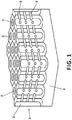
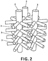
- Example 1 Relates to a porous alumina film - nanostructured material (1) of the invention - on a substrate (4), said film having at least one longitudinal pore (2), preferably several longitudinal pores (2) that emerge from said substrate (4) and having respective longitudinal axes essentially perpendicular to the substrate (4) and which are connected by at least one transverse pore (3), preferably various longitudinal axes (3) defined in periodically spaced planes, as can be observed in Figures 4a-4c , although in other possible embodiments, as can be observed in Figure 6 , the transverse pores (3) may be defined in planes having aperiodic distances therebetween, as will be seen in subsequent example.
- An aluminium wafer 1.6 cm diameter was firstly subjected to a cleaning process using acetone, water, isopropanol and ethanol sequentially.
- the clean aluminium wafer was subjected to an electrochemical polishing process in an electrolyte composed of HClO 4 :EtOH (1:3) at 20 V for 3 minutes.
- the wafer was subjected to a first anodizing reaction at a voltage of V AB , V 25, to form aluminium oxide film called alumina.
- This alumina layer was removed by dissolution in a mixture of phosphoric acid at 7% by weight and chromic oxide at 1.8% by weight for 24 hours at 25°C.
- the silicon wafer was subjected to a second anodizing process using pulse anodizing, which consisted of applying a constant voltage of 25 V for 180 s and a pulse at a nominal voltage of 32 V for 2 s.
- the second pulse anodizing process produced a growth of anodic alumina. This second anodizing process was maintained until the thickness of said layer was 20 ⁇ m.
- the alumina layer formed is subjected to a chemical attack process using H 3 PO 4 at 5% by weight at a temperature of 30 ° C for 18 minutes.
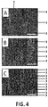
- the resulting anodic alumina film whose microstructure is shown in Figure 3a is characterized by having longitudinal pores (2) and transverse planes pores (3) resulting in the nanostructured material (1).
- the longitudinal pores (2) are characterised in that they have a hexagonal arrangement, a distance of 65 nm between first neighbours and a cross-section of 40 nm.
- Transverse pores (3) are characterised in that they have an elliptical section with an axis aligned parallel to the 35 nm longitudinal pores (2) and an axis aligned on the 25 nm transverse pore plane (3) (see Figure 3b ).
- Transverse pore planes (3) may have a periodic distance of approximately 320 nm (see Figure 3a ).
- the application time of the pulse anodizing process was maintained until reaching an anodized alumina film thickness of 200 ⁇ m.
- the anodized alumina film thus obtained has the same characteristics described above relating to the dimensions and the arrangement of the longitudinal pores (2) and transverse pores (3).
- Example 1 in the second anodizing process using pulse anodizing during the application of a constant voltage of 25 V between pulses at a nominal voltage of 32 V for 2 s, it was varied so that longer times between pulses increased the distance between the transverse pore planes (3) and shorter times decreased said distance.
- the distance between transverse pore planes (3) can be proportional to the time of application of the constant voltage between current-limited anodizing pulses.
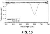
- the nanostructured material (1) of the invention and therefore the anodic alumina film, may exhibit a colour that is variable depending on the angle of incidence of light forming an interference colour.
- Example 2 porous alumina film with longitudinal pores (2) connected to aperiodically spaced transverse pore planes (3).
- the porous alumina material of Example 1 was processed following the process described in said Example No. 1, which was repeated during the pulse anodizing process modifying the application time at a constant voltage of 25 V between the current-limited anodizing pulses at a nominal voltage of 32 V.
- the resulting alumina film is characterised as shown in Figure 6 in that it has transverse pore planes (3) are aperiodically spaced.
- Example 3 Porous alumina film with longitudinal pores (2) connected to transverse pore planes (3) filled with polymeric material which is shown in Figures 7a and 7b .
- the porous alumina material of Example 1 was processed following the process described in said Example No. 1 and the three-dimensional pore lattice was filled following a process of infiltration of polymeric compounds, PFO-DTBT, P3EAT and PPV.
- the following solutions were prepared: PCDTBT 4g/L in chloroform, PFO-DTBT 4g/L in chloroform, P3EAT 4g/L in chloroform and PPV 4g/L in tetrahydrofuran.
- the anodized alumina films with three-dimensional porosity were immersed in each of the solutions for 10 minutes.
- the anodized alumina films with three-dimensional porosity were extracted and the solvent contained in their pores was left to dry in ambient conditions.
- the nanostructured material (1) and therefore, the porous alumina film with longitudinal pores (2) connected to transverse pore planes (3) filled with these polymeric materials may have luminescent properties that vary depending on the polymer used.
- the nanostructured porous alumina material (1) of Example 1 was processed following the process described in said Example 1 and the three-dimensional pore lattice was filled following a process of infiltration with polymeric compound of P(VDF-TrFE).
- the following solution was prepared: P(VDF-TrFE) 5% by weight of dimethylformamide.
- the AAO3D was immersed in the solution for 10 minutes.
- the anodized alumina film with three-dimensional porosity was extracted and the solvent contained in its pores was left to dry in ambient conditions.
- the porous alumina film with longitudinal pores (2) connected to transverse pore planes (3) filled with said polymeric materials has the advantage of having possess ferroelectric properties besides luminescent properties that also change with the angle of incidence of light.
- Example 4 Process for obtaining three-dimensional polymer nanowire lattices interconnected as shown in Figure 8 .
- the nanostructured porous alumina material (1) Example 1 was processed following the process described in said Example 1 and the three-dimensional pore lattice (2, 3) was filled with polystyrene following a process of in situ polymerisation.
- the styrene was polymerised within the three-dimensional alumina using AIBN as a primer in an atmosphere of N 2 for 1 hour.
- the nanostructured anodized alumina material (1) was selectively dissolved in a solution of 10 M NaOH for 60 minutes.
- a polypropylene nanowire lattice connected by transverse planes of polystyrene wires that connect the longitudinal wires through their first neighbours was obtained.
- Example 5 Process for obtaining three-dimensional lattices of interconnected Bi 2 Te 3 nanowires shown in Figure 9 .
- the three-dimensional nanostructured porous alumina material (1) of Example 1 was processed following the process described in said Example 1 and the three-dimensional pore lattice (2, 3) was filled with Bi2Te3, following an electrochemical deposition process.
- a metallic layer was deposited on one of the 3D alumina surfaces that served as an electrode. This deposited electrode was used as a cathode of an electrochemical cell.
- the growth of Bi 2 Te 3 inside the three-dimensional porous lattice in the anodic alumina was carried out by means of electrodeposition in a triple-electrode electrochemical cell for 8 hours. The conditions of the pulses were: 20 mV for 0.1 s and 0 mA/cm 2 for 0.1 s.
- the three-dimensional porous anodic alumina film thus obtained and filled by electrochemical deposition of Bi 2 Te 3 is characterised in that it is green as opposed to the colour of the compound Bi 2 Te 3 , which is dark grey.
Landscapes
- Chemical & Material Sciences (AREA)
- Engineering & Computer Science (AREA)
- Organic Chemistry (AREA)
- Materials Engineering (AREA)
- Chemical Kinetics & Catalysis (AREA)
- Metallurgy (AREA)
- Electrochemistry (AREA)
- Nanotechnology (AREA)
- General Physics & Mathematics (AREA)
- Physics & Mathematics (AREA)
- Condensed Matter Physics & Semiconductors (AREA)
- Crystallography & Structural Chemistry (AREA)
- Inorganic Chemistry (AREA)
- Composite Materials (AREA)
- Manufacturing & Machinery (AREA)
- General Chemical & Material Sciences (AREA)
- Life Sciences & Earth Sciences (AREA)
- Polymers & Plastics (AREA)
- Medicinal Chemistry (AREA)
- Health & Medical Sciences (AREA)
- Geology (AREA)
- Compounds Of Alkaline-Earth Elements, Aluminum Or Rare-Earth Metals (AREA)
Applications Claiming Priority (2)
| Application Number | Priority Date | Filing Date | Title |
|---|---|---|---|
| ES201431048A ES2559275B1 (es) | 2014-07-11 | 2014-07-11 | Material nanoestructurado, proceso de obtención y uso del mismo |
| PCT/ES2015/070519 WO2016005636A1 (es) | 2014-07-11 | 2015-07-02 | Material nanoestructurado, proceso de obtención y uso del mismo |
Publications (2)
| Publication Number | Publication Date |
|---|---|
| EP3168331A1 true EP3168331A1 (de) | 2017-05-17 |
| EP3168331A4 EP3168331A4 (de) | 2018-02-07 |
Family
ID=55063626
Family Applications (1)
| Application Number | Title | Priority Date | Filing Date |
|---|---|---|---|
| EP15818949.8A Withdrawn EP3168331A4 (de) | 2014-07-11 | 2015-07-02 | Nanostrukturiertes material, herstellungsverfahren und verwendung davon |
Country Status (5)
| Country | Link |
|---|---|
| US (1) | US20170221597A1 (de) |
| EP (1) | EP3168331A4 (de) |
| CN (1) | CN107002273A (de) |
| ES (1) | ES2559275B1 (de) |
| WO (1) | WO2016005636A1 (de) |
Families Citing this family (5)
| Publication number | Priority date | Publication date | Assignee | Title |
|---|---|---|---|---|
| CN111024257B (zh) * | 2019-09-29 | 2021-12-24 | 株洲国创轨道科技有限公司 | 一种超材料温度感知传感器、制备方法及其应用 |
| TW202212640A (zh) * | 2020-04-24 | 2022-04-01 | 紐西蘭商西洛斯材料科學有限公司 | 在合金上施加著色塗層的方法 |
| EP4379097A4 (de) * | 2021-11-08 | 2025-01-22 | Samsung Electronics Co., Ltd. | Anodisierbares blech aus aluminiumlegierung und verfahren zur herstellung davon |
| CN116646118B (zh) * | 2023-05-29 | 2023-12-22 | 重庆大学 | 一种用于高压裸线散热降温的氧化铝膜结构及制备方法 |
| CN120607272B (zh) * | 2025-08-11 | 2025-10-10 | 中国科学院合肥物质科学研究院 | 一种三维有序空心氧化亚铜纳米阵列及其制备方法及应用 |
Family Cites Families (4)
| Publication number | Priority date | Publication date | Assignee | Title |
|---|---|---|---|---|
| US20050276743A1 (en) * | 2004-01-13 | 2005-12-15 | Jeff Lacombe | Method for fabrication of porous metal templates and growth of carbon nanotubes and utilization thereof |
| CN100412237C (zh) * | 2005-03-18 | 2008-08-20 | 武汉大学 | 一种三维氧化铝纳米模板的制备方法 |
| EP1884578A1 (de) * | 2006-07-31 | 2008-02-06 | MPG Max-Planck-Gesellschaft zur Förderung der Wissenschaften e.V. | Verfahren zur Herstellung selbstordnender poröser Aluminastruktur, nanoporöser Artikel und Nanoobjekt. |
| JP5294048B2 (ja) * | 2007-12-05 | 2013-09-18 | 富士電機株式会社 | アルミナナノホールアレー及び磁気記録媒体の作製方法 |
-
2014
- 2014-07-11 ES ES201431048A patent/ES2559275B1/es not_active Expired - Fee Related
-
2015
- 2015-07-02 US US15/325,595 patent/US20170221597A1/en not_active Abandoned
- 2015-07-02 CN CN201580049171.6A patent/CN107002273A/zh active Pending
- 2015-07-02 EP EP15818949.8A patent/EP3168331A4/de not_active Withdrawn
- 2015-07-02 WO PCT/ES2015/070519 patent/WO2016005636A1/es not_active Ceased
Also Published As
| Publication number | Publication date |
|---|---|
| CN107002273A (zh) | 2017-08-01 |
| WO2016005636A1 (es) | 2016-01-14 |
| ES2559275B1 (es) | 2016-11-22 |
| EP3168331A4 (de) | 2018-02-07 |
| US20170221597A1 (en) | 2017-08-03 |
| ES2559275A1 (es) | 2016-02-11 |
Similar Documents
| Publication | Publication Date | Title |
|---|---|---|
| EP3168331A1 (de) | Nanostrukturiertes material, herstellungsverfahren und verwendung davon | |
| Sulka et al. | Through-hole membranes of nanoporous alumina formed by anodizing in oxalic acid and their applications in fabrication of nanowire arrays | |
| CN101698961B (zh) | 一种表面等离激元晶体的制备方法 | |
| Kondo et al. | Ideally ordered porous TiO2 prepared by anodization of pretextured Ti by nanoimprinting process | |
| EP2367969A1 (de) | Herstellung von nanoporösen materialien | |
| US20180208467A1 (en) | Three-dimensional deterministic graphene architectures formed using three-dimensional templates | |
| Stępniowski et al. | Fabrication and geometric characterization of highly-ordered hexagonally arranged arrays of nanoporous anodic alumina | |
| Kaniukov et al. | Electrochemically deposited copper nanotubes | |
| Mebed et al. | Electrochemical fabrication of 2D and 3D nickel nanowires using porous anodic alumina templates | |
| Resende et al. | Sub-10 nm porous alumina templates to produce sub-10 nm nanowires | |
| Albu et al. | TiO2 nanotube layers: Flexible and electrically active flow-through membranes | |
| US20080085364A1 (en) | Process For Producing Nanoparticle Or Nanostructure With Use Of Nanoporous Material | |
| Yin et al. | Fabrication of anodic aluminium oxide templates on curved surfaces | |
| Jeong et al. | Three-dimensional (3D) anodic aluminum surfaces by modulating electrochemical method | |
| Kalska-Szostko | Electrochemical methods in nanomaterials preparation | |
| US20180371631A1 (en) | Exposed segmented nanostructure arrays | |
| Kanchibotla et al. | Self assembly of nanostructures using nanoporous alumina templates | |
| Yadav et al. | Controlled growth of highly aligned Cu nanowires by pulse electrodeposition in nanoporous alumina | |
| Kotha et al. | Nanowire Fabrication in Porous Alumina Tempalets Produced by Employing Sulphuric, Oxalic and Phosphoric Acids | |
| Yi et al. | Mechanically robust and thermally conductive nano-porous anodic aluminum oxide templates via thermal stress minimization and alpha phase transformation for interposer | |
| Chahrour et al. | Influence of the Voltage on Pore Diameter and Growth Rate of Thin Anodic Aluminium Oxide (AAO) Pattern on Silicon Substrate | |
| Guo et al. | Preparation and dispersion of Ni–Cu composite nanoparticles | |
| KR101479211B1 (ko) | 알루미늄의 전기화학적 고온 양극 산화를 통한 극미세 나노 다공성 알루미나 구조체의 제조 방법 | |
| Boominatha Sellarajan et al. | Synthesis of highly ordered nanoporous anodic aluminium oxide templates and template-based nanomaterials | |
| KR100619354B1 (ko) | 양극산화알루미늄 템플레이트를 이용한 나노 입상 필터 및그 제조방법 |
Legal Events
| Date | Code | Title | Description |
|---|---|---|---|
| STAA | Information on the status of an ep patent application or granted ep patent |
Free format text: STATUS: THE INTERNATIONAL PUBLICATION HAS BEEN MADE |
|
| PUAI | Public reference made under article 153(3) epc to a published international application that has entered the european phase |
Free format text: ORIGINAL CODE: 0009012 |
|
| STAA | Information on the status of an ep patent application or granted ep patent |
Free format text: STATUS: REQUEST FOR EXAMINATION WAS MADE |
|
| 17P | Request for examination filed |
Effective date: 20170213 |
|
| AK | Designated contracting states |
Kind code of ref document: A1 Designated state(s): AL AT BE BG CH CY CZ DE DK EE ES FI FR GB GR HR HU IE IS IT LI LT LU LV MC MK MT NL NO PL PT RO RS SE SI SK SM TR |
|
| AX | Request for extension of the european patent |
Extension state: BA ME |
|
| DAV | Request for validation of the european patent (deleted) | ||
| DAX | Request for extension of the european patent (deleted) | ||
| A4 | Supplementary search report drawn up and despatched |
Effective date: 20180109 |
|
| RIC1 | Information provided on ipc code assigned before grant |
Ipc: C25D 11/12 20060101ALI20180103BHEP Ipc: C25D 11/16 20060101ALI20180103BHEP Ipc: C25D 11/04 20060101ALI20180103BHEP Ipc: B82Y 30/00 20110101ALI20180103BHEP Ipc: C25D 11/02 20060101ALI20180103BHEP Ipc: C25D 11/24 20060101ALI20180103BHEP Ipc: C25D 11/08 20060101AFI20180103BHEP Ipc: B82Y 40/00 20110101ALI20180103BHEP |
|
| STAA | Information on the status of an ep patent application or granted ep patent |
Free format text: STATUS: THE APPLICATION IS DEEMED TO BE WITHDRAWN |
|
| 18D | Application deemed to be withdrawn |
Effective date: 20180807 |