EP3167478B1 - Insulating liner for a through-body via and corresponding method of deposition - Google Patents
Insulating liner for a through-body via and corresponding method of deposition Download PDFInfo
- Publication number
- EP3167478B1 EP3167478B1 EP14896984.3A EP14896984A EP3167478B1 EP 3167478 B1 EP3167478 B1 EP 3167478B1 EP 14896984 A EP14896984 A EP 14896984A EP 3167478 B1 EP3167478 B1 EP 3167478B1
- Authority
- EP
- European Patent Office
- Prior art keywords
- insulation layers
- oxide
- integrated circuit
- liner
- semiconductor structure
- Prior art date
- Legal status (The legal status is an assumption and is not a legal conclusion. Google has not performed a legal analysis and makes no representation as to the accuracy of the status listed.)
- Active
Links
Images


Classifications
-
- H—ELECTRICITY
- H10—SEMICONDUCTOR DEVICES; ELECTRIC SOLID-STATE DEVICES NOT OTHERWISE PROVIDED FOR
- H10W—GENERIC PACKAGES, INTERCONNECTIONS, CONNECTORS OR OTHER CONSTRUCTIONAL DETAILS OF DEVICES COVERED BY CLASS H10
- H10W42/00—Arrangements for protection of devices
- H10W42/121—Arrangements for protection of devices protecting against mechanical damage
-
- H—ELECTRICITY
- H10—SEMICONDUCTOR DEVICES; ELECTRIC SOLID-STATE DEVICES NOT OTHERWISE PROVIDED FOR
- H10D—INORGANIC ELECTRIC SEMICONDUCTOR DEVICES
- H10D62/00—Semiconductor bodies, or regions thereof, of devices having potential barriers
- H10D62/10—Shapes, relative sizes or dispositions of the regions of the semiconductor bodies; Shapes of the semiconductor bodies
- H10D62/113—Isolations within a component, i.e. internal isolations
- H10D62/115—Dielectric isolations, e.g. air gaps
-
- H—ELECTRICITY
- H10—SEMICONDUCTOR DEVICES; ELECTRIC SOLID-STATE DEVICES NOT OTHERWISE PROVIDED FOR
- H10W—GENERIC PACKAGES, INTERCONNECTIONS, CONNECTORS OR OTHER CONSTRUCTIONAL DETAILS OF DEVICES COVERED BY CLASS H10
- H10W10/00—Isolation regions in semiconductor bodies between components of integrated devices
- H10W10/01—Manufacture or treatment
- H10W10/011—Manufacture or treatment of isolation regions comprising dielectric materials
- H10W10/014—Manufacture or treatment of isolation regions comprising dielectric materials using trench refilling with dielectric materials, e.g. shallow trench isolations
- H10W10/0143—Manufacture or treatment of isolation regions comprising dielectric materials using trench refilling with dielectric materials, e.g. shallow trench isolations comprising concurrently refilling multiple trenches having different shapes or dimensions
-
- H—ELECTRICITY
- H10—SEMICONDUCTOR DEVICES; ELECTRIC SOLID-STATE DEVICES NOT OTHERWISE PROVIDED FOR
- H10W—GENERIC PACKAGES, INTERCONNECTIONS, CONNECTORS OR OTHER CONSTRUCTIONAL DETAILS OF DEVICES COVERED BY CLASS H10
- H10W10/00—Isolation regions in semiconductor bodies between components of integrated devices
- H10W10/10—Isolation regions comprising dielectric materials
- H10W10/17—Isolation regions comprising dielectric materials formed using trench refilling with dielectric materials, e.g. shallow trench isolations
-
- H—ELECTRICITY
- H10—SEMICONDUCTOR DEVICES; ELECTRIC SOLID-STATE DEVICES NOT OTHERWISE PROVIDED FOR
- H10W—GENERIC PACKAGES, INTERCONNECTIONS, CONNECTORS OR OTHER CONSTRUCTIONAL DETAILS OF DEVICES COVERED BY CLASS H10
- H10W20/00—Interconnections in chips, wafers or substrates
- H10W20/01—Manufacture or treatment
- H10W20/021—Manufacture or treatment of interconnections within wafers or substrates
- H10W20/023—Manufacture or treatment of interconnections within wafers or substrates the interconnections being through-semiconductor vias
- H10W20/0265—Manufacture or treatment of interconnections within wafers or substrates the interconnections being through-semiconductor vias characterised by the sidewall insulation
-
- H—ELECTRICITY
- H10—SEMICONDUCTOR DEVICES; ELECTRIC SOLID-STATE DEVICES NOT OTHERWISE PROVIDED FOR
- H10W—GENERIC PACKAGES, INTERCONNECTIONS, CONNECTORS OR OTHER CONSTRUCTIONAL DETAILS OF DEVICES COVERED BY CLASS H10
- H10W20/00—Interconnections in chips, wafers or substrates
- H10W20/01—Manufacture or treatment
- H10W20/031—Manufacture or treatment of conductive parts of the interconnections
- H10W20/069—Manufacture or treatment of conductive parts of the interconnections by forming self-aligned vias or self-aligned contact plugs
-
- H—ELECTRICITY
- H10—SEMICONDUCTOR DEVICES; ELECTRIC SOLID-STATE DEVICES NOT OTHERWISE PROVIDED FOR
- H10W—GENERIC PACKAGES, INTERCONNECTIONS, CONNECTORS OR OTHER CONSTRUCTIONAL DETAILS OF DEVICES COVERED BY CLASS H10
- H10W20/00—Interconnections in chips, wafers or substrates
- H10W20/01—Manufacture or treatment
- H10W20/071—Manufacture or treatment of dielectric parts thereof
- H10W20/074—Manufacture or treatment of dielectric parts thereof of dielectric parts comprising thin functional dielectric layers, e.g. dielectric etch-stop, barrier, capping or liner layers
- H10W20/075—Manufacture or treatment of dielectric parts thereof of dielectric parts comprising thin functional dielectric layers, e.g. dielectric etch-stop, barrier, capping or liner layers of multilayered thin functional dielectric layers
-
- H—ELECTRICITY
- H10—SEMICONDUCTOR DEVICES; ELECTRIC SOLID-STATE DEVICES NOT OTHERWISE PROVIDED FOR
- H10W—GENERIC PACKAGES, INTERCONNECTIONS, CONNECTORS OR OTHER CONSTRUCTIONAL DETAILS OF DEVICES COVERED BY CLASS H10
- H10W20/00—Interconnections in chips, wafers or substrates
- H10W20/20—Interconnections within wafers or substrates, e.g. through-silicon vias [TSV]
-
- H—ELECTRICITY
- H10—SEMICONDUCTOR DEVICES; ELECTRIC SOLID-STATE DEVICES NOT OTHERWISE PROVIDED FOR
- H10W—GENERIC PACKAGES, INTERCONNECTIONS, CONNECTORS OR OTHER CONSTRUCTIONAL DETAILS OF DEVICES COVERED BY CLASS H10
- H10W20/00—Interconnections in chips, wafers or substrates
- H10W20/40—Interconnections external to wafers or substrates, e.g. back-end-of-line [BEOL] metallisations or vias connecting to gate electrodes
- H10W20/41—Interconnections external to wafers or substrates, e.g. back-end-of-line [BEOL] metallisations or vias connecting to gate electrodes characterised by their conductive parts
- H10W20/425—Barrier, adhesion or liner layers
-
- H—ELECTRICITY
- H10—SEMICONDUCTOR DEVICES; ELECTRIC SOLID-STATE DEVICES NOT OTHERWISE PROVIDED FOR
- H10W—GENERIC PACKAGES, INTERCONNECTIONS, CONNECTORS OR OTHER CONSTRUCTIONAL DETAILS OF DEVICES COVERED BY CLASS H10
- H10W20/00—Interconnections in chips, wafers or substrates
- H10W20/40—Interconnections external to wafers or substrates, e.g. back-end-of-line [BEOL] metallisations or vias connecting to gate electrodes
- H10W20/45—Interconnections external to wafers or substrates, e.g. back-end-of-line [BEOL] metallisations or vias connecting to gate electrodes characterised by their insulating parts
- H10W20/47—Interconnections external to wafers or substrates, e.g. back-end-of-line [BEOL] metallisations or vias connecting to gate electrodes characterised by their insulating parts comprising two or more dielectric layers having different properties, e.g. different dielectric constants
-
- H—ELECTRICITY
- H10—SEMICONDUCTOR DEVICES; ELECTRIC SOLID-STATE DEVICES NOT OTHERWISE PROVIDED FOR
- H10W—GENERIC PACKAGES, INTERCONNECTIONS, CONNECTORS OR OTHER CONSTRUCTIONAL DETAILS OF DEVICES COVERED BY CLASS H10
- H10W72/00—Interconnections or connectors in packages
- H10W72/90—Bond pads, in general
-
- H—ELECTRICITY
- H10—SEMICONDUCTOR DEVICES; ELECTRIC SOLID-STATE DEVICES NOT OTHERWISE PROVIDED FOR
- H10W—GENERIC PACKAGES, INTERCONNECTIONS, CONNECTORS OR OTHER CONSTRUCTIONAL DETAILS OF DEVICES COVERED BY CLASS H10
- H10W20/00—Interconnections in chips, wafers or substrates
- H10W20/01—Manufacture or treatment
- H10W20/071—Manufacture or treatment of dielectric parts thereof
- H10W20/074—Manufacture or treatment of dielectric parts thereof of dielectric parts comprising thin functional dielectric layers, e.g. dielectric etch-stop, barrier, capping or liner layers
- H10W20/076—Manufacture or treatment of dielectric parts thereof of dielectric parts comprising thin functional dielectric layers, e.g. dielectric etch-stop, barrier, capping or liner layers in via holes or trenches
-
- H—ELECTRICITY
- H10—SEMICONDUCTOR DEVICES; ELECTRIC SOLID-STATE DEVICES NOT OTHERWISE PROVIDED FOR
- H10W—GENERIC PACKAGES, INTERCONNECTIONS, CONNECTORS OR OTHER CONSTRUCTIONAL DETAILS OF DEVICES COVERED BY CLASS H10
- H10W72/00—Interconnections or connectors in packages
- H10W72/20—Bump connectors, e.g. solder bumps or copper pillars; Dummy bumps; Thermal bumps
- H10W72/29—Bond pads specially adapted therefor
-
- H—ELECTRICITY
- H10—SEMICONDUCTOR DEVICES; ELECTRIC SOLID-STATE DEVICES NOT OTHERWISE PROVIDED FOR
- H10W—GENERIC PACKAGES, INTERCONNECTIONS, CONNECTORS OR OTHER CONSTRUCTIONAL DETAILS OF DEVICES COVERED BY CLASS H10
- H10W72/00—Interconnections or connectors in packages
- H10W72/90—Bond pads, in general
- H10W72/921—Structures or relative sizes of bond pads
- H10W72/923—Bond pads having multiple stacked layers
-
- H—ELECTRICITY
- H10—SEMICONDUCTOR DEVICES; ELECTRIC SOLID-STATE DEVICES NOT OTHERWISE PROVIDED FOR
- H10W—GENERIC PACKAGES, INTERCONNECTIONS, CONNECTORS OR OTHER CONSTRUCTIONAL DETAILS OF DEVICES COVERED BY CLASS H10
- H10W72/00—Interconnections or connectors in packages
- H10W72/90—Bond pads, in general
- H10W72/941—Dispositions of bond pads
- H10W72/942—Dispositions of bond pads relative to underlying supporting features, e.g. bond pads, RDLs or vias
Definitions
- the present disclosure relates to integrated circuits, and more particularly, to liners for through- silicon vias or other through-body via structures.
- a through-silicon via is an electrically conductive connection that passes through a silicon substrate.
- TSV interconnections can be used with three-dimensional system-in-packaging (3D-SiP) technology, which permits short connection distances and fast speeds between devices.
- TSVs can be formed by depositing a conductive material, such as copper, into openings etched in the substrate.
- a non-conductive layer between the silicon and the conductive material also referred to as a TSV liner, serves as an insulator.
- the aspect ratio of the TSV opening i.e., height to width
- the liner deposition process on a chemical vapor deposition (CVD) platform involves deposition of a tensile thermal film followed by plasma assisted hermetic compressive oxide film as a cap.
- CVD chemical vapor deposition
- US 2014/015146 A1 discloses a semiconductor component comprising: semiconductor substrate having an opening; a first dielectric liner having a first stress disposed over an interior surface of the opening; a second dielectric liner having a second stress disposed over the first dielectric liner, wherein a direction of the first stress is opposite a direction of the second stress; and a conductive material disposed over the second dielectric liner.
- an integrated circuit includes a silicon semiconductor substrate having one or more through-silicon vias (TSVs), although other through-body vias can be used as will be appreciated in light of this disclosure.
- TSVs through-silicon vias
- Each TSV extends through at least a portion of the substrate, for example, from one side (e.g., top) of the substrate to the opposite side of the substrate (e.g., bottom), or from one internal layer of the substrate to another internal layer.
- a liner is disposed between the substrate and each TSV.
- the liner is formed of multiple alternating layers of dissimilar insulation films (e.g., tensile films and compressive films) sandwiched together.
- the liner can be formed by depositing two or more 0.5x thickness thermal layers and two or more 0.5x thickness compressive layers in alternating succession.
- stress can be relieved in the liner, which reduces or eliminates defects such as cracks or seams at the bottom corner of the via.
- the techniques can be embodied, for example, in discrete memory devices (e.g., non-volatile and volatile memory chips), integrated system designs (e.g., purpose-built silicon), or on-chip memory (e.g., microprocessor with on-chip non-volatile cache), to name a few. Numerous other embodiments, variations, and applications will be apparent in light of this disclosure.
- a TSV liner is deposited after the via has been etched into the silicon substrate to electrically insulate the conductor in the via from the silicon.
- the liner deposition process on a chemical vapor deposition (CVD) platform can involve deposition of a tensile thermal film followed by plasma assisted hermetic compressive oxide film as a cap. This approach can lead to cracks or seams between the TSV and the bottom corner of the via due to stress mismatch and inherent tensile stress in the thermal film caused by a high deposition rate or a high thickness of the liner.
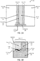
- Figure 1A shows a partial cross-section of an IC 100 in which a substrate 102 is insulated from a via 104 by a liner 110 having a tensile film layer 112 and a compressive film layer 114.
- Figure 1B is a detailed view of a portion of the IC 100 where the liner 110 is landed on a landing pad 106.
- the tensile film 112 when deposited in the manner illustrated in Figures 1A and 1B , can develop a crack 120 or seam at the corner 122 of the via 104 and the substrate 102 due to inherent stress in the liner 110 caused by a high deposition rate or the thickness of the liner. This crack 120 or seam can provide an undesirable leakage path between the via 104 and the substrate 102.
- a TSV liner structure and TSV liner deposition process that can reduce such leakage paths for meeting the functional specifications of the IC using a sandwich approach in which the tensile and compressive films are deposited alternately.
- the stress in the liner can be relieved.
- imaging techniques e.g., transmission electron microscopy or TEM
- TSV liner having alternating layers can be realized by, for example, changing the number of layers (e.g., four, six, etc.) depending on the desired total thickness of the liner so as to keep the individual layers thin enough to avoid stress-induced cracks or seams in the liner.
- the structures and techniques described herein can be used in numerous applications, such as discrete memory devices as well as in microprocessors or other on-chip applications. Other suitable applications will be apparent in light of this disclosure. It will be further understood that the techniques described herein can be used with any type of through-body via structure and are not limited to silicon.
- FIG. 2 illustrates a cross-section of a portion of an integrated circuit (IC) 200 configured in accordance with an embodiment of the present disclosure.
- the IC 200 includes a substrate 202 and a TSV 204 extending through the substrate 202.
- the TSV 204 can be filled with a conductive material, such as copper.
- a conductive material such as copper.
- the IC 200 may, in some embodiments, include a landing pad 206 or other surface disposed at one or both ends of the TSV 204, depending on the particular application.
- One or more TSV liners 210 are disposed between a sidewall of the substrate 202 and the via 204. In embodiments having the landing pad 206, a portion of the TSV liner 210 abuts the landing pad 206, as shown in Figure 2 .
- the TSV liner 210 can be fabricated of materials that electrically insulate the conductive material in the via 204 from the substrate 202.
- the TSV liner 210 includes alternating layers of dielectric film layers formed using different deposition materials or methods.
- the dielectric film layers may be formed using one or more types of oxide, nitride and carbide films, such as silicon oxide, silicon nitride, silicon carbide, carbon doped oxide (CDO), oxide doped carbide, hafnium oxide, hafnium silicon oxide, lanthanum oxide, lanthanum aluminum oxide, zirconium oxide, zirconium silicon oxide, tantalum oxide, titanium oxide, barium strontium titanium oxide, barium titanium oxide, strontium titanium oxide, yttrium oxide, aluminum oxide, and lead scandium tantalum oxide, or other dielectric films that can conform to large or the otherwise given aspect ratios.
- oxide, nitride and carbide films such as silicon oxide, silicon nitride, silicon carbide, carbon doped oxide (CDO), oxide doped carbide, hafnium oxide, hafnium silicon oxide, lanthanum oxide, lanthanum aluminum oxide, zirconium oxide, zirconium silicon oxide, tantalum oxide, titanium oxide, barium strontium
- the TSV liner 210 includes a first insulation layer 212, a second insulation layer 214, a third insulation layer 216, and a fourth insulation layer 218.
- the first and third insulation layers 212, 216 are oxide, nitride or carbide films (or other suitable insulator materials) having an inherent tensile stress
- the second and fourth insulation layers 214, 218 are oxide, nitride or carbide films (or other suitable insulator materials) having an inherent compressive stress.
- the TSV liner 210 can be formed by a variety of deposition techniques. The stress of the films in any layer can be modulated by process parameters during deposition.
- the first and third insulation layers 212, 216 can be films having an inherent compressive stress
- the second and fourth insulation layers 214, 218 can be films having an inherent tensile stress.
- the deposition of the first and third insulation layers 212, 216 can be carried out using a thermal oxidation process
- the deposition of the second and fourth insulation layers 214, 218 can be carried out using a plasma-enhanced chemical vapor deposition (PECVD) process.
- PECVD plasma-enhanced chemical vapor deposition
- the first and third insulation layers 212, 216 can have different structural properties than the second and fourth insulation layers 214, 218.
- the stress of each layer can be changed from compressive to tensile or from tensile to compressive by modulating high and low frequency power from generators.
- the stress of each layer can be changed from compressive to tensile or from tensile to compressive by modulating the ratio of materials in the insulator compound, such as in the case of Si to N (for silicon nitride films) or Si to O (for silicon dioxide films).
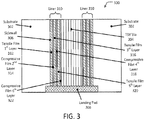
- FIG 3 illustrates a cross-section of a portion of an IC 300 configured in accordance with another embodiment of the present disclosure.
- the IC 300 includes a substrate 302 and a TSV 304 extending through the substrate 302.
- the TSV 304 can be filled with a conductive material, such as copper. Although only one TSV is depicted in Figure 3 , it will be understood that the IC 300 can be configured to have any number of TSVs.
- the IC 300 may, in some embodiments, include a landing pad 306 or other surface disposed at one or both ends of the TSV 304, depending on the particular application.
- One or more TSV liners 310 are disposed between a sidewall of the substrate 302 and the via 304. In embodiments having the landing pad 306, a portion of the TSV liner 210 abuts the landing pad 306, as shown in Figure 3 .
- the TSV liner 310 can be fabricated of materials that electrically insulate the conductive material in the via 204 from the substrate 302.
- the TSV liner 310 includes alternating layers of dielectric film layers formed using different deposition materials or methods.
- the dielectric film layers may be formed using one or more types of oxide, nitride and carbide films, such as silicon oxide, silicon nitride, or other dielectric films that can conform to large aspect ratios, as previously explained.
- the TSV liner 310 includes a first insulation layer 312, a second insulation layer 314, a third insulation layer 316, a fourth insulation layer 318, a fifth insulation layer 320, and a sixth insulation layer 322.
- the first, third and fifth insulation layers 312, 316, 320 can include, for example, an oxide or nitride or other insulator film having an inherent tensile stress (e.g., silicon dioxide), and the second, fourth and sixth insulation layers 314, 318, 322 can include an oxide or nitride or other insulator film having an inherent compressive stress (e.g., silicon nitride).
- the TSV liner 310 can be formed by a variety of deposition techniques.
- the deposition of the first, third and fifth insulation layers 312, 316, 320 can be carried out using a thermal oxidation process, and the deposition of the second, fourth and sixth insulation layers 314, 318, 322 can be carried out using a plasma-enhanced chemical vapor deposition (PECVD) process.
- PECVD plasma-enhanced chemical vapor deposition
- the first, third and fifth insulation layers 312, 316, 320 can have different structural properties than the second, fourth and sixth insulation layers 314, 318, 322. Example processes for forming these structures will be discussed with reference to Figure 4 .
- TSV liners can be fabricated with any number of insulation layers in arrangements similar to those described in this disclosure.
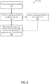
- FIG. 4 illustrates a methodology 400 for making an integrated circuit configured in accordance with an embodiment of the present disclosure.
- the method includes providing 402 a semiconductor substrate and forming 404 a through-silicon via (TSV) through the substrate.
- TSV through-silicon via
- the method 400 includes depositing 406 a landing pad adjacent to one end of the TSV. In other embodiments, the landing pad may not be needed.
- the method 400 continues by alternately depositing 408 each of a plurality of first insulation layers and a plurality of second insulation layers between the substrate and the TSV, thereby forming a liner for electrically insulating the TSV from the substrate.
- the first insulation layers have an inherent tensile stress and the second insulation layers have an inherent compressive stress.
- one of the first insulation layers is deposited adjacent to the substrate and one of the second insulation layers is deposited adjacent to the TSV.
- each of the first insulation layers is deposited using a thermal oxidation process.
- each of the second insulation layers is deposited using a plasma enhanced chemical vapor deposition (PECVD) process.
- PECVD plasma enhanced chemical vapor deposition
- all of the first insulation layers have substantially the same thickness.
- all of the second insulation layers have substantially the same thickness.
- all of the first and second insulation layers have substantially the same thickness.
- FIG. 5 illustrates a computing system implemented with an integrated circuit configured in accordance with an embodiment of the present disclosure.
- the computing system 500 houses a motherboard 502.
- the motherboard 502 may include a number of components, including, but not limited to, a processor 504 and at least one communication chip 506, each of which can be physically and electrically coupled to the motherboard 502, or otherwise integrated therein.
- the motherboard 502 may be, for example, any printed circuit board, whether a main board, a daughterboard mounted on a main board, or the only board of system 500, etc.
- computing system 500 may include one or more other components that may or may not be physically and electrically coupled to the motherboard 502.
- These other components may include, but are not limited to, volatile memory (e.g., DRAM), non-volatile memory (e.g., ROM), a graphics processor, a digital signal processor, a crypto processor, a chipset, an antenna, a display, a touchscreen display, a touchscreen controller, a battery, an audio codec, a video codec, a power amplifier, a global positioning system (GPS) device, a compass, an accelerometer, a gyroscope, a speaker, a camera, and a mass storage device (such as hard disk drive, compact disk (CD), digital versatile disk (DVD), and so forth).
- volatile memory e.g., DRAM
- non-volatile memory e.g., ROM
- a graphics processor e.g., a digital signal processor, a crypto processor, a chipset, an antenna, a display, a touchscreen display, a touchscreen controller, a battery, an audio codec, a video codec,
- the communication chip 506 enables wireless communications for the transfer of data to and from the computing system 500.
- wireless and its derivatives may be used to describe circuits, devices, systems, methods, techniques, communications channels, etc., that may communicate data through the use of modulated electromagnetic radiation through a non-solid medium. The term does not imply that the associated devices do not contain any wires, although in some embodiments they might not.
- the communication chip 506 may implement any of a number of wireless standards or protocols, including, but not limited to, Wi-Fi (IEEE 802.11 family), WiMAX (IEEE 802.16 family), IEEE 802.20, long term evolution (LTE), Ev-DO, HSPA+, HSDPA+, HSUPA+, EDGE, GSM, GPRS, CDMA, TDMA, DECT, Bluetooth, derivatives thereof, as well as any other wireless protocols that are designated as 3G, 4G, 5G, and beyond.
- the computing system 500 may include a plurality of communication chips 506.
- a first communication chip 506 may be dedicated to shorter range wireless communications such as Wi-Fi and Bluetooth and a second communication chip 506 may be dedicated to longer range wireless communications such as GPS, EDGE, GPRS, CDMA, WiMAX, LTE, Ev-DO, and others.
- the processor 504 of the computing system 500 includes an integrated circuit die packaged within the processor 504.
- the integrated circuit die of the processor includes onboard circuitry that is implemented with one or more integrated circuit structures or devices as variously described herein.
- the term "processor" may refer to any device or portion of a device that processes, for instance, electronic data from registers and/or memory to transform that electronic data into other electronic data that may be stored in registers and/or memory.
- the communication chip 506 also may include an integrated circuit die packaged within the communication chip 506.
- the integrated circuit die of the communication chip includes one or more integrated circuit structures or devices as described herein.
- multi-standard wireless capability may be integrated directly into the processor 504 (e.g., where functionality of any chips 506 is integrated into processor 504, rather than having separate communication chips).
- processor 504 may be a chip set having such wireless capability.
- any number of processor 504 and/or communication chips 506 can be used.
- any one chip or chip set can have multiple functions integrated therein.
- the computing device 500 may be a laptop, a netbook, a notebook, a smartphone, a tablet, a personal digital assistant (PDA), an ultra-mobile PC, a mobile phone, a desktop computer, a server, a printer, a scanner, a monitor, a set-top box, an entertainment control unit, a digital camera, a portable music player, a digital video recorder, or any other electronic device that processes data or employs one or more integrated circuit structures or devices, as variously described herein.
- PDA personal digital assistant
Landscapes
- Internal Circuitry In Semiconductor Integrated Circuit Devices (AREA)
- Formation Of Insulating Films (AREA)
Description
- The present disclosure relates to integrated circuits, and more particularly, to liners for through- silicon vias or other through-body via structures.
- A through-silicon via (TSV) is an electrically conductive connection that passes through a silicon substrate. TSV interconnections can be used with three-dimensional system-in-packaging (3D-SiP) technology, which permits short connection distances and fast speeds between devices. TSVs can be formed by depositing a conductive material, such as copper, into openings etched in the substrate. A non-conductive layer between the silicon and the conductive material, also referred to as a TSV liner, serves as an insulator. The aspect ratio of the TSV opening (i.e., height to width) is often high, e.g., 12: 1, increasing the difficulty of forming the liner. The liner deposition process on a chemical vapor deposition (CVD) platform involves deposition of a tensile thermal film followed by plasma assisted hermetic compressive oxide film as a cap.
-
US 2014/015146 A1 discloses a semiconductor component comprising: semiconductor substrate having an opening; a first dielectric liner having a first stress disposed over an interior surface of the opening; a second dielectric liner having a second stress disposed over the first dielectric liner, wherein a direction of the first stress is opposite a direction of the second stress; and a conductive material disposed over the second dielectric liner. -
-
Figure 1 A illustrates a partial cross-section of a typical TSV structure. - Figure IB illustrates a detailed view of a portion of the TSV structure of
Figure 1A . -
Figure 2 illustrates a cross-section of a portion of a TSV structure configured in accordance with an embodiment of the present disclosure. -
Figure 3 illustrates a cross-section of a portion of a TSV structure configured in accordance with an embodiment of the present disclosure. -
Figure 4 illustrates a methodology for making a TSV structure configured in accordance with an embodiment of the present disclosure. -
Figure 5 illustrates a computing system implemented with a TSV structure configured in accordance with an embodiment of the present disclosure. - Techniques are disclosed for through-body via liner structures and processes of forming such liner structures in an integrated circuit. In an embodiment, an integrated circuit includes a silicon semiconductor substrate having one or more through-silicon vias (TSVs), although other through-body vias can be used as will be appreciated in light of this disclosure. Each TSV extends through at least a portion of the substrate, for example, from one side (e.g., top) of the substrate to the opposite side of the substrate (e.g., bottom), or from one internal layer of the substrate to another internal layer. A liner is disposed between the substrate and each TSV. The liner is formed of multiple alternating layers of dissimilar insulation films (e.g., tensile films and compressive films) sandwiched together. For example, the liner can be formed by depositing two or more 0.5x thickness thermal layers and two or more 0.5x thickness compressive layers in alternating succession. As will be further appreciated in light of this disclosure, by using an approach in which the tensile and compressive films are alternately deposited, stress can be relieved in the liner, which reduces or eliminates defects such as cracks or seams at the bottom corner of the via. The techniques can be embodied, for example, in discrete memory devices (e.g., non-volatile and volatile memory chips), integrated system designs (e.g., purpose-built silicon), or on-chip memory (e.g., microprocessor with on-chip non-volatile cache), to name a few. Numerous other embodiments, variations, and applications will be apparent in light of this disclosure.
- Typically, during the manufacturing process of an integrated circuit (IC) having a TSV interconnection, a TSV liner is deposited after the via has been etched into the silicon substrate to electrically insulate the conductor in the via from the silicon. As noted above, the liner deposition process on a chemical vapor deposition (CVD) platform can involve deposition of a tensile thermal film followed by plasma assisted hermetic compressive oxide film as a cap. This approach can lead to cracks or seams between the TSV and the bottom corner of the via due to stress mismatch and inherent tensile stress in the thermal film caused by a high deposition rate or a high thickness of the liner. The cracks or seams can provide a leakage path, and become worse during the annealing process, potentially leading to two-to-three orders of magnitude increase in leakage. In more detail,
Figure 1A shows a partial cross-section of anIC 100 in which asubstrate 102 is insulated from avia 104 by aliner 110 having atensile film layer 112 and acompressive film layer 114.Figure 1B is a detailed view of a portion of theIC 100 where theliner 110 is landed on alanding pad 106. Thetensile film 112, when deposited in the manner illustrated inFigures 1A and 1B , can develop acrack 120 or seam at thecorner 122 of thevia 104 and thesubstrate 102 due to inherent stress in theliner 110 caused by a high deposition rate or the thickness of the liner. Thiscrack 120 or seam can provide an undesirable leakage path between thevia 104 and thesubstrate 102. - Thus, and in accordance with an embodiment of the present disclosure, a TSV liner structure and TSV liner deposition process that can reduce such leakage paths for meeting the functional specifications of the IC using a sandwich approach in which the tensile and compressive films are deposited alternately. By implementing the TSV liner layers in alternating fashion, particularly where each layer is deposited in thin layers, the stress in the liner can be relieved. Use of the disclosed structures and techniques can be identified cross-sectionally with imaging techniques (e.g., transmission electron microscopy or TEM) of a given integrated circuit or other device that has a liner structure that uses alternating layers of dissimilar structures, as variously described in this disclosure. For example, using TEM imaging, there will be observable differences in density, refractive index, modulus/hardness, and dielectric constant between a thermal dielectric film layer and a plasma-enhanced chemical vapor deposition (PECVD) dielectric film layer.
- Numerous embodiments and configurations that use a TSV liner having alternating layers can be realized by, for example, changing the number of layers (e.g., four, six, etc.) depending on the desired total thickness of the liner so as to keep the individual layers thin enough to avoid stress-induced cracks or seams in the liner. The structures and techniques described herein can be used in numerous applications, such as discrete memory devices as well as in microprocessors or other on-chip applications. Other suitable applications will be apparent in light of this disclosure. It will be further understood that the techniques described herein can be used with any type of through-body via structure and are not limited to silicon.
-
Figure 2 illustrates a cross-section of a portion of an integrated circuit (IC) 200 configured in accordance with an embodiment of the present disclosure. The IC 200 includes asubstrate 202 and a TSV 204 extending through thesubstrate 202. The TSV 204 can be filled with a conductive material, such as copper. Although only one TSV is depicted inFigure 2 , it will be understood that theIC 200 can be configured to have any number of TSVs. The IC 200 may, in some embodiments, include alanding pad 206 or other surface disposed at one or both ends of the TSV 204, depending on the particular application. One ormore TSV liners 210 are disposed between a sidewall of thesubstrate 202 and thevia 204. In embodiments having thelanding pad 206, a portion of the TSVliner 210 abuts thelanding pad 206, as shown inFigure 2 . - The TSV
liner 210 can be fabricated of materials that electrically insulate the conductive material in thevia 204 from thesubstrate 202. In some embodiments, the TSVliner 210 includes alternating layers of dielectric film layers formed using different deposition materials or methods. For example, the dielectric film layers may be formed using one or more types of oxide, nitride and carbide films, such as silicon oxide, silicon nitride, silicon carbide, carbon doped oxide (CDO), oxide doped carbide, hafnium oxide, hafnium silicon oxide, lanthanum oxide, lanthanum aluminum oxide, zirconium oxide, zirconium silicon oxide, tantalum oxide, titanium oxide, barium strontium titanium oxide, barium titanium oxide, strontium titanium oxide, yttrium oxide, aluminum oxide, and lead scandium tantalum oxide, or other dielectric films that can conform to large or the otherwise given aspect ratios. In this example embodiment, the TSVliner 210 includes a first insulation layer 212, asecond insulation layer 214, athird insulation layer 216, and a fourth insulation layer 218. The first andthird insulation layers 212, 216 are oxide, nitride or carbide films (or other suitable insulator materials) having an inherent tensile stress, and the second andfourth insulation layers 214, 218 are oxide, nitride or carbide films (or other suitable insulator materials) having an inherent compressive stress. The TSVliner 210 can be formed by a variety of deposition techniques. The stress of the films in any layer can be modulated by process parameters during deposition. Furthermore, it will be understood in light of this disclosure that in some other embodiments, the first andthird insulation layers 212, 216 can be films having an inherent compressive stress, and the second andfourth insulation layers 214, 218 can be films having an inherent tensile stress. In some embodiments, the deposition of the first andthird insulation layers 212, 216 can be carried out using a thermal oxidation process, and the deposition of the second andfourth insulation layers 214, 218 can be carried out using a plasma-enhanced chemical vapor deposition (PECVD) process. Thus, the first andthird insulation layers 212, 216 can have different structural properties than the second andfourth insulation layers 214, 218. For example, in the case of PECVD, the stress of each layer can be changed from compressive to tensile or from tensile to compressive by modulating high and low frequency power from generators. In another example, in the case of both PECVD and thermal films, the stress of each layer can be changed from compressive to tensile or from tensile to compressive by modulating the ratio of materials in the insulator compound, such as in the case of Si to N (for silicon nitride films) or Si to O (for silicon dioxide films). Several example embodiments are listed below, each listing four layers in order from first tofourth insulation layers - Tensile oxide, compressive oxide, tensile oxide, compressive oxide
- Tensile oxide, compressive nitride, tensile oxide, compressive nitride
- Compressive oxide, tensile oxide, compressive oxide, tensile oxide
- Compressive nitride, tensile oxide, compressive nitride, tensile oxide
- Example processes for forming these structures will be discussed with reference to
Figure 4 . -
Figure 3 illustrates a cross-section of a portion of anIC 300 configured in accordance with another embodiment of the present disclosure. TheIC 300 includes asubstrate 302 and a TSV 304 extending through thesubstrate 302. The TSV 304 can be filled with a conductive material, such as copper. Although only one TSV is depicted inFigure 3 , it will be understood that theIC 300 can be configured to have any number of TSVs. TheIC 300 may, in some embodiments, include alanding pad 306 or other surface disposed at one or both ends of the TSV 304, depending on the particular application. One ormore TSV liners 310 are disposed between a sidewall of thesubstrate 302 and the via 304. In embodiments having thelanding pad 306, a portion of theTSV liner 210 abuts thelanding pad 306, as shown inFigure 3 . - The
TSV liner 310 can be fabricated of materials that electrically insulate the conductive material in the via 204 from thesubstrate 302. In some embodiments, theTSV liner 310 includes alternating layers of dielectric film layers formed using different deposition materials or methods. For example, the dielectric film layers may be formed using one or more types of oxide, nitride and carbide films, such as silicon oxide, silicon nitride, or other dielectric films that can conform to large aspect ratios, as previously explained. In this example embodiment, theTSV liner 310 includes a first insulation layer 312, a second insulation layer 314, a third insulation layer 316, a fourth insulation layer 318, afifth insulation layer 320, and asixth insulation layer 322. The first, third and fifth insulation layers 312, 316, 320 can include, for example, an oxide or nitride or other insulator film having an inherent tensile stress (e.g., silicon dioxide), and the second, fourth and sixth insulation layers 314, 318, 322 can include an oxide or nitride or other insulator film having an inherent compressive stress (e.g., silicon nitride). TheTSV liner 310 can be formed by a variety of deposition techniques. In some embodiments, the deposition of the first, third and fifth insulation layers 312, 316, 320 can be carried out using a thermal oxidation process, and the deposition of the second, fourth and sixth insulation layers 314, 318, 322 can be carried out using a plasma-enhanced chemical vapor deposition (PECVD) process. Thus, the first, third and fifth insulation layers 312, 316, 320 can have different structural properties than the second, fourth and sixth insulation layers 314, 318, 322. Example processes for forming these structures will be discussed with reference toFigure 4 . - It will be appreciated in light of this disclosure that other embodiments of TSV liners can be fabricated with any number of insulation layers in arrangements similar to those described in this disclosure.
-
Figure 4 illustrates amethodology 400 for making an integrated circuit configured in accordance with an embodiment of the present disclosure. Reference may be made to the example structures shown inFigures 2 and3 to further understanding. The method includes providing 402 a semiconductor substrate and forming 404 a through-silicon via (TSV) through the substrate. In some embodiments, themethod 400 includes depositing 406 a landing pad adjacent to one end of the TSV. In other embodiments, the landing pad may not be needed. Themethod 400 continues by alternately depositing 408 each of a plurality of first insulation layers and a plurality of second insulation layers between the substrate and the TSV, thereby forming a liner for electrically insulating the TSV from the substrate. The first insulation layers have an inherent tensile stress and the second insulation layers have an inherent compressive stress. In some embodiments, one of the first insulation layers is deposited adjacent to the substrate and one of the second insulation layers is deposited adjacent to the TSV. In some embodiments, each of the first insulation layers is deposited using a thermal oxidation process. In some embodiments, each of the second insulation layers is deposited using a plasma enhanced chemical vapor deposition (PECVD) process. In some embodiments, all of the first insulation layers have substantially the same thickness. In some other embodiments, all of the second insulation layers have substantially the same thickness. In yet some other embodiments, all of the first and second insulation layers have substantially the same thickness. - Note that the forming process may be taken in any number of sequences, and the depiction in
Figure 4 is not intended to implicate a specific order of processing steps. Rather, numerous such methodologies will be apparent in light of this disclosure. -
Figure 5 illustrates a computing system implemented with an integrated circuit configured in accordance with an embodiment of the present disclosure. As can be seen, thecomputing system 500 houses amotherboard 502. Themotherboard 502 may include a number of components, including, but not limited to, aprocessor 504 and at least onecommunication chip 506, each of which can be physically and electrically coupled to themotherboard 502, or otherwise integrated therein. As will be appreciated, themotherboard 502 may be, for example, any printed circuit board, whether a main board, a daughterboard mounted on a main board, or the only board ofsystem 500, etc. Depending on its applications,computing system 500 may include one or more other components that may or may not be physically and electrically coupled to themotherboard 502. These other components may include, but are not limited to, volatile memory (e.g., DRAM), non-volatile memory (e.g., ROM), a graphics processor, a digital signal processor, a crypto processor, a chipset, an antenna, a display, a touchscreen display, a touchscreen controller, a battery, an audio codec, a video codec, a power amplifier, a global positioning system (GPS) device, a compass, an accelerometer, a gyroscope, a speaker, a camera, and a mass storage device (such as hard disk drive, compact disk (CD), digital versatile disk (DVD), and so forth). Any of the components included incomputing system 500 may include one or more integrated circuit structures or devices formed using the techniques disclosed herein. In some embodiments, multiple functions can be integrated into one or more chips (e.g., for instance, note that thecommunication chip 506 can be part of or otherwise integrated into the processor 504). - The
communication chip 506 enables wireless communications for the transfer of data to and from thecomputing system 500. The term "wireless" and its derivatives may be used to describe circuits, devices, systems, methods, techniques, communications channels, etc., that may communicate data through the use of modulated electromagnetic radiation through a non-solid medium. The term does not imply that the associated devices do not contain any wires, although in some embodiments they might not. Thecommunication chip 506 may implement any of a number of wireless standards or protocols, including, but not limited to, Wi-Fi (IEEE 802.11 family), WiMAX (IEEE 802.16 family), IEEE 802.20, long term evolution (LTE), Ev-DO, HSPA+, HSDPA+, HSUPA+, EDGE, GSM, GPRS, CDMA, TDMA, DECT, Bluetooth, derivatives thereof, as well as any other wireless protocols that are designated as 3G, 4G, 5G, and beyond. Thecomputing system 500 may include a plurality ofcommunication chips 506. For instance, afirst communication chip 506 may be dedicated to shorter range wireless communications such as Wi-Fi and Bluetooth and asecond communication chip 506 may be dedicated to longer range wireless communications such as GPS, EDGE, GPRS, CDMA, WiMAX, LTE, Ev-DO, and others. - The
processor 504 of thecomputing system 500 includes an integrated circuit die packaged within theprocessor 504. In some embodiments, the integrated circuit die of the processor includes onboard circuitry that is implemented with one or more integrated circuit structures or devices as variously described herein. The term "processor" may refer to any device or portion of a device that processes, for instance, electronic data from registers and/or memory to transform that electronic data into other electronic data that may be stored in registers and/or memory. - The
communication chip 506 also may include an integrated circuit die packaged within thecommunication chip 506. In accordance with some such example embodiments, the integrated circuit die of the communication chip includes one or more integrated circuit structures or devices as described herein. As will be appreciated in light of this disclosure, note that multi-standard wireless capability may be integrated directly into the processor 504 (e.g., where functionality of anychips 506 is integrated intoprocessor 504, rather than having separate communication chips). Further note thatprocessor 504 may be a chip set having such wireless capability. In short, any number ofprocessor 504 and/orcommunication chips 506 can be used. Likewise, any one chip or chip set can have multiple functions integrated therein. - In various implementations, the
computing device 500 may be a laptop, a netbook, a notebook, a smartphone, a tablet, a personal digital assistant (PDA), an ultra-mobile PC, a mobile phone, a desktop computer, a server, a printer, a scanner, a monitor, a set-top box, an entertainment control unit, a digital camera, a portable music player, a digital video recorder, or any other electronic device that processes data or employs one or more integrated circuit structures or devices, as variously described herein. - The foregoing description of the embodiments of the disclosure has been presented for the purposes of illustration and description. It is not intended to be exhaustive or to limit the disclosure to the precise forms disclosed. Many modifications and variations are possible in light of this disclosure. It is intended that the scope of the disclosure be limited not by this detailed description, but rather by the claims appended hereto.
Claims (13)
- An integrated circuit (100, 200, 300), comprising:a semiconductor structure (102, 202, 302);a through-body via (104, 204, 304) extending through at least part of the semiconductor structure; anda liner (110, 210, 310) disposed between the semiconductor structure (102, 202, 302) and the through-body via (104, 204, 304), the liner (110, 210, 310) including a plurality of first insulation layers alternating with a plurality of second insulation layers different from the first insulation layers; wherein at least one of the first insulation layers has an inherent tensile stress and at least one of the second insulation layers has an inherent compressive stress.
- The integrated circuit (100, 200, 300) of claim 1, wherein one of the first insulation layers is disposed adjacent to the semiconductor structure (102, 202, 302), and wherein one of the second insulation layers is disposed adjacent to the through-body via.
- The integrated circuit (100, 200, 300) of any of the preceding claims, wherein each of the first insulation layers includes a thermal dielectric film.
- The integrated circuit (100, 200, 300) of any of the preceding claims, wherein each of the first or second insulation layers includes a thermal oxide film.
- The integrated circuit (100, 200, 300) of any of the preceding claims, wherein each of the first or second insulation layers includes a plasma enhanced chemical vapor deposition (PECVD) dielectric film.
- The integrated circuit (100, 200, 300) of any of the preceding claims, wherein each of the first and/or second insulating layers includes at least one of silicon oxide, silicon nitride, silicon carbide, carbon doped oxide (CDO), oxide doped carbide, hafnium oxide, hafnium silicon oxide, lanthanum oxide, lanthanum aluminum oxide, zirconium oxide, zirconium silicon oxide, tantalum oxide, titanium oxide, barium strontium titanium oxide, barium titanium oxide, strontium titanium oxide, yttrium oxide, aluminum oxide, and lead scandium tantalum oxide.
- The integrated circuit (100, 200, 300) of any of the preceding claims, wherein all of the first insulation layers and/or all of the second insulation layers have substantially the same thickness.
- The integrated circuit (100, 200, 300) of any of the preceding claims, further comprising a landing pad (106, 206, 306) disposed adjacent to one end of the through-body via (104, 204, 304), wherein a portion of the liner abuts the landing pad (106, 206, 306).
- The integrated circuit (100, 200, 300) of any of the preceding claims, wherein the semiconductor structure (102, 202, 302) includes silicon and the through-body via (104, 204, 304) is a through-silicon via (TSV).
- A three-dimensional system-in-package device comprising an integrated circuit of any of the preceding claims.
- A method of making an integrated circuit, comprising:providing (402) a semiconductor structure;forming (404) a through-body via through at least part of the semiconductor structure; andalternately (408) depositing each of a plurality of first insulation layers and a plurality of second insulation layers between the semiconductor structure and the through-body via, thereby forming a liner, the second insulation layers being different from the first insulation layers; wherein at least one of the first insulation layers has an inherent tensile stress and at least one of the second insulation layers has an inherent compressive stress.
- The method of claim 11, further comprising modulating the depositing of each of the first insulation layers to have a tensile stress and modulating the depositing of each of the second insulation layers to have a compressive stress.
- The method of any of claims 11-12, further comprising depositing one of the first insulation layers adjacent to the semiconductor structure and depositing one of the second insulation layers adjacent to the through-body via.
Applications Claiming Priority (1)
| Application Number | Priority Date | Filing Date | Title |
|---|---|---|---|
| PCT/US2014/045781 WO2016007141A1 (en) | 2014-07-08 | 2014-07-08 | Through-body via liner deposition |
Publications (3)
| Publication Number | Publication Date |
|---|---|
| EP3167478A1 EP3167478A1 (en) | 2017-05-17 |
| EP3167478A4 EP3167478A4 (en) | 2018-03-21 |
| EP3167478B1 true EP3167478B1 (en) | 2019-03-13 |
Family
ID=55064609
Family Applications (1)
| Application Number | Title | Priority Date | Filing Date |
|---|---|---|---|
| EP14896984.3A Active EP3167478B1 (en) | 2014-07-08 | 2014-07-08 | Insulating liner for a through-body via and corresponding method of deposition |
Country Status (7)
| Country | Link |
|---|---|
| US (1) | US9748180B2 (en) |
| EP (1) | EP3167478B1 (en) |
| JP (1) | JP6415604B2 (en) |
| KR (1) | KR102327422B1 (en) |
| CN (1) | CN106463421A (en) |
| TW (1) | TW201612954A (en) |
| WO (1) | WO2016007141A1 (en) |
Families Citing this family (10)
| Publication number | Priority date | Publication date | Assignee | Title |
|---|---|---|---|---|
| KR102327422B1 (en) | 2014-07-08 | 2021-11-17 | 인텔 코포레이션 | Through-body via liner deposition |
| US10504821B2 (en) * | 2016-01-29 | 2019-12-10 | United Microelectronics Corp. | Through-silicon via structure |
| US10707121B2 (en) * | 2016-12-31 | 2020-07-07 | Intel Corporatino | Solid state memory device, and manufacturing method thereof |
| EP3460835B1 (en) | 2017-09-20 | 2020-04-01 | ams AG | Method for manufacturing a semiconductor device and semiconductor device |
| KR102450580B1 (en) | 2017-12-22 | 2022-10-07 | 삼성전자주식회사 | Semiconductor Device having a Structure for Insulating Layer under Metal Line |
| CN109148361B (en) * | 2018-08-28 | 2019-08-23 | 武汉新芯集成电路制造有限公司 | Semiconductor device and method of making the same |
| US11328749B2 (en) * | 2019-12-18 | 2022-05-10 | Micron Technology, Inc. | Conductive interconnects and methods of forming conductive interconnects |
| US11545391B2 (en) | 2020-02-11 | 2023-01-03 | Micron Technology, Inc. | Conductive interconnects and methods of forming conductive interconnects |
| US11823989B2 (en) * | 2020-07-17 | 2023-11-21 | Taiwan Semiconductor Manufacturing Co., Ltd. | Multi-liner TSV structure and method forming same |
| US12255125B2 (en) | 2021-08-05 | 2025-03-18 | Changxin Memory Technologies, Inc. | Semiconductor structure and manufacturing method thereof |
Family Cites Families (22)
| Publication number | Priority date | Publication date | Assignee | Title |
|---|---|---|---|---|
| JPH01175246A (en) * | 1987-12-28 | 1989-07-11 | Nec Corp | Semiconductor device |
| US6437385B1 (en) * | 2000-06-29 | 2002-08-20 | International Business Machines Corporation | Integrated circuit capacitor |
| US7799678B2 (en) | 2008-01-30 | 2010-09-21 | Freescale Semiconductor, Inc. | Method for forming a through silicon via layout |
| JP2010010324A (en) * | 2008-06-26 | 2010-01-14 | Toshiba Corp | Semiconductor device and method of manufacturing the same |
| JP5356005B2 (en) * | 2008-12-10 | 2013-12-04 | 株式会社東芝 | Nonvolatile semiconductor memory device and manufacturing method thereof |
| US9508805B2 (en) * | 2008-12-31 | 2016-11-29 | Alpha And Omega Semiconductor Incorporated | Termination design for nanotube MOSFET |
| US8242604B2 (en) * | 2009-10-28 | 2012-08-14 | International Business Machines Corporation | Coaxial through-silicon via |
| CN102054752A (en) * | 2009-11-03 | 2011-05-11 | 中芯国际集成电路制造(上海)有限公司 | Method for manufacturing silicon through hole |
| US8354736B2 (en) * | 2010-01-14 | 2013-01-15 | Synopsys, Inc. | Reclaiming usable integrated circuit chip area near through-silicon vias |
| JP2011176100A (en) * | 2010-02-24 | 2011-09-08 | Toyota Motor Corp | Through electrode, microstructure, and manufacturing method thereof |
| KR20120031811A (en) * | 2010-09-27 | 2012-04-04 | 삼성전자주식회사 | Semiconductor devices and methods of fabricating the same |
| JP2012119381A (en) * | 2010-11-29 | 2012-06-21 | Toshiba Corp | Semiconductor device and method of manufacturing semiconductor device |
| JP2012216812A (en) * | 2011-03-31 | 2012-11-08 | Elpida Memory Inc | Semiconductor device and manufacturing method of the same |
| US8487410B2 (en) * | 2011-04-13 | 2013-07-16 | Taiwan Semiconductor Manufacturing Company, Ltd. | Through-silicon vias for semicondcutor substrate and method of manufacture |
| US8546886B2 (en) | 2011-08-24 | 2013-10-01 | Taiwan Semiconductor Manufacturing Company, Ltd. | Controlling the device performance by forming a stressed backside dielectric layer |
| KR101835114B1 (en) * | 2011-09-07 | 2018-03-06 | 삼성전자주식회사 | Three Dimensional Semiconductor Device And Method Of Fabricating The Same |
| US20130249011A1 (en) | 2012-03-22 | 2013-09-26 | Texas Instruments Incorporated | Integrated circuit (ic) having tsvs and stress compensating layer |
| JP2014011389A (en) * | 2012-07-02 | 2014-01-20 | Toshiba Corp | Method for manufacturing semiconductor device, and semiconductor device |
| JP2014027181A (en) * | 2012-07-27 | 2014-02-06 | Toshiba Corp | Semiconductor device and method of manufacturing the same |
| JP2014229740A (en) * | 2013-05-22 | 2014-12-08 | 株式会社東芝 | Semiconductor storage device and manufacturing method of the same |
| KR102327422B1 (en) | 2014-07-08 | 2021-11-17 | 인텔 코포레이션 | Through-body via liner deposition |
| US9418939B2 (en) * | 2014-11-12 | 2016-08-16 | Macronix International Co., Ltd. | Contact structure for NAND based non-volatile memory device and a method of manufacture |
-
2014
- 2014-07-08 KR KR1020167034038A patent/KR102327422B1/en active Active
- 2014-07-08 US US15/124,820 patent/US9748180B2/en not_active Expired - Fee Related
- 2014-07-08 EP EP14896984.3A patent/EP3167478B1/en active Active
- 2014-07-08 JP JP2016568861A patent/JP6415604B2/en active Active
- 2014-07-08 WO PCT/US2014/045781 patent/WO2016007141A1/en not_active Ceased
- 2014-07-08 CN CN201480079660.1A patent/CN106463421A/en active Pending
-
2015
- 2015-06-22 TW TW104119989A patent/TW201612954A/en unknown
Non-Patent Citations (1)
| Title |
|---|
| None * |
Also Published As
| Publication number | Publication date |
|---|---|
| US9748180B2 (en) | 2017-08-29 |
| KR102327422B1 (en) | 2021-11-17 |
| CN106463421A (en) | 2017-02-22 |
| EP3167478A1 (en) | 2017-05-17 |
| JP2017521858A (en) | 2017-08-03 |
| EP3167478A4 (en) | 2018-03-21 |
| JP6415604B2 (en) | 2018-10-31 |
| US20170018509A1 (en) | 2017-01-19 |
| TW201612954A (en) | 2016-04-01 |
| KR20170030478A (en) | 2017-03-17 |
| WO2016007141A1 (en) | 2016-01-14 |
Similar Documents
| Publication | Publication Date | Title |
|---|---|---|
| EP3167478B1 (en) | Insulating liner for a through-body via and corresponding method of deposition | |
| EP3289608B1 (en) | Method of making insulating sidewall liners in trenches | |
| US11653487B2 (en) | 4F2 DRAM cell using vertical thin film transistor | |
| US20190363063A1 (en) | Package substrate with high-density interconnect layer having pillar and via connections for fan out scaling | |
| CN110301037B (en) | Three-dimensional memory structure and method of making the same | |
| EP3311401B1 (en) | On-chip through-body-via capacitors and techniques for forming same | |
| US11710765B2 (en) | High aspect ratio non-planar capacitors formed via cavity fill | |
| US11652045B2 (en) | Via contact patterning method to increase edge placement error margin | |
| TW201735181A (en) | Multilayer stacked field plate gallium nitride transistor and interlayer dielectric for improving breakdown voltage and reducing parasitic capacitance | |
| TW201715694A (en) | Ultra-thin function block through heterogeneous integration of solid phase adhesive and selective transfer | |
| US11837542B2 (en) | Interconnects having a portion without a liner material and related structures, devices, and methods | |
| WO2017111803A1 (en) | Techniques for forming electrically conductive features with improved alignment and capacitance reduction | |
| WO2018111289A1 (en) | Interconnects provided by subtractive metal spacer based deposition | |
| EP4672917A2 (en) | BACK-SIDE Etching Process for Ultra Uniformity of Front-End Structures | |
| US20250105136A1 (en) | Capacitors for use with integrated circuit packages | |
| US20250113564A1 (en) | Epi height reduction for improved transistor performance | |
| US20240332126A1 (en) | Thermal grounding in backside power schemes using carrier wafers | |
| US20240008291A1 (en) | Programmable capacitor memory arrays with stacked access transistors | |
| US20240008285A1 (en) | Backside reveal for layered multi-capacitor single transistor memory systems | |
| US11664274B2 (en) | Method to repair edge placement errors in a semiconductor device | |
| EP3420584B1 (en) | Methods of fabricating conductive connectors having a ruthenium/aluminum-containing liner | |
| US20250112147A1 (en) | Magnetic and electric structures in technologies with through-silicon vias and front- and back-end metal layers | |
| US20260096141A1 (en) | Gate to source/drain contact links implemented in metallization layer contacting device layer | |
| US20250220990A1 (en) | Gate cut plug with thin hermetic liner and low-k fill for reduced capacitance and oxidation | |
| US20240105635A1 (en) | Self-alignment layer with low-k material proximate to vias |
Legal Events
| Date | Code | Title | Description |
|---|---|---|---|
| STAA | Information on the status of an ep patent application or granted ep patent |
Free format text: STATUS: THE INTERNATIONAL PUBLICATION HAS BEEN MADE |
|
| PUAI | Public reference made under article 153(3) epc to a published international application that has entered the european phase |
Free format text: ORIGINAL CODE: 0009012 |
|
| STAA | Information on the status of an ep patent application or granted ep patent |
Free format text: STATUS: REQUEST FOR EXAMINATION WAS MADE |
|
| 17P | Request for examination filed |
Effective date: 20161129 |
|
| AK | Designated contracting states |
Kind code of ref document: A1 Designated state(s): AL AT BE BG CH CY CZ DE DK EE ES FI FR GB GR HR HU IE IS IT LI LT LU LV MC MK MT NL NO PL PT RO RS SE SI SK SM TR |
|
| AX | Request for extension of the european patent |
Extension state: BA ME |
|
| RIN1 | Information on inventor provided before grant (corrected) |
Inventor name: JEONG, JAMES Y. Inventor name: KANG, JIHO Inventor name: PURI, PUNEESH |
|
| DAX | Request for extension of the european patent (deleted) | ||
| REG | Reference to a national code |
Ref country code: DE Ref legal event code: R079 Ref document number: 602014043087 Country of ref document: DE Free format text: PREVIOUS MAIN CLASS: H01L0021600000 Ipc: H01L0021768000 |
|
| A4 | Supplementary search report drawn up and despatched |
Effective date: 20180220 |
|
| RIC1 | Information provided on ipc code assigned before grant |
Ipc: H01L 21/768 20060101AFI20180214BHEP Ipc: H01L 23/48 20060101ALI20180214BHEP |
|
| GRAP | Despatch of communication of intention to grant a patent |
Free format text: ORIGINAL CODE: EPIDOSNIGR1 |
|
| STAA | Information on the status of an ep patent application or granted ep patent |
Free format text: STATUS: GRANT OF PATENT IS INTENDED |
|
| INTG | Intention to grant announced |
Effective date: 20181031 |
|
| GRAS | Grant fee paid |
Free format text: ORIGINAL CODE: EPIDOSNIGR3 |
|
| GRAA | (expected) grant |
Free format text: ORIGINAL CODE: 0009210 |
|
| STAA | Information on the status of an ep patent application or granted ep patent |
Free format text: STATUS: THE PATENT HAS BEEN GRANTED |
|
| AK | Designated contracting states |
Kind code of ref document: B1 Designated state(s): AL AT BE BG CH CY CZ DE DK EE ES FI FR GB GR HR HU IE IS IT LI LT LU LV MC MK MT NL NO PL PT RO RS SE SI SK SM TR |
|
| REG | Reference to a national code |
Ref country code: GB Ref legal event code: FG4D |
|
| REG | Reference to a national code |
Ref country code: CH Ref legal event code: EP Ref country code: AT Ref legal event code: REF Ref document number: 1108863 Country of ref document: AT Kind code of ref document: T Effective date: 20190315 |
|
| REG | Reference to a national code |
Ref country code: IE Ref legal event code: FG4D |
|
| REG | Reference to a national code |
Ref country code: DE Ref legal event code: R096 Ref document number: 602014043087 Country of ref document: DE |
|
| REG | Reference to a national code |
Ref country code: NL Ref legal event code: FP |
|
| REG | Reference to a national code |
Ref country code: LT Ref legal event code: MG4D |
|
| PG25 | Lapsed in a contracting state [announced via postgrant information from national office to epo] |
Ref country code: LT Free format text: LAPSE BECAUSE OF FAILURE TO SUBMIT A TRANSLATION OF THE DESCRIPTION OR TO PAY THE FEE WITHIN THE PRESCRIBED TIME-LIMIT Effective date: 20190313 Ref country code: FI Free format text: LAPSE BECAUSE OF FAILURE TO SUBMIT A TRANSLATION OF THE DESCRIPTION OR TO PAY THE FEE WITHIN THE PRESCRIBED TIME-LIMIT Effective date: 20190313 Ref country code: SE Free format text: LAPSE BECAUSE OF FAILURE TO SUBMIT A TRANSLATION OF THE DESCRIPTION OR TO PAY THE FEE WITHIN THE PRESCRIBED TIME-LIMIT Effective date: 20190313 Ref country code: NO Free format text: LAPSE BECAUSE OF FAILURE TO SUBMIT A TRANSLATION OF THE DESCRIPTION OR TO PAY THE FEE WITHIN THE PRESCRIBED TIME-LIMIT Effective date: 20190613 |
|
| PG25 | Lapsed in a contracting state [announced via postgrant information from national office to epo] |
Ref country code: LV Free format text: LAPSE BECAUSE OF FAILURE TO SUBMIT A TRANSLATION OF THE DESCRIPTION OR TO PAY THE FEE WITHIN THE PRESCRIBED TIME-LIMIT Effective date: 20190313 Ref country code: GR Free format text: LAPSE BECAUSE OF FAILURE TO SUBMIT A TRANSLATION OF THE DESCRIPTION OR TO PAY THE FEE WITHIN THE PRESCRIBED TIME-LIMIT Effective date: 20190614 Ref country code: HR Free format text: LAPSE BECAUSE OF FAILURE TO SUBMIT A TRANSLATION OF THE DESCRIPTION OR TO PAY THE FEE WITHIN THE PRESCRIBED TIME-LIMIT Effective date: 20190313 Ref country code: RS Free format text: LAPSE BECAUSE OF FAILURE TO SUBMIT A TRANSLATION OF THE DESCRIPTION OR TO PAY THE FEE WITHIN THE PRESCRIBED TIME-LIMIT Effective date: 20190313 Ref country code: BG Free format text: LAPSE BECAUSE OF FAILURE TO SUBMIT A TRANSLATION OF THE DESCRIPTION OR TO PAY THE FEE WITHIN THE PRESCRIBED TIME-LIMIT Effective date: 20190613 |
|
| REG | Reference to a national code |
Ref country code: AT Ref legal event code: MK05 Ref document number: 1108863 Country of ref document: AT Kind code of ref document: T Effective date: 20190313 |
|
| PG25 | Lapsed in a contracting state [announced via postgrant information from national office to epo] |
Ref country code: AL Free format text: LAPSE BECAUSE OF FAILURE TO SUBMIT A TRANSLATION OF THE DESCRIPTION OR TO PAY THE FEE WITHIN THE PRESCRIBED TIME-LIMIT Effective date: 20190313 Ref country code: ES Free format text: LAPSE BECAUSE OF FAILURE TO SUBMIT A TRANSLATION OF THE DESCRIPTION OR TO PAY THE FEE WITHIN THE PRESCRIBED TIME-LIMIT Effective date: 20190313 Ref country code: PT Free format text: LAPSE BECAUSE OF FAILURE TO SUBMIT A TRANSLATION OF THE DESCRIPTION OR TO PAY THE FEE WITHIN THE PRESCRIBED TIME-LIMIT Effective date: 20190713 Ref country code: CZ Free format text: LAPSE BECAUSE OF FAILURE TO SUBMIT A TRANSLATION OF THE DESCRIPTION OR TO PAY THE FEE WITHIN THE PRESCRIBED TIME-LIMIT Effective date: 20190313 Ref country code: RO Free format text: LAPSE BECAUSE OF FAILURE TO SUBMIT A TRANSLATION OF THE DESCRIPTION OR TO PAY THE FEE WITHIN THE PRESCRIBED TIME-LIMIT Effective date: 20190313 Ref country code: SK Free format text: LAPSE BECAUSE OF FAILURE TO SUBMIT A TRANSLATION OF THE DESCRIPTION OR TO PAY THE FEE WITHIN THE PRESCRIBED TIME-LIMIT Effective date: 20190313 Ref country code: EE Free format text: LAPSE BECAUSE OF FAILURE TO SUBMIT A TRANSLATION OF THE DESCRIPTION OR TO PAY THE FEE WITHIN THE PRESCRIBED TIME-LIMIT Effective date: 20190313 Ref country code: IT Free format text: LAPSE BECAUSE OF FAILURE TO SUBMIT A TRANSLATION OF THE DESCRIPTION OR TO PAY THE FEE WITHIN THE PRESCRIBED TIME-LIMIT Effective date: 20190313 |
|
| PG25 | Lapsed in a contracting state [announced via postgrant information from national office to epo] |
Ref country code: SM Free format text: LAPSE BECAUSE OF FAILURE TO SUBMIT A TRANSLATION OF THE DESCRIPTION OR TO PAY THE FEE WITHIN THE PRESCRIBED TIME-LIMIT Effective date: 20190313 Ref country code: PL Free format text: LAPSE BECAUSE OF FAILURE TO SUBMIT A TRANSLATION OF THE DESCRIPTION OR TO PAY THE FEE WITHIN THE PRESCRIBED TIME-LIMIT Effective date: 20190313 |
|
| REG | Reference to a national code |
Ref country code: DE Ref legal event code: R097 Ref document number: 602014043087 Country of ref document: DE |
|
| PG25 | Lapsed in a contracting state [announced via postgrant information from national office to epo] |
Ref country code: IS Free format text: LAPSE BECAUSE OF FAILURE TO SUBMIT A TRANSLATION OF THE DESCRIPTION OR TO PAY THE FEE WITHIN THE PRESCRIBED TIME-LIMIT Effective date: 20190713 Ref country code: AT Free format text: LAPSE BECAUSE OF FAILURE TO SUBMIT A TRANSLATION OF THE DESCRIPTION OR TO PAY THE FEE WITHIN THE PRESCRIBED TIME-LIMIT Effective date: 20190313 |
|
| PLBE | No opposition filed within time limit |
Free format text: ORIGINAL CODE: 0009261 |
|
| STAA | Information on the status of an ep patent application or granted ep patent |
Free format text: STATUS: NO OPPOSITION FILED WITHIN TIME LIMIT |
|
| PG25 | Lapsed in a contracting state [announced via postgrant information from national office to epo] |
Ref country code: DK Free format text: LAPSE BECAUSE OF FAILURE TO SUBMIT A TRANSLATION OF THE DESCRIPTION OR TO PAY THE FEE WITHIN THE PRESCRIBED TIME-LIMIT Effective date: 20190313 |
|
| 26N | No opposition filed |
Effective date: 20191216 |
|
| PG25 | Lapsed in a contracting state [announced via postgrant information from national office to epo] |
Ref country code: MC Free format text: LAPSE BECAUSE OF FAILURE TO SUBMIT A TRANSLATION OF THE DESCRIPTION OR TO PAY THE FEE WITHIN THE PRESCRIBED TIME-LIMIT Effective date: 20190313 Ref country code: SI Free format text: LAPSE BECAUSE OF FAILURE TO SUBMIT A TRANSLATION OF THE DESCRIPTION OR TO PAY THE FEE WITHIN THE PRESCRIBED TIME-LIMIT Effective date: 20190313 |
|
| REG | Reference to a national code |
Ref country code: CH Ref legal event code: PL |
|
| PG25 | Lapsed in a contracting state [announced via postgrant information from national office to epo] |
Ref country code: TR Free format text: LAPSE BECAUSE OF FAILURE TO SUBMIT A TRANSLATION OF THE DESCRIPTION OR TO PAY THE FEE WITHIN THE PRESCRIBED TIME-LIMIT Effective date: 20190313 |
|
| REG | Reference to a national code |
Ref country code: BE Ref legal event code: MM Effective date: 20190731 |
|
| PG25 | Lapsed in a contracting state [announced via postgrant information from national office to epo] |
Ref country code: BE Free format text: LAPSE BECAUSE OF NON-PAYMENT OF DUE FEES Effective date: 20190731 Ref country code: LU Free format text: LAPSE BECAUSE OF NON-PAYMENT OF DUE FEES Effective date: 20190708 Ref country code: CH Free format text: LAPSE BECAUSE OF NON-PAYMENT OF DUE FEES Effective date: 20190731 Ref country code: LI Free format text: LAPSE BECAUSE OF NON-PAYMENT OF DUE FEES Effective date: 20190731 |
|
| PG25 | Lapsed in a contracting state [announced via postgrant information from national office to epo] |
Ref country code: IE Free format text: LAPSE BECAUSE OF NON-PAYMENT OF DUE FEES Effective date: 20190708 |
|
| PG25 | Lapsed in a contracting state [announced via postgrant information from national office to epo] |
Ref country code: CY Free format text: LAPSE BECAUSE OF FAILURE TO SUBMIT A TRANSLATION OF THE DESCRIPTION OR TO PAY THE FEE WITHIN THE PRESCRIBED TIME-LIMIT Effective date: 20190313 |
|
| PG25 | Lapsed in a contracting state [announced via postgrant information from national office to epo] |
Ref country code: MT Free format text: LAPSE BECAUSE OF FAILURE TO SUBMIT A TRANSLATION OF THE DESCRIPTION OR TO PAY THE FEE WITHIN THE PRESCRIBED TIME-LIMIT Effective date: 20190313 Ref country code: HU Free format text: LAPSE BECAUSE OF FAILURE TO SUBMIT A TRANSLATION OF THE DESCRIPTION OR TO PAY THE FEE WITHIN THE PRESCRIBED TIME-LIMIT; INVALID AB INITIO Effective date: 20140708 |
|
| PG25 | Lapsed in a contracting state [announced via postgrant information from national office to epo] |
Ref country code: MK Free format text: LAPSE BECAUSE OF FAILURE TO SUBMIT A TRANSLATION OF THE DESCRIPTION OR TO PAY THE FEE WITHIN THE PRESCRIBED TIME-LIMIT Effective date: 20190313 |
|
| P01 | Opt-out of the competence of the unified patent court (upc) registered |
Effective date: 20230518 |
|
| PGFP | Annual fee paid to national office [announced via postgrant information from national office to epo] |
Ref country code: FR Payment date: 20231222 Year of fee payment: 11 |
|
| PGFP | Annual fee paid to national office [announced via postgrant information from national office to epo] |
Ref country code: GB Payment date: 20250619 Year of fee payment: 12 |
|
| PGFP | Annual fee paid to national office [announced via postgrant information from national office to epo] |
Ref country code: NL Payment date: 20250627 Year of fee payment: 12 |
|
| PGFP | Annual fee paid to national office [announced via postgrant information from national office to epo] |
Ref country code: DE Payment date: 20250618 Year of fee payment: 12 |
|
| REG | Reference to a national code |
Ref country code: DE Ref legal event code: R079 Ref document number: 602014043087 Country of ref document: DE Free format text: PREVIOUS MAIN CLASS: H01L0021768000 Ipc: H10W0020000000 |
|
| PG25 | Lapsed in a contracting state [announced via postgrant information from national office to epo] |
Ref country code: FR Free format text: LAPSE BECAUSE OF NON-PAYMENT OF DUE FEES Effective date: 20250731 |