EP3166014A1 - Prozessoren zur unterstützung von endian-agnostischer simd-anweisungen und verfahren - Google Patents
Prozessoren zur unterstützung von endian-agnostischer simd-anweisungen und verfahren Download PDFInfo
- Publication number
- EP3166014A1 EP3166014A1 EP16196647.8A EP16196647A EP3166014A1 EP 3166014 A1 EP3166014 A1 EP 3166014A1 EP 16196647 A EP16196647 A EP 16196647A EP 3166014 A1 EP3166014 A1 EP 3166014A1
- Authority
- EP
- European Patent Office
- Prior art keywords
- register
- data
- word
- byte
- instruction
- Prior art date
- Legal status (The legal status is an assumption and is not a legal conclusion. Google has not performed a legal analysis and makes no representation as to the accuracy of the status listed.)
- Granted
Links
Images


Classifications
-
- G—PHYSICS
- G06—COMPUTING OR CALCULATING; COUNTING
- G06F—ELECTRIC DIGITAL DATA PROCESSING
- G06F9/00—Arrangements for program control, e.g. control units
- G06F9/06—Arrangements for program control, e.g. control units using stored programs, i.e. using an internal store of processing equipment to receive or retain programs
- G06F9/30—Arrangements for executing machine instructions, e.g. instruction decode
- G06F9/30003—Arrangements for executing specific machine instructions
- G06F9/30007—Arrangements for executing specific machine instructions to perform operations on data operands
- G06F9/30025—Format conversion instructions, e.g. Floating-Point to Integer, decimal conversion
-
- G—PHYSICS
- G06—COMPUTING OR CALCULATING; COUNTING
- G06F—ELECTRIC DIGITAL DATA PROCESSING
- G06F9/00—Arrangements for program control, e.g. control units
- G06F9/06—Arrangements for program control, e.g. control units using stored programs, i.e. using an internal store of processing equipment to receive or retain programs
- G06F9/30—Arrangements for executing machine instructions, e.g. instruction decode
- G06F9/30098—Register arrangements
- G06F9/3012—Organisation of register space, e.g. banked or distributed register file
-
- G—PHYSICS
- G06—COMPUTING OR CALCULATING; COUNTING
- G06F—ELECTRIC DIGITAL DATA PROCESSING
- G06F15/00—Digital computers in general; Data processing equipment in general
- G06F15/76—Architectures of general purpose stored program computers
- G06F15/80—Architectures of general purpose stored program computers comprising an array of processing units with common control, e.g. single instruction multiple data processors
-
- G—PHYSICS
- G06—COMPUTING OR CALCULATING; COUNTING
- G06F—ELECTRIC DIGITAL DATA PROCESSING
- G06F9/00—Arrangements for program control, e.g. control units
- G06F9/06—Arrangements for program control, e.g. control units using stored programs, i.e. using an internal store of processing equipment to receive or retain programs
- G06F9/30—Arrangements for executing machine instructions, e.g. instruction decode
- G06F9/30003—Arrangements for executing specific machine instructions
- G06F9/30007—Arrangements for executing specific machine instructions to perform operations on data operands
- G06F9/3001—Arithmetic instructions
- G06F9/30014—Arithmetic instructions with variable precision
-
- G—PHYSICS
- G06—COMPUTING OR CALCULATING; COUNTING
- G06F—ELECTRIC DIGITAL DATA PROCESSING
- G06F9/00—Arrangements for program control, e.g. control units
- G06F9/06—Arrangements for program control, e.g. control units using stored programs, i.e. using an internal store of processing equipment to receive or retain programs
- G06F9/30—Arrangements for executing machine instructions, e.g. instruction decode
- G06F9/30003—Arrangements for executing specific machine instructions
- G06F9/30007—Arrangements for executing specific machine instructions to perform operations on data operands
- G06F9/30036—Instructions to perform operations on packed data, e.g. vector, tile or matrix operations
-
- G—PHYSICS
- G06—COMPUTING OR CALCULATING; COUNTING
- G06F—ELECTRIC DIGITAL DATA PROCESSING
- G06F9/00—Arrangements for program control, e.g. control units
- G06F9/06—Arrangements for program control, e.g. control units using stored programs, i.e. using an internal store of processing equipment to receive or retain programs
- G06F9/30—Arrangements for executing machine instructions, e.g. instruction decode
- G06F9/30003—Arrangements for executing specific machine instructions
- G06F9/3004—Arrangements for executing specific machine instructions to perform operations on memory
- G06F9/30043—LOAD or STORE instructions; Clear instruction
-
- G—PHYSICS
- G06—COMPUTING OR CALCULATING; COUNTING
- G06F—ELECTRIC DIGITAL DATA PROCESSING
- G06F9/00—Arrangements for program control, e.g. control units
- G06F9/06—Arrangements for program control, e.g. control units using stored programs, i.e. using an internal store of processing equipment to receive or retain programs
- G06F9/30—Arrangements for executing machine instructions, e.g. instruction decode
- G06F9/30098—Register arrangements
- G06F9/30141—Implementation provisions of register files, e.g. ports
-
- G—PHYSICS
- G06—COMPUTING OR CALCULATING; COUNTING
- G06F—ELECTRIC DIGITAL DATA PROCESSING
- G06F9/00—Arrangements for program control, e.g. control units
- G06F9/06—Arrangements for program control, e.g. control units using stored programs, i.e. using an internal store of processing equipment to receive or retain programs
- G06F9/30—Arrangements for executing machine instructions, e.g. instruction decode
- G06F9/30181—Instruction operation extension or modification
- G06F9/30189—Instruction operation extension or modification according to execution mode, e.g. mode flag
-
- G—PHYSICS
- G06—COMPUTING OR CALCULATING; COUNTING
- G06F—ELECTRIC DIGITAL DATA PROCESSING
- G06F9/00—Arrangements for program control, e.g. control units
- G06F9/06—Arrangements for program control, e.g. control units using stored programs, i.e. using an internal store of processing equipment to receive or retain programs
- G06F9/30—Arrangements for executing machine instructions, e.g. instruction decode
- G06F9/38—Concurrent instruction execution, e.g. pipeline or look ahead
- G06F9/3824—Operand accessing
-
- G—PHYSICS
- G06—COMPUTING OR CALCULATING; COUNTING
- G06F—ELECTRIC DIGITAL DATA PROCESSING
- G06F9/00—Arrangements for program control, e.g. control units
- G06F9/06—Arrangements for program control, e.g. control units using stored programs, i.e. using an internal store of processing equipment to receive or retain programs
- G06F9/30—Arrangements for executing machine instructions, e.g. instruction decode
- G06F9/38—Concurrent instruction execution, e.g. pipeline or look ahead
- G06F9/3885—Concurrent instruction execution, e.g. pipeline or look ahead using a plurality of independent parallel functional units
- G06F9/3887—Concurrent instruction execution, e.g. pipeline or look ahead using a plurality of independent parallel functional units controlled by a single instruction for multiple data lanes [SIMD]
Definitions
- the following disclosure relates to microprocessor microarchitecture, and in a more particular aspect, to microprocessor memory access. More particularly, apparatus, systems, and methods relate to a better way of managing data regardless of whether it is in little endian or big ending format. Specifically, the apparatus, systems, and methods provide for a single load instruction and a single load instruction regardless as to a data element size encoded in the data loaded by the single load instruction or stored by the single store instruction.
- the term "endian” refers to an ordering of data in a computer's memory.
- “endian” refers to a relative order of storage in memory of component elements of a multi-component data element.
- each component is a byte
- a multi-component data element is a four-byte or larger data element.
- Big endian means that the most significant part of a value being stored is stored in the lowest (smallest) memory address.
- little endian means that the least significant part of a value being stored is stored in the lowest (smallest) memory address.
- MIPS reduced instruction set computing (RISC) architecture is an example of such an architecture.
- this disclosure relates to a system (e.g. implemented as a processor, a processor core in a multiprocessor system, a virtualized core executing on physical processing resources, and so on) that can operate according to big endian or little endian conventions and performs load operations from memory to register and store operations from register to memory with register contents that vary based on a current endian mode of the system.
- a system e.g. implemented as a processor, a processor core in a multiprocessor system, a virtualized core executing on physical processing resources, and so on
- SIMD Single Instruction Multiple Data
- the system loads and stores data and/or instructions without sensitivity to the size of the elements being loaded or stored, but is sensitized to endian mode (a.k.a. "endianness"). Because the register content varies based on endian mode, at least some SIMD operations are sensitized both to the endian mode and to the element size of the operation.
- An ISA includes load and store instructions which can function to load data from and store data to memory for the purpose of conducting SIMD operations on the data. These load and store instructions do not have variants that are sensitized to the element size of the SIMD operation to be performed on such data.
- An ISA includes arithmetic operations that operate on different element sizes within a fixed register size (e.g., a quad-word multiplication in a 128 bit register).
- ISAs also may provide instructions that search for a first appearance of a specified byte value within a register. Execution units provided to execute such instructions also are sensitized to endian mode, so that a correct search order of the register can be identified and implemented.
- Some processor architectures are designed to support instructions that transfer data to/from memory, or perform operations on values in registers, but do not support instructions that perform operations on data resident in memory (i.e., instructions that perform operations may have only register sources and register destinations).
- Load and store instructions respectively, either load data into registers from memory or store data to memory from registers.
- Architectures with these type of "load/store” and "register-register” instructions are called Reduced Instruction Set Computing (RISC) architectures.
- RISC Reduced Instruction Set Computing
- a processor may include arithmetic units that can perform Single Instruction Multiple Data (SIMD) operations on different data widths using a register of a given size.
- SIMD Single Instruction Multiple Data
- registers can be 64, 128, or 256 bits wide and so on.
- a processor could support SIMD operations on 8, 16, 32, or 64-bit data widths in a 128-bit register.
- a word-sized (32 bit) multiply instruction would multiply four words of data in a 128-bit register with four words of data in another 128-bit register.
- load and store instructions in a processor that supports both big and little endian modes have additional complexity because they must be able to differentiate between big and little endian, so that the LSB and MSB of a value (whether big or little) is moved correctly between the memory and the register(s).
- this also applies to loads and stores that occur when performing SIMD operations.
- load instructions and store instructions that operate on SIMD data of different widths require different treatment between big and little endian operation.
- a given register width needs to have data mapped differently for different operand widths between big and little endian machines. In practice, this means that there needs to be different instructions for SIMD loads of different widths.
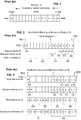
- FIG. 1 illustrates a small 16-byte portion of memory from hexadecimal address 0x1000 to address 0x100F that is loaded into a 128 bit register 21 ( FIG. 2 ) in LE mode and into 128-bit register 28 ( FIG. 3 ) in BE mode.
- each byte from memory is loaded from the first location in memory at address 0x1000 to the LSB of the illustrated registers 21, 28.
- byte "0" from memory address 0x1000 is loaded to the LSB location of registers 21, 28.
- Byte "1" from memory address 0x1001 is loaded next to it and so on until the last byte "15" is loaded in the MSB location of the registers 21, 28.
- FIG. 2 shows arrangements 25-27 corresponding to LE mode for data elements that include byte data elements 25 (i[0]-i[15]), half-word data elements 26 (i[0]-i[8]), and word data elements 27 (i[0]-i[3]).
- FIG. 3 shows arrangements 30-33 for data elements that include byte data elements 30 (i[0]-i[15]), half-word data elements 31 (i[0]-i[8]), word data elements 32 (i[0]-i[3]), and double word sized data elements 33 (i[0]-i[2]), respectively, for BE mode.
- BE mode the register needs to be loaded based on the element size of the operation that is intended to be performed.
- a processor architecture that supports BE operation would need to be able to map the contents of memory into registers, as in the example.
- Such an architecture needs to have load instructions that specify the data element size intended to be loaded when intending to perform some kind of operation on subsets of the data in the register, such as, but not exclusively, an SIMD operation. For example, a load instruction that is 128 bits in length and contains data elements of word size, each 32 bits, so that this example instruction contains four 32-bit word data elements.
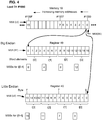
- FIG. 4 illustrates the concept of single load/store instructions to load/write multiple instruction operands with single load/store command.
- the word data element of the first word i[0] contains four bytes that have been reordered into the order of byte 3 in the MSB location on the far left side, with byte 2 next to byte 3, with byte 1 next to byte 2 and with byte 0 in the LSB position.
- the word data elements 32 are reordered to have their MSB on the left side and their LSB on the right side.
- word data elements 32 do not have the same sequential ordering of bytes at they were found in memory 10; therefore, these bytes need to be aligned (e.g., swizzled) into proper position before being loaded into the register 28.
- SIMD instructions such as Arithmetic Logic Unit (ALU) instructions
- ALU Arithmetic Logic Unit
- a processor architecture does not need to include different instructions for big and little endian operation for register/register (e.g., ALU) operations. For example, there is no need for a different multiply instruction for a word-sized multiplication for big and little endian operations, nor is there a need for a signal input into a pipeline that indicates such operating mode.
- register/register e.g., ALU
- FIG. 4 depicts one aspect of the current invention in which a single load instruction can be used for loading a 40 register with data of any data element size.
- a load/store unit that executes the load instruction is sensitized to endian mode.
- the LSU merely takes the byte at the starting address byte 0 for the load (here effective address #1000) and either loads it as shown for BE or for LE mode.
- FIG. 4 shows that in BE mode, the starting address byte 0 is found at the far left of the register 40, and for LE mode, the starting address byte 0 is found at the far right.
- the location of the elements within the register 40 differ between BE and LE mode.
- FIG. 4 also depicts the most significant bytes of the word data element i[0-4] for each of BE and LE mode. As would be appreciated in the example of FIG. 4 , the MSBs for both BE and LE are at the left side of each of these word data elements i[0]. However, in LE mode, the MSB of word data element i[0] is byte 3 and in BE mode, the MSB of i[0] is byte 0.
- the data arranging that occurs in embodiments according to FIG. 4 is simpler than the data arranging that would be required in a standard architecture in which the same data elements of the array are located in the same positions in the register and with the same ordering for both BE and LE modes. Again, this is because prior standard architectures initially loaded elements in the same locations for both BE and LE modes as illustrated in FIGs. 2 and 3 .
- BE mode byte reordering was required for data elements of size half-word and greater to be sure the MSB was at the left side of each data element.
- the single load instruction illustrated in FIG. 4 loads the register 40 in BE mode, it loads it with the MSB, byte 0, at the left end of the register 40 and so on with the LSB, byte 15, loaded at the right end. This ensures that no byte reordering is needed to ensure the MSB is at the left end of the register 40 and is also at the left end of each data element that is a half-word or larger.
- FIG. 5 depicts a memory 300, a memory interface 302 and a register 304, with the memory interface containing lane arranging logic 306.
- the memory interface 302 loads data elements of any size in response to a single load instruction as shown in the example of FIG. 4 and stores data to memory in response to a single store instruction.
- Such a memory interface 302 would perform an inverse operation in order to perform a store, in dependence on the endian mode, but independent of an element size of the data in the register 304. For example, when performing an LE mode load, the memory interface 302 would fetch bytes 15 to 0 from memory 10 ( FIG.
- the lane arranging logic 306 does not need to reorder/change lanes of the bytes.
- the memory interface 302 would again fetch bytes 15 to 0 from the memory 10 ( FIG. 4 ) and store them in register 304 with MSB (BE) byte 0 at the far left side and byte 15 at the far right side of register 321. This is because the MSB in byte ordering for BE is byte 0 and the LSB is byte 15, requiring the lane arranging logic 306 to reorder the bytes loaded from memory 10 before they are placed in the register 304.
- logic and/or processor includes but is not limited to hardware, firmware, software and/or combinations of each to perform a function(s) or an action(s), and/or to cause a function or action from another logic, method, and/or system.
- logic and/or processor may include a software-controlled microprocessor, discrete logic, an application specific integrated circuit (ASIC), a programmed logic device, a memory device containing instructions or the like.
- ASIC application specific integrated circuit
- Logic and/or processor may include one or more gates, combinations of gates, or other circuit components.
- Logic and/or a processor may also be fully embodied as software.
- multiple logics and/or processors are described, it may be possible to incorporate the multiple logics and/or processors into one physical logic (or processor). Similarly, where a single logic and/or processor is described, it may be possible to distribute that single logic and/or processor between multiple physical logics and/or processors.
- FIG. 6 depicts an example of arithmetic unit 320 that is part of an instruction execution pipeline.
- the arithmetic unit 320 may be an unmodified existing arithmetic unit that does not need to account for an endian mode which it is operating. This is because input reordering logic 315 and optional output reordering logic 325, when necessary, have the capability to rearrange input and output data elements so that they are properly aligned. As discussed below, multiplexers and other data bus steering logic may reorder input bytes and output bytes based on what BL/LE mode 310 the arithmetic unit(s) 320 is operating on in accordance with one or more instruction configuration inputs 323.
- instruction configuration input(s) 323 may describe an ordering of data elements such as word, double word, etc. which may depend on more than the LE/BE mode 310 and may be specified by an instruction being executed.
- FIGS. 8 and 9 illustrate some example orderings of inputs bytes for various example SIMD multiply instructions.
- the output reordering logic 325 reorders data elements or other outputs so that output data is stored in the correct locations of the destination register.
- FIG. 7 illustrates an example method 400 of arranging source register bytes and resulting destination register bytes based on an endian mode in which the method 400 is operating.
- This example method 400 is illustrated with reference to flow a diagram. While for purposes of simplicity of explanation, the illustrated methodology are shown and described as a series of blocks, it is to be appreciated that the methodology is not limited by the order of the blocks, as some blocks can occur in different orders and/or concurrently with other blocks from that shown and described. Moreover, less than all the illustrated blocks may be required to implement the example methodology. Blocks may be combined or separated into multiple components. Furthermore, additional and/or alternative methodologies can employ additional, not illustrated, blocks.
- the example method 400 begins at 403 by decoding a prior fetched instruction to determine its source and destination operands and what type of instruction is to be executed.
- the decoded instruction is routed to a reservation station at 405.
- a reservation station provides a way for an out-of-order pipeline to write speculative intermediate results of the execution of an instruction before fully retiring an instruction in programming order.
- LSU load store unit
- a load is performed in the load store unit (LSU) pipeline, at 410, that loads one or more registers from memory. This load is performed based, at least in part on the endian mode (BE or LE).
- the load is invariant as to whether a register is loaded with SIMD or the data element size of the SIMD data. For example, based on endian mode, the register may be loaded as illustrated in FIG. 4 and a single load instruction may be used to load a register with any data element size.
- the instruction After being associated with an entry in the reservation station, the instruction is scheduled for execution at 415.
- source operands associated with the instruction are obtained from corresponding registers at 423.
- the source operand bytes/bits are aligned at 425 based, at least in part, on the endian mode as well as the data element size (byte, half-word, word, double-word) of the SIMD operation of the instruction.
- the instruction is executed/performed at 428 and when required the resulting byte/bits are aligned based, at least in part, on the ending mode at 430.
- the destination register(s) and, if needed, the reservation station are updated with the execution results at 432.
- the method 400 at 434 sends data to be stored to the LSU pipeline so that the results are stored to memory based on endian mode but invariant to whether register stores SIMD data, and invariant to the size of SIMD data being stored.
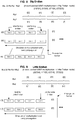
- FIG. 8 depicts an example of a quad-word multiply in BE mode.
- source register Rs1 is being multiplied with source register Rs2 in BE mode.
- FIG. 9 depicts a similar multiplication in LE mode.
- data element word i[0] is being multiplied with i[4], i[1] with [5] and so on.
- words of a SIMD instruction are being multiplied but in other examples, bytes, half-words, double-words or other data element sizes of SIMD data may be similarly multiplied.
- FIGs. 8 and 9 illustrate that because these data element words are located in respectively different locations, different pairs of data elements may be multiplied together at different times if fewer than four ALUs are available.
- the four multiplications may be performed in parallel.
- words i[0] and i[4] are first multiplied together, then words i[1] and i[5] are multiplied together, next i[2] and i[6], and then i[3] and i[7] are multiplied together as the SIMD instruction flows through the ALU pipeline.
- words i[3] and i[7] are first multiplied together, then words i[2] and i[6] are multiplied together, next i[1] and i[5], and then i[0] and i[4] are multiplied together.
- the ALU/execution unit also requires an input for the word/element size in order to determine when to determine how to align some input data and some output data.
- the propagation barriers between pipeline stages for the multiplication of words terminate the carry propagation after two words have been multiplied.
- the bytes have the same ordering so that there, in these two examples, is no need to do a byte-by-byte remapping.
- an execution unit when an execution unit performs a search of the register 40 of FIG. 4 for a particular data element value, it starts at the element at the left end of the register and proceeds to the element at the right end in BE mode and it starts at the element at the right end of the register and proceeds to the element at the left end in LE mode.
- a search instruction starts at the least significant element of a register and searches element-by-element for a particular value until it reaches the most significant element. In LE mode, the first element is at the right end of the register and in BE mode, the first element is at the left end of the register. If the search value is not found in the register, the search instruction may return a signal that indicates no match was found.
- FIGs. 10-13 depict a different example of a single load instruction that can be used to load a register with any size of data elements.
- this load instruction is similar to a classical load instruction.
- the load instruction of FIGs. 10-13 does not account for possible sizes of data elements at the time of load.
- a load instruction Load D1 #1000
- the same relative arrangement of the array members is maintained between both BE and LE modes (e.g., i[0] would be in the same location, regardless whether the load was in BE or LE mode).
- i[0] would be in the same location, regardless whether the load was in BE or LE mode.
- register D1 is loaded with word data element i[0] containing bytes 3-0, word data element i[1] containing bytes 7-4, word data element i[2] containing bytes 11-8, and word data element i[3] containing bytes 15-12.
- word data element i[0] containing bytes 3-0 word data element i[1] containing bytes 7-4
- word data element i[2] containing bytes 11-8
- word data element i[3] containing bytes 15-12.
- FIGs. 11 and 12 illustrate a 4-word packed SMID multiplication of source register one (Rs1) 205 and source register two (Rs2) 210 in BE mode.
- Rs1 205 has been loaded with data element words (e.g., elements) i[3], i[2], i[1], i[0] and Rs1 205 has been loaded with data element words i[7], i[6], i[5], i[4].
- the corresponding byte positions of Rs2 210 are illustrated in FIG. 12 .
- This instruction multiplies word i[3] with word i[7], word i[2] with word i[6], word i[1] with word i[5], and word i[0] with word i[4].
- the byes of each word are properly aligned.
- the bytes of each word must be realigned as illustrated in FIG. 13 for words i[0] and i[4].
- This realignment, or swizzeling may be performed with lane arranging/alignment logic similar to lane arranging logic 306 discussed above with reference to FIG. 5 or with logic similar to the input reordering logic 315 of FIG. 6 .
- this alignment logic may be implemented similarly to alignment logic implemented in graphics processing units (GPUs).
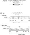
- FIG. 14 depicts an example of a search instruction that identifies a first appearance of an element (e.g., byte) value while searching elements (e.g., bytes) having smaller address values to elements having larger address values.
- these search instructions are executed by an execution unit that is sensitized according to endian mode.
- the ordering logic is reversed between BE and LE mode, as shown in FIG. 14 .
- BE mode a search of a register starts at the left side of the register and proceeds element-to-element toward the rights side of the register until an element is found in the register that matches the search value or the entire register has been searched.
- the execution unit will generate an indication there was no matching element in that register.
- the search is reversed and the search of the register begins at the right side and proceeds element-to-element toward the left side of the register until an element is found in the register that matches the search value or the entire register has been searched.
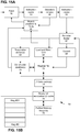
- FIGs. 15A and 15B present an example block diagram of a processor 50 that can implement the disclosure.
- the load store unit (LSU) 66 can execute load and store instructions in accordance with the disclosure to perform the mapping described between memory and register for each mode.
- Instruction execution pipelines 70 (can be in or out of order) are provided an endian mode signal that indicates operating mode.
- the endian mode signal also can be a register bit that is set to indicate the endian mode.
- the fetch logic 52 pre-fetches software instructions from memory that the processor 50 will execute. These pre-fetched instructions are placed in an instruction cache 54. These instructions are later removed from the instruction cache 54 by the decode and rename logic 56 and decoded into instructions that the processor can process. These instructions are also renamed and placed in the instruction queue 58.
- the decoder and rename logic 56 also provides information associated with branch instructions to the branch predictor and Instruction Translation Lookaside Buffers (ITLBs) 60.
- the branch predictor and ILTBs 60 predict branches and provides this branch prediction information to the fetch logic 52 so instructions of predicted branches are fetched.
- a re-order buffer 62 stores results of speculatively completed instructions that may not be ready to retire in programing order.
- the re-order buffer 62 may also be used to unroll miss-predicted branches.
- the reservation station(s) 68 provides a location for instructions to write their results to without requiring a register to become available.
- the reservation station(s) 68 also provide for register renaming and dynamic instruction rescheduling.
- the commit unit 60 determines when instruction data values are ready to be committed/loaded into one or more registers in the register file 72.
- the load and store unit 66 monitors load and store instructions to and from memory to be sure this memory data follows sequential program order, even though the processor 50 is speculatively executing instructions out of order. For example, the load and store unit will not allow a load to load data from a memory location that a pending older store instruction has not yet written.
- FIG. 15B illustrates an example register file with 32 registers Reg #0 through Reg #31.
- data results from the register file 72 may eventually be written into one or more level one (L1) data cache(s) 74 and an N-way set associative level two (L2) cache 76 before reaching a memory hierarchy 78.
- L1 level one
- L2 N-way set associative level two
- both load and store instructions require significantly more opcode space to express than register-to-register instructions.
- a load with a source, destination, and a 16 bit offset would typically require five bits to identify 1 of 32 source registers as well as five bits to identify 1 of 32 destination registers and 16 address offset bits for a total of 26 bits of opcode space leaving the last six bits of the 32 bit opcode free to identify an instruction as a load.
- a register-to-register instruction without an offset would need 15 bits to specify three registers leaving more opcode bits available to identify the type of load instruction.
- an architecture may have 32 registers with each register identified with five bits, and may have an opcode of six bits. Such an architecture would use only 21 bits for encoding such a register-to-register operation. While a RISC architecture may still store that instruction in 32 bits, using only 21 bits of the space allows many more instructions to be encoded. Alternatively, more registers can be addressed, or some combination thereof. Further, the lane arranging logic 306 in the memory interface 302 ( FIG. 5 ) can be simpler than in prior systems, in that it does not need to perform a byte-specific reordering.
- processing units may need to be sensitized to endian mode, there typically already would be sufficient lane reordering logic to support varied logical or arithmetic operations on specified lanes of different sizes. This logic can be supplemented to take endian mode into account.
- 'processor' further includes any of a variety of machine structures that can process or handle data, including, for example, a Digital Signal Processor, fixed function circuitry, input/output (I/O), or even functional units within processor. Still further, 'processor' includes virtualized execution resources, such that one set of physical execution resources can be abstracted as multiple physical processors.
- An operative distinction is whether support for prefetching data into relatively local storage, from relatively remote storage is provided, and subsidiary distinction that may call for implementing the disclosure are the capability of reordering of demand requests, from out of order processing, multithreading, or both.
- Modern general purpose processors regularly require in excess of two billion transistors to be implemented, while graphics processing units may have in excess of five billion transistors. Such transistor counts are likely to increase. Such processors have used these transistors to implement increasing complex operation reordering, prediction, more parallelism, larger memories (including more and bigger caches) and so on. As such, it becomes necessary to be able to describe or discuss technical subject matter concerning such processors, whether general purpose or application specific, at a level of detail appropriate to the technology being addressed. In general, a hierarchy of concepts is applied to allow those of ordinary skill to focus on details of the matter being addressed.
- high level features such as what instructions a processor supports conveys architectural-level detail.
- high-level technology such as a programming model
- microarchitecture detail describes high level detail concerning an implementation of architecture (even as the same microarchitecture may be able to execute different ISAs).
- microarchitecture detail typically describes different functional units and their interrelationship, such as how and when data moves among these different functional units.
- referencing these units by their functionality is also an appropriate level of abstraction, rather than addressing implementations of these functional units, since each of these functional units may themselves comprise hundreds of thousands or millions of gates.
- circuitry does not imply a single electrically connected set of circuits. Circuitry may be fixed function, configurable, or programmable. In general, circuitry implementing a functional unit is more likely to be configurable, or may be more configurable, than circuitry implementing a specific portion of a functional unit. For example, an Arithmetic Logic Unit (ALU) of a processor may reuse the same portion of circuitry differently when performing different arithmetic or logic operations. As such, that portion of circuitry is effectively circuitry or part of circuitry for each different operation, when configured to perform or otherwise interconnected to perform each different operation. Such configuration may come from or be based on instructions, or microcode, for example.
- ALU Arithmetic Logic Unit
- the term "unit” refers, in some implementations, to a class or group of circuitry that implements the functions or functions attributed to that unit. Such circuitry may implement additional functions, and so identification of circuitry performing one function does not mean that the same circuitry, or a portion thereof, cannot also perform other functions. In some circumstances, the functional unit may be identified, and then functional description of circuitry that performs a certain feature differently, or implements a new feature, may be described. For example, a "decode unit” refers to circuitry implementing decoding of processor instructions.
- decode unit and hence circuitry implementing such decode unit, supports decoding of specified instruction types.
- Decoding of instructions differs across different architectures and microarchitectures, and the term makes no exclusion thereof, except for the explicit requirements of the claims.
- different microarchitectures may implement instruction decoding and instruction scheduling somewhat differently, in accordance with design goals of that implementation.
- structures have taken their names from the functions that they perform.
- a "decoder" of program instructions that behaves in a prescribed manner, describes structure supports that behavior.
- the structure may have permanent physical differences or adaptations from decoders that do not support such behavior.
- such structure also may be produced by a temporary adaptation or configuration, such as one caused under program control, microcode, or other source of configuration.
- circuitry may be synchronous or asynchronous with respect to a clock.
- Circuitry may be designed to be static or be dynamic.
- Different circuit design philosophies may be used to implement different functional units or parts thereof. Absent some context-specific basis, "circuitry" encompasses all such design approaches.
- circuitry or functional units described herein may be most frequently implemented by electrical circuitry, and more particularly, by circuitry that primarily relies on a transistor implemented in a semiconductor as a primary switch element, this term is to be understood in relation to the technology being disclosed.
- different physical processes may be used in circuitry implementing aspects of the disclosure, such as optical, nanotubes, micro-electrical mechanical elements, quantum switches or memory storage, magneto resistive logic elements, and so on.
- a choice of technology used to construct circuitry or functional units according to the technology may change over time, this choice is an implementation decision to be made in accordance with the then-current state of technology.
- Functional modules may be composed of circuitry, where such circuitry may be a fixed function, configurable under program control or under other configuration information, or some combination thereof. Functional modules themselves thus may be described by the functions that they perform, to helpfully abstract how some of the constituent portions of such functions may be implemented.
- circuitry and functional modules may be described partially in functional terms, and partially in structural terms. In some situations, the structural portion of such a description may be described in terms of a configuration applied to circuitry or to functional modules, or both.
- a means for performing implementations of software processes described herein includes machine-executable code used to configure a machine to perform such process.
- Some aspects of the disclosure pertain to processes carried out by limited configurability or fixed function circuits and in such situations, means for performing such processes include one or more of special purpose and limited-programmability hardware.
- Such hardware can be controlled or invoked by software executing on a general purpose computer.
- Implementations of the disclosure may be provided for use in embedded systems, such as televisions, appliances, vehicles, or personal computers, desktop computers, laptop computers, message processors, hand-held devices, multi-processor systems, microprocessor-based or programmable consumer electronics, game consoles, network PCs, minicomputers, mainframe computers, mobile telephones, PDAs, tablets and the like.
- embedded systems such as televisions, appliances, vehicles, or personal computers, desktop computers, laptop computers, message processors, hand-held devices, multi-processor systems, microprocessor-based or programmable consumer electronics, game consoles, network PCs, minicomputers, mainframe computers, mobile telephones, PDAs, tablets and the like.
- implementations may also be embodied in software (e.g., computer readable code, program code, instructions and/or data disposed in any form, such as source, object or machine language) disposed, for example, in a computer usable (e.g., readable) medium configured to store the software.
- software e.g., computer readable code, program code, instructions and/or data disposed in any form, such as source, object or machine language
- a computer usable (e.g., readable) medium configured to store the software.
- Such software can enable, for example, the function, fabrication, modeling, simulation, description, and/or testing of the apparatus and methods described herein.
- Embodiments can be disposed in computer usable medium including non-transitory memories such as memories using semiconductor, magnetic disk, optical disk, ferrous, resistive memory, and so on.
- implementations of disclosed apparatuses and methods may be implemented in a semiconductor intellectual property core, such as a microprocessor core, or a portion thereof, embodied in a Hardware Description Language (HDL), that can be used to produce a specific integrated circuit implementation.
- a computer readable medium may embody or store such description language data, and thus constitute an article of manufacture.
- a non-transitory machine readable medium is an example of computer-readable media. Examples of other embodiments include computer readable media storing Register Transfer Language (RTL) description that may be adapted for use in a specific architecture or microarchitecture implementation.
- RTL Register Transfer Language
- the apparatus and methods described herein may be embodied as a combination of hardware and software that configures or programs hardware.
Landscapes
- Engineering & Computer Science (AREA)
- Theoretical Computer Science (AREA)
- Software Systems (AREA)
- Physics & Mathematics (AREA)
- General Physics & Mathematics (AREA)
- General Engineering & Computer Science (AREA)
- Mathematical Physics (AREA)
- Mathematical Analysis (AREA)
- Mathematical Optimization (AREA)
- Pure & Applied Mathematics (AREA)
- Computational Mathematics (AREA)
- Computer Hardware Design (AREA)
- Computing Systems (AREA)
- Executing Machine-Instructions (AREA)
Applications Claiming Priority (1)
| Application Number | Priority Date | Filing Date | Title |
|---|---|---|---|
| US14/930,740 US20170123792A1 (en) | 2015-11-03 | 2015-11-03 | Processors Supporting Endian Agnostic SIMD Instructions and Methods |
Publications (2)
| Publication Number | Publication Date |
|---|---|
| EP3166014A1 true EP3166014A1 (de) | 2017-05-10 |
| EP3166014B1 EP3166014B1 (de) | 2020-04-01 |
Family
ID=57389185
Family Applications (1)
| Application Number | Title | Priority Date | Filing Date |
|---|---|---|---|
| EP16196647.8A Active EP3166014B1 (de) | 2015-11-03 | 2016-10-31 | Prozessoren zur unterstützung von endian-agnostischer simd-anweisungen und verfahren |
Country Status (4)
| Country | Link |
|---|---|
| US (1) | US20170123792A1 (de) |
| EP (1) | EP3166014B1 (de) |
| CN (1) | CN107038020A (de) |
| GB (1) | GB2545081A (de) |
Cited By (1)
| Publication number | Priority date | Publication date | Assignee | Title |
|---|---|---|---|---|
| WO2020169365A1 (en) * | 2019-02-19 | 2020-08-27 | International Business Machines Corporation | Load/store bytes reversed elements instructions |
Families Citing this family (9)
| Publication number | Priority date | Publication date | Assignee | Title |
|---|---|---|---|---|
| US10671387B2 (en) | 2014-06-10 | 2020-06-02 | International Business Machines Corporation | Vector memory access instructions for big-endian element ordered and little-endian element ordered computer code and data |
| US10691456B2 (en) * | 2015-11-13 | 2020-06-23 | International Business Machines Corporation | Vector store instruction having instruction-specified byte count to be stored supporting big and little endian processing |
| US10691453B2 (en) | 2015-11-13 | 2020-06-23 | International Business Machines Corporation | Vector load with instruction-specified byte count less than a vector size for big and little endian processing |
| US10101997B2 (en) | 2016-03-14 | 2018-10-16 | International Business Machines Corporation | Independent vector element order and memory byte order controls |
| US10459700B2 (en) * | 2016-03-14 | 2019-10-29 | International Business Machines Corporation | Independent vector element order and memory byte order controls |
| US20200264877A1 (en) * | 2019-02-19 | 2020-08-20 | International Business Machines Corporation | Load/store elements reversed instructions |
| GB2582785A (en) * | 2019-04-02 | 2020-10-07 | Graphcore Ltd | Compiling a program from a graph |
| US11886377B2 (en) | 2019-09-10 | 2024-01-30 | Cornami, Inc. | Reconfigurable arithmetic engine circuit |
| CN112835842B (zh) * | 2021-03-05 | 2024-04-30 | 深圳市汇顶科技股份有限公司 | 端序处理方法、电路、芯片以及电子终端 |
Citations (6)
| Publication number | Priority date | Publication date | Assignee | Title |
|---|---|---|---|---|
| US20040030856A1 (en) * | 2002-08-07 | 2004-02-12 | Qureshi Shiraz A. | System and method for operating in endian independent mode |
| US6728874B1 (en) * | 2000-10-10 | 2004-04-27 | Koninklijke Philips Electronics N.V. | System and method for processing vectorized data |
| US20050125476A1 (en) * | 2003-12-09 | 2005-06-09 | Arm Limited | Data processing apparatus and method for performing arithmetic operations in SIMD data processing |
| WO2007103195A2 (en) * | 2006-03-06 | 2007-09-13 | Analog Devices. Inc. | Improved permutable address processor and method |
| US20110072170A1 (en) * | 2009-09-21 | 2011-03-24 | Brian King Flachs | Systems and Methods for Transferring Data to Maintain Preferred Slot Positions in a Bi-endian Processor |
| US20150248290A1 (en) * | 2014-02-28 | 2015-09-03 | International Business Machines Corporation | Virtualization in a bi-endian-mode processor architecture |
Family Cites Families (15)
| Publication number | Priority date | Publication date | Assignee | Title |
|---|---|---|---|---|
| DE3687124T2 (de) * | 1986-02-06 | 1993-03-18 | Mips Computer Systems Inc | Funktionseinheit fuer rechner. |
| US5687337A (en) * | 1995-02-24 | 1997-11-11 | International Business Machines Corporation | Mixed-endian computer system |
| US7047383B2 (en) * | 2002-07-11 | 2006-05-16 | Intel Corporation | Byte swap operation for a 64 bit operand |
| GB2409067B (en) * | 2003-12-09 | 2006-12-13 | Advanced Risc Mach Ltd | Endianess compensation within a SIMD data processing system |
| US7454585B2 (en) * | 2005-12-22 | 2008-11-18 | International Business Machines Corporation | Efficient and flexible memory copy operation |
| WO2009105332A1 (en) * | 2008-02-18 | 2009-08-27 | Sandbridge Technologies, Inc. | Method to accelerate null-terminated string operations |
| US20110082999A1 (en) * | 2009-10-07 | 2011-04-07 | Andes Technology Corporation | Data processing engine with integrated data endianness control mechanism |
| JP5622429B2 (ja) * | 2010-04-20 | 2014-11-12 | ルネサスエレクトロニクス株式会社 | マイクロコンピュータ |
| US9672036B2 (en) * | 2011-09-26 | 2017-06-06 | Intel Corporation | Instruction and logic to provide vector loads with strides and masking functionality |
| US9336072B2 (en) * | 2014-02-07 | 2016-05-10 | Ralph Moore | Event group extensions, systems, and methods |
| US20150227366A1 (en) * | 2014-02-12 | 2015-08-13 | Imagination Technologies Limited | Processor with granular add immediates capability & methods |
| US9507595B2 (en) * | 2014-02-28 | 2016-11-29 | International Business Machines Corporation | Execution of multi-byte memory access instruction specifying endian mode that overrides current global endian mode |
| US9619214B2 (en) * | 2014-08-13 | 2017-04-11 | International Business Machines Corporation | Compiler optimizations for vector instructions |
| US9588746B2 (en) * | 2014-12-19 | 2017-03-07 | International Business Machines Corporation | Compiler method for generating instructions for vector operations on a multi-endian processor |
| US9569190B1 (en) * | 2015-08-04 | 2017-02-14 | International Business Machines Corporation | Compiling source code to reduce run-time execution of vector element reverse operations |
-
2015
- 2015-11-03 US US14/930,740 patent/US20170123792A1/en not_active Abandoned
-
2016
- 2016-10-31 EP EP16196647.8A patent/EP3166014B1/de active Active
- 2016-10-31 GB GB1618384.0A patent/GB2545081A/en not_active Withdrawn
- 2016-11-03 CN CN201610959252.6A patent/CN107038020A/zh active Pending
Patent Citations (6)
| Publication number | Priority date | Publication date | Assignee | Title |
|---|---|---|---|---|
| US6728874B1 (en) * | 2000-10-10 | 2004-04-27 | Koninklijke Philips Electronics N.V. | System and method for processing vectorized data |
| US20040030856A1 (en) * | 2002-08-07 | 2004-02-12 | Qureshi Shiraz A. | System and method for operating in endian independent mode |
| US20050125476A1 (en) * | 2003-12-09 | 2005-06-09 | Arm Limited | Data processing apparatus and method for performing arithmetic operations in SIMD data processing |
| WO2007103195A2 (en) * | 2006-03-06 | 2007-09-13 | Analog Devices. Inc. | Improved permutable address processor and method |
| US20110072170A1 (en) * | 2009-09-21 | 2011-03-24 | Brian King Flachs | Systems and Methods for Transferring Data to Maintain Preferred Slot Positions in a Bi-endian Processor |
| US20150248290A1 (en) * | 2014-02-28 | 2015-09-03 | International Business Machines Corporation | Virtualization in a bi-endian-mode processor architecture |
Cited By (1)
| Publication number | Priority date | Publication date | Assignee | Title |
|---|---|---|---|---|
| WO2020169365A1 (en) * | 2019-02-19 | 2020-08-27 | International Business Machines Corporation | Load/store bytes reversed elements instructions |
Also Published As
| Publication number | Publication date |
|---|---|
| US20170123792A1 (en) | 2017-05-04 |
| GB2545081A (en) | 2017-06-07 |
| GB201618384D0 (en) | 2016-12-14 |
| CN107038020A (zh) | 2017-08-11 |
| EP3166014B1 (de) | 2020-04-01 |
Similar Documents
| Publication | Publication Date | Title |
|---|---|---|
| EP3166014B1 (de) | Prozessoren zur unterstützung von endian-agnostischer simd-anweisungen und verfahren | |
| TWI423127B (zh) | 指令處理方法以及其所適用之超純量管線微處理器 | |
| US11379234B2 (en) | Store-to-load forwarding | |
| US9448936B2 (en) | Concurrent store and load operations | |
| CN106648554B (zh) | 用于改善连续的事务性存储器区的吞吐量的系统、方法和装置 | |
| CN204945992U (zh) | 一种处理器 | |
| US8769539B2 (en) | Scheduling scheme for load/store operations | |
| US10747539B1 (en) | Scan-on-fill next fetch target prediction | |
| EP3179375B1 (de) | Prozessor mit programmierbarem prefetcher | |
| US20150227365A1 (en) | Processor Supporting Arithmetic Instructions with Branch on Overflow & Methods | |
| US20150242212A1 (en) | Modeless instruction execution with 64/32-bit addressing | |
| US8880854B2 (en) | Out-of-order execution microprocessor that speculatively executes dependent memory access instructions by predicting no value change by older instructions that load a segment register | |
| CN107885530B (zh) | 提交高速缓存行的方法和指令高速缓存 | |
| JP3678443B2 (ja) | スーパーパイプライン式スーパースカラーマイクロプロセッサ用の書き込みバッファ | |
| JP7156776B2 (ja) | リタイアフェーズ中に部分書込み結果をマージするシステムおよび方法 | |
| HK1214377A1 (zh) | 具有世代重命名的計算機處理器 | |
| US9223577B2 (en) | Processing multi-destination instruction in pipeline by splitting for single destination operations stage and merging for opcode execution operations stage | |
| US10649773B2 (en) | Processors supporting atomic writes to multiword memory locations and methods | |
| CN106170761A (zh) | 用于在二进制转换中横跨多个原子区调度存储指令的方法和装置 | |
| US9626185B2 (en) | IT instruction pre-decode | |
| CN101535947A (zh) | 两次发布的条件移动指令及其应用 | |
| US9959122B2 (en) | Single cycle instruction pipeline scheduling | |
| US11175917B1 (en) | Buffer for replayed loads in parallel with reservation station for rapid rescheduling | |
| US20220137976A1 (en) | Removal of Dependent Instructions from an Execution Pipeline | |
| US7721073B2 (en) | Conditional branch execution in a processor having a data mover engine that associates register addresses with memory addresses |
Legal Events
| Date | Code | Title | Description |
|---|---|---|---|
| PUAI | Public reference made under article 153(3) epc to a published international application that has entered the european phase |
Free format text: ORIGINAL CODE: 0009012 |
|
| STAA | Information on the status of an ep patent application or granted ep patent |
Free format text: STATUS: THE APPLICATION HAS BEEN PUBLISHED |
|
| AK | Designated contracting states |
Kind code of ref document: A1 Designated state(s): AL AT BE BG CH CY CZ DE DK EE ES FI FR GB GR HR HU IE IS IT LI LT LU LV MC MK MT NL NO PL PT RO RS SE SI SK SM TR |
|
| AX | Request for extension of the european patent |
Extension state: BA ME |
|
| STAA | Information on the status of an ep patent application or granted ep patent |
Free format text: STATUS: REQUEST FOR EXAMINATION WAS MADE |
|
| 17P | Request for examination filed |
Effective date: 20171110 |
|
| RBV | Designated contracting states (corrected) |
Designated state(s): AL AT BE BG CH CY CZ DE DK EE ES FI FR GB GR HR HU IE IS IT LI LT LU LV MC MK MT NL NO PL PT RO RS SE SI SK SM TR |
|
| STAA | Information on the status of an ep patent application or granted ep patent |
Free format text: STATUS: EXAMINATION IS IN PROGRESS |
|
| 17Q | First examination report despatched |
Effective date: 20181029 |
|
| GRAP | Despatch of communication of intention to grant a patent |
Free format text: ORIGINAL CODE: EPIDOSNIGR1 |
|
| STAA | Information on the status of an ep patent application or granted ep patent |
Free format text: STATUS: GRANT OF PATENT IS INTENDED |
|
| INTG | Intention to grant announced |
Effective date: 20191014 |
|
| RIN1 | Information on inventor provided before grant (corrected) |
Inventor name: RANGANATHAN, SUDHAKAR Inventor name: ROZARIO, RANJIT J. |
|
| RAP1 | Party data changed (applicant data changed or rights of an application transferred) |
Owner name: MIPS TECH, LLC |
|
| GRAS | Grant fee paid |
Free format text: ORIGINAL CODE: EPIDOSNIGR3 |
|
| GRAA | (expected) grant |
Free format text: ORIGINAL CODE: 0009210 |
|
| STAA | Information on the status of an ep patent application or granted ep patent |
Free format text: STATUS: THE PATENT HAS BEEN GRANTED |
|
| AK | Designated contracting states |
Kind code of ref document: B1 Designated state(s): AL AT BE BG CH CY CZ DE DK EE ES FI FR GB GR HR HU IE IS IT LI LT LU LV MC MK MT NL NO PL PT RO RS SE SI SK SM TR |
|
| REG | Reference to a national code |
Ref country code: GB Ref legal event code: FG4D |
|
| REG | Reference to a national code |
Ref country code: CH Ref legal event code: EP Ref country code: AT Ref legal event code: REF Ref document number: 1252243 Country of ref document: AT Kind code of ref document: T Effective date: 20200415 |
|
| REG | Reference to a national code |
Ref country code: DE Ref legal event code: R096 Ref document number: 602016032919 Country of ref document: DE |
|
| REG | Reference to a national code |
Ref country code: IE Ref legal event code: FG4D |
|
| PG25 | Lapsed in a contracting state [announced via postgrant information from national office to epo] |
Ref country code: BG Free format text: LAPSE BECAUSE OF FAILURE TO SUBMIT A TRANSLATION OF THE DESCRIPTION OR TO PAY THE FEE WITHIN THE PRESCRIBED TIME-LIMIT Effective date: 20200701 |
|
| REG | Reference to a national code |
Ref country code: NL Ref legal event code: MP Effective date: 20200401 |
|
| REG | Reference to a national code |
Ref country code: LT Ref legal event code: MG4D |
|
| PG25 | Lapsed in a contracting state [announced via postgrant information from national office to epo] |
Ref country code: NL Free format text: LAPSE BECAUSE OF FAILURE TO SUBMIT A TRANSLATION OF THE DESCRIPTION OR TO PAY THE FEE WITHIN THE PRESCRIBED TIME-LIMIT Effective date: 20200401 Ref country code: GR Free format text: LAPSE BECAUSE OF FAILURE TO SUBMIT A TRANSLATION OF THE DESCRIPTION OR TO PAY THE FEE WITHIN THE PRESCRIBED TIME-LIMIT Effective date: 20200702 Ref country code: NO Free format text: LAPSE BECAUSE OF FAILURE TO SUBMIT A TRANSLATION OF THE DESCRIPTION OR TO PAY THE FEE WITHIN THE PRESCRIBED TIME-LIMIT Effective date: 20200701 Ref country code: IS Free format text: LAPSE BECAUSE OF FAILURE TO SUBMIT A TRANSLATION OF THE DESCRIPTION OR TO PAY THE FEE WITHIN THE PRESCRIBED TIME-LIMIT Effective date: 20200801 Ref country code: SE Free format text: LAPSE BECAUSE OF FAILURE TO SUBMIT A TRANSLATION OF THE DESCRIPTION OR TO PAY THE FEE WITHIN THE PRESCRIBED TIME-LIMIT Effective date: 20200401 Ref country code: FI Free format text: LAPSE BECAUSE OF FAILURE TO SUBMIT A TRANSLATION OF THE DESCRIPTION OR TO PAY THE FEE WITHIN THE PRESCRIBED TIME-LIMIT Effective date: 20200401 Ref country code: PT Free format text: LAPSE BECAUSE OF FAILURE TO SUBMIT A TRANSLATION OF THE DESCRIPTION OR TO PAY THE FEE WITHIN THE PRESCRIBED TIME-LIMIT Effective date: 20200817 Ref country code: LT Free format text: LAPSE BECAUSE OF FAILURE TO SUBMIT A TRANSLATION OF THE DESCRIPTION OR TO PAY THE FEE WITHIN THE PRESCRIBED TIME-LIMIT Effective date: 20200401 Ref country code: CZ Free format text: LAPSE BECAUSE OF FAILURE TO SUBMIT A TRANSLATION OF THE DESCRIPTION OR TO PAY THE FEE WITHIN THE PRESCRIBED TIME-LIMIT Effective date: 20200401 |
|
| REG | Reference to a national code |
Ref country code: AT Ref legal event code: MK05 Ref document number: 1252243 Country of ref document: AT Kind code of ref document: T Effective date: 20200401 |
|
| PG25 | Lapsed in a contracting state [announced via postgrant information from national office to epo] |
Ref country code: HR Free format text: LAPSE BECAUSE OF FAILURE TO SUBMIT A TRANSLATION OF THE DESCRIPTION OR TO PAY THE FEE WITHIN THE PRESCRIBED TIME-LIMIT Effective date: 20200401 Ref country code: RS Free format text: LAPSE BECAUSE OF FAILURE TO SUBMIT A TRANSLATION OF THE DESCRIPTION OR TO PAY THE FEE WITHIN THE PRESCRIBED TIME-LIMIT Effective date: 20200401 Ref country code: LV Free format text: LAPSE BECAUSE OF FAILURE TO SUBMIT A TRANSLATION OF THE DESCRIPTION OR TO PAY THE FEE WITHIN THE PRESCRIBED TIME-LIMIT Effective date: 20200401 |
|
| PG25 | Lapsed in a contracting state [announced via postgrant information from national office to epo] |
Ref country code: AL Free format text: LAPSE BECAUSE OF FAILURE TO SUBMIT A TRANSLATION OF THE DESCRIPTION OR TO PAY THE FEE WITHIN THE PRESCRIBED TIME-LIMIT Effective date: 20200401 |
|
| REG | Reference to a national code |
Ref country code: DE Ref legal event code: R097 Ref document number: 602016032919 Country of ref document: DE |
|
| PG25 | Lapsed in a contracting state [announced via postgrant information from national office to epo] |
Ref country code: RO Free format text: LAPSE BECAUSE OF FAILURE TO SUBMIT A TRANSLATION OF THE DESCRIPTION OR TO PAY THE FEE WITHIN THE PRESCRIBED TIME-LIMIT Effective date: 20200401 Ref country code: IT Free format text: LAPSE BECAUSE OF FAILURE TO SUBMIT A TRANSLATION OF THE DESCRIPTION OR TO PAY THE FEE WITHIN THE PRESCRIBED TIME-LIMIT Effective date: 20200401 Ref country code: DK Free format text: LAPSE BECAUSE OF FAILURE TO SUBMIT A TRANSLATION OF THE DESCRIPTION OR TO PAY THE FEE WITHIN THE PRESCRIBED TIME-LIMIT Effective date: 20200401 Ref country code: AT Free format text: LAPSE BECAUSE OF FAILURE TO SUBMIT A TRANSLATION OF THE DESCRIPTION OR TO PAY THE FEE WITHIN THE PRESCRIBED TIME-LIMIT Effective date: 20200401 Ref country code: EE Free format text: LAPSE BECAUSE OF FAILURE TO SUBMIT A TRANSLATION OF THE DESCRIPTION OR TO PAY THE FEE WITHIN THE PRESCRIBED TIME-LIMIT Effective date: 20200401 Ref country code: SM Free format text: LAPSE BECAUSE OF FAILURE TO SUBMIT A TRANSLATION OF THE DESCRIPTION OR TO PAY THE FEE WITHIN THE PRESCRIBED TIME-LIMIT Effective date: 20200401 Ref country code: ES Free format text: LAPSE BECAUSE OF FAILURE TO SUBMIT A TRANSLATION OF THE DESCRIPTION OR TO PAY THE FEE WITHIN THE PRESCRIBED TIME-LIMIT Effective date: 20200401 |
|
| PLBE | No opposition filed within time limit |
Free format text: ORIGINAL CODE: 0009261 |
|
| STAA | Information on the status of an ep patent application or granted ep patent |
Free format text: STATUS: NO OPPOSITION FILED WITHIN TIME LIMIT |
|
| PG25 | Lapsed in a contracting state [announced via postgrant information from national office to epo] |
Ref country code: SK Free format text: LAPSE BECAUSE OF FAILURE TO SUBMIT A TRANSLATION OF THE DESCRIPTION OR TO PAY THE FEE WITHIN THE PRESCRIBED TIME-LIMIT Effective date: 20200401 Ref country code: PL Free format text: LAPSE BECAUSE OF FAILURE TO SUBMIT A TRANSLATION OF THE DESCRIPTION OR TO PAY THE FEE WITHIN THE PRESCRIBED TIME-LIMIT Effective date: 20200401 |
|
| 26N | No opposition filed |
Effective date: 20210112 |
|
| PG25 | Lapsed in a contracting state [announced via postgrant information from national office to epo] |
Ref country code: SI Free format text: LAPSE BECAUSE OF FAILURE TO SUBMIT A TRANSLATION OF THE DESCRIPTION OR TO PAY THE FEE WITHIN THE PRESCRIBED TIME-LIMIT Effective date: 20200401 |
|
| REG | Reference to a national code |
Ref country code: CH Ref legal event code: PL |
|
| GBPC | Gb: european patent ceased through non-payment of renewal fee |
Effective date: 20201031 |
|
| PG25 | Lapsed in a contracting state [announced via postgrant information from national office to epo] |
Ref country code: LU Free format text: LAPSE BECAUSE OF NON-PAYMENT OF DUE FEES Effective date: 20201031 Ref country code: MC Free format text: LAPSE BECAUSE OF FAILURE TO SUBMIT A TRANSLATION OF THE DESCRIPTION OR TO PAY THE FEE WITHIN THE PRESCRIBED TIME-LIMIT Effective date: 20200401 |
|
| REG | Reference to a national code |
Ref country code: BE Ref legal event code: MM Effective date: 20201031 |
|
| PG25 | Lapsed in a contracting state [announced via postgrant information from national office to epo] |
Ref country code: FR Free format text: LAPSE BECAUSE OF NON-PAYMENT OF DUE FEES Effective date: 20201031 |
|
| PG25 | Lapsed in a contracting state [announced via postgrant information from national office to epo] |
Ref country code: GB Free format text: LAPSE BECAUSE OF NON-PAYMENT OF DUE FEES Effective date: 20201031 Ref country code: LI Free format text: LAPSE BECAUSE OF NON-PAYMENT OF DUE FEES Effective date: 20201031 Ref country code: BE Free format text: LAPSE BECAUSE OF NON-PAYMENT OF DUE FEES Effective date: 20201031 Ref country code: CH Free format text: LAPSE BECAUSE OF NON-PAYMENT OF DUE FEES Effective date: 20201031 |
|
| PG25 | Lapsed in a contracting state [announced via postgrant information from national office to epo] |
Ref country code: IE Free format text: LAPSE BECAUSE OF NON-PAYMENT OF DUE FEES Effective date: 20201031 |
|
| REG | Reference to a national code |
Ref country code: DE Ref legal event code: R082 Ref document number: 602016032919 Country of ref document: DE Representative=s name: GLOBAL IP EUROPE PATENTANWALTSKANZLEI, DE |
|
| PG25 | Lapsed in a contracting state [announced via postgrant information from national office to epo] |
Ref country code: TR Free format text: LAPSE BECAUSE OF FAILURE TO SUBMIT A TRANSLATION OF THE DESCRIPTION OR TO PAY THE FEE WITHIN THE PRESCRIBED TIME-LIMIT Effective date: 20200401 Ref country code: MT Free format text: LAPSE BECAUSE OF FAILURE TO SUBMIT A TRANSLATION OF THE DESCRIPTION OR TO PAY THE FEE WITHIN THE PRESCRIBED TIME-LIMIT Effective date: 20200401 Ref country code: CY Free format text: LAPSE BECAUSE OF FAILURE TO SUBMIT A TRANSLATION OF THE DESCRIPTION OR TO PAY THE FEE WITHIN THE PRESCRIBED TIME-LIMIT Effective date: 20200401 |
|
| PG25 | Lapsed in a contracting state [announced via postgrant information from national office to epo] |
Ref country code: MK Free format text: LAPSE BECAUSE OF FAILURE TO SUBMIT A TRANSLATION OF THE DESCRIPTION OR TO PAY THE FEE WITHIN THE PRESCRIBED TIME-LIMIT Effective date: 20200401 |
|
| P01 | Opt-out of the competence of the unified patent court (upc) registered |
Effective date: 20230329 |
|
| P02 | Opt-out of the competence of the unified patent court (upc) changed |
Effective date: 20230522 |
|
| PGFP | Annual fee paid to national office [announced via postgrant information from national office to epo] |
Ref country code: DE Payment date: 20251020 Year of fee payment: 10 |