EP3165905A1 - Gas concentration measurement device - Google Patents
Gas concentration measurement device Download PDFInfo
- Publication number
- EP3165905A1 EP3165905A1 EP15815028.4A EP15815028A EP3165905A1 EP 3165905 A1 EP3165905 A1 EP 3165905A1 EP 15815028 A EP15815028 A EP 15815028A EP 3165905 A1 EP3165905 A1 EP 3165905A1
- Authority
- EP
- European Patent Office
- Prior art keywords
- wave
- infrared light
- gas concentration
- measurement device
- concentration measurement
- Prior art date
- Legal status (The legal status is an assumption and is not a legal conclusion. Google has not performed a legal analysis and makes no representation as to the accuracy of the status listed.)
- Granted
Links
Images



Classifications
-
- G—PHYSICS
- G01—MEASURING; TESTING
- G01N—INVESTIGATING OR ANALYSING MATERIALS BY DETERMINING THEIR CHEMICAL OR PHYSICAL PROPERTIES
- G01N21/00—Investigating or analysing materials by the use of optical means, i.e. using sub-millimetre waves, infrared, visible or ultraviolet light
- G01N21/17—Systems in which incident light is modified in accordance with the properties of the material investigated
- G01N21/59—Transmissivity
- G01N21/61—Non-dispersive gas analysers
-
- G—PHYSICS
- G01—MEASURING; TESTING
- G01N—INVESTIGATING OR ANALYSING MATERIALS BY DETERMINING THEIR CHEMICAL OR PHYSICAL PROPERTIES
- G01N21/00—Investigating or analysing materials by the use of optical means, i.e. using sub-millimetre waves, infrared, visible or ultraviolet light
- G01N21/17—Systems in which incident light is modified in accordance with the properties of the material investigated
- G01N21/25—Colour; Spectral properties, i.e. comparison of effect of material on the light at two or more different wavelengths or wavelength bands
- G01N21/31—Investigating relative effect of material at wavelengths characteristic of specific elements or molecules, e.g. atomic absorption spectrometry
- G01N21/35—Investigating relative effect of material at wavelengths characteristic of specific elements or molecules, e.g. atomic absorption spectrometry using infrared light
- G01N21/3504—Investigating relative effect of material at wavelengths characteristic of specific elements or molecules, e.g. atomic absorption spectrometry using infrared light for analysing gases, e.g. multi-gas analysis
-
- G—PHYSICS
- G01—MEASURING; TESTING
- G01N—INVESTIGATING OR ANALYSING MATERIALS BY DETERMINING THEIR CHEMICAL OR PHYSICAL PROPERTIES
- G01N33/00—Investigating or analysing materials by specific methods not covered by groups G01N1/00 - G01N31/00
- G01N33/0004—Gaseous mixtures, e.g. polluted air
- G01N33/0009—General constructional details of gas analysers, e.g. portable test equipment
- G01N33/0027—General constructional details of gas analysers, e.g. portable test equipment concerning the detector
- G01N33/0036—General constructional details of gas analysers, e.g. portable test equipment concerning the detector specially adapted to detect a particular component
- G01N33/004—CO or CO2
-
- G—PHYSICS
- G01—MEASURING; TESTING
- G01N—INVESTIGATING OR ANALYSING MATERIALS BY DETERMINING THEIR CHEMICAL OR PHYSICAL PROPERTIES
- G01N2201/00—Features of devices classified in G01N21/00
- G01N2201/06—Illumination; Optics
- G01N2201/068—Optics, miscellaneous
-
- G—PHYSICS
- G01—MEASURING; TESTING
- G01N—INVESTIGATING OR ANALYSING MATERIALS BY DETERMINING THEIR CHEMICAL OR PHYSICAL PROPERTIES
- G01N2201/00—Features of devices classified in G01N21/00
- G01N2201/08—Optical fibres; light guides
Definitions
- the present invention relates to an infrared-light-absorption gas concentration measurement device.
- infrared-light-absorption gas concentration measurement devices are used to analyze sample gas by utilizing the fact that the sample gas absorbs infrared light in a specific wavelength range.
- Patent Document 1 discloses an infrared-light-absorption gas concentration measurement device.
- an anti-reflection film is applied to inner walls of an analysis chamber (sample cell) that defines a flow channel for the sample gas. Accordingly, the risk that the infrared light will be incident on a band pass filter, which is provided on a surface of a detector, at an angle greater than a predetermined angle is reduced.
- Patent Document 1 International Publication No. 01/27596
- the anti-reflection film disclosed in Patent Document 1 needs to be made of a material having a reflectance close to zero. Thus, the material of the anti-reflection film is limited. If an inexpensive material having a reflectance that is not close to zero is used, the infrared light is reflected by the anti-reflection film and is incident on the band pass filter at an angle greater than the predetermined angle. In such a case, the transmission band of the band pass filter is shifted and the measurement accuracy decreases.
- the present invention has been made in light of the above-described problem, and an object of the present invention is to provide a gas concentration measurement device capable of increasing the measurement accuracy.
- a gas concentration measurement device includes a light source that emits infrared light; a detector that detects the infrared light from the light source through a band pass filter; and a waveguide member including a wave-guiding portion having a tubular inner peripheral surface, an entrance portion that is formed at one side of the wave-guiding portion and through which the infrared light from the light source is introduced, and an exit portion that is formed at the other side of the wave-guiding portion and guides the infrared light that has passed through the wave-guiding portion toward the detector.
- a portion or entirety of the inner peripheral surface of the wave-guiding portion includes a tapered region having a cross section that decreases along a direction from the entrance portion to the exit portion.
- the waveguide member reflects the infrared light that has entered the wave-guiding portion through the entrance portion in the tapered region, so that energy of the infrared light that is obliquely incident on the band pass filter is reduced.
- the tapered region of the inner peripheral surface of the wave-guiding portion includes a truncated conical or pyramidal portion having a perimeter that decreases along a direction from the entrance portion to the exit portion.
- an opening area of the entrance portion is greater than an opening area of the exit portion.
- the tapered region of the inner peripheral surface of the wave-guiding portion includes a first curved portion having a perimeter that decreases along a direction from the entrance portion to the exit portion.
- a length of the first curved portion in an axial direction of the wave-guiding portion is greater than or equal to half a length of the wave-guiding portion in the axial direction of the wave-guiding portion.
- the inner peripheral surface of the wave-guiding portion includes a second curved portion having a perimeter that decreases along a direction from the exit portion to the entrance portion.
- the waveguide member is made of a resin material.
- a gas concentration measurement device capable of increasing the measurement accuracy can be provided.
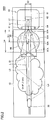
- Fig. 1 is a schematic sectional view of a gas concentration measurement device according to the present embodiment.
- the gas concentration measurement device according to the present embodiment will be described with reference to Fig. 1 .
- a gas concentration measurement device 100 includes a sample cell 10, a light source 20, a band pass filter 41, a detector 60, and a waveguide member 90.
- the gas concentration measurement device 100 measures a gas concentration in accordance with the absorbance of sample gas that flows through a space between the light source 20, which emits infrared light, and the detector 60, which includes a light-receiving portion 62 that receives the infrared light.
- the sample cell 10 includes a sample-gas flow space and allows the sample gas to flow therethrough.
- a sample-gas introduction hole (not shown) is connected to one end of the sample cell 10 (end close to the light source 20), and a sample-gas discharge hole (not shown) is connected to the other end of the sample cell 10 (end close to the detector 60).
- the sample gas introduced into the sample cell 10 through the sample-gas introduction hole is discharged through the sample-gas discharge hole.
- the sample cell 10 contains the light source 20, the waveguide member 90, the band pass filter 41, and the detector 60.
- the light source 20, the waveguide member 90, the band pass filter 41, and the detector 60 are arranged, for example, in that order from one end of the sample cell 10 (from the left side in the figure).
- the light source 20 emits infrared light.
- the light source 20 may be, for example, a filament lamp or an LED lamp that emits wide-band infrared light including desired infrared light. Part of the infrared light emitted from the light source 20 is absorbed depending on infrared light absorption wavelength characteristics of the sample gas.
- the sample gas is, for example, carbon dioxide, and the absorption band thereof is about 4.3 ⁇ m.
- the waveguide member 90 includes a wave-guiding portion 93 having a tubular inner peripheral surface; an entrance portion 91 that is formed at one end of the wave-guiding portion 93 and through which the infrared light from the light source 20 is introduced; and an exit portion 92 that is formed at the other end of the wave-guiding portion 93 and guides the infrared light that has passed through the wave-guiding portion 93 toward the detector 60.
- the waveguide member 90 guides the infrared light toward the detector 60 after part of the infrared light is absorbed by the sample gas.
- the inner peripheral surface of the wave-guiding portion 93 includes a tapered region having a cross-sectional area that decreases from the entrance portion 91 toward the exit portion 92.
- the tapered region has a truncated conical or pyramidal shape whose circumference decreases from the entrance portion 91 toward the exit portion 92.
- the truncated conical or pyramidal shape includes a truncated conical shape and a truncated polygonal pyramidal shape.
- the waveguide member 90 may be made of a resin material, such as acrylonitrile butadiene styrene copolymer synthetic resin (ABS resin) or polycarbonate resin (PC resin).
- ABS resin acrylonitrile butadiene styrene copolymer synthetic resin
- PC resin polycarbonate resin
- the waveguide member 90 is preferably made of a resin material having a reflectance of 20% or less in the infrared range.
- the band pass filter 41 is provided at an end of the detector 60 that is adjacent to the waveguide member 90.
- the band pass filter 41 is securely fitted in a recess 64 formed in a surface of the detector 60 that faces the waveguide member 90.
- the band pass filter 41 is configured to transmit the infrared light in an absorption band of the sample gas to be detected. Thus, only the infrared light having a desired wavelength band reaches the detector 60.
- the detector 60 may be an infrared light detector, such as a thermopile or a bolometer.
- the detector 60 includes a main portion 61, a light-receiving portion 62, and the recess 64.
- the light-receiving portion 62 is embedded in the main portion 61.
- the light-receiving portion 62 receives the infrared light guided out of the exit portion 92 of the waveguide member 90 through the band pass filter 41.
- the detector 60 is electrically connected to a signal processing circuit board (not shown).
- the detector 60 outputs an output signal to the signal processing circuit board based on the infrared light received by the light-receiving portion 62.
- the signal processing circuit board calculates the concentration of the sample gas based on the output signal.
- the transmission band of the band pass filter 41 shifts toward the short-wavelength side as the incident angle increases.
- the measurement accuracy decreases when the transmission band varies. Therefore, when the measurement is performed, the incident angle of the infrared light incident on the band pass filter 41 is preferably small.
- the waveguide member 90 is provided to suppress the influence on the measurement accuracy of the infrared light that is incident on the band pass filter 41 located at the transmitting position at a large incident angle.
- the infrared light L1 is light having a truncated conical or pyramidal shape that linearly travels along the peripheral surface of the wave-guiding portion 93 toward the detector 60.
- the infrared light L2 is light having a shape including two truncated cones obtained by rotating, for example, a ray of light that linearly travels from the bottom end of the entrance portion 91 of the waveguide member 90 in Fig. 1 to the top end of the light-receiving portion 62 in Fig. 1 , one turn along the opening shape of the entrance portion 91.
- the infrared light that linearly travels through the region that is the logical sum of the region surrounded by the outermost rays of the infrared light L1 and the region surrounded by the outermost rays of the infrared light L2 passes through the band pass filter 41 at a relatively small angle.
- Infrared light L4 and infrared light L5 enter the wave-guiding portion 93 through the entrance portion 91 at a relatively large angle with respect to the axial direction of the wave-guiding portion 93.
- the infrared light L4 and the infrared light L5 travel toward the detector 60 while being reflected by the inner peripheral surface of the wave-guiding portion 93 a plurality of times.
- the infrared light L4 and the infrared light L5 may be incident on the band pass filter 41 at a large incident angle.
- the waveguide member 90 is made of a resin material having a reflectance of 20% or less. Therefore, the infrared light L4 and the infrared light L5 are absorbed and attenuated by being repeatedly reflected in the wave-guiding portion 93. For example, in the case where the reflectance of the material is 10%, the attenuation effect obtained when the infrared light is reflected five times is similar to that obtained when the infrared light is reflected once by a component having a reflectance of 0.001%.
- the number of times the infrared light L4 and the infrared light L5 are reflected can be increased by setting an opening area S1 of the entrance portion 91 of the waveguide member 90 greater than an opening area S2 of the exit portion 92 and forming the wave-guiding portion 93 so that the wave-guiding portion 93 includes a tapered region.
- the waveguide member 90 repeatedly reflects the infrared light that has entered the wave-guiding portion 93 through the entrance portion 91 in the tapered region, thereby reducing the energy of the infrared light that is obliquely incident on the band pass filter 41. Accordingly, the measurement accuracy of the gas concentration measurement device can be increased.
- the waveguide member 90 since the waveguide member 90 is provided, the energy of the obliquely incident infrared light can be reduced. Therefore, the measurement accuracy of the gas concentration measurement device 100 can be increased.
- sample gas is carbon dioxide in the present embodiment, the sample gas is not limited to this, and may instead be, for example, carbon monoxide, CH 4 , or NO x .
- Fig. 2 is a schematic sectional view of a gas concentration measurement device according to the present embodiment.
- a gas concentration measurement device 100A according to the present embodiment will be described with reference to Fig. 2 .
- the gas concentration measurement device 100A includes a waveguide member 90A including a wave-guiding portion 93A having a shape that differs from that in the gas concentration measurement device 100 according to the first embodiment.
- Other structures are substantially the same as those in the first embodiment.
- an opening area S1 of an entrance portion 91A is greater than an opening area S2 of an exit portion 92A.
- the internal shape of the wave-guiding portion 93A is partially spherical. A portion of the inner peripheral surface of the wave-guiding portion 93A that forms a portion of a spherical surface is located between the entrance portion 91A and the exit portion 92A.
- the portion that forms a portion of a spherical surface includes a first spherical surface portion 95, which extends toward the exit portion 92A from a boundary at the center M of the sphere, and a second spherical surface portion 96, which extends toward the entrance portion 91A from the boundary at the center M.
- the region from the first spherical surface portion 95 to the exit portion 92A corresponds to a tapered region having a cross-sectional area that decreases along the direction from the entrance portion 91A to the exit portion 92A, and also corresponds to a first curved portion having a circumference that decreases along the direction from the entrance portion 91A to the exit portion 92A.
- the second spherical surface portion 96 corresponds to a second curved portion having a circumference that decreases along the direction from the exit portion 92A to the entrance portion 91A.
- the infrared light that linearly travels through the region that is the logical sum of the region surrounded by the outermost rays of infrared light L1 and the region surrounded by the outermost rays of infrared light L2 mainly reaches the light-receiving portion 62.
- the infrared light L1 is light having a truncated conical or pyramidal shape that linearly travels along the peripheral surfaces of the entrance portion 91A and the exit portion 92A toward the detector 60.
- the infrared light L2 is similar to that in the first embodiment.
- Infrared light L4 and infrared light L5 that have entered the wave-guiding portion 93A through the entrance portion 91A at a relatively large angle with respect to the axial direction of the wave-guiding portion 93A are reflected by the first spherical surface portion 95 and the second spherical surface portion 96 a plurality of times and are emitted from the entrance portion 91A.
- the infrared light L4 and the infrared light L5 emitted from the entrance portion 91A are not incident on the band pass filter 41.
- the distance Lb from the first spherical surface portion 95 to the exit portion 92A in the axial direction of the wave-guiding portion 93A is preferably greater than or equal to half the length La of the waveguide member 90.
- the energy of the infrared light that is obliquely incident on the band pass filter 41 can be reduced, and part of the obliquely incident infrared light can be emitted from the entrance portion 91A. Accordingly, the measurement accuracy of the gas concentration measurement device 100A can be further increased.
- Fig. 3 is a schematic sectional view of a gas concentration measurement device according to the present embodiment.
- a gas concentration measurement device 100B according to the present embodiment will be described with reference to Fig. 3 .
- the gas concentration measurement device 100B includes a waveguide member 90B including a wave-guiding portion 93B having a shape that differs from that in the gas concentration measurement device 100 according to the first embodiment.
- Other structures are substantially the same as those in the first embodiment.
- an opening area S1 of an entrance portion 91B is greater than an opening area S2 of an exit portion 92B.
- the internal shape of the wave-guiding portion 93B includes a first curved portion 93B1 and a second curved portion 93B2.
- the wave-guiding portion 93B includes a maximum circumference portion 94B. The maximum circumference portion 94B is located between the entrance portion 91B and the exit portion 92B.
- the first curved portion 93B1 defines the internal shape of the wave-guiding portion 93B in a region from the maximum circumference portion 94B to the exit portion 92B.
- the first curved portion 93B1 has a circumference that decreases along the direction from the entrance portion 91B to the exit portion 92B.
- the second curved portion 93B2 defines the internal shape of the wave-guiding portion 93B in a region from the maximum circumference portion 94B to the entrance portion 91B.
- the second curved portion 93B2 has a circumference that decreases along the direction from the exit portion 92B to the entrance portion 91B.
- the infrared light that linearly travels through the region that is the logical sum of the region surrounded by the outermost rays of infrared light L1 and the region surrounded by the outermost rays of infrared light L2 mainly reaches the light-receiving portion 62.
- the infrared light L1 is light having a truncated conical or pyramidal shape that linearly travels along the peripheral edges of the entrance portion 91B and the exit portion 92B toward the detector 60.
- the infrared light L2 is similar to that in the first embodiment.
- the length Lb of the first curved portion 93B1 in the axial direction of the waveguide member 90B is preferably greater than or equal to half the length La of the waveguide member 90B in the axial direction.
- infrared light L4 and infrared light L5 which enter through the entrance portion 91B at a relatively large angle with respect to the axial direction of the wave-guiding portion 93B, are reflected a plurality of times in the first curved portion 93B1 and the second curved portion 93B2 and emitted from the entrance portion 91B.
- the energy of the infrared light that is obliquely incident on the band pass filter 41 can be reliably reduced.
- the measurement accuracy of the gas concentration measurement device 100B can be increased.
- Fig. 4 is a schematic sectional view of a gas concentration measurement device according to the present embodiment.
- a gas concentration measurement device 100C according to the present embodiment will be described with reference to Fig. 4 .
- the gas concentration measurement device 100C includes a waveguide member 90C including a wave-guiding portion 93C having a shape that differs from that in the gas concentration measurement device 100 according to the first embodiment.
- Other structures are substantially the same as those in the first embodiment.
- an opening area S1 of an entrance portion 91C is greater than an opening area S2 of an exit portion 92C.
- the internal shape of the wave-guiding portion 93C includes a first truncated conical or pyramidal portion 93C1 and a second truncated conical or pyramidal portion 93C2.
- the wave-guiding portion 93C includes a maximum circumference portion 94C. The maximum circumference portion 94C is located between the entrance portion 91C and the exit portion 92C.
- the first truncated conical or pyramidal portion 93C1 defines the internal shape of the wave-guiding portion 93C in a region from the maximum circumference portion 94C to the exit portion 92C.
- the first truncated conical or pyramidal portion 93C1 has a circumference that decreases along the direction from the entrance portion 91C to the exit portion 92C.
- the second truncated conical or pyramidal portion 93C2 defines the internal shape of the wave-guiding portion 93C in a region from the maximum circumference portion 94C to the entrance portion 91C.
- the second truncated conical or pyramidal portion 93C2 has a circumference that decreases along the direction from the exit portion 92C to the entrance portion 91C.
- the infrared light that linearly travels through the region that is the logical sum of the region surrounded by the outermost rays of infrared light L1 and the region surrounded by the outermost rays of infrared light L2 mainly reaches the light-receiving portion 62.
- the infrared light L1 is light having a truncated conical or pyramidal shape that linearly travels along the peripheral edges of the entrance portion 91C and the exit portion 92C toward the detector 60.
- the infrared light L2 is similar to that in the first embodiment.
- the length Lb of the first truncated conical or pyramidal portion 93C1 in the axial direction of the waveguide member 90C is preferably greater than or equal to half the length La of the waveguide member 90C in the axial direction.
- infrared light L4 for example, which enters through the entrance portion 91C at a relatively large angle with respect to the axial direction of the wave-guiding portion 93C, is reflected a plurality of times in the first truncated conical or pyramidal portion 93C1 and the second truncated conical or pyramidal portion 93C2.
- the energy of the infrared light that is obliquely incident on the band pass filter 41 can be reliably reduced.
- the measurement accuracy of the gas concentration measurement device can be increased.
- Fig. 5 is a schematic sectional view of a gas concentration measurement device according to the present embodiment.
- a gas concentration measurement device 100D according to the present embodiment will be described with reference to Fig. 5 .
- the gas concentration measurement device 100D includes a waveguide member 90D including a wave-guiding portion 93D having a shape that differs from that in the gas concentration measurement device 100C according to the fourth embodiment.
- an opening area S1 of an entrance portion 91D is greater than an opening area S2 of an exit portion 92D.
- the internal shape of the wave-guiding portion 93D includes a truncated conical or pyramidal portion 93D1 and a columnar portion 93D2.
- the shape of the truncated conical or pyramidal portion 93D1 is substantially the same as that of the first truncated conical or pyramidal portion 93C1 according to the fourth embodiment.
- the relationship between the length of the truncated conical or pyramidal portion 93D1 and the length of the waveguide member 90D is also similar to the relationship between the length of the first truncated conical or pyramidal portion 93C1 and the length of the waveguide member 90C according to the fourth embodiment.
- the columnar portion 93D2 is configured so that the circumference thereof is constant over a region from the entrance portion 91D to the upstream end of the truncated conical or pyramidal portion 93D1.
- the circumference of the columnar portion 93D2 is equal to the maximum circumference.
- infrared light L4 and infrared light L5 which enter through the entrance portion 91D at a relatively large angle with respect to the axial direction of the wave-guiding portion 93D, is reflected a plurality of times in the truncated conical or pyramidal portion 93D1 and the columnar portion 93D2.
- the energy of the infrared light that is obliquely incident on the band pass filter 41 can be reliably reduced.
- the measurement accuracy of the gas concentration measurement device can be increased.
- the columnar portion is arranged adjacent to the entrance portion 91D, and the truncated conical or pyramidal portion is arranged adjacent to the exit portion 92D.
- the arrangement is not limited to this, and the columnar portion may be arranged adjacent to the exit portion 92D while the truncated conical or pyramidal portion is arranged adjacent to the entrance portion 91D.
- the circumference of the columnar portion is set to the minimum circumference.
- a portion that connects the entrance portion 91A to the upstream end of the second spherical surface portion 96 (first connecting portion) and a portion that connects the downstream end of the first spherical surface portion 95 to the exit portion 92A (second connecting portion) have circumferences that decrease along the direction from the entrance portion 91A to the exit portion 92A.
- the first and second connecting portions are not limited to this, and at least one of the first and second connecting portions may have a columnar shape with a constant circumference.
- the second curved portion 93B2 is provided so as to extend from the entrance portion 91B to the maximum circumference portion 94B.
- the second curved portion 93B2 may be replaced by a columnar portion having a circumference that is constant over a region from the entrance portion 91B to the maximum circumference portion 94B.
Landscapes
- Chemical & Material Sciences (AREA)
- Physics & Mathematics (AREA)
- Health & Medical Sciences (AREA)
- Life Sciences & Earth Sciences (AREA)
- Immunology (AREA)
- Biochemistry (AREA)
- General Health & Medical Sciences (AREA)
- General Physics & Mathematics (AREA)
- Analytical Chemistry (AREA)
- Pathology (AREA)
- Engineering & Computer Science (AREA)
- Spectroscopy & Molecular Physics (AREA)
- Combustion & Propulsion (AREA)
- Food Science & Technology (AREA)
- Medicinal Chemistry (AREA)
- Investigating Or Analysing Materials By Optical Means (AREA)
Abstract
Description
- The present invention relates to an infrared-light-absorption gas concentration measurement device.
- Various types of gas concentration measurement devices for analyzing various types of exhaust, gas contained in the atmosphere, or gas contained in the air in a building have been developed. In particular, infrared-light-absorption gas concentration measurement devices are used to analyze sample gas by utilizing the fact that the sample gas absorbs infrared light in a specific wavelength range.
- International Publication No.
01/27596 Patent Document 1, an anti-reflection film is applied to inner walls of an analysis chamber (sample cell) that defines a flow channel for the sample gas. Accordingly, the risk that the infrared light will be incident on a band pass filter, which is provided on a surface of a detector, at an angle greater than a predetermined angle is reduced. - Patent Document 1: International Publication No.
01/27596 - The anti-reflection film disclosed in
Patent Document 1 needs to be made of a material having a reflectance close to zero. Thus, the material of the anti-reflection film is limited. If an inexpensive material having a reflectance that is not close to zero is used, the infrared light is reflected by the anti-reflection film and is incident on the band pass filter at an angle greater than the predetermined angle. In such a case, the transmission band of the band pass filter is shifted and the measurement accuracy decreases. - Therefore, there is a need for a gas concentration measurement device having a new structure that can be substituted for the anti-reflection film made of a specified material and that can reduce the risk that the infrared light will be incident on the band pass filter at an angle greater than the predetermined angle.
- The present invention has been made in light of the above-described problem, and an object of the present invention is to provide a gas concentration measurement device capable of increasing the measurement accuracy. Solution to Problem
- A gas concentration measurement device according to the present invention includes a light source that emits infrared light; a detector that detects the infrared light from the light source through a band pass filter; and a waveguide member including a wave-guiding portion having a tubular inner peripheral surface, an entrance portion that is formed at one side of the wave-guiding portion and through which the infrared light from the light source is introduced, and an exit portion that is formed at the other side of the wave-guiding portion and guides the infrared light that has passed through the wave-guiding portion toward the detector. A portion or entirety of the inner peripheral surface of the wave-guiding portion includes a tapered region having a cross section that decreases along a direction from the entrance portion to the exit portion. The waveguide member reflects the infrared light that has entered the wave-guiding portion through the entrance portion in the tapered region, so that energy of the infrared light that is obliquely incident on the band pass filter is reduced.
- In the gas concentration measurement device according to the present invention, preferably, the tapered region of the inner peripheral surface of the wave-guiding portion includes a truncated conical or pyramidal portion having a perimeter that decreases along a direction from the entrance portion to the exit portion.
- In the gas concentration measurement device according to the present invention, preferably, an opening area of the entrance portion is greater than an opening area of the exit portion.
- In the gas concentration measurement device according to the present invention, preferably, the tapered region of the inner peripheral surface of the wave-guiding portion includes a first curved portion having a perimeter that decreases along a direction from the entrance portion to the exit portion.
- In the gas concentration measurement device according to the present invention, preferably, a length of the first curved portion in an axial direction of the wave-guiding portion is greater than or equal to half a length of the wave-guiding portion in the axial direction of the wave-guiding portion.
- In the gas concentration measurement device according to the present invention, preferably, the inner peripheral surface of the wave-guiding portion includes a second curved portion having a perimeter that decreases along a direction from the exit portion to the entrance portion.
- In the gas concentration measurement device according to the present invention, preferably, the waveguide member is made of a resin material.
- According to the present invention, a gas concentration measurement device capable of increasing the measurement accuracy can be provided.
-
- [
Fig. 1] Fig. 1 is a schematic sectional view of a gas concentration measurement device according to a first embodiment. - [
Fig. 2] Fig. 2 is a schematic sectional view of a gas concentration measurement device according to a second embodiment. - [
Fig. 3] Fig. 3 is a schematic sectional view of a gas concentration measurement device according to a third embodiment. - [
Fig. 4] Fig. 4 is a schematic sectional view of a gas concentration measurement device according to a fourth embodiment. - [
Fig. 5] Fig. 5 is a schematic sectional view of a gas concentration measurement device according to a fifth embodiment. - Embodiments of the present invention will be described in detail with reference to the drawings. In the embodiments described below, components that are the same or similar are denoted by the same reference numerals in the drawings, and descriptions thereof will not be repeated.
-
Fig. 1 is a schematic sectional view of a gas concentration measurement device according to the present embodiment. The gas concentration measurement device according to the present embodiment will be described with reference toFig. 1 . - As illustrated in
Fig. 1 , a gasconcentration measurement device 100 according to the present embodiment includes asample cell 10, alight source 20, aband pass filter 41, adetector 60, and awaveguide member 90. The gasconcentration measurement device 100 measures a gas concentration in accordance with the absorbance of sample gas that flows through a space between thelight source 20, which emits infrared light, and thedetector 60, which includes a light-receivingportion 62 that receives the infrared light. - The
sample cell 10 includes a sample-gas flow space and allows the sample gas to flow therethrough. For example, a sample-gas introduction hole (not shown) is connected to one end of the sample cell 10 (end close to the light source 20), and a sample-gas discharge hole (not shown) is connected to the other end of the sample cell 10 (end close to the detector 60). The sample gas introduced into thesample cell 10 through the sample-gas introduction hole is discharged through the sample-gas discharge hole. - The
sample cell 10 contains thelight source 20, thewaveguide member 90, theband pass filter 41, and thedetector 60. Thelight source 20, thewaveguide member 90, theband pass filter 41, and thedetector 60 are arranged, for example, in that order from one end of the sample cell 10 (from the left side in the figure). - The
light source 20 emits infrared light. Thelight source 20 may be, for example, a filament lamp or an LED lamp that emits wide-band infrared light including desired infrared light. Part of the infrared light emitted from thelight source 20 is absorbed depending on infrared light absorption wavelength characteristics of the sample gas. The sample gas is, for example, carbon dioxide, and the absorption band thereof is about 4.3 µm. - The
waveguide member 90 includes a wave-guidingportion 93 having a tubular inner peripheral surface; anentrance portion 91 that is formed at one end of the wave-guidingportion 93 and through which the infrared light from thelight source 20 is introduced; and anexit portion 92 that is formed at the other end of the wave-guidingportion 93 and guides the infrared light that has passed through the wave-guidingportion 93 toward thedetector 60. Thewaveguide member 90 guides the infrared light toward thedetector 60 after part of the infrared light is absorbed by the sample gas. - The inner peripheral surface of the wave-guiding
portion 93 includes a tapered region having a cross-sectional area that decreases from theentrance portion 91 toward theexit portion 92. The tapered region has a truncated conical or pyramidal shape whose circumference decreases from theentrance portion 91 toward theexit portion 92. The truncated conical or pyramidal shape includes a truncated conical shape and a truncated polygonal pyramidal shape. - The
waveguide member 90 may be made of a resin material, such as acrylonitrile butadiene styrene copolymer synthetic resin (ABS resin) or polycarbonate resin (PC resin). In particular, thewaveguide member 90 is preferably made of a resin material having a reflectance of 20% or less in the infrared range. - The
band pass filter 41 is provided at an end of thedetector 60 that is adjacent to thewaveguide member 90. Theband pass filter 41 is securely fitted in arecess 64 formed in a surface of thedetector 60 that faces thewaveguide member 90. - The
band pass filter 41 is configured to transmit the infrared light in an absorption band of the sample gas to be detected. Thus, only the infrared light having a desired wavelength band reaches thedetector 60. - The
detector 60 may be an infrared light detector, such as a thermopile or a bolometer. Thedetector 60 includes amain portion 61, a light-receivingportion 62, and therecess 64. The light-receivingportion 62 is embedded in themain portion 61. The light-receivingportion 62 receives the infrared light guided out of theexit portion 92 of thewaveguide member 90 through theband pass filter 41. - The
detector 60 is electrically connected to a signal processing circuit board (not shown). Thedetector 60 outputs an output signal to the signal processing circuit board based on the infrared light received by the light-receivingportion 62. The signal processing circuit board calculates the concentration of the sample gas based on the output signal. - The infrared light incident on the
band pass filter 41 will now be described. In general, the transmission band of theband pass filter 41 shifts toward the short-wavelength side as the incident angle increases. The measurement accuracy decreases when the transmission band varies. Therefore, when the measurement is performed, the incident angle of the infrared light incident on theband pass filter 41 is preferably small. - In the present embodiment, the
waveguide member 90 is provided to suppress the influence on the measurement accuracy of the infrared light that is incident on theband pass filter 41 located at the transmitting position at a large incident angle. - The infrared light that linearly travels through the region that is the logical sum of the region surrounded by the outermost rays of infrared light L1 and the region surrounded by the outermost rays of infrared light L2 (for example, arrow L in
Fig. 1 ) mainly reaches the light-receivingportion 62 through theband pass filter 41. The infrared light L1 is light having a truncated conical or pyramidal shape that linearly travels along the peripheral surface of the wave-guidingportion 93 toward thedetector 60. The infrared light L2 is light having a shape including two truncated cones obtained by rotating, for example, a ray of light that linearly travels from the bottom end of theentrance portion 91 of thewaveguide member 90 inFig. 1 to the top end of the light-receivingportion 62 inFig. 1 , one turn along the opening shape of theentrance portion 91. - The infrared light that linearly travels through the region that is the logical sum of the region surrounded by the outermost rays of the infrared light L1 and the region surrounded by the outermost rays of the infrared light L2 passes through the
band pass filter 41 at a relatively small angle. - Infrared light L4 and infrared light L5 enter the wave-guiding
portion 93 through theentrance portion 91 at a relatively large angle with respect to the axial direction of the wave-guidingportion 93. The infrared light L4 and the infrared light L5 travel toward thedetector 60 while being reflected by the inner peripheral surface of the wave-guiding portion 93 a plurality of times. - If it is assumed that the reflectance of the wave-guiding
portion 93 is 100%, the infrared light L4 and the infrared light L5 may be incident on theband pass filter 41 at a large incident angle. - In the present embodiment, the
waveguide member 90 is made of a resin material having a reflectance of 20% or less. Therefore, the infrared light L4 and the infrared light L5 are absorbed and attenuated by being repeatedly reflected in the wave-guidingportion 93. For example, in the case where the reflectance of the material is 10%, the attenuation effect obtained when the infrared light is reflected five times is similar to that obtained when the infrared light is reflected once by a component having a reflectance of 0.001%. The number of times the infrared light L4 and the infrared light L5 are reflected can be increased by setting an opening area S1 of theentrance portion 91 of thewaveguide member 90 greater than an opening area S2 of theexit portion 92 and forming the wave-guidingportion 93 so that the wave-guidingportion 93 includes a tapered region. - Thus, the
waveguide member 90 repeatedly reflects the infrared light that has entered the wave-guidingportion 93 through theentrance portion 91 in the tapered region, thereby reducing the energy of the infrared light that is obliquely incident on theband pass filter 41. Accordingly, the measurement accuracy of the gas concentration measurement device can be increased. - As described above, in the gas
concentration measurement device 100 according to the present embodiment, since thewaveguide member 90 is provided, the energy of the obliquely incident infrared light can be reduced. Therefore, the measurement accuracy of the gasconcentration measurement device 100 can be increased. - Although the sample gas is carbon dioxide in the present embodiment, the sample gas is not limited to this, and may instead be, for example, carbon monoxide, CH4, or NOx.
-
Fig. 2 is a schematic sectional view of a gas concentration measurement device according to the present embodiment. A gasconcentration measurement device 100A according to the present embodiment will be described with reference toFig. 2 . - As illustrated in
Fig. 2 , the gasconcentration measurement device 100A according to the present embodiment includes awaveguide member 90A including a wave-guidingportion 93A having a shape that differs from that in the gasconcentration measurement device 100 according to the first embodiment. Other structures are substantially the same as those in the first embodiment. - Also in the
waveguide member 90A, an opening area S1 of anentrance portion 91A is greater than an opening area S2 of anexit portion 92A. The internal shape of the wave-guidingportion 93A is partially spherical. A portion of the inner peripheral surface of the wave-guidingportion 93A that forms a portion of a spherical surface is located between theentrance portion 91A and theexit portion 92A. - The portion that forms a portion of a spherical surface includes a first
spherical surface portion 95, which extends toward theexit portion 92A from a boundary at the center M of the sphere, and a secondspherical surface portion 96, which extends toward theentrance portion 91A from the boundary at the center M. The region from the firstspherical surface portion 95 to theexit portion 92A corresponds to a tapered region having a cross-sectional area that decreases along the direction from theentrance portion 91A to theexit portion 92A, and also corresponds to a first curved portion having a circumference that decreases along the direction from theentrance portion 91A to theexit portion 92A. The secondspherical surface portion 96 corresponds to a second curved portion having a circumference that decreases along the direction from theexit portion 92A to theentrance portion 91A. - Also when the wave-guiding
portion 93A has the above-described shape, the infrared light that linearly travels through the region that is the logical sum of the region surrounded by the outermost rays of infrared light L1 and the region surrounded by the outermost rays of infrared light L2 (for example, arrow L inFig. 2 ) mainly reaches the light-receivingportion 62. The infrared light L1 is light having a truncated conical or pyramidal shape that linearly travels along the peripheral surfaces of theentrance portion 91A and theexit portion 92A toward thedetector 60. The infrared light L2 is similar to that in the first embodiment. - Infrared light L4 and infrared light L5 that have entered the wave-guiding
portion 93A through theentrance portion 91A at a relatively large angle with respect to the axial direction of the wave-guidingportion 93A are reflected by the firstspherical surface portion 95 and the second spherical surface portion 96 a plurality of times and are emitted from theentrance portion 91A. - The infrared light L4 and the infrared light L5 emitted from the
entrance portion 91A are not incident on theband pass filter 41. To increase the number of times the light is reflected by the wave-guidingportion 93A, the distance Lb from the firstspherical surface portion 95 to theexit portion 92A in the axial direction of the wave-guidingportion 93A is preferably greater than or equal to half the length La of thewaveguide member 90. - Thus, in the present embodiment, the energy of the infrared light that is obliquely incident on the
band pass filter 41 can be reduced, and part of the obliquely incident infrared light can be emitted from theentrance portion 91A. Accordingly, the measurement accuracy of the gasconcentration measurement device 100A can be further increased. -
Fig. 3 is a schematic sectional view of a gas concentration measurement device according to the present embodiment. A gasconcentration measurement device 100B according to the present embodiment will be described with reference toFig. 3 . - As illustrated in
Fig. 3 , the gasconcentration measurement device 100B according to the present embodiment includes awaveguide member 90B including a wave-guidingportion 93B having a shape that differs from that in the gasconcentration measurement device 100 according to the first embodiment. Other structures are substantially the same as those in the first embodiment. - Also in the
waveguide member 90B, an opening area S1 of anentrance portion 91B is greater than an opening area S2 of anexit portion 92B. The internal shape of the wave-guidingportion 93B includes a first curved portion 93B1 and a second curved portion 93B2. The wave-guidingportion 93B includes amaximum circumference portion 94B. Themaximum circumference portion 94B is located between theentrance portion 91B and theexit portion 92B. - The first curved portion 93B1 defines the internal shape of the wave-guiding
portion 93B in a region from themaximum circumference portion 94B to theexit portion 92B. The first curved portion 93B1 has a circumference that decreases along the direction from theentrance portion 91B to theexit portion 92B. - The second curved portion 93B2 defines the internal shape of the wave-guiding
portion 93B in a region from themaximum circumference portion 94B to theentrance portion 91B. The second curved portion 93B2 has a circumference that decreases along the direction from theexit portion 92B to theentrance portion 91B. - Also in this case, the infrared light that linearly travels through the region that is the logical sum of the region surrounded by the outermost rays of infrared light L1 and the region surrounded by the outermost rays of infrared light L2 mainly reaches the light-receiving
portion 62. The infrared light L1 is light having a truncated conical or pyramidal shape that linearly travels along the peripheral edges of theentrance portion 91B and theexit portion 92B toward thedetector 60. The infrared light L2 is similar to that in the first embodiment. - The length Lb of the first curved portion 93B1 in the axial direction of the
waveguide member 90B is preferably greater than or equal to half the length La of thewaveguide member 90B in the axial direction. When this length relationship is satisfied, infrared light L4 and infrared light L5, which enter through theentrance portion 91B at a relatively large angle with respect to the axial direction of the wave-guidingportion 93B, are reflected a plurality of times in the first curved portion 93B1 and the second curved portion 93B2 and emitted from theentrance portion 91B. - Accordingly, also in the present embodiment, the energy of the infrared light that is obliquely incident on the
band pass filter 41 can be reliably reduced. As a result, the measurement accuracy of the gasconcentration measurement device 100B can be increased. -
Fig. 4 is a schematic sectional view of a gas concentration measurement device according to the present embodiment. A gasconcentration measurement device 100C according to the present embodiment will be described with reference toFig. 4 . - As illustrated in
Fig. 4 , the gasconcentration measurement device 100C according to the present embodiment includes awaveguide member 90C including a wave-guidingportion 93C having a shape that differs from that in the gasconcentration measurement device 100 according to the first embodiment. Other structures are substantially the same as those in the first embodiment. - Also in the
waveguide member 90C, an opening area S1 of anentrance portion 91C is greater than an opening area S2 of anexit portion 92C. The internal shape of the wave-guidingportion 93C includes a first truncated conical or pyramidal portion 93C1 and a second truncated conical or pyramidal portion 93C2. The wave-guidingportion 93C includes amaximum circumference portion 94C. Themaximum circumference portion 94C is located between theentrance portion 91C and theexit portion 92C. - The first truncated conical or pyramidal portion 93C1 defines the internal shape of the wave-guiding
portion 93C in a region from themaximum circumference portion 94C to theexit portion 92C. The first truncated conical or pyramidal portion 93C1 has a circumference that decreases along the direction from theentrance portion 91C to theexit portion 92C. - The second truncated conical or pyramidal portion 93C2 defines the internal shape of the wave-guiding
portion 93C in a region from themaximum circumference portion 94C to theentrance portion 91C. The second truncated conical or pyramidal portion 93C2 has a circumference that decreases along the direction from theexit portion 92C to theentrance portion 91C. - Also in this case, the infrared light that linearly travels through the region that is the logical sum of the region surrounded by the outermost rays of infrared light L1 and the region surrounded by the outermost rays of infrared light L2 mainly reaches the light-receiving
portion 62. The infrared light L1 is light having a truncated conical or pyramidal shape that linearly travels along the peripheral edges of theentrance portion 91C and theexit portion 92C toward thedetector 60. The infrared light L2 is similar to that in the first embodiment. - The length Lb of the first truncated conical or pyramidal portion 93C1 in the axial direction of the
waveguide member 90C is preferably greater than or equal to half the length La of thewaveguide member 90C in the axial direction. When this length relationship is satisfied, infrared light L4, for example, which enters through theentrance portion 91C at a relatively large angle with respect to the axial direction of the wave-guidingportion 93C, is reflected a plurality of times in the first truncated conical or pyramidal portion 93C1 and the second truncated conical or pyramidal portion 93C2. - Accordingly, also in the gas
concentration measurement device 100C according to the present embodiment, the energy of the infrared light that is obliquely incident on theband pass filter 41 can be reliably reduced. As a result, the measurement accuracy of the gas concentration measurement device can be increased. -
Fig. 5 is a schematic sectional view of a gas concentration measurement device according to the present embodiment. A gasconcentration measurement device 100D according to the present embodiment will be described with reference toFig. 5 . - As illustrated in
Fig. 5 , the gasconcentration measurement device 100D according to the present embodiment includes awaveguide member 90D including a wave-guidingportion 93D having a shape that differs from that in the gasconcentration measurement device 100C according to the fourth embodiment. - Also in the
waveguide member 90D, an opening area S1 of anentrance portion 91D is greater than an opening area S2 of anexit portion 92D. The internal shape of the wave-guidingportion 93D includes a truncated conical or pyramidal portion 93D1 and a columnar portion 93D2. The shape of the truncated conical or pyramidal portion 93D1 is substantially the same as that of the first truncated conical or pyramidal portion 93C1 according to the fourth embodiment. The relationship between the length of the truncated conical or pyramidal portion 93D1 and the length of thewaveguide member 90D is also similar to the relationship between the length of the first truncated conical or pyramidal portion 93C1 and the length of thewaveguide member 90C according to the fourth embodiment. - The columnar portion 93D2 is configured so that the circumference thereof is constant over a region from the
entrance portion 91D to the upstream end of the truncated conical or pyramidal portion 93D1. The circumference of the columnar portion 93D2 is equal to the maximum circumference. - Also in this case, infrared light L4 and infrared light L5, which enter through the
entrance portion 91D at a relatively large angle with respect to the axial direction of the wave-guidingportion 93D, is reflected a plurality of times in the truncated conical or pyramidal portion 93D1 and the columnar portion 93D2. - Accordingly, also in the gas
concentration measurement device 100D according to the present embodiment, the energy of the infrared light that is obliquely incident on theband pass filter 41 can be reliably reduced. As a result, the measurement accuracy of the gas concentration measurement device can be increased. - In the present embodiment, the columnar portion is arranged adjacent to the
entrance portion 91D, and the truncated conical or pyramidal portion is arranged adjacent to theexit portion 92D. However, the arrangement is not limited to this, and the columnar portion may be arranged adjacent to theexit portion 92D while the truncated conical or pyramidal portion is arranged adjacent to theentrance portion 91D. In this case, the circumference of the columnar portion is set to the minimum circumference. - In the above-described second embodiment, a portion that connects the
entrance portion 91A to the upstream end of the second spherical surface portion 96 (first connecting portion) and a portion that connects the downstream end of the firstspherical surface portion 95 to theexit portion 92A (second connecting portion) have circumferences that decrease along the direction from theentrance portion 91A to theexit portion 92A. However, the first and second connecting portions are not limited to this, and at least one of the first and second connecting portions may have a columnar shape with a constant circumference. - In the above-described third embodiment, the second curved portion 93B2 is provided so as to extend from the
entrance portion 91B to themaximum circumference portion 94B. However, the second curved portion 93B2 may be replaced by a columnar portion having a circumference that is constant over a region from theentrance portion 91B to themaximum circumference portion 94B. - Although embodiments of the present invention have been described, the embodiments disclosed herein are illustrative and not restrictive in all points. The scope of the present invention is to be defined by the scope of the claims, and includes equivalents to the scope of the claims and all changes within the scope of the claims.
- 10 sample cell, 20 light source, 41 band pass filter, 60 detector, 61 main portion, 62 light-receiving portion, 64 recess, 90, 90A, 90B, 90C, and 90D waveguide member, 91, 91A, 91B, 91C, and 91D entrance portion, 92, 92A, 92B, 92C, and 92D exit portion, 93, 93A, 93B, 93C, and 93D wave-guiding portion, 93B1 first curved portion, 93B2 second curved portion, 93C1 first truncated conical or pyramidal portion, 93C2 second truncated conical or pyramidal portion, 93D1 truncated conical or pyramidal portion, 93D2 columnar portion, 94B and 94C maximum circumference portion, 95 first spherical surface portion, 96 second spherical surface portion, 100, 100A, 100B, 100C, and 100D gas concentration measurement device.
Claims (7)
- A gas concentration measurement device comprising:a light source that emits infrared light;a detector that detects the infrared light from the light source through a band pass filter; anda waveguide member including a wave-guiding portion having a tubular inner peripheral surface, an entrance portion that is formed at one side of the wave-guiding portion and through which the infrared light from the light source is introduced, and an exit portion that is formed at the other side of the wave-guiding portion and guides the infrared light that has passed through the wave-guiding portion toward the detector,wherein a portion or entirety of the inner peripheral surface of the wave-guiding portion includes a tapered region having a cross section that decreases along a direction from the entrance portion to the exit portion, andwherein the waveguide member reflects the infrared light that has entered the wave-guiding portion through the entrance portion in the tapered region, so that energy of the infrared light that is obliquely incident on the band pass filter is reduced.
- The gas concentration measurement device according to Claim 1, wherein the tapered region of the inner peripheral surface of the wave-guiding portion includes a truncated conical or pyramidal portion having a perimeter that decreases along a direction from the entrance portion to the exit portion.
- The gas concentration measurement device according to Claim 1 or 2, wherein an opening area of the entrance portion is greater than an opening area of the exit portion.
- The gas concentration measurement device according to any one of Claims 1 to 3, wherein the tapered region of the inner peripheral surface of the wave-guiding portion includes a first curved portion having a perimeter that decreases along a direction from the entrance portion to the exit portion.
- The gas concentration measurement device according to Claim 4, wherein a length of the first curved portion in an axial direction of the wave-guiding portion is greater than or equal to half a length of the wave-guiding portion in the axial direction of the wave-guiding portion.
- The gas concentration measurement device according to any one of Claims 1 to 5, wherein the inner peripheral surface of the wave-guiding portion includes a second curved portion having a perimeter that decreases along a direction from the exit portion to the entrance portion.
- The gas concentration measurement device according to any one of Claims 1 to 6, wherein the waveguide member is made of a resin material.
Applications Claiming Priority (2)
| Application Number | Priority Date | Filing Date | Title |
|---|---|---|---|
| JP2014137787 | 2014-07-03 | ||
| PCT/JP2015/066873 WO2016002467A1 (en) | 2014-07-03 | 2015-06-11 | Gas concentration measurement device |
Publications (3)
| Publication Number | Publication Date |
|---|---|
| EP3165905A1 true EP3165905A1 (en) | 2017-05-10 |
| EP3165905A4 EP3165905A4 (en) | 2018-02-21 |
| EP3165905B1 EP3165905B1 (en) | 2019-10-02 |
Family
ID=55019016
Family Applications (1)
| Application Number | Title | Priority Date | Filing Date |
|---|---|---|---|
| EP15815028.4A Active EP3165905B1 (en) | 2014-07-03 | 2015-06-11 | Gas concentration measurement device |
Country Status (4)
| Country | Link |
|---|---|
| US (1) | US10254222B2 (en) |
| EP (1) | EP3165905B1 (en) |
| JP (1) | JP6245366B2 (en) |
| WO (1) | WO2016002467A1 (en) |
Families Citing this family (2)
| Publication number | Priority date | Publication date | Assignee | Title |
|---|---|---|---|---|
| JP6556338B2 (en) * | 2016-04-15 | 2019-08-07 | Phcホールディングス株式会社 | Gas sensor and thermostat |
| US10161859B2 (en) | 2016-10-27 | 2018-12-25 | Honeywell International Inc. | Planar reflective ring |
Family Cites Families (23)
| Publication number | Priority date | Publication date | Assignee | Title |
|---|---|---|---|---|
| US4011451A (en) * | 1975-07-03 | 1977-03-08 | Waters Associates, Incorporated | Novel photometric system |
| IE44010B1 (en) * | 1976-02-25 | 1981-07-29 | Rossiter V | Method and apparatus for examining the infrared spectrum of small quantities of materials in the vapour phase |
| US4084909A (en) * | 1976-07-19 | 1978-04-18 | International Business Machines Corporation | Drum monochromator |
| US4736103A (en) * | 1986-03-07 | 1988-04-05 | Westinghouse Electric Corp. | Spectrometer test gas chamber |
| JPH07236040A (en) * | 1994-02-22 | 1995-09-05 | Nippon Avionics Co Ltd | Color line sensor camera |
| JPH10309281A (en) * | 1997-05-13 | 1998-11-24 | Olympus Optical Co Ltd | Fluorescent diagnostic device |
| JP2004239611A (en) | 1999-10-12 | 2004-08-26 | Nok Corp | Co sensor |
| SE520664C2 (en) * | 2000-04-27 | 2003-08-05 | Senseair Ab | Carbon dioxide-adapted gas cell |
| JP3771849B2 (en) * | 2001-09-27 | 2006-04-26 | 株式会社堀場製作所 | Infrared gas analysis method and apparatus |
| JP2003215037A (en) * | 2002-01-25 | 2003-07-30 | Horiba Ltd | Method and apparatus for hc analysis by ndir method |
| JP3899004B2 (en) * | 2002-09-27 | 2007-03-28 | 株式会社堀場製作所 | In-vehicle HC measuring device |
| US6865472B2 (en) | 2002-09-27 | 2005-03-08 | Horiba Ltd. | Vehicle-installed exhaust gas analyzing apparatus |
| DE10321639A1 (en) * | 2003-05-13 | 2004-12-02 | Heimann Sensor Gmbh | Infrared sensor with optimized use of space |
| JP4663258B2 (en) * | 2003-06-17 | 2011-04-06 | オリンパス株式会社 | Endoscope device |
| JP3991029B2 (en) * | 2003-12-19 | 2007-10-17 | 株式会社日立ハイテクノロジーズ | Nucleic acid analyzer |
| KR100791961B1 (en) * | 2004-12-24 | 2008-01-04 | 코리아디지탈 주식회사 | Waveguide Structure of Non-Dispersive Infrared Gas Measuring System |
| JP2010223610A (en) * | 2009-03-19 | 2010-10-07 | Toyota Central R&D Labs Inc | Self-forming optical waveguide sensor |
| EP2444791B1 (en) * | 2010-10-25 | 2020-04-15 | General Electric Company | Gas analyzer for measuring at least two components of a gas |
| JP5794803B2 (en) | 2011-03-28 | 2015-10-14 | 株式会社堀場エステック | Spectrophotometer and calibration method thereof |
| JP5870270B2 (en) * | 2011-10-24 | 2016-02-24 | パナソニックIpマネジメント株式会社 | Detector |
| JP2013120153A (en) * | 2011-12-08 | 2013-06-17 | Panasonic Corp | Gas component detector |
| JP6333257B2 (en) * | 2012-08-30 | 2018-05-30 | アイティーアイ・スコットランド ‐ スコティッシュ・エンタープライズIti Scotland ‐ Scottish Enterprise | Long-wavelength infrared detection and image processing using a long-wavelength infrared light source |
| CN104797926B (en) * | 2012-11-30 | 2017-12-26 | 松下知识产权经营株式会社 | Optical sensor device and method for producing optical element used in optical sensor device |
-
2015
- 2015-06-11 WO PCT/JP2015/066873 patent/WO2016002467A1/en not_active Ceased
- 2015-06-11 EP EP15815028.4A patent/EP3165905B1/en active Active
- 2015-06-11 JP JP2016531226A patent/JP6245366B2/en active Active
-
2016
- 2016-12-20 US US15/384,362 patent/US10254222B2/en active Active
Also Published As
| Publication number | Publication date |
|---|---|
| JPWO2016002467A1 (en) | 2017-04-27 |
| US10254222B2 (en) | 2019-04-09 |
| EP3165905A4 (en) | 2018-02-21 |
| WO2016002467A1 (en) | 2016-01-07 |
| JP6245366B2 (en) | 2017-12-13 |
| EP3165905B1 (en) | 2019-10-02 |
| US20170102328A1 (en) | 2017-04-13 |
Similar Documents
| Publication | Publication Date | Title |
|---|---|---|
| EP3435073B1 (en) | Optical fiber testing device, optical fiber manufacturing device, optical fiber testing method, and optical fiber manufacturing method | |
| TWI513974B (en) | Detector | |
| US20210055212A1 (en) | Optical gas sensor | |
| CN108709868A (en) | A kind of infrared gas sensor and infrared gas detection device | |
| EP2601512B1 (en) | Annular optical device | |
| US9915604B2 (en) | Gas concentration measurement device | |
| KR20160099620A (en) | ATR infrared spectrometer | |
| EP3165905A1 (en) | Gas concentration measurement device | |
| CN210626326U (en) | Multi-gas concentration detection device and alarm device | |
| US10012585B2 (en) | Gas sampling cell | |
| US10345223B2 (en) | Optical gas sensor | |
| JP2010133833A (en) | Photometric device | |
| CN101949838B (en) | Dispersive infrared absorption gas detection device and method | |
| JP2015031682A (en) | Fluorescence detector | |
| EP4062153B1 (en) | Optical based particulate matter sensing | |
| EP3217163B1 (en) | Analysis device and exhaust gas treatment device | |
| KR20090004271A (en) | Optical gas sensor | |
| KR20240130360A (en) | Optical multi gas detection system | |
| JP2013068461A (en) | Refraction factor measuring apparatus, sugar concentration measuring apparatus and method therefor | |
| JP2015227858A5 (en) | ||
| US9678251B2 (en) | Optical head for receiving light and optical system using the same | |
| KR100791961B1 (en) | Waveguide Structure of Non-Dispersive Infrared Gas Measuring System | |
| WO2019038818A1 (en) | Flow cell | |
| US11175218B2 (en) | Flow cell and detector equipped with the flow cell | |
| US12372457B2 (en) | Optimized infrared light source for a gas sensor, and manufacturing method thereof |
Legal Events
| Date | Code | Title | Description |
|---|---|---|---|
| STAA | Information on the status of an ep patent application or granted ep patent |
Free format text: STATUS: THE INTERNATIONAL PUBLICATION HAS BEEN MADE |
|
| PUAI | Public reference made under article 153(3) epc to a published international application that has entered the european phase |
Free format text: ORIGINAL CODE: 0009012 |
|
| STAA | Information on the status of an ep patent application or granted ep patent |
Free format text: STATUS: REQUEST FOR EXAMINATION WAS MADE |
|
| 17P | Request for examination filed |
Effective date: 20161206 |
|
| AK | Designated contracting states |
Kind code of ref document: A1 Designated state(s): AL AT BE BG CH CY CZ DE DK EE ES FI FR GB GR HR HU IE IS IT LI LT LU LV MC MK MT NL NO PL PT RO RS SE SI SK SM TR |
|
| AX | Request for extension of the european patent |
Extension state: BA ME |
|
| DAV | Request for validation of the european patent (deleted) | ||
| DAX | Request for extension of the european patent (deleted) | ||
| A4 | Supplementary search report drawn up and despatched |
Effective date: 20180124 |
|
| RIC1 | Information provided on ipc code assigned before grant |
Ipc: G01N 21/3504 20140101ALI20180118BHEP Ipc: G01N 33/00 20060101ALN20180118BHEP Ipc: G01N 21/61 20060101AFI20180118BHEP |
|
| RIC1 | Information provided on ipc code assigned before grant |
Ipc: G01N 33/00 20060101ALN20190328BHEP Ipc: G01N 21/61 20060101AFI20190328BHEP Ipc: G01N 21/3504 20140101ALI20190328BHEP |
|
| GRAP | Despatch of communication of intention to grant a patent |
Free format text: ORIGINAL CODE: EPIDOSNIGR1 |
|
| STAA | Information on the status of an ep patent application or granted ep patent |
Free format text: STATUS: GRANT OF PATENT IS INTENDED |
|
| INTG | Intention to grant announced |
Effective date: 20190515 |
|
| GRAS | Grant fee paid |
Free format text: ORIGINAL CODE: EPIDOSNIGR3 |
|
| GRAA | (expected) grant |
Free format text: ORIGINAL CODE: 0009210 |
|
| STAA | Information on the status of an ep patent application or granted ep patent |
Free format text: STATUS: THE PATENT HAS BEEN GRANTED |
|
| AK | Designated contracting states |
Kind code of ref document: B1 Designated state(s): AL AT BE BG CH CY CZ DE DK EE ES FI FR GB GR HR HU IE IS IT LI LT LU LV MC MK MT NL NO PL PT RO RS SE SI SK SM TR |
|
| REG | Reference to a national code |
Ref country code: GB Ref legal event code: FG4D |
|
| REG | Reference to a national code |
Ref country code: CH Ref legal event code: EP Ref country code: AT Ref legal event code: REF Ref document number: 1186739 Country of ref document: AT Kind code of ref document: T Effective date: 20191015 |
|
| REG | Reference to a national code |
Ref country code: DE Ref legal event code: R096 Ref document number: 602015039194 Country of ref document: DE |
|
| REG | Reference to a national code |
Ref country code: IE Ref legal event code: FG4D |
|
| REG | Reference to a national code |
Ref country code: NL Ref legal event code: FP |
|
| REG | Reference to a national code |
Ref country code: LT Ref legal event code: MG4D |
|
| REG | Reference to a national code |
Ref country code: AT Ref legal event code: MK05 Ref document number: 1186739 Country of ref document: AT Kind code of ref document: T Effective date: 20191002 |
|
| PG25 | Lapsed in a contracting state [announced via postgrant information from national office to epo] |
Ref country code: PL Free format text: LAPSE BECAUSE OF FAILURE TO SUBMIT A TRANSLATION OF THE DESCRIPTION OR TO PAY THE FEE WITHIN THE PRESCRIBED TIME-LIMIT Effective date: 20191002 Ref country code: AT Free format text: LAPSE BECAUSE OF FAILURE TO SUBMIT A TRANSLATION OF THE DESCRIPTION OR TO PAY THE FEE WITHIN THE PRESCRIBED TIME-LIMIT Effective date: 20191002 Ref country code: GR Free format text: LAPSE BECAUSE OF FAILURE TO SUBMIT A TRANSLATION OF THE DESCRIPTION OR TO PAY THE FEE WITHIN THE PRESCRIBED TIME-LIMIT Effective date: 20200103 Ref country code: NO Free format text: LAPSE BECAUSE OF FAILURE TO SUBMIT A TRANSLATION OF THE DESCRIPTION OR TO PAY THE FEE WITHIN THE PRESCRIBED TIME-LIMIT Effective date: 20200102 Ref country code: LV Free format text: LAPSE BECAUSE OF FAILURE TO SUBMIT A TRANSLATION OF THE DESCRIPTION OR TO PAY THE FEE WITHIN THE PRESCRIBED TIME-LIMIT Effective date: 20191002 Ref country code: SE Free format text: LAPSE BECAUSE OF FAILURE TO SUBMIT A TRANSLATION OF THE DESCRIPTION OR TO PAY THE FEE WITHIN THE PRESCRIBED TIME-LIMIT Effective date: 20191002 Ref country code: FI Free format text: LAPSE BECAUSE OF FAILURE TO SUBMIT A TRANSLATION OF THE DESCRIPTION OR TO PAY THE FEE WITHIN THE PRESCRIBED TIME-LIMIT Effective date: 20191002 Ref country code: BG Free format text: LAPSE BECAUSE OF FAILURE TO SUBMIT A TRANSLATION OF THE DESCRIPTION OR TO PAY THE FEE WITHIN THE PRESCRIBED TIME-LIMIT Effective date: 20200102 Ref country code: PT Free format text: LAPSE BECAUSE OF FAILURE TO SUBMIT A TRANSLATION OF THE DESCRIPTION OR TO PAY THE FEE WITHIN THE PRESCRIBED TIME-LIMIT Effective date: 20200203 Ref country code: ES Free format text: LAPSE BECAUSE OF FAILURE TO SUBMIT A TRANSLATION OF THE DESCRIPTION OR TO PAY THE FEE WITHIN THE PRESCRIBED TIME-LIMIT Effective date: 20191002 Ref country code: LT Free format text: LAPSE BECAUSE OF FAILURE TO SUBMIT A TRANSLATION OF THE DESCRIPTION OR TO PAY THE FEE WITHIN THE PRESCRIBED TIME-LIMIT Effective date: 20191002 |
|
| PG25 | Lapsed in a contracting state [announced via postgrant information from national office to epo] |
Ref country code: IS Free format text: LAPSE BECAUSE OF FAILURE TO SUBMIT A TRANSLATION OF THE DESCRIPTION OR TO PAY THE FEE WITHIN THE PRESCRIBED TIME-LIMIT Effective date: 20200224 Ref country code: CZ Free format text: LAPSE BECAUSE OF FAILURE TO SUBMIT A TRANSLATION OF THE DESCRIPTION OR TO PAY THE FEE WITHIN THE PRESCRIBED TIME-LIMIT Effective date: 20191002 Ref country code: HR Free format text: LAPSE BECAUSE OF FAILURE TO SUBMIT A TRANSLATION OF THE DESCRIPTION OR TO PAY THE FEE WITHIN THE PRESCRIBED TIME-LIMIT Effective date: 20191002 Ref country code: RS Free format text: LAPSE BECAUSE OF FAILURE TO SUBMIT A TRANSLATION OF THE DESCRIPTION OR TO PAY THE FEE WITHIN THE PRESCRIBED TIME-LIMIT Effective date: 20191002 |
|
| PG25 | Lapsed in a contracting state [announced via postgrant information from national office to epo] |
Ref country code: AL Free format text: LAPSE BECAUSE OF FAILURE TO SUBMIT A TRANSLATION OF THE DESCRIPTION OR TO PAY THE FEE WITHIN THE PRESCRIBED TIME-LIMIT Effective date: 20191002 |
|
| REG | Reference to a national code |
Ref country code: DE Ref legal event code: R097 Ref document number: 602015039194 Country of ref document: DE |
|
| PG2D | Information on lapse in contracting state deleted |
Ref country code: IS |
|
| PG25 | Lapsed in a contracting state [announced via postgrant information from national office to epo] |
Ref country code: RO Free format text: LAPSE BECAUSE OF FAILURE TO SUBMIT A TRANSLATION OF THE DESCRIPTION OR TO PAY THE FEE WITHIN THE PRESCRIBED TIME-LIMIT Effective date: 20191002 Ref country code: EE Free format text: LAPSE BECAUSE OF FAILURE TO SUBMIT A TRANSLATION OF THE DESCRIPTION OR TO PAY THE FEE WITHIN THE PRESCRIBED TIME-LIMIT Effective date: 20191002 Ref country code: DK Free format text: LAPSE BECAUSE OF FAILURE TO SUBMIT A TRANSLATION OF THE DESCRIPTION OR TO PAY THE FEE WITHIN THE PRESCRIBED TIME-LIMIT Effective date: 20191002 Ref country code: IS Free format text: LAPSE BECAUSE OF FAILURE TO SUBMIT A TRANSLATION OF THE DESCRIPTION OR TO PAY THE FEE WITHIN THE PRESCRIBED TIME-LIMIT Effective date: 20200202 |
|
| PLBE | No opposition filed within time limit |
Free format text: ORIGINAL CODE: 0009261 |
|
| STAA | Information on the status of an ep patent application or granted ep patent |
Free format text: STATUS: NO OPPOSITION FILED WITHIN TIME LIMIT |
|
| PG25 | Lapsed in a contracting state [announced via postgrant information from national office to epo] |
Ref country code: IT Free format text: LAPSE BECAUSE OF FAILURE TO SUBMIT A TRANSLATION OF THE DESCRIPTION OR TO PAY THE FEE WITHIN THE PRESCRIBED TIME-LIMIT Effective date: 20191002 Ref country code: SM Free format text: LAPSE BECAUSE OF FAILURE TO SUBMIT A TRANSLATION OF THE DESCRIPTION OR TO PAY THE FEE WITHIN THE PRESCRIBED TIME-LIMIT Effective date: 20191002 Ref country code: SK Free format text: LAPSE BECAUSE OF FAILURE TO SUBMIT A TRANSLATION OF THE DESCRIPTION OR TO PAY THE FEE WITHIN THE PRESCRIBED TIME-LIMIT Effective date: 20191002 |
|
| 26N | No opposition filed |
Effective date: 20200703 |
|
| PG25 | Lapsed in a contracting state [announced via postgrant information from national office to epo] |
Ref country code: SI Free format text: LAPSE BECAUSE OF FAILURE TO SUBMIT A TRANSLATION OF THE DESCRIPTION OR TO PAY THE FEE WITHIN THE PRESCRIBED TIME-LIMIT Effective date: 20191002 |
|
| REG | Reference to a national code |
Ref country code: DE Ref legal event code: R119 Ref document number: 602015039194 Country of ref document: DE |
|
| PG25 | Lapsed in a contracting state [announced via postgrant information from national office to epo] |
Ref country code: MC Free format text: LAPSE BECAUSE OF FAILURE TO SUBMIT A TRANSLATION OF THE DESCRIPTION OR TO PAY THE FEE WITHIN THE PRESCRIBED TIME-LIMIT Effective date: 20191002 |
|
| REG | Reference to a national code |
Ref country code: CH Ref legal event code: PL |
|
| GBPC | Gb: european patent ceased through non-payment of renewal fee |
Effective date: 20200611 |
|
| PG25 | Lapsed in a contracting state [announced via postgrant information from national office to epo] |
Ref country code: LU Free format text: LAPSE BECAUSE OF NON-PAYMENT OF DUE FEES Effective date: 20200611 |
|
| REG | Reference to a national code |
Ref country code: BE Ref legal event code: MM Effective date: 20200630 |
|
| PG25 | Lapsed in a contracting state [announced via postgrant information from national office to epo] |
Ref country code: FR Free format text: LAPSE BECAUSE OF NON-PAYMENT OF DUE FEES Effective date: 20200630 Ref country code: LI Free format text: LAPSE BECAUSE OF NON-PAYMENT OF DUE FEES Effective date: 20200630 Ref country code: CH Free format text: LAPSE BECAUSE OF NON-PAYMENT OF DUE FEES Effective date: 20200630 Ref country code: GB Free format text: LAPSE BECAUSE OF NON-PAYMENT OF DUE FEES Effective date: 20200611 Ref country code: IE Free format text: LAPSE BECAUSE OF NON-PAYMENT OF DUE FEES Effective date: 20200611 |
|
| PG25 | Lapsed in a contracting state [announced via postgrant information from national office to epo] |
Ref country code: DE Free format text: LAPSE BECAUSE OF NON-PAYMENT OF DUE FEES Effective date: 20210101 Ref country code: BE Free format text: LAPSE BECAUSE OF NON-PAYMENT OF DUE FEES Effective date: 20200630 |
|
| PG25 | Lapsed in a contracting state [announced via postgrant information from national office to epo] |
Ref country code: TR Free format text: LAPSE BECAUSE OF FAILURE TO SUBMIT A TRANSLATION OF THE DESCRIPTION OR TO PAY THE FEE WITHIN THE PRESCRIBED TIME-LIMIT Effective date: 20191002 Ref country code: MT Free format text: LAPSE BECAUSE OF FAILURE TO SUBMIT A TRANSLATION OF THE DESCRIPTION OR TO PAY THE FEE WITHIN THE PRESCRIBED TIME-LIMIT Effective date: 20191002 Ref country code: CY Free format text: LAPSE BECAUSE OF FAILURE TO SUBMIT A TRANSLATION OF THE DESCRIPTION OR TO PAY THE FEE WITHIN THE PRESCRIBED TIME-LIMIT Effective date: 20191002 |
|
| PG25 | Lapsed in a contracting state [announced via postgrant information from national office to epo] |
Ref country code: MK Free format text: LAPSE BECAUSE OF FAILURE TO SUBMIT A TRANSLATION OF THE DESCRIPTION OR TO PAY THE FEE WITHIN THE PRESCRIBED TIME-LIMIT Effective date: 20191002 |
|
| PGFP | Annual fee paid to national office [announced via postgrant information from national office to epo] |
Ref country code: NL Payment date: 20250618 Year of fee payment: 11 |