EP3163702B1 - Überstromschutzsystem und -verfahren für wechselrichterschaltung - Google Patents
Überstromschutzsystem und -verfahren für wechselrichterschaltung Download PDFInfo
- Publication number
- EP3163702B1 EP3163702B1 EP15824464.0A EP15824464A EP3163702B1 EP 3163702 B1 EP3163702 B1 EP 3163702B1 EP 15824464 A EP15824464 A EP 15824464A EP 3163702 B1 EP3163702 B1 EP 3163702B1
- Authority
- EP
- European Patent Office
- Prior art keywords
- pulse
- inductor
- current limit
- circuit
- instant
- Prior art date
- Legal status (The legal status is an assumption and is not a legal conclusion. Google has not performed a legal analysis and makes no representation as to the accuracy of the status listed.)
- Active
Links
Images



Classifications
-
- H—ELECTRICITY
- H02—GENERATION; CONVERSION OR DISTRIBUTION OF ELECTRIC POWER
- H02M—APPARATUS FOR CONVERSION BETWEEN AC AND AC, BETWEEN AC AND DC, OR BETWEEN DC AND DC, AND FOR USE WITH MAINS OR SIMILAR POWER SUPPLY SYSTEMS; CONVERSION OF DC OR AC INPUT POWER INTO SURGE OUTPUT POWER; CONTROL OR REGULATION THEREOF
- H02M1/00—Details of apparatus for conversion
- H02M1/32—Means for protecting converters other than automatic disconnection
-
- H—ELECTRICITY
- H02—GENERATION; CONVERSION OR DISTRIBUTION OF ELECTRIC POWER
- H02H—EMERGENCY PROTECTIVE CIRCUIT ARRANGEMENTS
- H02H7/00—Emergency protective circuit arrangements specially adapted for specific types of electric machines or apparatus or for sectionalised protection of cable or line systems, and effecting automatic switching in the event of an undesired change from normal working conditions
- H02H7/10—Emergency protective circuit arrangements specially adapted for specific types of electric machines or apparatus or for sectionalised protection of cable or line systems, and effecting automatic switching in the event of an undesired change from normal working conditions for converters; for rectifiers
- H02H7/12—Emergency protective circuit arrangements specially adapted for specific types of electric machines or apparatus or for sectionalised protection of cable or line systems, and effecting automatic switching in the event of an undesired change from normal working conditions for converters; for rectifiers for static converters or rectifiers
- H02H7/122—Emergency protective circuit arrangements specially adapted for specific types of electric machines or apparatus or for sectionalised protection of cable or line systems, and effecting automatic switching in the event of an undesired change from normal working conditions for converters; for rectifiers for static converters or rectifiers for inverters, i.e. DC/AC converters
-
- H—ELECTRICITY
- H02—GENERATION; CONVERSION OR DISTRIBUTION OF ELECTRIC POWER
- H02H—EMERGENCY PROTECTIVE CIRCUIT ARRANGEMENTS
- H02H9/00—Emergency protective circuit arrangements for limiting excess current or voltage without disconnection
- H02H9/001—Emergency protective circuit arrangements for limiting excess current or voltage without disconnection limiting speed of change of electric quantities, e.g. soft switching on or off
-
- H—ELECTRICITY
- H02—GENERATION; CONVERSION OR DISTRIBUTION OF ELECTRIC POWER
- H02M—APPARATUS FOR CONVERSION BETWEEN AC AND AC, BETWEEN AC AND DC, OR BETWEEN DC AND DC, AND FOR USE WITH MAINS OR SIMILAR POWER SUPPLY SYSTEMS; CONVERSION OF DC OR AC INPUT POWER INTO SURGE OUTPUT POWER; CONTROL OR REGULATION THEREOF
- H02M1/00—Details of apparatus for conversion
- H02M1/08—Circuits specially adapted for the generation of control voltages for semiconductor devices incorporated in static converters
-
- H—ELECTRICITY
- H02—GENERATION; CONVERSION OR DISTRIBUTION OF ELECTRIC POWER
- H02M—APPARATUS FOR CONVERSION BETWEEN AC AND AC, BETWEEN AC AND DC, OR BETWEEN DC AND DC, AND FOR USE WITH MAINS OR SIMILAR POWER SUPPLY SYSTEMS; CONVERSION OF DC OR AC INPUT POWER INTO SURGE OUTPUT POWER; CONTROL OR REGULATION THEREOF
- H02M7/00—Conversion of AC power input into DC power output; Conversion of DC power input into AC power output
- H02M7/42—Conversion of DC power input into AC power output without possibility of reversal
- H02M7/44—Conversion of DC power input into AC power output without possibility of reversal by static converters
- H02M7/48—Conversion of DC power input into AC power output without possibility of reversal by static converters using discharge tubes with control electrode or semiconductor devices with control electrode
- H02M7/53—Conversion of DC power input into AC power output without possibility of reversal by static converters using discharge tubes with control electrode or semiconductor devices with control electrode using devices of a triode or transistor type requiring continuous application of a control signal
- H02M7/537—Conversion of DC power input into AC power output without possibility of reversal by static converters using discharge tubes with control electrode or semiconductor devices with control electrode using devices of a triode or transistor type requiring continuous application of a control signal using semiconductor devices only, e.g. single switched pulse inverters
-
- H—ELECTRICITY
- H02—GENERATION; CONVERSION OR DISTRIBUTION OF ELECTRIC POWER
- H02H—EMERGENCY PROTECTIVE CIRCUIT ARRANGEMENTS
- H02H3/00—Emergency protective circuit arrangements for automatic disconnection directly responsive to an undesired change from normal electric working condition with or without subsequent reconnection ; integrated protection
- H02H3/08—Emergency protective circuit arrangements for automatic disconnection directly responsive to an undesired change from normal electric working condition with or without subsequent reconnection ; integrated protection responsive to excess current
-
- H—ELECTRICITY
- H02—GENERATION; CONVERSION OR DISTRIBUTION OF ELECTRIC POWER
- H02M—APPARATUS FOR CONVERSION BETWEEN AC AND AC, BETWEEN AC AND DC, OR BETWEEN DC AND DC, AND FOR USE WITH MAINS OR SIMILAR POWER SUPPLY SYSTEMS; CONVERSION OF DC OR AC INPUT POWER INTO SURGE OUTPUT POWER; CONTROL OR REGULATION THEREOF
- H02M1/00—Details of apparatus for conversion
- H02M1/0003—Details of control, feedback or regulation circuits
- H02M1/0009—Devices or circuits for detecting current in a converter
Definitions
- Embodiments of the present invention relate to electronics technologies, and in particular, to an overcurrent protection system and method for an inverter circuit.
- An inverter is an apparatus that uses a power tube component to convert a direct current into an alternating current, which is used by an alternating current load.
- an inverter power supply has been widely applied to fields such as daily life, in-vehicle systems, and posts and telecommunications.
- An inverter mainly includes an inverter bridge, control logic, and a filter circuit.
- a load circuit is connected to an inverter circuit by using the filter circuit, especially when a serious reverse sag in an output voltage is caused when the load circuit is a capacitive load, a relatively high surge current is generated in the inverter circuit, and a current increases in a relatively short time.
- a power tube component in the inverter is usually damaged because of overcurrent. Therefore, each existing inverter apparatus is provided with an overcurrent protection circuit.
- An inductor current detection circuit of the inverter obtains an inductor current by means of sampling.
- a comparator circuit is used to compare an inductor current sampled value with a fixed current limit threshold. When the inductor current sampled value is greater than the current limit threshold, a power tube is turned off according to a specific time sequence, so that the power tube is prevented from being burnt because of overcurrent.
- ⁇ t (mainly including an inherent latency of a component in a signal transmission line and a dejittering delay of a signal) exists between a time point when the inductor current sampled value is greater than the current limit threshold and a time point when the power tube is successfully turned off; therefore, ⁇ t ⁇ di / dt causes quite large ⁇ i .
- the current limit threshold is I 0
- an actual current of the power tube during current limiting is I 0 + ⁇ i.
- the power tube bears larger current stress, resulting in damage to the power tube.
- a present current limiting method has an undesirable overcurrent protection effect for an inverter, and has low reliability.
- CN 103 280 960 A relates to a current-limiting device and method.
- Embodiments of the present invention provide an overcurrent protection system and method for an inverter circuit which are defined in the appended claims.
- an embodiment of the present invention provides an overcurrent protection system for an inverter circuit, comprising:
- control circuit comprises:
- system further comprises:
- an embodiment of the present invention provides an overcurrent protection method for an inverter circuit, comprising:
- the performing turn-off control on a switching transistor in the inverter circuit according to the pulse-by-pulse current limit enable signal comprises:
- the instant-feeding load impact signal is generated by a first instant-feeding load impact signal generation circuit and the method further comprises:
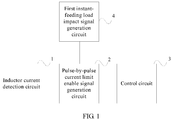
- FIG. 1 is a schematic structural diagram of Embodiment 1 of an overcurrent protection system for an inverter circuit according to the present invention.
- the overcurrent protection system for the inverter circuit in this embodiment may include: an inductor current detection circuit 1, a pulse-by-pulse current limit enable signal generation circuit 2, a control circuit 3, and a first instant-feeding load impact signal generation circuit 4.
- the inductor current detection circuit 1 is connected to the pulse-by-pulse current limit enable signal generation circuit 2
- the pulse-by-pulse current limit enable signal generation circuit 2 is connected to the control circuit 3
- the first instant-feeding load impact signal generation circuit 4 is connected to the pulse-by-pulse current limit enable signal generation circuit 2.
- the inductor current detection circuit 1 is configured to detect an inductor current in the inverter circuit, to obtain an inductor current detection value.
- the pulse-by-pulse current limit enable signal generation circuit 2 is configured to: reduce a current limit threshold according to an instant-feeding load impact signal; compare a current limit threshold obtained after reduction processing with a voltage value corresponding to the inductor current detection value; and if it is determined that the voltage value corresponding to the inductor current detection value reaches the current limit threshold, output a pulse-by-pulse current limit enable signal.
- the control circuit 3 is configured to perform turn-off control on a switching transistor in the inverter circuit according to the pulse-by-pulse current limit enable signal.
- turn-on or turn-off of the switching transistor is controlled according to the pulse-by-pulse current limit enable signal by using a pPulse Width Modulation (PWM) principle. That is, the control circuit 3 performs turn-off control on the switching transistor according to the pulse-by-pulse current limit enable signal when the pulse-by-pulse current limit enable signal generation circuit 2 outputs the pulse-by-pulse current limit enable signal if the voltage value corresponding to the inductor current detection value reaches the current limit threshold; or the control circuit 3 resumes normal on-off control on the switching transistor if the voltage value corresponding to the inductor current detection value does not reach the current limit threshold.
- PWM pPulse Width Modulation
- the first instant-feeding load impact signal generation circuit 4 is configured to: detect an inductor voltage in the inverter circuit, to obtain an inductor voltage detection value; and if it is determined that the inductor voltage detection value reaches a preset voltage threshold, generate the instant-feeding load impact signal.
- the instant-feeding load impact signal may be a pulse signal.
- the pulse-by-pulse current limit enable signal generation circuit 2 may reduce the current limit threshold according to the pulse signal.
- a specific implementation manner for implementing current limiting protection for the inverter circuit by using the foregoing overcurrent protection system for the inverter circuit may be as follows:
- the first instant-feeding load impact signal generation circuit 4 detects the inductor voltage in the inverter circuit, to obtain the inductor voltage detection value; compares the inductor voltage detection value with the preset voltage threshold; and when the inductor voltage detection value is greater than or equal to the preset voltage threshold, generates the instant-feeding load impact signal.
- the pulse-by-pulse current limit enable signal generation circuit 2 reduces the current limit threshold according to the instant-feeding load impact signal; compares the current limit threshold obtained after reduction processing with the voltage value corresponding to the inductor current detection value obtained by the inductor current detection circuit 1; and if the voltage value corresponding to the inductor current detection value reaches the current limit threshold, outputs the pulse-by-pulse current limit enable signal to the control circuit 3.
- the control circuit turns off the switching transistor in the inverter circuit according to the pulse-by-pulse current limit enable signal.
- the instant-feeding load impact signal is generated according to a comparison result of the voltage between the two ends of the inductor and the preset voltage threshold.
- the pulse-by-pulse current limit enable signal generation circuit reduces the current limit threshold, and outputs the pulse-by-pulse current limit enable signal according to the reduced current limit threshold.
- the control circuit performs turn-off control on the switching transistor according to the pulse-by-pulse current limit enable signal, so that current limiting protection for the switching transistor is implemented in advance by reducing the current limit threshold.
- the following problem is alleviated: Due to a circuit limitation, during a current limiting protection operation performed for the switching transistor when it is detected that the inductor current is greater than an overcurrent protection reference current, a delay ⁇ t cannot be eliminated before the current limiting protection operation takes effect.
- the current limiting protection operation takes effect before the inductor current is greater than the overcurrent protection reference current, thereby preventing damage to the switching transistor that is caused by overcurrent when the switching transistor is actually turned off.
- the overcurrent protection system for the inverter circuit is used to implement current limiting protection for the switching transistor, and has high reliability.
- FIG. 2 is a schematic structural diagram of Embodiment 2 of an overcurrent protection system for an inverter circuit according to the present invention.
- the overcurrent protection system for the inverter circuit in this embodiment is based on Embodiment 1.
- the first instant-feeding load impact signal generation circuit 4 may specifically include a voltage detection circuit 41 and a first load impact enable signal generation circuit 42.
- the control circuit 3 may specifically include a level conversion circuit 31 and a pulse-by-pulse current-limited circuit 32.
- the voltage detection circuit 41 acts on two ends of an inductor in the inverter circuit, and is configured to detect an inductor voltage in the inverter circuit, to obtain an inductor voltage detection value.
- the first load impact enable signal generation circuit 42 is separately connected to the voltage detection circuit 41 and the pulse-by-pulse current limit enable signal generation circuit 2, and is configured to: compare the inductor voltage detection value with a preset voltage threshold; and if it is determined that the inductor voltage detection value reaches the preset voltage threshold, generate an instant-feeding load impact signal.
- the level conversion circuit 31 is connected to the pulse-by-pulse current limit enable signal generation circuit 2, and is configured to perform level conversion on a pulse-by-pulse current limit enable signal, to obtain an overcurrent logic signal.
- the pulse-by-pulse current-limited circuit 32 is connected to the level conversion circuit 31, and is configured to perform turn-off control on a switching transistor in the inverter circuit according to the overcurrent logic signal.
- a specific implementation manner for implementing current limiting protection for the inverter circuit by using the foregoing overcurrent protection system for the inverter circuit is as follows:
- the voltage detection circuit 41 detects the inductor voltage in the inverter circuit, to obtain the inductor voltage detection value.
- the first load impact enable signal generation circuit 42 compares the inductor voltage detection value with the preset voltage threshold; and if it is determined that the inductor voltage detection value is greater than or equal to the preset voltage threshold, generates the instant-feeding load impact signal.
- the pulse-by-pulse current limit enable signal generation circuit 2 reduces a current limit threshold according to the instant-feeding load impact signal; compares a current limit threshold obtained after reduction processing with a voltage value corresponding to an inductor current detection value obtained by the inductor current detection circuit 1; and if the voltage value corresponding to the inductor current detection value reaches the current limit threshold, outputs the pulse-by-pulse current limit enable signal to the level conversion circuit 31.
- the level conversion circuit 31 performs level conversion on the pulse-by-pulse current limit enable signal, to obtain the overcurrent logic signal; and outputs the overcurrent logic signal to the pulse-by-pulse current-limited circuit 32.
- the pulse-by-pulse current-limited circuit 32 performs turn-off control on the switching transistor in the inverter circuit according to the overcurrent logic signal.
- a characteristic that the inductor voltage is ahead of the inductor current is used.
- the instant-feeding load impact signal is generated; and the current limit threshold for comparison with the inductor current detection value is reduced according to the instant-feeding load impact signal, so that current limiting protection can be implemented in advance, and timeliness of current limit can be ensured, thereby preventing damage to the switching transistor that is caused by overcurrent when the switching transistor is actually turned off.
- the current limit threshold may be gradually resumed to an initial state, so that a steady-state loading capability of the inverter circuit may not be affected.
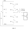
- FIG. 3 is a schematic diagram of a topology structure of a tri-level inverter circuit.
- FIG. 4 is a schematic diagram of waveforms of an inductor voltage and a current limit threshold in an inverter circuit. The foregoing overcurrent protection system for the inverter circuit is applied to the inverter circuit shown in FIG. 3 .
- L is an inductor in the inverter circuit
- Q1, Q2, Q3, and Q4 are switching transistors in the inverter circuit
- load represents a load
- C is an output capacitor.
- the output capacitor C When the foregoing inverter circuit is connected to a non-linear load, that is, when load is a non-linear load, the output capacitor C performs electric discharging on the load, causing a voltage U L between two ends of the inductor L to increase rapidly.
- the voltage detection circuit 41 in the overcurrent protection system for the inverter circuit obtains the voltage value U L between the two ends of the inductor. As shown in FIG. 4 , U L begins to increase rapidly from a time point 0. U L reaches U L _ REF at a time point t 0 , keeps U L _ REF from the time point to to a time point t 1 , and is smaller than U L_REF after the time point t 1 .
- the first load impact enable signal generation circuit 42 generates an instant-feeding load impact signal U L_OC .
- a waveform diagram of the instant-feeding load impact signal U L_OC is shown in FIG. 4 .
- a low level of U L_OC is set to active, and an active instant-feeding load impact signal is generated between the time point to and the time point t 1 .
- the pulse-by-pulse current limit enable signal generation circuit 2 reduces a current limit threshold V REF according to the instant-feeding load impact signal.
- an initial current limit threshold is V REF_ 0 .
- the pulse-by-pulse current limit enable signal generation circuit 2 reduces V REF_ 0 , to reduce the current limit threshold to V REF _ 0 ′ in a relatively short time; compares a voltage value corresponding to an inductor current detection value I L obtained by the inductor current detection circuit 1 with V REF _ 0 ′ ; and if the voltage value corresponding to the inductor current detection value I L is greater than or equal to V REF _ 0 ′ , outputs a pulse-by-pulse current limit enable signal.
- the level conversion circuit 31 performs level conversion on the pulse-by-pulse current limit enable signal, to obtain an overcurrent logic signal.
- the pulse-by-pulse current-limited circuit performs turn-off control on the switching transistor in the inverter circuit according to the overcurrent logic signal. It can be learnt from the schematic diagram of the waveform of the current limit threshold shown in FIG. 4 that, after the time point t 1 , the instant-feeding load impact signal becomes inactive; therefore, the current limit threshold V REF is gradually resumed to the initial current limit threshold V REF_ 0 , so that a steady-state loading capability of the inverter circuit may not be affected.
- FIG. 5 is a schematic structural diagram of Embodiment 3 of an overcurrent protection system for an inverter circuit according to the present invention.
- the overcurrent protection system may further include a second instant-feeding load impact signal generation circuit 5 and a selection circuit 6.
- the second instant-feeding load impact signal generation circuit 5 is connected to the pulse-by-pulse current limit enable signal generation circuit 2, and is configured to: detect an output current in the inverter circuit, to obtain an output-current detection value; and if it is determined that the output-current detection value reaches a preset current threshold, generate an instant-feeding load impact signal, that is, generate the instant-feeding load impact signal according to the output-current detection value.
- the output current in the inverter circuit is ahead of the inductor current; therefore, the instant-feeding load impact signal may be generated after a detection of the output current, so that current limiting protection is performed on a switching transistor in the inverter circuit in advance.
- the selection circuit 6 is separately connected to the first instant-feeding load impact signal generation circuit 4, the second instant-feeding load impact signal generation circuit 5, and the pulse-by-pulse current limit enable signal generation circuit 2, and is configured to select the instant-feeding load impact signal generated by the first instant-feeding load impact signal generation circuit 4 or the second instant-feeding load impact signal generation circuit 5 to be output to the pulse-by-pulse current limit enable signal generation circuit 2.
- instant-feeding load impact signal to be output to the pulse-by-pulse current limit enable signal generation circuit 2, provided that instant-feeding load impact information includes the instant-feeding load impact signal that is generated by the first instant-feeding load impact signal generation circuit 4 according to the inductor voltage and/or the instant-feeding load impact signal that is generated by the second instant-feeding load impact signal generation circuit 5 according to the output current.
- the second instant-feeding load impact signal generation circuit 5 may specifically include: a current detection circuit 51, configured to detect the output current in the inverter circuit, to obtain the output-current detection value; and a second load impact enable signal generation circuit 52, separately connected to the current detection circuit 51 and the pulse-by-pulse current limit enable signal generation circuit 2, and configured to: compare the output-current detection value with the preset current threshold; and if it is determined that the output-current detection value reaches the preset current threshold, generate the instant-feeding load impact signal.
- a current detection circuit 51 configured to detect the output current in the inverter circuit, to obtain the output-current detection value
- a second load impact enable signal generation circuit 52 separately connected to the current detection circuit 51 and the pulse-by-pulse current limit enable signal generation circuit 2, and configured to: compare the output-current detection value with the preset current threshold; and if it is determined that the output-current detection value reaches the preset current threshold, generate the instant-feeding load impact signal.
- a second instant-feeding load impact signal generation circuit 5 and a selection circuit 6 are added, so that an instant-feeding load impact signal can be generated according to an inductor voltage detection value, or an instant-feeding load impact signal can be generated according to an output current.
- a pulse-by-pulse current limit enable signal generation circuit 2 reduces a current limit threshold according to the instant-feeding load impact signal; compares a current limit threshold obtained after reduction processing with a voltage corresponding to an inductor current detection value; and when the voltage value corresponding to the inductor current detection value reaches the current limit threshold obtained after reduction processing, outputs a pulse-by-pulse current limit enable signal.
- a control circuit 3 performs turn-off control on a switching transistor in the inverter circuit according to the pulse-by-pulse current limit enable signal, so that current limiting protection for the switching transistor can be implemented in advance, and timeliness of current limit can be ensured, thereby preventing damage to the switching transistor that is caused by overcurrent when the switching transistor is actually turned off.
- the overcurrent protection system for the inverter circuit has high reliability.
- FIG. 6 is a schematic structural diagram an implementation example of an overcurrent protection system for an inverter circuit.
- the overcurrent protection system for the inverter circuit in this embodiment may include a first current-limited circuit and a second current-limited circuit.
- the first current-limited circuit is connected to the second current-limited circuit and a pulse-by-pulse current-limited circuit.
- the first current-limited circuit may include an inductor current detection circuit, a first pulse-by-pulse current limit enable signal generation circuit, and a first level conversion circuit.
- the inductor current detection circuit is configured to detect an inductor current in the inverter circuit, to obtain an inductor current detection value.
- the first pulse-by-pulse current limit enable signal generation circuit is configured to: compare a first preset current limit threshold with a voltage value corresponding to the inductor current detection value, where the first preset current limit threshold is a fixed reference voltage; and if it is determined that the voltage value corresponding to the inductor current detection value reaches the first preset current limit threshold, output a pulse-by-pulse current limit enable signal.
- the first level conversion circuit is configured to perform level conversion on the pulse-by-pulse current limit enable signal, to obtain a first overcurrent logic signal.
- the second current-limited circuit may include an inductor voltage detection circuit, a second pulse-by-pulse current limit enable signal generation circuit, and a second level conversion circuit.
- the inductor voltage detection circuit is configured to detect an inductor voltage in the inverter circuit, to obtain an inductor voltage detection value.
- the second pulse-by-pulse current limit enable signal generation circuit is configured to: compare a second preset current limit threshold with the inductor voltage detection value, where the second preset current limit threshold is a fixed reference voltage; and if it is determined that the inductor voltage detection value reaches the second preset current limit threshold, output a pulse-by-pulse current limit enable signal.
- the second level conversion circuit is configured to perform level conversion on the pulse-by-pulse current limit enable signal, to obtain a second overcurrent logic signal.
- the pulse-by-pulse current-limited circuit performs turn-off control on a switching transistor in the inverter circuit according to an overcurrent logic signal that is generated after an OR logical operation is performed between the first overcurrent logic signal and the second overcurrent logic signal.
- the OR logical operation performed between the first overcurrent logic signal and the second overcurrent logic signal may specifically be implemented by means of a software operation. Certainly, it may be understood that, a corresponding OR logical operation circuit may alternatively be disposed to perform the OR operation between the two overcurrent logic signals.
- two current-limited circuits are used to implement overcurrent protection for the inverter circuit.
- an inductor current is detected for protection: When the inductor current reaches a specified threshold, an inverter enters an overcurrent protection state; otherwise, the inverter works normally.
- a voltage between two ends of an inductor is used for protection: When the voltage between the two ends of the inductor abruptly changes to a specified threshold, the inverter enters an overcurrent protection state; otherwise, the inverter works normally.
- the inductor voltage in the inverter circuit is detected, and the inductor voltage detection value is compared with the preset voltage value.
- the pulse-by-pulse current limit enable signal is generated.
- OR logic may be implemented by the OR logic circuit, or may be implemented by determining by means of software, that is, a controller is used to detect output values of the two current-limited circuits.
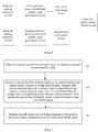
- FIG. 7 is a flowchart of Embodiment 1 of an overcurrent protection method for an inverter circuit according to the present invention. As shown in FIG. 7 , the method in this embodiment may include: Step 101: Detect an inductor current in the inverter circuit, to obtain an inductor current detection value.
- Step 102 Reduce a current limit threshold according to an instant-feeding load impact signal; compare a current limit threshold obtained after reduction processing with a voltage value corresponding to the inductor current detection value; and if it is determined that the voltage value corresponding to the inductor current detection value reaches the current limit threshold, output a pulse-by-pulse current limit enable signal.
- An inductor voltage in the inverter circuit is detected, to obtain an inductor voltage detection value; and if it is determined that the inductor voltage detection value reaches a preset voltage threshold, the instant-feeding load impact signal is generated. Reduction processing is performed on the current limit threshold after the instant-feeding load impact signal is generated according to the inductor voltage detection value.
- Step 103 Perform turn-off control on a switching transistor in the inverter circuit according to the pulse-by-pulse current limit enable signal.
- the performing turn-off control on a switching transistor in the inverter circuit according to the pulse-by-pulse current limit enable signal may specifically be: performing level conversion on the pulse-by-pulse current limit enable signal, to obtain an overcurrent logic signal; and performing turn-off control on the switching transistor in the inverter circuit according to the overcurrent logic signal.
- the foregoing instant-feeding load impact signal may further be obtained in the following manner: detecting an output current in the inverter circuit, to obtain an output-current detection value; and if it is determined that the output-current detection value reaches a preset current threshold, generating the instant-feeding load impact signal.
- an instant-feeding load impact signal is generated according to an inductor voltage detection value, and specifically, when the inductor voltage detection value reaches a preset voltage threshold, the instant-feeding load impact signal is generated; a current limit threshold is reduced according to the instant-feeding load impact signal; the reduced current limit threshold is compared with a voltage value corresponding to an inductor current detection value in an inverter circuit; when a voltage value corresponding to the inductor current detection value reaches the reduced current limit threshold, a pulse-by-pulse current limit enable signal is output; and turn-off control is performed on a switching transistor in the inverter circuit according to the pulse-by-pulse current limit enable signal, so that current limiting protection for the switching transistor is implemented in advance by reducing the current limit threshold according to an inductor voltage.
- a current limiting protection operation takes effect before an inductor current is greater than an overcurrent protection reference current, thereby preventing damage to the switching transistor that is caused by overcurrent when the switching transistor is actually turned off.
- the overcurrent protection method for the inverter circuit is used to implement current limiting protection for the switching transistor, and has high reliability.
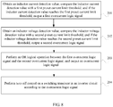
- FIG. 8 is a flowchart of an implementation example of an overcurrent protection method for an inverter circuit.
- the method in this embodiment may include: Step 201: Obtain an inductor current detection value; compare the inductor current detection value with a first preset current limit threshold; and if the inductor current detection value reaches the first preset current limit threshold, output a first overcurrent logic signal.
- step 201 may specifically be: detecting an inductor current in the inverter circuit, to obtain the inductor current detection value; comparing a voltage value corresponding to the inductor current detection value with the first preset current limit threshold; if it is determined that the voltage value corresponding to the inductor current detection value reaches the first preset current limit threshold, generating a first pulse-by-pulse current limit enable signal; and performing level conversion on the first pulse-by-pulse current limit enable signal, and outputting the first overcurrent logic signal.
- Step 202 Obtain an inductor voltage detection value; compare the inductor voltage detection value with a second preset current limit threshold; and if the inductor voltage detection value reaches the second preset current limit threshold, output a second overcurrent logic signal.
- step 202 may specifically be: detecting an inductor voltage in the inverter circuit, to obtain the inductor voltage detection value; comparing the inductor voltage detection value with the second preset current limit threshold; if it is determined that the inductor voltage detection value reaches the second preset current limit threshold, generating a second pulse-by-pulse current limit enable signal; and performing level conversion on the second pulse-by-pulse current limit enable signal, and outputting the second overcurrent logic signal.
- Step 203 Perform an OR logical operation between the first overcurrent logic signal and the second overcurrent logic signal, and output an overcurrent logic signal.
- Step 204 Perform turn-off control on a switching transistor in an inverter circuit according to the overcurrent logic signal.
- an inductor voltage in an inverter circuit is detected; an inductor voltage detection value is compared with a preset current limit threshold; when the inductor voltage detection value is greater than or equal to the preset current limit threshold, a second pulse-by-pulse current limit enable signal is generated; and level conversion is performed on the second pulse-by-pulse current limit enable signal to generate a second overcurrent logic signal.
- an inductor current in the inverter circuit is detected; a voltage corresponding to an inductor current detection value is compared with a preset current limit threshold; when the inductor current detection value is greater than or equal to the preset current limit threshold, a first pulse-by-pulse current limit enable signal; level conversion is performed on the first pulse-by-pulse current limit enable signal to generate a first overcurrent logic signal; and an OR operation is performed between the second overcurrent logic signal that is generated according to the inductor voltage detection value and the first overcurrent logic signal that is generated according to the inductor current detection value.
- an overcurrent logic signal is generated according to either the inductor voltage or the inductor current, so that there is an overcurrent logic signal for performing turn-off control on a switching transistor in the inverter circuit.
- current limiting protection for the switching transistor may be implemented in advance in this embodiment.
- the voltage between two ends of an inductor is not greater than a preset threshold, the current passing through the two ends of the inductor also reaches a relatively high current value as long as there is enough time. Therefore, in this embodiment, current limiting protection for the switching transistor in the inverter circuit is further implemented by detecting the inductor current in the inverter circuit.
- the overcurrent protection method for the inverter circuit in this embodiment has high reliability.
- the program may be stored in a computer-readable storage medium.
- the foregoing storage medium includes: any medium that can store program code, such as a ROM, a RAM, a magnetic disk, or an optical disc.
Landscapes
- Engineering & Computer Science (AREA)
- Power Engineering (AREA)
- Inverter Devices (AREA)
- Protection Of Static Devices (AREA)
Claims (6)
- Überstromschutzsystem für eine Wandlerschaltung, das Folgendes umfasst:eine Induktorstromdetektionsschaltung (1), die dazu ausgelegt ist, einen Induktorstrom, der einen Induktor in der Wandlerschaltung durchläuft, zu detektieren, um einen Induktorstromdetektionswert zu erhalten;eine Erzeugungsschaltung (2) für Impuls-für-Impuls-Stromgrenzwertaktivierungssignale, die mit der Induktorstromdetektionsschaltung verbunden und zu Folgendem ausgelegt ist: Reduzieren einer Stromgrenzwertschwelle gemäß einem momentanen Einspeisungslaststoßsignal;Vergleichen einer Stromgrenzwertschwelle, die nach der Reduktionsverarbeitung erhalten wird, mit einem Spannungswert, der dem Induktorstromdetektionswert entspricht; und Ausgeben eines Impuls-für-Impuls-Stromgrenzwertaktivierungssignals, wenn der Spannungswert, der dem Induktorstromdetektionswert entspricht, die Stromgrenzwertschwelle erreicht;eine Steuerschaltung (3), die mit der Erzeugungsschaltung für Impuls-für-Impuls-Stromgrenzwertaktivierungssignale verbunden und dazu ausgelegt ist, eine Abschaltsteuerung an einem Schalttransistor in der Wandlerschaltung gemäß dem Impuls-für-Impuls-Stromgrenzwertaktivierungssignal durchzuführen;gekennzeichnet durch:
eine erste Erzeugungsschaltung (4) für momentane Einspeisungslaststoßsignale, die mit der Erzeugungsschaltung für Impuls-für-Impuls-Stromgrenzwertaktivierungssignale verbunden und zu Folgendem ausgelegt ist: Detektieren einer Induktorspannung zwischen zwei Enden des Induktors in der Wandlerschaltung, um einen Induktorspannungsdetektionswert zu erhalten; und Erzeugen des momentanen Einspeisungslaststoßsignals, wenn der Induktorspannungsdetektionswert eine voreingestellte Spannungsschwelle erreicht. - System nach Anspruch 1, wobei die Steuerschaltung (3) Folgendes umfasst:eine Pegelumwandlungsschaltung (31), die mit der Erzeugungsschaltung für Impuls-für-Impuls-Stromgrenzwertaktivierungssignale verbunden und dazu ausgelegt ist, eine Pegelumwandlung am Impuls-für-Impuls-Stromgrenzwertaktivierungssignal durchzuführen, um ein Überstromlogiksignal zu erhalten; undeine strombegrenzte Impuls-für-Impuls-Schaltung (32), die mit der Pegelumwandlungsschaltung verbunden und dazu ausgelegt ist, gemäß dem Überstromlogiksignal eine Abschaltsteuerung am Schalttransistor in der Wandlerschaltung durchzuführen.
- System nach einem der Ansprüche 1 bis 2, das ferner Folgendes umfasst:
eine zweite Erzeugungsschaltung (5) für momentane Einspeisungslaststoßsignale, die mit der Erzeugungsschaltung für Impuls-für-Impuls-Stromgrenzwertaktivierungssignale verbunden und zu Folgendem ausgelegt ist:Detektieren eines Ausgangsstroms in der Wandlerschaltung, um einen Ausgangsstromdetektionswert zu erhalten; und wenn bestimmt wird, dass der Ausgangsstromdetektionswert eine voreingestellte Stromschwelle erreicht, Erzeugen des momentanen Einspeisungslaststoßsignals; undeine Auswahlschaltung (6), die mit der ersten Erzeugungsschaltung für momentane Einspeisungslaststoßsignale, der zweiten Erzeugungsschaltung für momentane Einspeisungslaststoßsignale und der Erzeugungsschaltung für Impuls-für-Impuls-Stromgrenzwertaktivierungssignale separat verbunden und dazu ausgelegt ist, das momentane Einspeisungslaststoßsignal, das von der ersten Erzeugungsschaltung für momentane Einspeisungslaststoßsignale oder von der zweiten Erzeugungsschaltung für momentane Einspeisungslaststoßsignale erzeugt wird und zur Erzeugungsschaltung für Impuls-für-Impuls-Stromgrenzwertaktivierungssignale auszugeben ist, auszuwählen. - Überstromschutzverfahren für eine Wandlerschaltung, das Folgendes umfasst:Detektieren (101) eines Induktorstroms, der einen Induktor in der Wandlerschaltung durchläuft, um einen Induktorstromdetektionswert zu erhalten;Reduzieren (102) einer Stromgrenzwertschwelle gemäß einem momentanen Einspeisungslaststoßsignal; Vergleichen einer Stromgrenzwertschwelle, die nach der Reduktionsverarbeitung erhalten wird, mit einem Spannungswert, der dem Induktorstromdetektionswert entspricht; und, wenn bestimmt wird, dass der Spannungswert, der dem Induktorstromdetektionswert entspricht, die Stromgrenzwertschwelle erreicht, Ausgeben eines Impuls-für-Impuls-Stromgrenzwertaktivierungssignals;Durchführen (103) einer Abschaltsteuerung an einem Schalttransistor in der Wandlerschaltung gemäß dem Impuls-für-Impuls-Stromgrenzwertaktivierungssignal;gekennzeichnet durchDetektieren einer Induktorspannung zwischen zwei Enden des Induktors in der Wandlerschaltung, um einen Induktorspannungsdetektionswert zu erhalten; und,wenn bestimmt wird, dass der Induktorspannungsdetektionswert eine voreingestellte Spannungsschwelle erreicht, Erzeugen des momentanen Einspeisungslaststoßsignals.
- Verfahren nach Anspruch 4, wobei das Durchführen einer Abschaltsteuerung an einem Schalttransistor in der Wandlerschaltung gemäß dem Impuls-für-Impuls-Stromgrenzwertaktivierungssignal Folgendes umfasst:Durchführen einer Pegelumwandlung am Impuls-für-Impuls-Stromgrenzwertaktivierungssignal, um ein Überstromlogiksignal zu erhalten; undDurchführen einer Abschaltsteuerung am Schalttransistor in der Wandlerschaltung gemäß dem Überstromlogiksignal.
- Verfahren nach Anspruch 4 oder 5, wobei das momentane Einspeisungslaststoßsignal von einer ersten Erzeugungsschaltung (4) für momentane Einspeisungslaststoßsignale erzeugt wird, wobei das Verfahren ferner Folgendes umfasst:Detektieren eines Ausgangsstroms in der Wandlerschaltung, um einen Ausgangsstromdetektionswert zu erhalten; und wenn bestimmt wird, dass der Ausgangsstromdetektionswert eine voreingestellte Stromschwelle erreicht, Erzeugen des momentanen Einspeisungslaststoßsignals durch eine zweite Erzeugungsschaltung (5) für momentane Einspeisungslaststoßsignale undAuswählen des momentanen Einspeisungslaststoßsignals, das von der ersten Erzeugungsschaltung (4) für momentane Einspeisungslaststoßsignale oder von der zweiten Erzeugungsschaltung (5) für momentane Einspeisungslaststoßsignale erzeugt wird und zur Erzeugungsschaltung für Impuls-für-Impuls-Stromgrenzwertaktivierungssignale auszugeben ist, durch eine Auswahlschaltung (6).
Applications Claiming Priority (2)
| Application Number | Priority Date | Filing Date | Title |
|---|---|---|---|
| CN201410360242.1A CN104104062B (zh) | 2014-07-25 | 2014-07-25 | 逆变器电路的过流保护系统和方法 |
| PCT/CN2015/083598 WO2016011893A1 (zh) | 2014-07-25 | 2015-07-08 | 逆变器电路的过流保护系统和方法 |
Publications (3)
| Publication Number | Publication Date |
|---|---|
| EP3163702A1 EP3163702A1 (de) | 2017-05-03 |
| EP3163702A4 EP3163702A4 (de) | 2017-11-29 |
| EP3163702B1 true EP3163702B1 (de) | 2020-09-02 |
Family
ID=51671979
Family Applications (1)
| Application Number | Title | Priority Date | Filing Date |
|---|---|---|---|
| EP15824464.0A Active EP3163702B1 (de) | 2014-07-25 | 2015-07-08 | Überstromschutzsystem und -verfahren für wechselrichterschaltung |
Country Status (4)
| Country | Link |
|---|---|
| US (1) | US9906120B2 (de) |
| EP (1) | EP3163702B1 (de) |
| CN (1) | CN104104062B (de) |
| WO (1) | WO2016011893A1 (de) |
Families Citing this family (13)
| Publication number | Priority date | Publication date | Assignee | Title |
|---|---|---|---|---|
| CN104104062B (zh) * | 2014-07-25 | 2018-01-16 | 华为技术有限公司 | 逆变器电路的过流保护系统和方法 |
| CN107612302B (zh) * | 2017-11-09 | 2020-05-26 | 深圳市英威腾光伏科技有限公司 | 一种逆变器限流保护方法及系统 |
| CN109873556B (zh) * | 2017-12-01 | 2020-03-17 | 维谛技术有限公司 | 一种三电平逆变器的限流控制方法和装置 |
| CN110926798A (zh) * | 2019-12-25 | 2020-03-27 | 北京航天测控技术有限公司 | 一种电磁阀开关状态判定方法及装置 |
| CN112072616B (zh) * | 2020-09-02 | 2021-09-14 | 珠海格力电器股份有限公司 | Ipm过流检测电路及电器 |
| CN113346452B (zh) * | 2021-05-17 | 2022-10-14 | 珠海格力电器股份有限公司 | 一种过流保护装置、磁悬浮系统及其过流保护方法 |
| CN114421750A (zh) * | 2021-12-30 | 2022-04-29 | 深圳市禾望科技有限公司 | 一种逆变器功率开关管动态保护控制方法 |
| CN115242072B (zh) * | 2022-09-16 | 2022-12-23 | 深圳市首航新能源股份有限公司 | 一种降低逆变管应力的方法、装置及逆变器 |
| CN115296272B (zh) * | 2022-10-08 | 2023-01-06 | 美世乐(广东)新能源科技有限公司 | 一种逆变器的过流保护方法 |
| CN115498692A (zh) * | 2022-10-13 | 2022-12-20 | 阳光电源股份有限公司 | 新能源发电系统、风电变流器、光伏逆变器、电压源型交直流变换器及其低压穿越方法 |
| CN115441413B (zh) * | 2022-11-09 | 2023-03-03 | 浙江日风电气股份有限公司 | 一种逐波限流控制方法及相关组件 |
| CN116111824B (zh) * | 2023-03-06 | 2025-04-11 | 苏州贝瓦科技有限公司 | 用于三电平电路的控制方法及其装置 |
| CN116885937B (zh) * | 2023-09-04 | 2023-12-08 | 西安千帆翼数字能源技术有限公司 | 一种三相四桥臂逆变器逐波限流方法及系统 |
Family Cites Families (11)
| Publication number | Priority date | Publication date | Assignee | Title |
|---|---|---|---|---|
| US7466039B2 (en) * | 2006-09-18 | 2008-12-16 | Linear Technology Corporation | Reducing oscillations in system with foldback current limit when inductive load is connected |
| CN102624273B (zh) | 2012-04-27 | 2014-10-08 | 华为技术有限公司 | 逆变器限流控制方法和装置 |
| CN102694479B (zh) | 2012-05-25 | 2015-04-08 | 华为技术有限公司 | 一种电力电子电路 |
| CN102739090B (zh) * | 2012-07-02 | 2014-06-25 | 华为技术有限公司 | 一种逆变器的过流保护装置及方法、逆变器 |
| CN102868291B (zh) * | 2012-09-19 | 2015-08-19 | 华为技术有限公司 | 二极管中点箝位型三电平逆变器限流控制方法及相关电路 |
| US20140253080A1 (en) * | 2013-03-11 | 2014-09-11 | Qualcomm Incorporated | Method and apparatus for advanced pulse skipping control in buck regulators |
| CN103280960B (zh) * | 2013-05-31 | 2015-04-15 | 华为技术有限公司 | 限流装置及限流方法 |
| CN203674694U (zh) * | 2013-10-11 | 2014-06-25 | 深圳市伟创电气有限公司 | 一种变频器的逐波限流保护电路 |
| CN105004910A (zh) * | 2014-04-22 | 2015-10-28 | 中兴通讯股份有限公司 | 一种pfc电感的电流检测方法及装置 |
| CN104104062B (zh) * | 2014-07-25 | 2018-01-16 | 华为技术有限公司 | 逆变器电路的过流保护系统和方法 |
| CN104660022B (zh) * | 2015-02-02 | 2017-06-13 | 昂宝电子(上海)有限公司 | 为电源变换器提供过流保护的系统和方法 |
-
2014
- 2014-07-25 CN CN201410360242.1A patent/CN104104062B/zh active Active
-
2015
- 2015-07-08 WO PCT/CN2015/083598 patent/WO2016011893A1/zh not_active Ceased
- 2015-07-08 EP EP15824464.0A patent/EP3163702B1/de active Active
-
2017
- 2017-01-24 US US15/414,375 patent/US9906120B2/en active Active
Non-Patent Citations (1)
| Title |
|---|
| None * |
Also Published As
| Publication number | Publication date |
|---|---|
| CN104104062B (zh) | 2018-01-16 |
| US9906120B2 (en) | 2018-02-27 |
| EP3163702A1 (de) | 2017-05-03 |
| EP3163702A4 (de) | 2017-11-29 |
| WO2016011893A1 (zh) | 2016-01-28 |
| CN104104062A (zh) | 2014-10-15 |
| US20170133925A1 (en) | 2017-05-11 |
Similar Documents
| Publication | Publication Date | Title |
|---|---|---|
| US9906120B2 (en) | Overcurrent protection system and method for inverter circuit | |
| US9825453B2 (en) | Protection mode control circuit, switch control circuit including the protection mode control circuit and power supply device including the switch control circuit | |
| US10236677B2 (en) | Semiconductor device | |
| US9923365B2 (en) | Short-circuit protection circuit for voltage sampling resistor of primary side converter | |
| EP2897270B1 (de) | Schaltkondensator-Gleichstromwandler mit verringerter Einschaltstrombegrenzung und Fehlerschutz | |
| US8811042B2 (en) | Systems and methods for protecting power conversion systems under open and/or short circuit conditions | |
| US8547676B2 (en) | Overcurrent protection device and overcurrent protection system | |
| US9083181B2 (en) | Over-current protection circuit for light source driving module and related backlight module | |
| CN106300944B (zh) | 过流控制电路、过流控制方法及应用其的电源系统 | |
| US20190115841A1 (en) | Switched-mode power supply circuit | |
| US9331474B1 (en) | Over-voltage protection circuit for a drive transistor | |
| US10176949B2 (en) | Control apparatus for relay and controlling method thereof | |
| KR20150075034A (ko) | 스위칭 레귤레이터 및 전자 기기 | |
| US9812941B2 (en) | High power driver having multiple turn off modes | |
| US10756626B2 (en) | Power conversion circuit | |
| CN112886541B (zh) | 一种变换器及igbt门极驱动的保护电路和方法 | |
| KR20160064004A (ko) | Dc-dc 컨버터 | |
| US9729043B2 (en) | Power conversion apparatus and protection method thereof while feedback current signal being abnormal | |
| GB2430502A (en) | Switching regulator with over-current protection | |
| US20170070224A1 (en) | Wave loss detection circuit for drive signal and switching transistor drive circuit | |
| JP6053235B2 (ja) | 電源装置 | |
| EP3174196A1 (de) | Fotovoltaiksystem | |
| CN108418187A (zh) | 一种功率变换电路及其驱动电路和输出短路保护方法 | |
| KR20180015367A (ko) | 펄스 전원 장치 스위칭 제어 회로 | |
| EP2629384A1 (de) | Schutzschaltung und Vorrichtung zum Schutz von elektrischen Vorrichtungen |
Legal Events
| Date | Code | Title | Description |
|---|---|---|---|
| STAA | Information on the status of an ep patent application or granted ep patent |
Free format text: STATUS: THE INTERNATIONAL PUBLICATION HAS BEEN MADE |
|
| PUAI | Public reference made under article 153(3) epc to a published international application that has entered the european phase |
Free format text: ORIGINAL CODE: 0009012 |
|
| STAA | Information on the status of an ep patent application or granted ep patent |
Free format text: STATUS: REQUEST FOR EXAMINATION WAS MADE |
|
| 17P | Request for examination filed |
Effective date: 20170127 |
|
| AK | Designated contracting states |
Kind code of ref document: A1 Designated state(s): AL AT BE BG CH CY CZ DE DK EE ES FI FR GB GR HR HU IE IS IT LI LT LU LV MC MK MT NL NO PL PT RO RS SE SI SK SM TR |
|
| AX | Request for extension of the european patent |
Extension state: BA ME |
|
| DAV | Request for validation of the european patent (deleted) | ||
| DAX | Request for extension of the european patent (deleted) | ||
| A4 | Supplementary search report drawn up and despatched |
Effective date: 20171027 |
|
| RIC1 | Information provided on ipc code assigned before grant |
Ipc: H02H 9/00 20060101ALI20171023BHEP Ipc: H02H 3/08 20060101ALN20171023BHEP Ipc: H02H 7/122 20060101AFI20171023BHEP |
|
| STAA | Information on the status of an ep patent application or granted ep patent |
Free format text: STATUS: EXAMINATION IS IN PROGRESS |
|
| 17Q | First examination report despatched |
Effective date: 20190716 |
|
| RIC1 | Information provided on ipc code assigned before grant |
Ipc: H02H 9/00 20060101ALI20200127BHEP Ipc: H02H 7/122 20060101AFI20200127BHEP Ipc: H02H 3/08 20060101ALN20200127BHEP |
|
| GRAP | Despatch of communication of intention to grant a patent |
Free format text: ORIGINAL CODE: EPIDOSNIGR1 |
|
| STAA | Information on the status of an ep patent application or granted ep patent |
Free format text: STATUS: GRANT OF PATENT IS INTENDED |
|
| INTG | Intention to grant announced |
Effective date: 20200310 |
|
| GRAS | Grant fee paid |
Free format text: ORIGINAL CODE: EPIDOSNIGR3 |
|
| GRAA | (expected) grant |
Free format text: ORIGINAL CODE: 0009210 |
|
| STAA | Information on the status of an ep patent application or granted ep patent |
Free format text: STATUS: THE PATENT HAS BEEN GRANTED |
|
| AK | Designated contracting states |
Kind code of ref document: B1 Designated state(s): AL AT BE BG CH CY CZ DE DK EE ES FI FR GB GR HR HU IE IS IT LI LT LU LV MC MK MT NL NO PL PT RO RS SE SI SK SM TR |
|
| REG | Reference to a national code |
Ref country code: GB Ref legal event code: FG4D |
|
| REG | Reference to a national code |
Ref country code: AT Ref legal event code: REF Ref document number: 1309916 Country of ref document: AT Kind code of ref document: T Effective date: 20200915 Ref country code: CH Ref legal event code: EP |
|
| REG | Reference to a national code |
Ref country code: DE Ref legal event code: R096 Ref document number: 602015058535 Country of ref document: DE |
|
| REG | Reference to a national code |
Ref country code: IE Ref legal event code: FG4D |
|
| REG | Reference to a national code |
Ref country code: LT Ref legal event code: MG4D |
|
| PG25 | Lapsed in a contracting state [announced via postgrant information from national office to epo] |
Ref country code: FI Free format text: LAPSE BECAUSE OF FAILURE TO SUBMIT A TRANSLATION OF THE DESCRIPTION OR TO PAY THE FEE WITHIN THE PRESCRIBED TIME-LIMIT Effective date: 20200902 Ref country code: HR Free format text: LAPSE BECAUSE OF FAILURE TO SUBMIT A TRANSLATION OF THE DESCRIPTION OR TO PAY THE FEE WITHIN THE PRESCRIBED TIME-LIMIT Effective date: 20200902 Ref country code: GR Free format text: LAPSE BECAUSE OF FAILURE TO SUBMIT A TRANSLATION OF THE DESCRIPTION OR TO PAY THE FEE WITHIN THE PRESCRIBED TIME-LIMIT Effective date: 20201203 Ref country code: NO Free format text: LAPSE BECAUSE OF FAILURE TO SUBMIT A TRANSLATION OF THE DESCRIPTION OR TO PAY THE FEE WITHIN THE PRESCRIBED TIME-LIMIT Effective date: 20201202 Ref country code: SE Free format text: LAPSE BECAUSE OF FAILURE TO SUBMIT A TRANSLATION OF THE DESCRIPTION OR TO PAY THE FEE WITHIN THE PRESCRIBED TIME-LIMIT Effective date: 20200902 Ref country code: BG Free format text: LAPSE BECAUSE OF FAILURE TO SUBMIT A TRANSLATION OF THE DESCRIPTION OR TO PAY THE FEE WITHIN THE PRESCRIBED TIME-LIMIT Effective date: 20201202 Ref country code: LT Free format text: LAPSE BECAUSE OF FAILURE TO SUBMIT A TRANSLATION OF THE DESCRIPTION OR TO PAY THE FEE WITHIN THE PRESCRIBED TIME-LIMIT Effective date: 20200902 |
|
| REG | Reference to a national code |
Ref country code: NL Ref legal event code: MP Effective date: 20200902 |
|
| REG | Reference to a national code |
Ref country code: AT Ref legal event code: MK05 Ref document number: 1309916 Country of ref document: AT Kind code of ref document: T Effective date: 20200902 |
|
| PG25 | Lapsed in a contracting state [announced via postgrant information from national office to epo] |
Ref country code: PL Free format text: LAPSE BECAUSE OF FAILURE TO SUBMIT A TRANSLATION OF THE DESCRIPTION OR TO PAY THE FEE WITHIN THE PRESCRIBED TIME-LIMIT Effective date: 20200902 Ref country code: RS Free format text: LAPSE BECAUSE OF FAILURE TO SUBMIT A TRANSLATION OF THE DESCRIPTION OR TO PAY THE FEE WITHIN THE PRESCRIBED TIME-LIMIT Effective date: 20200902 Ref country code: LV Free format text: LAPSE BECAUSE OF FAILURE TO SUBMIT A TRANSLATION OF THE DESCRIPTION OR TO PAY THE FEE WITHIN THE PRESCRIBED TIME-LIMIT Effective date: 20200902 |
|
| PG25 | Lapsed in a contracting state [announced via postgrant information from national office to epo] |
Ref country code: NL Free format text: LAPSE BECAUSE OF FAILURE TO SUBMIT A TRANSLATION OF THE DESCRIPTION OR TO PAY THE FEE WITHIN THE PRESCRIBED TIME-LIMIT Effective date: 20200902 Ref country code: SM Free format text: LAPSE BECAUSE OF FAILURE TO SUBMIT A TRANSLATION OF THE DESCRIPTION OR TO PAY THE FEE WITHIN THE PRESCRIBED TIME-LIMIT Effective date: 20200902 Ref country code: PT Free format text: LAPSE BECAUSE OF FAILURE TO SUBMIT A TRANSLATION OF THE DESCRIPTION OR TO PAY THE FEE WITHIN THE PRESCRIBED TIME-LIMIT Effective date: 20210104 Ref country code: RO Free format text: LAPSE BECAUSE OF FAILURE TO SUBMIT A TRANSLATION OF THE DESCRIPTION OR TO PAY THE FEE WITHIN THE PRESCRIBED TIME-LIMIT Effective date: 20200902 Ref country code: EE Free format text: LAPSE BECAUSE OF FAILURE TO SUBMIT A TRANSLATION OF THE DESCRIPTION OR TO PAY THE FEE WITHIN THE PRESCRIBED TIME-LIMIT Effective date: 20200902 Ref country code: CZ Free format text: LAPSE BECAUSE OF FAILURE TO SUBMIT A TRANSLATION OF THE DESCRIPTION OR TO PAY THE FEE WITHIN THE PRESCRIBED TIME-LIMIT Effective date: 20200902 |
|
| PG25 | Lapsed in a contracting state [announced via postgrant information from national office to epo] |
Ref country code: ES Free format text: LAPSE BECAUSE OF FAILURE TO SUBMIT A TRANSLATION OF THE DESCRIPTION OR TO PAY THE FEE WITHIN THE PRESCRIBED TIME-LIMIT Effective date: 20200902 Ref country code: AL Free format text: LAPSE BECAUSE OF FAILURE TO SUBMIT A TRANSLATION OF THE DESCRIPTION OR TO PAY THE FEE WITHIN THE PRESCRIBED TIME-LIMIT Effective date: 20200902 Ref country code: AT Free format text: LAPSE BECAUSE OF FAILURE TO SUBMIT A TRANSLATION OF THE DESCRIPTION OR TO PAY THE FEE WITHIN THE PRESCRIBED TIME-LIMIT Effective date: 20200902 Ref country code: IS Free format text: LAPSE BECAUSE OF FAILURE TO SUBMIT A TRANSLATION OF THE DESCRIPTION OR TO PAY THE FEE WITHIN THE PRESCRIBED TIME-LIMIT Effective date: 20210102 |
|
| REG | Reference to a national code |
Ref country code: DE Ref legal event code: R097 Ref document number: 602015058535 Country of ref document: DE |
|
| PG25 | Lapsed in a contracting state [announced via postgrant information from national office to epo] |
Ref country code: SK Free format text: LAPSE BECAUSE OF FAILURE TO SUBMIT A TRANSLATION OF THE DESCRIPTION OR TO PAY THE FEE WITHIN THE PRESCRIBED TIME-LIMIT Effective date: 20200902 |
|
| PLBE | No opposition filed within time limit |
Free format text: ORIGINAL CODE: 0009261 |
|
| STAA | Information on the status of an ep patent application or granted ep patent |
Free format text: STATUS: NO OPPOSITION FILED WITHIN TIME LIMIT |
|
| 26N | No opposition filed |
Effective date: 20210603 |
|
| PG25 | Lapsed in a contracting state [announced via postgrant information from national office to epo] |
Ref country code: DK Free format text: LAPSE BECAUSE OF FAILURE TO SUBMIT A TRANSLATION OF THE DESCRIPTION OR TO PAY THE FEE WITHIN THE PRESCRIBED TIME-LIMIT Effective date: 20200902 Ref country code: SI Free format text: LAPSE BECAUSE OF FAILURE TO SUBMIT A TRANSLATION OF THE DESCRIPTION OR TO PAY THE FEE WITHIN THE PRESCRIBED TIME-LIMIT Effective date: 20200902 |
|
| PG25 | Lapsed in a contracting state [announced via postgrant information from national office to epo] |
Ref country code: IT Free format text: LAPSE BECAUSE OF FAILURE TO SUBMIT A TRANSLATION OF THE DESCRIPTION OR TO PAY THE FEE WITHIN THE PRESCRIBED TIME-LIMIT Effective date: 20200902 |
|
| REG | Reference to a national code |
Ref country code: DE Ref legal event code: R081 Ref document number: 602015058535 Country of ref document: DE Owner name: HUAWEI DIGITAL POWER TECHNOLOGIES CO., LTD., S, CN Free format text: FORMER OWNER: HUAWEI TECHNOLOGIES CO., LTD., SHENZHEN, GUANGDONG, CN |
|
| REG | Reference to a national code |
Ref country code: CH Ref legal event code: PL |
|
| GBPC | Gb: european patent ceased through non-payment of renewal fee |
Effective date: 20210708 |
|
| PG25 | Lapsed in a contracting state [announced via postgrant information from national office to epo] |
Ref country code: MC Free format text: LAPSE BECAUSE OF FAILURE TO SUBMIT A TRANSLATION OF THE DESCRIPTION OR TO PAY THE FEE WITHIN THE PRESCRIBED TIME-LIMIT Effective date: 20200902 |
|
| REG | Reference to a national code |
Ref country code: BE Ref legal event code: MM Effective date: 20210731 |
|
| PG25 | Lapsed in a contracting state [announced via postgrant information from national office to epo] |
Ref country code: LI Free format text: LAPSE BECAUSE OF NON-PAYMENT OF DUE FEES Effective date: 20210731 Ref country code: GB Free format text: LAPSE BECAUSE OF NON-PAYMENT OF DUE FEES Effective date: 20210708 Ref country code: CH Free format text: LAPSE BECAUSE OF NON-PAYMENT OF DUE FEES Effective date: 20210731 |
|
| PG25 | Lapsed in a contracting state [announced via postgrant information from national office to epo] |
Ref country code: LU Free format text: LAPSE BECAUSE OF NON-PAYMENT OF DUE FEES Effective date: 20210708 Ref country code: FR Free format text: LAPSE BECAUSE OF NON-PAYMENT OF DUE FEES Effective date: 20210731 |
|
| PG25 | Lapsed in a contracting state [announced via postgrant information from national office to epo] |
Ref country code: IE Free format text: LAPSE BECAUSE OF NON-PAYMENT OF DUE FEES Effective date: 20210708 Ref country code: BE Free format text: LAPSE BECAUSE OF NON-PAYMENT OF DUE FEES Effective date: 20210731 |
|
| PG25 | Lapsed in a contracting state [announced via postgrant information from national office to epo] |
Ref country code: HU Free format text: LAPSE BECAUSE OF FAILURE TO SUBMIT A TRANSLATION OF THE DESCRIPTION OR TO PAY THE FEE WITHIN THE PRESCRIBED TIME-LIMIT; INVALID AB INITIO Effective date: 20150708 |
|
| PG25 | Lapsed in a contracting state [announced via postgrant information from national office to epo] |
Ref country code: CY Free format text: LAPSE BECAUSE OF FAILURE TO SUBMIT A TRANSLATION OF THE DESCRIPTION OR TO PAY THE FEE WITHIN THE PRESCRIBED TIME-LIMIT Effective date: 20200902 |
|
| PG25 | Lapsed in a contracting state [announced via postgrant information from national office to epo] |
Ref country code: MK Free format text: LAPSE BECAUSE OF FAILURE TO SUBMIT A TRANSLATION OF THE DESCRIPTION OR TO PAY THE FEE WITHIN THE PRESCRIBED TIME-LIMIT Effective date: 20200902 |
|
| PG25 | Lapsed in a contracting state [announced via postgrant information from national office to epo] |
Ref country code: MT Free format text: LAPSE BECAUSE OF FAILURE TO SUBMIT A TRANSLATION OF THE DESCRIPTION OR TO PAY THE FEE WITHIN THE PRESCRIBED TIME-LIMIT Effective date: 20200902 |
|
| P01 | Opt-out of the competence of the unified patent court (upc) registered |
Free format text: CASE NUMBER: UPC_APP_328938/2023 Effective date: 20230524 |
|
| PGFP | Annual fee paid to national office [announced via postgrant information from national office to epo] |
Ref country code: DE Payment date: 20250604 Year of fee payment: 11 |
|
| PG25 | Lapsed in a contracting state [announced via postgrant information from national office to epo] |
Ref country code: TR Free format text: LAPSE BECAUSE OF FAILURE TO SUBMIT A TRANSLATION OF THE DESCRIPTION OR TO PAY THE FEE WITHIN THE PRESCRIBED TIME-LIMIT Effective date: 20200902 |