EP3163580A1 - Method and device for compact efuse array - Google Patents
Method and device for compact efuse array Download PDFInfo
- Publication number
- EP3163580A1 EP3163580A1 EP16196134.7A EP16196134A EP3163580A1 EP 3163580 A1 EP3163580 A1 EP 3163580A1 EP 16196134 A EP16196134 A EP 16196134A EP 3163580 A1 EP3163580 A1 EP 3163580A1
- Authority
- EP
- European Patent Office
- Prior art keywords
- efuse
- coupled
- diode
- cell
- bit line
- Prior art date
- Legal status (The legal status is an assumption and is not a legal conclusion. Google has not performed a legal analysis and makes no representation as to the accuracy of the status listed.)
- Granted
Links
Images


Classifications
-
- G—PHYSICS
- G11—INFORMATION STORAGE
- G11C—STATIC STORES
- G11C17/00—Read-only memories programmable only once; Semi-permanent stores, e.g. manually-replaceable information cards
- G11C17/14—Read-only memories programmable only once; Semi-permanent stores, e.g. manually-replaceable information cards in which contents are determined by selectively establishing, breaking or modifying connecting links by permanently altering the state of coupling elements, e.g. PROM
- G11C17/18—Auxiliary circuits, e.g. for writing into memory
-
- G—PHYSICS
- G11—INFORMATION STORAGE
- G11C—STATIC STORES
- G11C17/00—Read-only memories programmable only once; Semi-permanent stores, e.g. manually-replaceable information cards
- G11C17/14—Read-only memories programmable only once; Semi-permanent stores, e.g. manually-replaceable information cards in which contents are determined by selectively establishing, breaking or modifying connecting links by permanently altering the state of coupling elements, e.g. PROM
- G11C17/16—Read-only memories programmable only once; Semi-permanent stores, e.g. manually-replaceable information cards in which contents are determined by selectively establishing, breaking or modifying connecting links by permanently altering the state of coupling elements, e.g. PROM using electrically-fusible links
Definitions
- the present invention relates to the field of semiconductor technology. Specifically, embodiments of the invention are directed to an electrically programmable fuse (eFuse) cell array and memory device.
- eFuse electrically programmable fuse
- An eFuse is an electrically programmable memory device whose resistance can be changed by passing an electric current through it. It usually can be programmed only one time. Programmed eFuses are electrically high resistance, while unprogrammed eFuses remain in a low resistance state.
- An eFuse can be implemented using different technologies. For example, an eFuse can be made of a conductive line, which can transition to a high resistance state or can be broken by applying a large current through it. In another example, an eFuse can be made of a polysilicon line coated with a silicide layer. The programming current can cause the silicide layer to redistribute and be broken, resulting in the high resistance state. In computing, an eFuse allows for the dynamic real-time reprogramming of computer chips. By utilizing eFuses, a chip manufacturer can allow for the circuits on a chip to be changed by applying an electrical signal.
- eFuse electrical programmable fuse
- all devices in the eFuse array are core devices.
- the operating voltage in the core devices is very low.
- the high voltage needed in programming or burning the eFuse can be a challenge.
- Some conventional methods have been proposed to overcome the high programming voltage eFuse array.
- an LDO Low dropout regulator
- this approach can result in a large area of the device.
- each eFise cell has an eFuse and an NMOS transistor connected in series.
- the NMOS can be HVNMOS (high voltage NMOS), in which the gate voltage is close to the programming voltage.
- HVNMOS high voltage NMOS
- the area of the HVNMOS area is larger than the core device, resulting in peripheral circuits of such eFuse array becoming relatively large. Therefore, the size of a low capacity eFuse array can be dominated by the LDO circuit, and the size of a high-capacity eFuse can be dominated by the eFuse cell size.
- the high voltage bit line operations in an eFuse array can adversely affect its reliability, e.g., the total number of operations.
- the peripheral devices which can include word line drivers, pass gate drivers, PMOS switches and drivers, as well as level converters, etc.
- the present invention relates to the field of semiconductor technology. Specifically, embodiments of the invention are directed to an electrical (programmable) fuse (eFuse) cell, a compact electrically programmable fuse (eFuse) cell array and a storage unit.
- eFuse electrical (programmable) fuse
- eFuse compact electrically programmable fuse
- an electrically (programmable) fuse (eFuse) cell includes first, second, and third terminals, an eFuse, a first diode, and a second diode.
- the eFuse, the first diode, and the second diode are coupled to an internal node.
- the first diode is coupled between the first terminal and the internal node
- the second diode is coupled between the second terminal and the internal node
- the eFuse is coupled between the third terminal and the internal node.
- Each eFuse cell may include a PNP bipolar transistor, in which the first diode is formed by a first PN junction of the bipolar transistor, the second diode is formed by a second PN junction of the bipolar transistor, and the internal node is a base of the bipolar transistor.
- an electrical (programmable) fuse (eFuse) cell may includes first, second, and third terminals, an eFuse, and a PNP bipolar transistor having a first P-type region, an N-type base region, and a second P-type region.
- the first terminal is coupled to the first P-type region
- the second terminal is coupled to the second P-type region
- the eFuse is coupled between the third terminal and the base region of the bipolar transistor.
- the first terminal may be configured for coupling to a read bit line, the second terminal is configured for coupling to a write bit line; and the third terminal is configured for coupling to a shared NMOSFET, which is configured for coupling to the third terminals of all eFuse cells in a row of an array.
- the eFuse may comprise a conductive material which is configured to transition from a low resistive state to a high resistive state when a programming current is applied.
- the eFuse may include a polysilicon material with an overlying silicide layer.
- the eFuse may comprise a polysilicon material with an overlying silicide layer.
- an electrical fuse (eFuse) memory device includes an eFuse array having a plurality of electrical fuse (eFuse) cells according to the first aspect of the invention, which eFuse cells are arranged in multiple rows and columns.
- Each eFuse cell has an eFuse, a first diode, and a second diode coupled to an internal node, each eFuse cell further having first, second, and third terminals.
- the first diode is coupled between the first terminal and the internal node
- the second diode is coupled between the second terminal and the internal node
- the eFuse is coupled between the third terminal and the internal node.
- the eFuse array further includes a shared NMOSFET for each of the multiple rows, with a drain coupled to the third terminal of each of the plurality of eFuse cells in that row, the shared NMOSFET having a source coupled to a ground terminal and a gate coupled to a word line.
- the memory device also has a write bit line and a read bit line for each column. The write bit line is coupled to the second terminal of each of the eFuse cells in that column, and the read bit line is coupled to the first terminal of the eFuse cell.
- each eFuse cell may include a PNP bipolar transistor.
- the first diode may be formed by a first PN junction of the bipolar transistor
- the second diode may be formed by a second PN junction of the bipolar transistor
- the internal node may be a base of the bipolar transistor.
- An anode of the first diode may be coupled to the first terminal.
- a cathode of the first may be coupled to the internal node.
- An anode of the second diode may be coupled to the second terminal
- a cathode of the second may be coupled to the internal node.
- the plurality of electrical fuse (eFuse) cells may comprise n by m eFuse cells arranged in an n by m matrix with n rows and m columns, n and m being integers.
- the memory device may further include n shared NMOSFETs and m write bit lines.
- i being an integer
- the ith shared NMOSFET may be coupled to each of the eFuse in the ith row.
- jth write bit line may be coupled to the second diode in each of the eFuse cells in the jth column.
- Each eFuse cell may also include a read operation MOSFET.
- the read operation MOSFET may be coupled between the first diode and the read bit line.
- a gate terminal of the read operation MOSFET may be coupled to a read control line.
- the read operation MOSFET may be an NMOSFET with a source coupled to the anode of the first diode and a drain coupled to the read bit line.
- the read operation MOSFET may be a PMOSFET with a drain coupled to the anode of the first diode and a source coupled to the read bit line.
- the memory device may also include a word line decoder a write operation decoder, and a read unit.
- the memory device may also include a bit line PMOSFET for each of the m columns.
- Each eFuse cell may be coupled to a read bit line.
- FIG. 1 is a simplified schematic diagram illustrating an electrical programmable fuse or electrical fuse (eFuse) cell array according to an embodiment of the present invention.
- the electrically programmable fuse cell array 10 includes n ⁇ m electrically programmable fuse cells, labeled 111,... 11j, ... 11m, 1il, ... 1ij, ... 1im, 1nl, ... 1nj, ..., 1nm, respectively.
- the following explanation will use eFuse cell 111 as an example.
- eFuse cell 111 includes an eFuse 1110, a first diode 1111, and a second diode 1112.
- Electrical programmable fuse or electrical fuse (eFuse) 1110 includes a first terminal 11101 and a second terminal 11102.
- diode 1111 can have a cathode coupled to eFuse 1110 and an anode coupled to a write bit line BL1.
- Diode 1112 can have a cathode coupled to eFuse 1110 and an anode coupled to a read bit line BL_RD11.
- the eFuse cells in the same row as eFuse cell 111 are connected to a shared NMOSFET 1114, which has a drain coupled to eFuse 1110, a gate coupled to a word line WL1, and a source coupled to a ground terminal.
- Other eFuse cells in eFuse cell array 10 are similar to eFuse cell 111, as shown in FIG. 1 .
- each eFuse cell usually has an NMOS transistor, which occupied most of the area of the device.
- each row of the eFuse cells shares a shared NMOSFET (for example HVNMOS).
- NMOSFET for example HVNMOS
- the central core the device may operate at a voltage 1.05 V, and a voltage over 1.26V may cause reliability problems. Since the read operation is carried out with a voltage of 1.05 V, the diodes and other associated circuitry can be low-voltage core devices. Using low-voltage components can also reduce the device area.
- a high voltage is applied to write bit line BL1, another high voltage is applied to word line WL, and NMOSFET 1114 is turned on.
- a write current flows through write bit line BL1, diode 1111, fuse 1110, and shared NMOSFET 1114.
- This current causes fuse 1110 to be blown or transition to a high resistance state.
- a fuse being "blown” can mean the fuse is literally broken, or it can mean the fuse resistance is increased by several orders of magnitude.
- fuse cell 111 is referred to having been written with a value of "1.”
- the diode limits the direction of the write current, and electron migration (EM) effect can cause the fuse to be blown.
- the first diode 1111 in each eFuse cell can serve as a protection device when the cell is not being written. For example, when cell 111 is being written and cell 11j is not being written, A voltage of 5 V is applied to write bit line BL1, and a voltage of 1V is applied to write bit line BLj. In this case, the diode in cell 11j can block a current flowing from the shared NMOSFET through eFuse 11j. Cell 11j is therefore protected.
- a voltage is applied to read bit line BL_RD11, another voltage is applied to word line WL1, and shared NMOSFET 114 is turned on.
- a current flowing through this path can be used to determine the resistance of eFuse 1110. Depending on the resistance, it can be determined if the fuse is blown, and a value "1" or "0" can be determined.
- the read current is selected to be much lower than the write current to prevent damaging the fuse. For example, if a write current has a magnitude of 100 units, and the fuse has a safety rating of 10 units, the read current can be set at 1 unit to ensure reliability of the fuses.
- a long bit line is connected to many eFuse cells.
- the long bit line and the NMOS in each cell can present substantial capacitance.
- a diode in each cell is connected to the bit line. With the lower capacitance, the read speed can be increased.
- the first and second diodes in each cell can prevent disturbance to adjacent cells during cell operation.
- the first diode in a write operation, the first diode is forward biased, and the second diode is reverse biased which can prevent disturbing an adjacent cell.
- the first diode in a read operation, the first diode is reverse biased, and the second diode is forward biased which can prevent disturbing an adjacent cell.
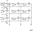
- FIG. 2 is a simplified schematic diagram illustrating an electrical programmable fuse or electrical fuse (eFuse) cell array according to another embodiment of the present invention.
- eFuse array 20 includes n x m eFuse cells, labeled 211,... 21j, ... 21m, 2il,... 2ij, ... 2im, 2nl,... 2nj, ..., 2nm, respectively.
- the following explanation will use eFuse cell 211 as an example.
- Each cell, e. g., eFuse cell 211 includes an eFuse 1110, a first diode 1111, and a second diode 1112.
- Cell 211 also has a read operation MOSFET 2115 between diodes 1112 and a read bit line BL_RD11.
- the gate of MOSFET 2115 is coupled to a read operation control line RD11.
- Other cells in array 20 are similar to cell 211.
- Read operation MOSFET can be an NMOSFET or a PMOSFET, which are coupled between diode 112 and read operation bit line BL_ED11 with either source or drain terminals.
- the read operation MOSFET 2115 in array 20 can be used to select an eFuse cell for the read operation.
- the shared NMOSFET can still reduce the area of the array.
- the shared HVNMOS can make the array smaller than the conventional array having an HVNMOS in each cell. Further, the read current can be increased by the larger shared HVNMOS in embodiments of the invention.
- an eFuse memory device has an array of a plurality of electrical fuse (eFuse) cells that can include n by m eFuse cells arranged in an n by m matrix with n rows and m columns.
- n and m are positive integers equal to or greater than 1.
- the memory device also includes n shared NMOSFETs and m write bit lines.
- I and j are integers equal to or greater than 1.
- the ith shared NMOSFET is coupled to each of the eFuse cells in the ith row.
- the jth write bit line is coupled to the second diode in each of the eFuse cells in the jth column.
- each eFuse cell further includes a read operation MOSFET coupled between the first diode and the read bit line, a gate terminal of the read operation MOSFET being coupled to a read control line.
- the read operation MOSFET is an NMOSFET with a source coupled to the anode of the first diode and a drain coupled to the read bit line.
- the read operation MOSFET is a PMOSFET with a drain coupled to the anode of the first diode and a source coupled to the read bit line.
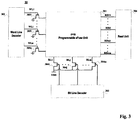
- FIG. 3 is a simplified schematic diagram illustrating a memory device having an electrical programmable fuse or electrical fuse (eFuse) cell array according to an embodiment of the present invention.
- memory device 30 includes an eFuse array 301, which includes an n by m array of eFuse cells, n shared NMOSFETs 3051 to 305n, word line decoder 302, write operation bit line decoder 303, and m bit line PMOSFETs 3041 to 304m.
- the gate of the PMOSFET is coupled to a bit line, and a source is coupled to a power supply VDD.
- Each eFuse cell can be similar to eFuse cell 111 in FIG. 1 or eFuse cell 211 in FIG.
- eFuse cell (i, j) can be written by the decoders selecting word line WLi and bit line BLj to turn on the jth shared NMOSFET and the ith bit line PMOSFET.
- memory device 30 can include an array as shown in FIG. 2 , which includes a read operation MOSFET for each eFuse cell for receiving a read control signal RD11 to RDnm.
- Memory device 30 also includes a read unit 306 providing read control lines RD 11 to RDnm.
- memory device 30 can include an array as shown in FIG. 1 , which does not include a read operation MOSFET for each eFuse cell.
- the read unit 306 can provide a voltage to the read operation bit line to perform the read operation at a cell selected by the word line.
- the memory device of the present invention may also include other components, e.g., PMOS drivers, shared NMOSFET drivers, pass gates, and control circuits, etc. To simplify the description, certain details well-known in the art have been omitted. Those skilled in the art can understand from the description the structure and operations of the memory device.
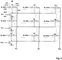
- FIG. 4 is a simplified schematic diagram illustrating an electrical programmable fuse or electrical fuse (eFuse) cell array according to an embodiment of the present invention.
- the electrically programmable fuse cell array 40 includes: n ⁇ m electrically programmable fuse cells, labeled 411, ... 41j,... 41m, 4il,... 4ij,... 4im, 4nl,... 4nj, ..., 4nm, respectively.
- the following explanation will use eFuse cell 411 as an example.
- eFuse cell 411 includes an eFuse 4110 having a first terminal 41101 and a second terminal 41102, and a PNP transistor 4111 having an N-type region 41113, a first P-type region 41111 and a second P-type region 41112.
- P-type region 41111 and N-type region 41113 function similarly to first diode 1111 in FIGS. 1 and 2 .
- P-type region 41112 and N-type region 41113 function similarly to second diode 1112 in FIGS. 1 and 2 .
- P-type region 41111 is coupled to write bit line BL1
- p-type region 41112 is coupled to a read bit line BL_RD11.
- Other components in FIG. 4 are also similar to the corresponding ones in FIG. 1 .
- a shared NMOSFET 4114 has a drain coupled to eFuse 4110, a gate coupled to a word line WL1, and a source coupled to a ground terminal.
- eFuse array 40 The operations of eFuse array 40 are similar to those described above in connection with eFuse array 10 in FIG. 1 . Further, eFuse array 40 can also be used in memory device 30 described in FIG. 3 . Therefore, the descriptions are not repeated here.
- a bipolar is used to replace the two diodes in FIG. 1 . This arrangement can lead to reduced device size. The reduction in device size can come from the smaller bipolar transistor size and reduction of contacts and interconnects.
- FIG. 5 is a simplified schematic diagram illustrating an electrical programmable fuse or electrical fuse (eFuse) cell array according to an embodiment of the present invention.
- the electrically programmable fuse cell array 50 includes: n ⁇ m electrically programmable fuse cells, labeled 511,... 51j,... 51m, 5il,... 5ij,... 5im, 5nl,... 5nj, ..., 5nm, respectively.
- the following explanation will use eFuse cell 511 as an example.
- Each cell, e. g., eFuse cell 511, similar to eFuse cell 411 in FIG. 4 includes an eFuse 4110 and a bipolar transistor 4111.
- eFuse cell 511 also has a read operation MOSFET 5115 disposed between a P type region 41112 and read bit line BL_RD11.
- the gate of MOSFET 5115 is coupled to a read operation control line RD11.
- Read operation MOSFET 5115 can be an NMOSFET or a PMOSFET, similar to cell 211 in FIG. 2 .
- the operations of memory array 50 are similar eFuse cell 211 in FIG. 2 , with a bipolar transistor replacing two diodes.
- an eFuse memory device has an array of a plurality of electrical fuse (eFuse) cells that can include n by m eFuse cells arranged in an n by m matrix with n rows and m columns. n and m are positive integers equal to or greater than 1.
- the memory device also includes n shared NMOSFETs and m write bit lines. In the ith row, the ith shared NMOSFET is coupled to each of the eFuse cells in the ith row. In the jth column, the jth write bit line is coupled to the second diode in each of the eFuse cells in the jth column.
- Each row of eFuse cells shares a word line, and each column of eFuse cells shares a write operation bit line.
- the memory device can include an eFuse array 40 or an eFuse array 50. Therefore, the descriptions are not repeated here.
- eFuse arrays 40 and 50 a bipolar is used to replace the two diodes in FIGS. 1 and 2 . This arrangement can lead to reduced device size. The reduction in device size can come from the smaller bipolar transistor size and reduction of contacts and interconnects.
Landscapes
- Semiconductor Memories (AREA)
- Read Only Memory (AREA)
- Design And Manufacture Of Integrated Circuits (AREA)
Abstract
Description
- This application claims priority to Chinese patent application No.
201510731242.2, filed on November 2, 2015 - The present invention relates to the field of semiconductor technology. Specifically, embodiments of the invention are directed to an electrically programmable fuse (eFuse) cell array and memory device.
- An eFuse is an electrically programmable memory device whose resistance can be changed by passing an electric current through it. It usually can be programmed only one time. Programmed eFuses are electrically high resistance, while unprogrammed eFuses remain in a low resistance state. An eFuse can be implemented using different technologies. For example, an eFuse can be made of a conductive line, which can transition to a high resistance state or can be broken by applying a large current through it. In another example, an eFuse can be made of a polysilicon line coated with a silicide layer. The programming current can cause the silicide layer to redistribute and be broken, resulting in the high resistance state. In computing, an eFuse allows for the dynamic real-time reprogramming of computer chips. By utilizing eFuses, a chip manufacturer can allow for the circuits on a chip to be changed by applying an electrical signal.
- In a conventional eFuse (electrical programmable fuse) array, in order to achieve compatibility, all devices in the eFuse array are core devices. At the 28 nm technology node, for example, the operating voltage in the core devices is very low. The high voltage needed in programming or burning the eFuse can be a challenge. Some conventional methods have been proposed to overcome the high programming voltage eFuse array. For example, an LDO (Low dropout regulator) can be used to reduce the voltage to an acceptable level. However, this approach can result in a large area of the device.
- In some conventional eFuse arrays, each eFise cell has an eFuse and an NMOS transistor connected in series. Here the NMOS can be HVNMOS (high voltage NMOS), in which the gate voltage is close to the programming voltage. However, the area of the HVNMOS area is larger than the core device, resulting in peripheral circuits of such eFuse array becoming relatively large. Therefore, the size of a low capacity eFuse array can be dominated by the LDO circuit, and the size of a high-capacity eFuse can be dominated by the eFuse cell size.
- The high voltage bit line operations in an eFuse array can adversely affect its reliability, e.g., the total number of operations. In addition, it is difficult to reduce the peripheral devices, which can include word line drivers, pass gate drivers, PMOS switches and drivers, as well as level converters, etc.
- The present invention relates to the field of semiconductor technology. Specifically, embodiments of the invention are directed to an electrical (programmable) fuse (eFuse) cell, a compact electrically programmable fuse (eFuse) cell array and a storage unit.
- According to a first aspect of the invention, an electrically (programmable) fuse (eFuse) cell includes first, second, and third terminals, an eFuse, a first diode, and a second diode. The eFuse, the first diode, and the second diode are coupled to an internal node. The first diode is coupled between the first terminal and the internal node, the second diode is coupled between the second terminal and the internal node, and the eFuse is coupled between the third terminal and the internal node.
- Each eFuse cell may include a PNP bipolar transistor, in which the first diode is formed by a first PN junction of the bipolar transistor, the second diode is formed by a second PN junction of the bipolar transistor, and the internal node is a base of the bipolar transistor.
- Accordingly, an electrical (programmable) fuse (eFuse) cell may includes first, second, and third terminals, an eFuse, and a PNP bipolar transistor having a first P-type region, an N-type base region, and a second P-type region. The first terminal is coupled to the first P-type region, the second terminal is coupled to the second P-type region, and the eFuse is coupled between the third terminal and the base region of the bipolar transistor.
- The first terminal may be configured for coupling to a read bit line, the second terminal is configured for coupling to a write bit line; and the third terminal is configured for coupling to a shared NMOSFET, which is configured for coupling to the third terminals of all eFuse cells in a row of an array.
- The eFuse may comprise a conductive material which is configured to transition from a low resistive state to a high resistive state when a programming current is applied. The eFuse may include a polysilicon material with an overlying silicide layer.
- The eFuse may comprise a polysilicon material with an overlying silicide layer.
- According to a second aspect of the present invention, an electrical fuse (eFuse) memory device includes an eFuse array having a plurality of electrical fuse (eFuse) cells according to the first aspect of the invention, which eFuse cells are arranged in multiple rows and columns. Each eFuse cell has an eFuse, a first diode, and a second diode coupled to an internal node, each eFuse cell further having first, second, and third terminals. The first diode is coupled between the first terminal and the internal node, the second diode is coupled between the second terminal and the internal node, and the eFuse is coupled between the third terminal and the internal node. The eFuse array further includes a shared NMOSFET for each of the multiple rows, with a drain coupled to the third terminal of each of the plurality of eFuse cells in that row, the shared NMOSFET having a source coupled to a ground terminal and a gate coupled to a word line. The memory device also has a write bit line and a read bit line for each column. The write bit line is coupled to the second terminal of each of the eFuse cells in that column, and the read bit line is coupled to the first terminal of the eFuse cell.
- As disclosed in connection with the electrical (programmable) fuse (eFuse) cell, each eFuse cell may include a PNP bipolar transistor. In the PNP bipolar transistor the first diode may be formed by a first PN junction of the bipolar transistor, the second diode may be formed by a second PN junction of the bipolar transistor, and the internal node may be a base of the bipolar transistor.
- An anode of the first diode may be coupled to the first terminal. A cathode of the first may be coupled to the internal node.
- An anode of the second diode may be coupled to the second terminal A cathode of the second may be coupled to the internal node.
- The plurality of electrical fuse (eFuse) cells may comprise n by m eFuse cells arranged in an n by m matrix with n rows and m columns, n and m being integers. The memory device may further include n shared NMOSFETs and m write bit lines. In the ith row, "i" being an integer, the ith shared NMOSFET may be coupled to each of the eFuse in the ith row. In the jth column, "j" being an integer, the jth write bit line may be coupled to the second diode in each of the eFuse cells in the jth column.
- Each eFuse cell may also include a read operation MOSFET. The read operation MOSFET may be coupled between the first diode and the read bit line. A gate terminal of the read operation MOSFET may be coupled to a read control line.
- The read operation MOSFET may be an NMOSFET with a source coupled to the anode of the first diode and a drain coupled to the read bit line. Alternatively, the read operation MOSFET may be a PMOSFET with a drain coupled to the anode of the first diode and a source coupled to the read bit line.
- The memory device may also include a word line decoder a write operation decoder, and a read unit.
- The memory device may also include a bit line PMOSFET for each of the m columns.
- Each eFuse cell may be coupled to a read bit line.
- The following description, together with the accompanying drawings, will provide further understanding of the nature and advantages of the claimed invention.
-
-
FIG. 1 is a simplified schematic diagram illustrating an electrical programmable fuse or electrical fuse (eFuse) cell array according to an embodiment of the present invention; -
FIG. 2 is a simplified schematic diagram illustrating an electrical programmable fuse or electrical fuse (eFuse) cell array according to another embodiment of the present invention; -
FIG. 3 is a simplified schematic diagram illustrating a memory device having an electrical programmable fuse or electrical fuse (eFuse) cell array according to an embodiment of the present invention; -
FIG. 4 is a simplified schematic diagram illustrating an electrical programmable fuse or electrical fuse (eFuse) cell array according to embodiment of the present invention; and -
FIG. 5 is a simplified schematic diagram illustrating an electrical programmable fuse or electrical fuse (eFuse) cell array according to an embodiment of the present invention - Exemplary embodiments of the present invention will be described with reference to the figures. The following description of exemplary embodiments is illustrative only, and not intended to be any limitation on the invention and its application or use. It is understood that the relative arrangement of parts and steps and numeric expressions set forth in these embodiments are not to be construed as limiting the scope of the invention, which is only defined by the claims. It is also understood that, for convenience of description, the size of the various components shown in the drawings are not necessarily drawn in actual proportional relationship. Techniques, methods and devices known to one of ordinary skill in the relevant art may not be discussed in detail, but in situations in which these techniques, methods and apparatus apply, these techniques, methods and apparatus should be considered as part of this specification. Further, similar reference numerals and letters are used to refer to similar items in the following figures, and once an item is defined in one of the figures, it will not need to be explained further in the subsequent figures.
-
FIG. 1 is a simplified schematic diagram illustrating an electrical programmable fuse or electrical fuse (eFuse) cell array according to an embodiment of the present invention. As shown inFIG. 1 , the electrically programmablefuse cell array 10 includes n × m electrically programmable fuse cells, labeled 111,... 11j, ... 11m, 1il, ... 1ij, ... 1im, 1nl, ... 1nj, ..., 1nm, respectively. The following explanation will useeFuse cell 111 as an example. - As shown in
FIG. 1 ,eFuse cell 111 includes aneFuse 1110, afirst diode 1111, and asecond diode 1112. Electrical programmable fuse or electrical fuse (eFuse) 1110 includes afirst terminal 11101 and asecond terminal 11102. Depending on the embodiments,diode 1111 can have a cathode coupled toeFuse 1110 and an anode coupled to a write bit line BL1.Diode 1112 can have a cathode coupled toeFuse 1110 and an anode coupled to a read bit line BL_RD11. The eFuse cells in the same row aseFuse cell 111 are connected to a sharedNMOSFET 1114, which has a drain coupled toeFuse 1110, a gate coupled to a word line WL1, and a source coupled to a ground terminal. Other eFuse cells ineFuse cell array 10 are similar toeFuse cell 111, as shown inFIG. 1 . - In conventional eFuse memories, each eFuse cell usually has an NMOS transistor, which occupied most of the area of the device. In embodiments of the invention, each row of the eFuse cells shares a shared NMOSFET (for example HVNMOS). Although each of the eFuse cells has two additional diodes, the overall area of the eFuse array can be reduced, thereby reducing the size of the device.
- In some embodiments, the central core the device may operate at a voltage 1.05 V, and a voltage over 1.26V may cause reliability problems. Since the read operation is carried out with a voltage of 1.05 V, the diodes and other associated circuitry can be low-voltage core devices. Using low-voltage components can also reduce the device area.
- In a write operation to
cell 111, a high voltage is applied to write bit line BL1, another high voltage is applied to word line WL, andNMOSFET 1114 is turned on. A write current flows through write bit line BL1,diode 1111,fuse 1110, and sharedNMOSFET 1114. This current causes fuse 1110 to be blown or transition to a high resistance state. Here, a fuse being "blown" can mean the fuse is literally broken, or it can mean the fuse resistance is increased by several orders of magnitude. In this embodiment, fusecell 111 is referred to having been written with a value of "1." The diode limits the direction of the write current, and electron migration (EM) effect can cause the fuse to be blown. - The
first diode 1111 in each eFuse cell can serve as a protection device when the cell is not being written. For example, whencell 111 is being written andcell 11j is not being written, A voltage of 5 V is applied to write bit line BL1, and a voltage of 1V is applied to write bit line BLj. In this case, the diode incell 11j can block a current flowing from the shared NMOSFET througheFuse 11j.Cell 11j is therefore protected. - In a read operation to
cell 111, a voltage is applied to read bit line BL_RD11, another voltage is applied to word line WL1, and shared NMOSFET 114 is turned on. A current flowing through this path can be used to determine the resistance ofeFuse 1110. Depending on the resistance, it can be determined if the fuse is blown, and a value "1" or "0" can be determined. The read current is selected to be much lower than the write current to prevent damaging the fuse. For example, if a write current has a magnitude of 100 units, and the fuse has a safety rating of 10 units, the read current can be set at 1 unit to ensure reliability of the fuses. - In a conventional memory array, a long bit line is connected to many eFuse cells. The long bit line and the NMOS in each cell can present substantial capacitance. In embodiments of the invention, a diode in each cell is connected to the bit line. With the lower capacitance, the read speed can be increased.
- The first and second diodes in each cell can prevent disturbance to adjacent cells during cell operation. For example, in a write operation, the first diode is forward biased, and the second diode is reverse biased which can prevent disturbing an adjacent cell. Similarly, in a read operation, the first diode is reverse biased, and the second diode is forward biased which can prevent disturbing an adjacent cell.
-
FIG. 2 is a simplified schematic diagram illustrating an electrical programmable fuse or electrical fuse (eFuse) cell array according to another embodiment of the present invention. As shown inFIG 2 ,eFuse array 20 includes n x m eFuse cells, labeled 211,... 21j, ... 21m, 2il,... 2ij, ... 2im, 2nl,... 2nj, ..., 2nm, respectively. The following explanation will useeFuse cell 211 as an example. Each cell, e. g.,eFuse cell 211, includes aneFuse 1110, afirst diode 1111, and asecond diode 1112.Cell 211 also has a readoperation MOSFET 2115 betweendiodes 1112 and a read bit line BL_RD11. The gate ofMOSFET 2115 is coupled to a read operation control line RD11. Other cells inarray 20 are similar tocell 211. Read operation MOSFET can be an NMOSFET or a PMOSFET, which are coupled between diode 112 and read operation bit line BL_ED11 with either source or drain terminals. Compared witharray 10 inFIG. 1 , theread operation MOSFET 2115 inarray 20 can be used to select an eFuse cell for the read operation. The shared NMOSFET can still reduce the area of the array. - In embodiments of the invention, the shared HVNMOS can make the array smaller than the conventional array having an HVNMOS in each cell. Further, the read current can be increased by the larger shared HVNMOS in embodiments of the invention.
- In some embodiments, an eFuse memory device has an array of a plurality of electrical fuse (eFuse) cells that can include n by m eFuse cells arranged in an n by m matrix with n rows and m columns. Here, n and m are positive integers equal to or greater than 1. The memory device also includes n shared NMOSFETs and m write bit lines. In the following description, I and j are integers equal to or greater than 1. In the ith row, the ith shared NMOSFET is coupled to each of the eFuse cells in the ith row. In the jth column, the jth write bit line is coupled to the second diode in each of the eFuse cells in the jth column. Each row of eFuse cells share a word line, and each column of eFuse cells shares a write operation bit line. In some embodiments, each eFuse cell further includes a read operation MOSFET coupled between the first diode and the read bit line, a gate terminal of the read operation MOSFET being coupled to a read control line. In some embodiments, the read operation MOSFET is an NMOSFET with a source coupled to the anode of the first diode and a drain coupled to the read bit line. In some embodiments, the read operation MOSFET is a PMOSFET with a drain coupled to the anode of the first diode and a source coupled to the read bit line.
-
FIG. 3 is a simplified schematic diagram illustrating a memory device having an electrical programmable fuse or electrical fuse (eFuse) cell array according to an embodiment of the present invention. As shown inFIG. 3 ,memory device 30 includes aneFuse array 301, which includes an n by m array of eFuse cells, n sharedNMOSFETs 3051 to 305n,word line decoder 302, write operationbit line decoder 303, and mbit line PMOSFETs 3041 to 304m. The gate of the PMOSFET is coupled to a bit line, and a source is coupled to a power supply VDD. Each eFuse cell can be similar toeFuse cell 111 inFIG. 1 oreFuse cell 211 inFIG. 2 as described above. The word line and bit line arrangement is also similar to those described in connection toFIGS. 1 and2 . In a write operation, eFuse cell (i, j) can be written by the decoders selecting word line WLi and bit line BLj to turn on the jth shared NMOSFET and the ith bit line PMOSFET. - In some embodiments,
memory device 30 can include an array as shown inFIG. 2 , which includes a read operation MOSFET for each eFuse cell for receiving a read control signal RD11 to RDnm.Memory device 30 also includes aread unit 306 providing read control lines RD 11 to RDnm. - In some embodiments,
memory device 30 can include an array as shown inFIG. 1 , which does not include a read operation MOSFET for each eFuse cell. In this case, theread unit 306 can provide a voltage to the read operation bit line to perform the read operation at a cell selected by the word line. - Those skilled in the art will understand that the memory device of the present invention may also include other components, e.g., PMOS drivers, shared NMOSFET drivers, pass gates, and control circuits, etc. To simplify the description, certain details well-known in the art have been omitted. Those skilled in the art can understand from the description the structure and operations of the memory device.
-
FIG. 4 is a simplified schematic diagram illustrating an electrical programmable fuse or electrical fuse (eFuse) cell array according to an embodiment of the present invention. As shown inFIG. 4 , the electrically programmablefuse cell array 40 includes: n × m electrically programmable fuse cells, labeled 411, ... 41j,... 41m, 4il,... 4ij,... 4im, 4nl,... 4nj, ..., 4nm, respectively. The following explanation will useeFuse cell 411 as an example. - As shown in
FIG. 4 ,eFuse cell 411 includes aneFuse 4110 having afirst terminal 41101 and asecond terminal 41102, and aPNP transistor 4111 having an N-type region 41113, a first P-type region 41111 and a second P-type region 41112. In this embodiments, P-type region 41111 and N-type region 41113 function similarly tofirst diode 1111 inFIGS. 1 and2 . P-type region 41112 and N-type region 41113 function similarly tosecond diode 1112 inFIGS. 1 and2 . P-type region 41111 is coupled to write bit line BL1, and p-type region 41112 is coupled to a read bit line BL_RD11. Other components inFIG. 4 are also similar to the corresponding ones inFIG. 1 . For example, a sharedNMOSFET 4114 has a drain coupled toeFuse 4110, a gate coupled to a word line WL1, and a source coupled to a ground terminal. - The operations of
eFuse array 40 are similar to those described above in connection witheFuse array 10 inFIG. 1 . Further,eFuse array 40 can also be used inmemory device 30 described inFIG. 3 . Therefore, the descriptions are not repeated here. IneFuse array 40, a bipolar is used to replace the two diodes inFIG. 1 . This arrangement can lead to reduced device size. The reduction in device size can come from the smaller bipolar transistor size and reduction of contacts and interconnects. -
FIG. 5 is a simplified schematic diagram illustrating an electrical programmable fuse or electrical fuse (eFuse) cell array according to an embodiment of the present invention. As shown inFIG. 5 , the electrically programmablefuse cell array 50 includes: n × m electrically programmable fuse cells, labeled 511,... 51j,... 51m, 5il,... 5ij,... 5im, 5nl,... 5nj, ..., 5nm, respectively. The following explanation will useeFuse cell 511 as an example. Each cell, e. g.,eFuse cell 511, similar toeFuse cell 411 inFIG. 4 , includes aneFuse 4110 and abipolar transistor 4111. UnlikeeFuse cell 411,eFuse cell 511 also has a readoperation MOSFET 5115 disposed between aP type region 41112 and read bit line BL_RD11. The gate ofMOSFET 5115 is coupled to a read operation control line RD11. Readoperation MOSFET 5115 can be an NMOSFET or a PMOSFET, similar tocell 211 inFIG. 2 . The operations ofmemory array 50 aresimilar eFuse cell 211 inFIG. 2 , with a bipolar transistor replacing two diodes. - In some embodiments, an eFuse memory device has an array of a plurality of electrical fuse (eFuse) cells that can include n by m eFuse cells arranged in an n by m matrix with n rows and m columns. n and m are positive integers equal to or greater than 1. The memory device also includes n shared NMOSFETs and m write bit lines. In the ith row, the ith shared NMOSFET is coupled to each of the eFuse cells in the ith row. In the jth column, the jth write bit line is coupled to the second diode in each of the eFuse cells in the jth column. Each row of eFuse cells shares a word line, and each column of eFuse cells shares a write operation bit line. The memory device can include an
eFuse array 40 or aneFuse array 50. Therefore, the descriptions are not repeated here. IneFuse arrays FIGS. 1 and2 . This arrangement can lead to reduced device size. The reduction in device size can come from the smaller bipolar transistor size and reduction of contacts and interconnects.
Claims (14)
- An electrically programmable fuse, eFuse, cell, comprising:first, second, and third terminals;an eFuse;a first diode; anda second diode;wherein:the eFuse, the first diode, and the second diode are coupled to an internal node,the first diode is coupled between the first terminal and the internal node;the second diode is coupled between the second terminal and the internal node; andthe eFuse is coupled between the third terminal and the internal node.
- The eFuse cell of claim 1, wherein:the first terminal is configured for coupling to a read bit line;the second terminal is configured for coupling to a write bit line; andthe third terminal is configured for coupling to a shared NMOSFET, the shared NMOSFET configured for coupling to the third terminals of all eFuse cells in a row of an array.
- The eFuse cell of claim 1 or 2, wherein each eFuse cell comprises a PNP bipolar transistor, wherein the first diode is formed by a first PN junction of the bipolar transistor, the second diode is formed by a second PN junction of the bipolar transistor, and the internal node is a base of the bipolar transistor.
- The eFuse cell of any one of the claims1-3, wherein the eFuse comprises a conductive material which is configured to transition from a low resistive state to a high resistive state when a programming current is applied.
- The eFuse cell of any one of the claims 1-4, wherein the eFuse comprises a polysilicon material with an overlying silicide layer.
- An eFuse memory device, comprising:an eFuse array having a plurality of eFuse cells according to claim 2 which are arranged in multiple rows and columns, wherein: the shared NMOSFET is for each of the multiple rows, with a drain coupled to the third terminal of each of the plurality of eFuse cells in that row, a source coupled to a ground terminal, and a gate coupled to a word line;the write bit line is for each column, wherein the write bit line is coupled to the second terminal of each of the eFuse cells in that column; andthe read bit line is for each column, wherein the read bit line coupled to the first terminal of the eFuse cell.
- The memory device of claim 6, wherein each eFuse cell comprises a PNP bipolar transistor, wherein the first diode is formed by a first PN junction of the bipolar transistor, the second diode is formed by a second PN junction of the bipolar transistor, and the internal node is a base of the bipolar transistor.
- The memory device of claim 6 or 7, wherein an anode of the first diode is coupled to the first terminal, and a cathode of the first diode is coupled to the internal node, and
wherein an anode of the second diode is coupled to the second terminal, and a cathode of the second is coupled to the internal node. - The memory device of any one of the claims 6-8, wherein the plurality of eFuse cells comprises n by m eFuse cells arranged in an n by m matrix with n rows and m columns, n and m being integers;
the memory device further comprises n shared NMOSFETs and m write bit lines;
in the ith row, "i" being an integer, the ith shared NMOSFET is coupled to each of the eFuse cells in the ith row;
in the jth column, "j" being an integer, the jth write bit line is coupled to the second diode in each of the eFuse cells in the jth column. - The memory device of any one of the claims 6-9, wherein each eFuse cell further comprises a read operation MOSFET coupled between the first diode and the read bit line, a gate terminal of the read operation MOSFET being coupled to a read control line,
wherein preferably the read operation MOSFET is an NMOSFET with a source coupled to the anode of the first diode and a drain coupled to the read bit line, or the read operation MOSFET is a PMOSFET with a drain coupled to the anode of the first diode and a source coupled to the read bit line. - The memory device of any one of the claims 6-10, further comprising a word line decoder and write operation decoder, and a read unit.
- The memory device of any one of the claims 6-11, further comprising a bit line PMOSFET for each of the m columns.
- The memory device of any one of the claims 6-12, wherein each eFuse cell is coupled to a read bit line.
- The memory device of any one of the claims 6-13, wherein each eFuse cell comprises a conductive material which is configured to transition from a low resistive state to a high resistive state when a programming current is applied.
Applications Claiming Priority (1)
| Application Number | Priority Date | Filing Date | Title |
|---|---|---|---|
| CN201510731242.2A CN106653081B (en) | 2015-11-02 | 2015-11-02 | Electrically programmable fuse cell, array and memory cell |
Publications (2)
| Publication Number | Publication Date |
|---|---|
| EP3163580A1 true EP3163580A1 (en) | 2017-05-03 |
| EP3163580B1 EP3163580B1 (en) | 2019-09-04 |
Family
ID=57209299
Family Applications (1)
| Application Number | Title | Priority Date | Filing Date |
|---|---|---|---|
| EP16196134.7A Active EP3163580B1 (en) | 2015-11-02 | 2016-10-27 | Method and device for compact efuse array |
Country Status (3)
| Country | Link |
|---|---|
| US (1) | US9754680B2 (en) |
| EP (1) | EP3163580B1 (en) |
| CN (1) | CN106653081B (en) |
Families Citing this family (7)
| Publication number | Priority date | Publication date | Assignee | Title |
|---|---|---|---|---|
| KR102284263B1 (en) | 2019-10-29 | 2021-07-30 | 주식회사 키 파운드리 | Electrical-Fuse Cell and Non Volatile memory device having the same |
| US11145379B2 (en) * | 2019-10-29 | 2021-10-12 | Key Foundry Co., Ltd. | Electronic fuse cell array structure |
| DE102021101874B4 (en) * | 2020-06-03 | 2024-07-18 | Taiwan Semiconductor Manufacturing Co., Ltd. | MEMORY CIRCUIT AND METHOD OF OPERATING THE SAME |
| US11791005B2 (en) | 2020-06-03 | 2023-10-17 | Taiwan Semiconductor Manufacturing Company, Ltd. | Memory circuit and method of operating same |
| US11250924B1 (en) * | 2020-10-20 | 2022-02-15 | Qualcomm Incorporated | One-time programmable (OTP) memory cell circuits employing a diode circuit for area reduction, and related OTP memory cell array circuits and methods |
| CN113078160A (en) * | 2021-03-30 | 2021-07-06 | 上海华力微电子有限公司 | Electrically programmable fuse unit and electrically programmable fuse array |
| CN114360617A (en) * | 2021-11-30 | 2022-04-15 | 上海华力集成电路制造有限公司 | Euse unit, application circuit of efuse unit and efuse array |
Citations (2)
| Publication number | Priority date | Publication date | Assignee | Title |
|---|---|---|---|---|
| US20120020177A1 (en) * | 2010-07-20 | 2012-01-26 | Taiwan Semiconductor Manufacturing Company, Ltd. | Electrical fuse memory |
| US20150243365A1 (en) * | 2014-02-25 | 2015-08-27 | Freescale Semiconductor, Inc. | Antifuse with bypass diode and method thereof |
Family Cites Families (12)
| Publication number | Priority date | Publication date | Assignee | Title |
|---|---|---|---|---|
| JP2001244338A (en) * | 2000-02-25 | 2001-09-07 | Toshiba Corp | Semiconductor integrated circuit device, semiconductor integrated circuit mounting substrate device, and input protection function release method for semiconductor integrated circuit device |
| US6385075B1 (en) * | 2001-06-05 | 2002-05-07 | Hewlett-Packard Company | Parallel access of cross-point diode memory arrays |
| US7212454B2 (en) * | 2005-06-22 | 2007-05-01 | Sandisk 3D Llc | Method and apparatus for programming a memory array |
| US8014185B2 (en) * | 2008-07-09 | 2011-09-06 | Sandisk 3D Llc | Multiple series passive element matrix cell for three-dimensional arrays |
| CN101908548B (en) * | 2009-06-04 | 2012-06-13 | 北京兆易创新科技有限公司 | Disposal programmable memorizer, manufacturing method thereof and programming reading method thereof |
| US8331126B2 (en) * | 2010-06-28 | 2012-12-11 | Qualcomm Incorporated | Non-volatile memory with split write and read bitlines |
| US9025357B2 (en) * | 2010-08-20 | 2015-05-05 | Shine C. Chung | Programmable resistive memory unit with data and reference cells |
| US8576602B2 (en) * | 2010-08-20 | 2013-11-05 | Shine C. Chung | One-time programmable memories using polysilicon diodes as program selectors |
| US9818478B2 (en) * | 2012-12-07 | 2017-11-14 | Attopsemi Technology Co., Ltd | Programmable resistive device and memory using diode as selector |
| US9019742B2 (en) * | 2010-08-20 | 2015-04-28 | Shine C. Chung | Multiple-state one-time programmable (OTP) memory to function as multi-time programmable (MTP) memory |
| US9431127B2 (en) * | 2010-08-20 | 2016-08-30 | Shine C. Chung | Circuit and system of using junction diode as program selector for metal fuses for one-time programmable devices |
| US9324447B2 (en) * | 2012-11-20 | 2016-04-26 | Shine C. Chung | Circuit and system for concurrently programming multiple bits of OTP memory devices |
-
2015
- 2015-11-02 CN CN201510731242.2A patent/CN106653081B/en active Active
-
2016
- 2016-10-27 US US15/336,365 patent/US9754680B2/en active Active
- 2016-10-27 EP EP16196134.7A patent/EP3163580B1/en active Active
Patent Citations (2)
| Publication number | Priority date | Publication date | Assignee | Title |
|---|---|---|---|---|
| US20120020177A1 (en) * | 2010-07-20 | 2012-01-26 | Taiwan Semiconductor Manufacturing Company, Ltd. | Electrical fuse memory |
| US20150243365A1 (en) * | 2014-02-25 | 2015-08-27 | Freescale Semiconductor, Inc. | Antifuse with bypass diode and method thereof |
Also Published As
| Publication number | Publication date |
|---|---|
| EP3163580B1 (en) | 2019-09-04 |
| CN106653081B (en) | 2020-04-10 |
| US20170125120A1 (en) | 2017-05-04 |
| US9754680B2 (en) | 2017-09-05 |
| CN106653081A (en) | 2017-05-10 |
Similar Documents
| Publication | Publication Date | Title |
|---|---|---|
| EP3163580B1 (en) | Method and device for compact efuse array | |
| US8760955B2 (en) | Electrical fuse memory arrays | |
| US20100232203A1 (en) | Electrical anti-fuse and related applications | |
| US7688613B2 (en) | Method and system for controlling multiple electrical fuses with one program device | |
| US11145379B2 (en) | Electronic fuse cell array structure | |
| US20100165699A1 (en) | Antifuse programmable memory array | |
| TWI445137B (en) | Single-time programmable memory, electronic system, electrical fuse memory, programmable resistive memory and method thereof | |
| EP2867922A2 (en) | Integrated circuit device featuring an antifuse and method of making same | |
| EP1920441A2 (en) | Random access electrically programmable-e-fuse rom | |
| US11538541B2 (en) | Semiconductor device having a diode type electrical fuse (e-fuse) cell array | |
| US10672489B2 (en) | Electronic device with a fuse array mechanism | |
| US7269081B2 (en) | Program circuit of semiconductor | |
| US11785766B2 (en) | E-fuse | |
| US20240046992A1 (en) | Electrical fuse one time programmable (otp) memory | |
| US20130279282A1 (en) | E-fuse array circuit | |
| US7110278B2 (en) | Crosspoint memory array utilizing one time programmable antifuse cells | |
| US12014796B2 (en) | Memory device and method of operating the same | |
| US9786382B1 (en) | Semiconductor device and memory element | |
| US11211135B2 (en) | Fuse storage cell, storage array, and operation method of storage array | |
| JPWO2020158531A1 (en) | Storage device and programming method | |
| KR102342532B1 (en) | Non-Volatile Memory Device having a Fuse Type Cell Array | |
| KR101762920B1 (en) | One-time programmable memory apparatus | |
| US20090219747A1 (en) | Method of programming a memory having electrically programmable fuses | |
| US12347504B2 (en) | One-time-programmable memory devices | |
| US12531117B2 (en) | Semiconductor device and programmable macro circuit |
Legal Events
| Date | Code | Title | Description |
|---|---|---|---|
| PUAI | Public reference made under article 153(3) epc to a published international application that has entered the european phase |
Free format text: ORIGINAL CODE: 0009012 |
|
| STAA | Information on the status of an ep patent application or granted ep patent |
Free format text: STATUS: THE APPLICATION HAS BEEN PUBLISHED |
|
| AK | Designated contracting states |
Kind code of ref document: A1 Designated state(s): AL AT BE BG CH CY CZ DE DK EE ES FI FR GB GR HR HU IE IS IT LI LT LU LV MC MK MT NL NO PL PT RO RS SE SI SK SM TR |
|
| AX | Request for extension of the european patent |
Extension state: BA ME |
|
| RAP1 | Party data changed (applicant data changed or rights of an application transferred) |
Owner name: SEMICONDUCTOR MANUFACTURING INTERNATIONAL CORPORAT |
|
| STAA | Information on the status of an ep patent application or granted ep patent |
Free format text: STATUS: REQUEST FOR EXAMINATION WAS MADE |
|
| 17P | Request for examination filed |
Effective date: 20171020 |
|
| RBV | Designated contracting states (corrected) |
Designated state(s): AL AT BE BG CH CY CZ DE DK EE ES FI FR GB GR HR HU IE IS IT LI LT LU LV MC MK MT NL NO PL PT RO RS SE SI SK SM TR |
|
| STAA | Information on the status of an ep patent application or granted ep patent |
Free format text: STATUS: EXAMINATION IS IN PROGRESS |
|
| 17Q | First examination report despatched |
Effective date: 20180315 |
|
| RAP1 | Party data changed (applicant data changed or rights of an application transferred) |
Owner name: SEMICONDUCTOR MANUFACTURING INTERNATIONAL (BEIJING Owner name: SEMICONDUCTOR MANUFACTURING INTERNATIONAL (SHANGHA |
|
| GRAJ | Information related to disapproval of communication of intention to grant by the applicant or resumption of examination proceedings by the epo deleted |
Free format text: ORIGINAL CODE: EPIDOSDIGR1 |
|
| STAA | Information on the status of an ep patent application or granted ep patent |
Free format text: STATUS: GRANT OF PATENT IS INTENDED |
|
| GRAP | Despatch of communication of intention to grant a patent |
Free format text: ORIGINAL CODE: EPIDOSNIGR1 |
|
| RIC1 | Information provided on ipc code assigned before grant |
Ipc: G11C 17/18 20060101ALI20190403BHEP Ipc: G11C 17/16 20060101AFI20190403BHEP |
|
| INTG | Intention to grant announced |
Effective date: 20190429 |
|
| RIN1 | Information on inventor provided before grant (corrected) |
Inventor name: YANG, CHIACHI |
|
| GRAS | Grant fee paid |
Free format text: ORIGINAL CODE: EPIDOSNIGR3 |
|
| GRAA | (expected) grant |
Free format text: ORIGINAL CODE: 0009210 |
|
| STAA | Information on the status of an ep patent application or granted ep patent |
Free format text: STATUS: THE PATENT HAS BEEN GRANTED |
|
| AK | Designated contracting states |
Kind code of ref document: B1 Designated state(s): AL AT BE BG CH CY CZ DE DK EE ES FI FR GB GR HR HU IE IS IT LI LT LU LV MC MK MT NL NO PL PT RO RS SE SI SK SM TR |
|
| REG | Reference to a national code |
Ref country code: GB Ref legal event code: FG4D |
|
| REG | Reference to a national code |
Ref country code: CH Ref legal event code: EP |
|
| REG | Reference to a national code |
Ref country code: AT Ref legal event code: REF Ref document number: 1176507 Country of ref document: AT Kind code of ref document: T Effective date: 20190915 |
|
| REG | Reference to a national code |
Ref country code: DE Ref legal event code: R096 Ref document number: 602016019801 Country of ref document: DE |
|
| REG | Reference to a national code |
Ref country code: IE Ref legal event code: FG4D |
|
| REG | Reference to a national code |
Ref country code: NL Ref legal event code: FP |
|
| REG | Reference to a national code |
Ref country code: LT Ref legal event code: MG4D |
|
| PG25 | Lapsed in a contracting state [announced via postgrant information from national office to epo] |
Ref country code: NO Free format text: LAPSE BECAUSE OF FAILURE TO SUBMIT A TRANSLATION OF THE DESCRIPTION OR TO PAY THE FEE WITHIN THE PRESCRIBED TIME-LIMIT Effective date: 20191204 Ref country code: HR Free format text: LAPSE BECAUSE OF FAILURE TO SUBMIT A TRANSLATION OF THE DESCRIPTION OR TO PAY THE FEE WITHIN THE PRESCRIBED TIME-LIMIT Effective date: 20190904 Ref country code: SE Free format text: LAPSE BECAUSE OF FAILURE TO SUBMIT A TRANSLATION OF THE DESCRIPTION OR TO PAY THE FEE WITHIN THE PRESCRIBED TIME-LIMIT Effective date: 20190904 Ref country code: FI Free format text: LAPSE BECAUSE OF FAILURE TO SUBMIT A TRANSLATION OF THE DESCRIPTION OR TO PAY THE FEE WITHIN THE PRESCRIBED TIME-LIMIT Effective date: 20190904 Ref country code: LT Free format text: LAPSE BECAUSE OF FAILURE TO SUBMIT A TRANSLATION OF THE DESCRIPTION OR TO PAY THE FEE WITHIN THE PRESCRIBED TIME-LIMIT Effective date: 20190904 Ref country code: BG Free format text: LAPSE BECAUSE OF FAILURE TO SUBMIT A TRANSLATION OF THE DESCRIPTION OR TO PAY THE FEE WITHIN THE PRESCRIBED TIME-LIMIT Effective date: 20191204 |
|
| PGFP | Annual fee paid to national office [announced via postgrant information from national office to epo] |
Ref country code: NL Payment date: 20191021 Year of fee payment: 4 |
|
| PG25 | Lapsed in a contracting state [announced via postgrant information from national office to epo] |
Ref country code: AL Free format text: LAPSE BECAUSE OF FAILURE TO SUBMIT A TRANSLATION OF THE DESCRIPTION OR TO PAY THE FEE WITHIN THE PRESCRIBED TIME-LIMIT Effective date: 20190904 Ref country code: ES Free format text: LAPSE BECAUSE OF FAILURE TO SUBMIT A TRANSLATION OF THE DESCRIPTION OR TO PAY THE FEE WITHIN THE PRESCRIBED TIME-LIMIT Effective date: 20190904 Ref country code: LV Free format text: LAPSE BECAUSE OF FAILURE TO SUBMIT A TRANSLATION OF THE DESCRIPTION OR TO PAY THE FEE WITHIN THE PRESCRIBED TIME-LIMIT Effective date: 20190904 Ref country code: RS Free format text: LAPSE BECAUSE OF FAILURE TO SUBMIT A TRANSLATION OF THE DESCRIPTION OR TO PAY THE FEE WITHIN THE PRESCRIBED TIME-LIMIT Effective date: 20190904 Ref country code: GR Free format text: LAPSE BECAUSE OF FAILURE TO SUBMIT A TRANSLATION OF THE DESCRIPTION OR TO PAY THE FEE WITHIN THE PRESCRIBED TIME-LIMIT Effective date: 20191205 |
|
| PGFP | Annual fee paid to national office [announced via postgrant information from national office to epo] |
Ref country code: FR Payment date: 20191028 Year of fee payment: 4 Ref country code: IT Payment date: 20191031 Year of fee payment: 4 |
|
| REG | Reference to a national code |
Ref country code: AT Ref legal event code: MK05 Ref document number: 1176507 Country of ref document: AT Kind code of ref document: T Effective date: 20190904 |
|
| PG25 | Lapsed in a contracting state [announced via postgrant information from national office to epo] |
Ref country code: PT Free format text: LAPSE BECAUSE OF FAILURE TO SUBMIT A TRANSLATION OF THE DESCRIPTION OR TO PAY THE FEE WITHIN THE PRESCRIBED TIME-LIMIT Effective date: 20200106 Ref country code: RO Free format text: LAPSE BECAUSE OF FAILURE TO SUBMIT A TRANSLATION OF THE DESCRIPTION OR TO PAY THE FEE WITHIN THE PRESCRIBED TIME-LIMIT Effective date: 20190904 Ref country code: EE Free format text: LAPSE BECAUSE OF FAILURE TO SUBMIT A TRANSLATION OF THE DESCRIPTION OR TO PAY THE FEE WITHIN THE PRESCRIBED TIME-LIMIT Effective date: 20190904 Ref country code: PL Free format text: LAPSE BECAUSE OF FAILURE TO SUBMIT A TRANSLATION OF THE DESCRIPTION OR TO PAY THE FEE WITHIN THE PRESCRIBED TIME-LIMIT Effective date: 20190904 Ref country code: AT Free format text: LAPSE BECAUSE OF FAILURE TO SUBMIT A TRANSLATION OF THE DESCRIPTION OR TO PAY THE FEE WITHIN THE PRESCRIBED TIME-LIMIT Effective date: 20190904 |
|
| PG25 | Lapsed in a contracting state [announced via postgrant information from national office to epo] |
Ref country code: IS Free format text: LAPSE BECAUSE OF FAILURE TO SUBMIT A TRANSLATION OF THE DESCRIPTION OR TO PAY THE FEE WITHIN THE PRESCRIBED TIME-LIMIT Effective date: 20200224 Ref country code: SM Free format text: LAPSE BECAUSE OF FAILURE TO SUBMIT A TRANSLATION OF THE DESCRIPTION OR TO PAY THE FEE WITHIN THE PRESCRIBED TIME-LIMIT Effective date: 20190904 Ref country code: SK Free format text: LAPSE BECAUSE OF FAILURE TO SUBMIT A TRANSLATION OF THE DESCRIPTION OR TO PAY THE FEE WITHIN THE PRESCRIBED TIME-LIMIT Effective date: 20190904 Ref country code: CZ Free format text: LAPSE BECAUSE OF FAILURE TO SUBMIT A TRANSLATION OF THE DESCRIPTION OR TO PAY THE FEE WITHIN THE PRESCRIBED TIME-LIMIT Effective date: 20190904 |
|
| REG | Reference to a national code |
Ref country code: CH Ref legal event code: PL |
|
| REG | Reference to a national code |
Ref country code: DE Ref legal event code: R097 Ref document number: 602016019801 Country of ref document: DE |
|
| PLBE | No opposition filed within time limit |
Free format text: ORIGINAL CODE: 0009261 |
|
| STAA | Information on the status of an ep patent application or granted ep patent |
Free format text: STATUS: NO OPPOSITION FILED WITHIN TIME LIMIT |
|
| PG2D | Information on lapse in contracting state deleted |
Ref country code: IS |
|
| PG25 | Lapsed in a contracting state [announced via postgrant information from national office to epo] |
Ref country code: DK Free format text: LAPSE BECAUSE OF FAILURE TO SUBMIT A TRANSLATION OF THE DESCRIPTION OR TO PAY THE FEE WITHIN THE PRESCRIBED TIME-LIMIT Effective date: 20190904 Ref country code: LU Free format text: LAPSE BECAUSE OF NON-PAYMENT OF DUE FEES Effective date: 20191027 Ref country code: CH Free format text: LAPSE BECAUSE OF NON-PAYMENT OF DUE FEES Effective date: 20191031 Ref country code: LI Free format text: LAPSE BECAUSE OF NON-PAYMENT OF DUE FEES Effective date: 20191031 Ref country code: IS Free format text: LAPSE BECAUSE OF FAILURE TO SUBMIT A TRANSLATION OF THE DESCRIPTION OR TO PAY THE FEE WITHIN THE PRESCRIBED TIME-LIMIT Effective date: 20200105 |
|
| 26N | No opposition filed |
Effective date: 20200605 |
|
| REG | Reference to a national code |
Ref country code: BE Ref legal event code: MM Effective date: 20191031 |
|
| PG25 | Lapsed in a contracting state [announced via postgrant information from national office to epo] |
Ref country code: MC Free format text: LAPSE BECAUSE OF FAILURE TO SUBMIT A TRANSLATION OF THE DESCRIPTION OR TO PAY THE FEE WITHIN THE PRESCRIBED TIME-LIMIT Effective date: 20190904 Ref country code: BE Free format text: LAPSE BECAUSE OF NON-PAYMENT OF DUE FEES Effective date: 20191031 Ref country code: SI Free format text: LAPSE BECAUSE OF FAILURE TO SUBMIT A TRANSLATION OF THE DESCRIPTION OR TO PAY THE FEE WITHIN THE PRESCRIBED TIME-LIMIT Effective date: 20190904 |
|
| PG25 | Lapsed in a contracting state [announced via postgrant information from national office to epo] |
Ref country code: IE Free format text: LAPSE BECAUSE OF NON-PAYMENT OF DUE FEES Effective date: 20191027 |
|
| PG25 | Lapsed in a contracting state [announced via postgrant information from national office to epo] |
Ref country code: CY Free format text: LAPSE BECAUSE OF FAILURE TO SUBMIT A TRANSLATION OF THE DESCRIPTION OR TO PAY THE FEE WITHIN THE PRESCRIBED TIME-LIMIT Effective date: 20190904 |
|
| REG | Reference to a national code |
Ref country code: NL Ref legal event code: MM Effective date: 20201101 |
|
| GBPC | Gb: european patent ceased through non-payment of renewal fee |
Effective date: 20201027 |
|
| PG25 | Lapsed in a contracting state [announced via postgrant information from national office to epo] |
Ref country code: FR Free format text: LAPSE BECAUSE OF NON-PAYMENT OF DUE FEES Effective date: 20201031 Ref country code: NL Free format text: LAPSE BECAUSE OF NON-PAYMENT OF DUE FEES Effective date: 20201101 Ref country code: MT Free format text: LAPSE BECAUSE OF FAILURE TO SUBMIT A TRANSLATION OF THE DESCRIPTION OR TO PAY THE FEE WITHIN THE PRESCRIBED TIME-LIMIT Effective date: 20190904 Ref country code: HU Free format text: LAPSE BECAUSE OF FAILURE TO SUBMIT A TRANSLATION OF THE DESCRIPTION OR TO PAY THE FEE WITHIN THE PRESCRIBED TIME-LIMIT; INVALID AB INITIO Effective date: 20161027 |
|
| PG25 | Lapsed in a contracting state [announced via postgrant information from national office to epo] |
Ref country code: GB Free format text: LAPSE BECAUSE OF NON-PAYMENT OF DUE FEES Effective date: 20201027 |
|
| PG25 | Lapsed in a contracting state [announced via postgrant information from national office to epo] |
Ref country code: IT Free format text: LAPSE BECAUSE OF NON-PAYMENT OF DUE FEES Effective date: 20201027 |
|
| PG25 | Lapsed in a contracting state [announced via postgrant information from national office to epo] |
Ref country code: TR Free format text: LAPSE BECAUSE OF FAILURE TO SUBMIT A TRANSLATION OF THE DESCRIPTION OR TO PAY THE FEE WITHIN THE PRESCRIBED TIME-LIMIT Effective date: 20190904 |
|
| PG25 | Lapsed in a contracting state [announced via postgrant information from national office to epo] |
Ref country code: MK Free format text: LAPSE BECAUSE OF FAILURE TO SUBMIT A TRANSLATION OF THE DESCRIPTION OR TO PAY THE FEE WITHIN THE PRESCRIBED TIME-LIMIT Effective date: 20190904 |
|
| PGFP | Annual fee paid to national office [announced via postgrant information from national office to epo] |
Ref country code: DE Payment date: 20251021 Year of fee payment: 10 |