EP3159944A1 - Photoelectronic device using hybrid structure of silica nanoparticles-graphene quantum dots and method of manufacturing the same - Google Patents
Photoelectronic device using hybrid structure of silica nanoparticles-graphene quantum dots and method of manufacturing the same Download PDFInfo
- Publication number
- EP3159944A1 EP3159944A1 EP16178407.9A EP16178407A EP3159944A1 EP 3159944 A1 EP3159944 A1 EP 3159944A1 EP 16178407 A EP16178407 A EP 16178407A EP 3159944 A1 EP3159944 A1 EP 3159944A1
- Authority
- EP
- European Patent Office
- Prior art keywords
- silica nanoparticles
- quantum dots
- graphene quantum
- snps
- photoelectronic device
- Prior art date
- Legal status (The legal status is an assumption and is not a legal conclusion. Google has not performed a legal analysis and makes no representation as to the accuracy of the status listed.)
- Granted
Links
Images





Classifications
-
- H—ELECTRICITY
- H10—SEMICONDUCTOR DEVICES; ELECTRIC SOLID-STATE DEVICES NOT OTHERWISE PROVIDED FOR
- H10F—INORGANIC SEMICONDUCTOR DEVICES SENSITIVE TO INFRARED RADIATION, LIGHT, ELECTROMAGNETIC RADIATION OF SHORTER WAVELENGTH OR CORPUSCULAR RADIATION
- H10F77/00—Constructional details of devices covered by this subclass
- H10F77/10—Semiconductor bodies
- H10F77/14—Shape of semiconductor bodies; Shapes, relative sizes or dispositions of semiconductor regions within semiconductor bodies
- H10F77/143—Shape of semiconductor bodies; Shapes, relative sizes or dispositions of semiconductor regions within semiconductor bodies comprising quantum structures
- H10F77/1433—Quantum dots
-
- C—CHEMISTRY; METALLURGY
- C01—INORGANIC CHEMISTRY
- C01B—NON-METALLIC ELEMENTS; COMPOUNDS THEREOF; METALLOIDS OR COMPOUNDS THEREOF NOT COVERED BY SUBCLASS C01C
- C01B32/00—Carbon; Compounds thereof
- C01B32/15—Nano-sized carbon materials
- C01B32/182—Graphene
- C01B32/184—Preparation
-
- C—CHEMISTRY; METALLURGY
- C01—INORGANIC CHEMISTRY
- C01B—NON-METALLIC ELEMENTS; COMPOUNDS THEREOF; METALLOIDS OR COMPOUNDS THEREOF NOT COVERED BY SUBCLASS C01C
- C01B33/00—Silicon; Compounds thereof
- C01B33/113—Silicon oxides; Hydrates thereof
- C01B33/12—Silica; Hydrates thereof, e.g. lepidoic silicic acid
-
- H—ELECTRICITY
- H10—SEMICONDUCTOR DEVICES; ELECTRIC SOLID-STATE DEVICES NOT OTHERWISE PROVIDED FOR
- H10D—INORGANIC ELECTRIC SEMICONDUCTOR DEVICES
- H10D62/00—Semiconductor bodies, or regions thereof, of devices having potential barriers
- H10D62/80—Semiconductor bodies, or regions thereof, of devices having potential barriers characterised by the materials
- H10D62/881—Semiconductor bodies, or regions thereof, of devices having potential barriers characterised by the materials being a two-dimensional material
- H10D62/882—Graphene
-
- H—ELECTRICITY
- H10—SEMICONDUCTOR DEVICES; ELECTRIC SOLID-STATE DEVICES NOT OTHERWISE PROVIDED FOR
- H10F—INORGANIC SEMICONDUCTOR DEVICES SENSITIVE TO INFRARED RADIATION, LIGHT, ELECTROMAGNETIC RADIATION OF SHORTER WAVELENGTH OR CORPUSCULAR RADIATION
- H10F30/00—Individual radiation-sensitive semiconductor devices in which radiation controls the flow of current through the devices, e.g. photodetectors
- H10F30/20—Individual radiation-sensitive semiconductor devices in which radiation controls the flow of current through the devices, e.g. photodetectors the devices having potential barriers, e.g. phototransistors
-
- H—ELECTRICITY
- H10—SEMICONDUCTOR DEVICES; ELECTRIC SOLID-STATE DEVICES NOT OTHERWISE PROVIDED FOR
- H10F—INORGANIC SEMICONDUCTOR DEVICES SENSITIVE TO INFRARED RADIATION, LIGHT, ELECTROMAGNETIC RADIATION OF SHORTER WAVELENGTH OR CORPUSCULAR RADIATION
- H10F71/00—Manufacture or treatment of devices covered by this subclass
- H10F71/121—The active layers comprising only Group IV materials
-
- H—ELECTRICITY
- H10—SEMICONDUCTOR DEVICES; ELECTRIC SOLID-STATE DEVICES NOT OTHERWISE PROVIDED FOR
- H10F—INORGANIC SEMICONDUCTOR DEVICES SENSITIVE TO INFRARED RADIATION, LIGHT, ELECTROMAGNETIC RADIATION OF SHORTER WAVELENGTH OR CORPUSCULAR RADIATION
- H10F77/00—Constructional details of devices covered by this subclass
- H10F77/10—Semiconductor bodies
- H10F77/12—Active materials
- H10F77/122—Active materials comprising only Group IV materials
-
- H—ELECTRICITY
- H10—SEMICONDUCTOR DEVICES; ELECTRIC SOLID-STATE DEVICES NOT OTHERWISE PROVIDED FOR
- H10H—INORGANIC LIGHT-EMITTING SEMICONDUCTOR DEVICES HAVING POTENTIAL BARRIERS
- H10H20/00—Individual inorganic light-emitting semiconductor devices having potential barriers, e.g. light-emitting diodes [LED]
- H10H20/01—Manufacture or treatment
- H10H20/011—Manufacture or treatment of bodies, e.g. forming semiconductor layers
- H10H20/014—Manufacture or treatment of bodies, e.g. forming semiconductor layers having light-emitting regions comprising only Group IV materials
-
- H—ELECTRICITY
- H10—SEMICONDUCTOR DEVICES; ELECTRIC SOLID-STATE DEVICES NOT OTHERWISE PROVIDED FOR
- H10H—INORGANIC LIGHT-EMITTING SEMICONDUCTOR DEVICES HAVING POTENTIAL BARRIERS
- H10H20/00—Individual inorganic light-emitting semiconductor devices having potential barriers, e.g. light-emitting diodes [LED]
- H10H20/80—Constructional details
- H10H20/81—Bodies
- H10H20/811—Bodies having quantum effect structures or superlattices, e.g. tunnel junctions
- H10H20/812—Bodies having quantum effect structures or superlattices, e.g. tunnel junctions within the light-emitting regions, e.g. having quantum confinement structures
-
- H—ELECTRICITY
- H10—SEMICONDUCTOR DEVICES; ELECTRIC SOLID-STATE DEVICES NOT OTHERWISE PROVIDED FOR
- H10H—INORGANIC LIGHT-EMITTING SEMICONDUCTOR DEVICES HAVING POTENTIAL BARRIERS
- H10H20/00—Individual inorganic light-emitting semiconductor devices having potential barriers, e.g. light-emitting diodes [LED]
- H10H20/80—Constructional details
- H10H20/81—Bodies
- H10H20/822—Materials of the light-emitting regions
-
- C—CHEMISTRY; METALLURGY
- C01—INORGANIC CHEMISTRY
- C01P—INDEXING SCHEME RELATING TO STRUCTURAL AND PHYSICAL ASPECTS OF SOLID INORGANIC COMPOUNDS
- C01P2004/00—Particle morphology
- C01P2004/60—Particles characterised by their size
- C01P2004/64—Nanometer sized, i.e. from 1-100 nanometer
-
- Y—GENERAL TAGGING OF NEW TECHNOLOGICAL DEVELOPMENTS; GENERAL TAGGING OF CROSS-SECTIONAL TECHNOLOGIES SPANNING OVER SEVERAL SECTIONS OF THE IPC; TECHNICAL SUBJECTS COVERED BY FORMER USPC CROSS-REFERENCE ART COLLECTIONS [XRACs] AND DIGESTS
- Y02—TECHNOLOGIES OR APPLICATIONS FOR MITIGATION OR ADAPTATION AGAINST CLIMATE CHANGE
- Y02E—REDUCTION OF GREENHOUSE GAS [GHG] EMISSIONS, RELATED TO ENERGY GENERATION, TRANSMISSION OR DISTRIBUTION
- Y02E10/00—Energy generation through renewable energy sources
- Y02E10/50—Photovoltaic [PV] energy
- Y02E10/547—Monocrystalline silicon PV cells
Definitions
- the present disclosure relates to a photoelectronic device using a hybrid structure of silica nanoparticles and graphene quantum dots for increasing energy transfer efficiency by binding graphene quantum dots to silica nanoparticles and a method of manufacturing the same.
- Photoelectronic devices convert optical energy into electric energy or electric energy into optical energy. To increase such energy conversion efficiency, technology for using quantum dots in photoelectronic devices is being developed.
- Quantum dots which are semiconductor nanoparticles with a diameter of several nanometers (nm), exhibit quantum mechanical characteristics such as quantum confinement. Such quantum dots autonomously release energy corresponding to their energy band gap upon entering an exited state by light from an excitation source. Since the energy band gap can be controlled by adjusting the sizes of the quantum dots, their electrical/optical characteristics can be also controlled. Accordingly, quantum dots can be applied to light-emitting devices, photoelectric conversion devices, or the like.
- quantum dots can be densely arranged closely to each other such that energy transfer among quantum dots is facilitated.
- the electrical/optical characteristics of photoelectronic devices are improved with increasing energy transfer efficiency among quantum dots, and thus, research into increasing energy transfer efficiency is underway.
- quantum dots are densely arranged, the contact areas for transferring energy are small, thereby limiting increase in energy transfer efficiency. Therefore, there is a need for a method of increasing energy transfer efficiency among quantum dots.
- the present invention has been made in view of the above problems, and it is an object of the present invention to provide a photoelectronic device with a hybrid structure of silica nanoparticles and graphene quantum dots for increasing energy transfer efficiency by binding graphene quantum dots to silica nanoparticles and a method of manufacturing the same.
- a photoelectronic device including a hybrid structure of silica nanoparticles-graphene quantum dots, wherein the photoelectronic device includes an energy conversion layer having a hybrid structure that includes graphene quantum dots (GODs) bonded to surfaces of silica nanoparticles (SNPs) and electrodes formed on upper and lower parts of the energy conversion layer.
- GODs graphene quantum dots
- the silica nanoparticles may have spherical shapes, and the graphene quantum dots may have two-dimensional planar shapes and be bonded to surfaces of the spherical silica nanoparticles.
- the silica nanoparticles may be surface-treated for bonding to the graphene quantum dots.
- a method of manufacturing the photoelectronic device including the hybrid structure of the silica nanoparticles-graphene quantum dots includes: forming a first electrode on a substrate; forming an energy conversion layer having a hybrid structure of silica nanoparticles (SNPs) and graphene quantum dots (GODs) bonded to surfaces of the silica nanoparticles (SNPs) on the first electrode; and forming a second electrode on the energy conversion layer.
- SNPs silica nanoparticles
- GODs graphene quantum dots
- the forming of the energy conversion layer may include: manufacturing the silica nanoparticles; manufacturing the graphene quantum dots; surface-treating the silica nanoparticles; and binding the graphene quantum dots to the surface-treated silica nanoparticles.
- the surface treating of the silica nanoparticles may include: adsorbing NH 2 ligands to the silica nanoparticles to positively charge the surfaces of the silica nanoparticles; mixing the silica nanoparticles, to which the NH 2 ligands are adsorbed, with an HCl solution; and drying the silica nanoparticles by filtering the HCl solution.
- the binding of the graphene quantum dots to the silica nanoparticles may include mixing the graphene quantum dots immersed in deionized water and the surface-treated silica nanoparticles and mixing an ammonium solution with the deionized water, followed by binding the graphene quantum dots to the surfaces of the silica nanoparticles by means of an ultrasonicator.
- an element or a layer When an element or a layer is referred to as being "on” another element or layer, the element or layer can be directly on another element or layer or an intervening element or layer can be present. On the other hand, when an element or layer is referred to as being “directly on” another element or layer, an intervening element or layer is not present.
- spatially relative terms such as “below”, “beneath”, “lower”, “above”, or “upper” may be used herein to describe one element's relationship to another element as illustrated in the Figures. It will be understood that spatially relative terms are intended to encompass different orientations of the device in addition to the orientation depicted in the Figures. For example, if the device in one of the figures is turned over, elements described as “below” or “beneath” other elements would then be oriented “above” the other elements. The exemplary terms “below” or “beneath” can, therefore, encompass both an orientation of above and below. Since the device may be oriented in another direction, the spatially relative terms may be interpreted in accordance with the orientation of the device.
- FIG. 1 illustrates a photoelectronic device according to an example of the present disclosure.
- a photoelectronic device 100 includes a hybrid structure of silica nanoparticles (SNPs)-graphene quantum dots (GQDs).
- the photoelectronic device 100 includes the substrate 110, a first electrode 120, an energy conversion layer 130, and a second electrode 140.
- the energy conversion layer 130 may have a hybrid structure wherein graphene quantum dots (GQDs) are bonded to surfaces of silica nanoparticles (SNPs).
- GQDs graphene quantum dots
- SNPs silica nanoparticles
- Amorphous silica, SiO 2 is very hard, thermally and chemically stable, and nontoxic, thus having attracted attention as a next-generation material for use in electronics.
- silica since silica has photophysical characteristics and is transparent, inactive, and hydrophilic, silica does not transfer energy or electrons.
- silica when silica is processed to micro or nano scale, silica can transfer energy or electrons and, without doping with a phosphor, has improved optical absorption in infrared, ultraviolet, and visible light bands and light-emitting characteristics.
- graphene quantum dots have superior optical absorption characteristics in ultraviolet and visible light bands and luminescence when exposed to ultraviolet and near-infrared light. Accordingly, graphene quantum dots (GQDs) can be used as energy donors or energy acceptors. In addition, graphene quantum dots (GQDs) have long light-emitting lifespan, high photostability, and a high quantum yield, and thus, can be applied to an energy transfer system.
- the silica nanoparticles function as energy donors and the graphene quantum dots (GQDs) function as energy acceptors and thus energy transfer occurs therebetween. That is, the energy conversion layer 130 functions as an energy transfer system.
- an area to which energy is transferred i.e., binding areas between silica nanoparticles (SNPs) and graphene quantum dots (GQDs), is preferably wide.
- the silica nanoparticles are spherical shapes and the graphene quantum dots (GQDs) have two-dimensional planar shapes.
- Several graphene quantum dot fragments may bind to a silica nanoparticle by enveloping the entire surface of the silica nanoparticle.
- the silica nanoparticles (SNPs) may be surface-treated.
- a particular surface treatment method is described below.
- FIGS. 2 and 3 illustrate an energy transfer mechanism according to an example of the present disclosure.
- the graphene quantum dots GQDs
- SNPs silica nanoparticles
- GQDs graphene quantum dots
- the silica nanoparticles when light is radiated, the light is absorbed by the silica nanoparticles (SNPs) and thus electron-hole pairs (+, -) are generated on the surfaces of the silica nanoparticles.
- some electron-hole pairs are emitted as heat and lost.
- the remaining electron-hole pairs emit light via a recombination process. In this process, energy transfer between the silica nanoparticles (SNPs) and the graphene quantum dots (GQDs) bonded to SNPs occurs.
- the minimum energy levels (S1) of the silica nanoparticles (SNPs) are higher than those of the graphene quantum dots (GQDs)
- energy transfer occurs from the silica nanoparticles (SNPs) to the graphene quantum dots (GQDs). That is, the silica nanoparticles (SNPs) function as energy donors and the graphene quantum dots (GQDs) function as energy acceptors.
- the graphene quantum dots (GQDs) are bonded to the silica nanoparticles (SNPs) in a form of enveloping the entire surfaces of the silica nanoparticles (SNPs), thereby increasing energy transfer efficiency of the hybrid structure.
- energy transfer efficiency increases, light emission and current flow in graphene quantum dots (GQDs) can increase.
- FIGS. 4 to 9 illustrate a method of manufacturing a photoelectronic device according to an example of the present disclosure.
- the substrate 210 may be a SiO2 or Si substrate.
- the substrate 210 may be a hard substrate, such as a gallium arsenide, silicon germanium, ceramic, or quartz substrate or a glass substrate for display, or a fusible plastic substrate, such as polyimide, polyethylene terephthalate (PET), polyethylene naphthalate (PEN), poly(methyl methacrylate) (PMMA), polycarbonate (PC), polyethersulfone (PES), or polyester).
- the substrate 210 is not limited to the substrate types and may be other substrates having optical transparency allowing penetration of light.
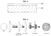
- FIG. 5 illustrates a method of manufacturing the hybrid structure of the silica nanoparticles-graphene quantum dots according to an example of the present disclosure.
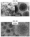
- FIGS. 6A and 6B show transmission electron microscope (TEM) images of the silica nanoparticles (SNPs) and the graphene quantum dots (GQDs) manufactured according to an example of the present disclosure.
- FIG. 7A shows TEM images of the silica nanoparticles, the graphene quantum dots, and the hybrid structure of the silica nanoparticles-graphene quantum dots.
- FIG. 7B shows a high-resolution (HR) TEM image of a surface of the hybrid structure of the silica nanoparticles-graphene quantum dots.
- HR high-resolution
- the silica nanoparticles are first manufactured.
- the silica nanoparticles (SNPs) may be manufactured using the Stöber process.
- the silica nanoparticles are formed through a process in which a silica precursor, tetraethyl orthosilicate (TEOS), is hydrolyzed with an aqueous alkaline solvent including an alkaline catalyst.
- TEOS tetraethyl orthosilicate
- ammonia water (NH 3 ), sodium hydroxide (NaOH), or the like may be used as a catalyst.
- the silica nanoparticles can be massively produced and can be manufactured to various diameters of 15 nm to 800 nm.
- silica nanoparticles (SNPs) manufactured through the process have a uniform size and a spherical shape.
- the graphene quantum dots are manufactured from a graphene oxide according to a hydrothermal method.
- a solution including the graphene quantum dots having various sizes was subjected to filtering and dialysis (dialysis) processes to classify the graphene quantum dots by size.
- Graphene quantum dots having an average size of 12 nm were selected.
- Quantum dots (GDQs) produced by this process are illustrated in FIG. 6B .
- the silica nanoparticles may be surface-treated before being combined with the graphene quantum dots (GQDs).
- This surface treatment may be performed as a pre-treatment for facilitating binding of the graphene quantum dots (GQDs) to surfaces of the silica nanoparticles (SNPs).
- the surface treatment was carried out as follows: NH 2 ligands were adsorbed to surfaces of the silica nanoparticles (SNPs) to positively charge the surfaces of the silica nanoparticles (SNPs), and then the silica nanoparticles (SNPs) were mixed with a 3 M HCl solution, followed by standing for nine hours.
- silica nanoparticles were incubated and dried in a 100 °C oven for three hours.
- the silica nanoparticles surface-treated with HCl were mixed with graphene quantum dots (GQDs) immersed in deionized water.
- An ammonium solution was added and mixed with the deionized water to adjust pH to 10, followed by allowing reaction therebetween in an ultrasonicator.
- GQDs negatively charged graphene quantum dots
- the graphene quantum dots have a two-dimensional planar shape and a plurality of the graphene quantum dots (GQDs) are immersed in deionized water. Accordingly, several graphene quantum dot fragments are bonded to and envelop a surface of a silica nanoparticle (SNP), as illustrated in FIG. 5 . In this case, the number of the graphene quantum dot fragments bonded to the surface of silica nanoparticle (SNP) may depend upon the surface area of the silica nanoparticle (SNP).
- the graphene quantum dots (GQDs) are bonded to a surface of the silica nanoparticle (SNP), whereby a clean and smooth silica nanoparticle (SNP) surface before binding becomes tough after binding.
- a crystalline pattern is observed. Accordingly, it can be confirmed that the graphene quantum dots (GQDs) are bonded to surfaces of the silica nanoparticles (SNPs).
- an energy conversion layer 230 having the hybrid structure of silica nanoparticles (SNPs)-graphene quantum dots (GQDs) manufactured by the process shown in FIG. 5 is transferred onto a first electrode 220 shown in FIG. 4 .
- a second electrode 240 is formed on the energy conversion layer 230 to manufacture a photoelectronic device.
- the second electrode 240 may be formed by the grapheme transfer method as in the first electrode 220.
- a contact electrode (not shown) may be disposed on each of the first and second electrodes 220 and 240.
- the contact electrode may be formed by sequentially depositing chrome/gold (Cr/Au) on each of the first and second electrodes 220 and 240.
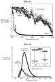
- FIG. 10 illustrates electron energy loss spectra (EELS) of silica nanoparticles (SNPs), graphene quantum dots (GQDs), and a hybrid structure of silica nanoparticles (SNPs)/graphene quantum dots (GQDs) according to an example of the present disclosure.
- EELS electron energy loss spectra
- silica nanoparticles SNPs
- O K-edge signals related to the silica nanoparticles SNPs
- GQDs graphene quantum dots
- both O K-edge signals related to the silica nanoparticles (SNPs) and the C K-edge signals related to the graphene quantum dots (GQDs) were observed. Due to the O K-edge and C K-edge signals, it can be confirmed that the hybrid structure includes the graphene quantum dots (GQDs) bonded to the silica nanoparticles (SNPs).
- FIGS. 11 to 17 illustrate graphs representing electrical/optical characteristics and energy transfer efficiency of a photoelectronic device including the hybrid structure of silica nanoparticles (SNPs)/graphene quantum dots (GQDs) according to the example of the present disclosure and materials or photoelectronic devices according to Comparative Examples 1 and 2, based on experimental data.
- SNPs silica nanoparticles
- GQDs graphene quantum dots
- the structures of the photoelectronic devices according to the example and the comparative examples are as follows.
- a photoelectronic device includes an energy conversion layer 130 or 230 having a hybrid structure of silica nanoparticles (SNPs)-graphene quantum dots (GQDs).
- SNPs silica nanoparticles
- GQDs graphene quantum dots
- the configuration of a photoelectronic device according to Comparative Example 1 is the same as that of the photoelectronic device illustrated in FIG. 1 or 9 , except that an energy conversion layer of the photoelectronic device is only composed of silica nanoparticles (indicated as "SNP” or “SNPs” on graphs).
- the configuration of a photoelectronic device according to Comparative Example 1 is the same as that of the photoelectronic device illustrated in FIG. 1 or 9 , except that an energy conversion layer of the photoelectronic device is only composed of graphene quantum dots (GQDs) (indicated as "GQDs" on graphs).
- GQDs graphene quantum dots
- FIG. 11 illustrates optical absorption spectra of photoelectronic devices according to Comparative Examples 1 and 2 and a photoelectronic device including a hybrid structure of silica nanoparticles (SNPs)/graphene quantum dots (GQDs) according to an example of the present disclosure.
- SNPs silica nanoparticles
- GQDs graphene quantum dots
- optical absorption occurred in a wavelength range of 200 nm to 1000 nm.
- optical absorption occurred near a wavelength of 250 nm.
- optical absorption occurred in a wavelength range of 200 nm to 1000 nm, which is similar to the optical absorption spectrum of Comparative Example 1. However, it can be confirmed that an optical absorption degree over the wavelength range of 200 nm to 1000 nm in the photoelectronic device according to the example is high, compared to Comparative Example 1.
- FIGS. 12 and 13 are photoluminescence (PL) and photoluminescence peak shift graphs of photoelectronic devices according to Comparative Examples 1 and 2 and a photoelectronic device including a hybrid structure of silica nanoparticles (SNPs)/graphene quantum dots (GQDs) according to an example of the present disclosure.
- SNPs silica nanoparticles
- GQDs graphene quantum dots
- the photoluminescence (PL) of the photoelectronic device according to Comparative Example 1 occurs in a wavelength range of 350 nm to 700 nm and the peak photoluminescence is observed at 382 nm (3.25 eV).
- the photoluminescence (PL) of the photoelectronic device according to Comparative Example 2 occurs in a wavelength range of 370 nm to 600 nm and the peak of the photoluminescence is observed at 414 nm (2.99 eV).
- the photoluminescence (PL) of the photoelectronic device according to the example occurs in a wavelength range of 350 nm to 700 nm and the peak of the photoluminescence is observed at 450 nm.
- the peak of the photoluminescence of the photoelectronic device according to the example is redshifted by about 36 nm, compared to that of the photoelectronic device according to Comparative Example 2.
- the photoluminescence of the photoelectronic device according to the example is much higher than that of Comparative Example 2. This can be considered to occur since a minimum energy level (S1) of the silica nanoparticles (SNPs) higher than that of the graphene quantum dots (GQDs) and thus energy transfer (ET) occurs from the silica nanoparticles (SNPs) to the graphene quantum dots (GQDs).
- S1 minimum energy level
- SNPs silica nanoparticles
- GQDs graphene quantum dots
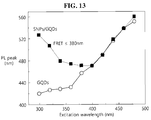
- FIG. 13 illustrates excitation light-photoluminescence peaks of the photoelectronic device according to each of Comparative Example 2 and the example.
- the photoluminescence peak gradually decreases while the wavelength of excitation light increases from 300 nm to 400 nm, and the photoluminescence peak gradually increases while the wavelength of excitation light increases from 400 nm to 480 nm.
- the photoluminescence peaks of the photoelectronic device according to Comparative Example 2 almost correspond with those of the example. This is considered to occur since electron-hole pairs cannot be generated in silica nanoparticles (SNPs) when the wavelength of excitation light is greater than 400 nm and thus energy transfer from the silica nanoparticles (SNPs) to the graphene quantum dots (GQDs) does not occur.
- SNPs silica nanoparticles
- GQDs graphene quantum dots
- FIGS. 14A and 14B are photoluminescence (PL) lifespan graphs of photoelectronic devices according to Comparative Examples 1 and 2 and a photoelectronic device including a hybrid structure of silica nanoparticles (SNPs)/graphene quantum dots (GQDs) according to an example of the present disclosure.
- SNPs silica nanoparticles
- GQDs graphene quantum dots
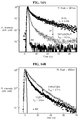
- FIG. 14A illustrates photoluminescence (PL) measured according to irradiation time of excitation light while irradiating the photoelectronic device of each of Comparative Example 1 and the example with excitation light having a wavelength of 305 nm.
- PL photoluminescence
- the PL lifespan of the photoelectronic device according to Comparative Example 1 is 2.3 ns ( ⁇ D ) and the PL lifespan of the photoelectronic device according to the example is -0.5 ns ( ⁇ DA ). Accordingly, it can be observed that the PL lifespa n of the photoelectronic device according to the example is decreased, compared to that of Comparative Example 1. This shows that electron-hole pairs which contributed to recombinati on in the silica nanoparticles (SNPs) are transferred to other energy levels.
- SNPs silica nanoparticles
- the PL lifespan of the photoelectronic device according to Comparative Example 2 is 1.6 ns ( ⁇ A ) and the PL lifespan of the photoelectronic device according to the example is 2.7 ns ( ⁇ AD ). Accordingly, it can be confirmed that the PL lifespa n of the photoelectronic device according to the example further increases, compared to that of Comparative Example 2.
- charge carriers in the silica nanoparticles are decreased due to energy transfer and the charge carriers transferred to the graphene quantum dots (GQDs) contribute to r adiative recombination of the graphene quantum dots (GQDs), thereby increasing the PL lifes pan of the graphene quantum dots (GQDs).
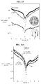
- FIG. 15 illustrates voltage-dark current curves of photoelectronic devices according to Comparative Examples 1 and 2 and a photoelectronic device including a hybrid structure of silica nanoparticles (SNPs)/graphene quantum dots (GQDs) according to an example of the present disclosure.
- SNPs silica nanoparticles
- GQDs graphene quantum dots
- the photoelectronic device according to Comparative Example 1 exhibits maximum current at a voltage of ⁇ 9 V.
- the maximum current is less than 10 -8 A/cm 2 .
- the photoelectronic device according to Comparative Example 2 exhibits a current of greater than 10 -5 A/cm 2 at a voltage of ⁇ 9 V and a current higher than that of Comparative Example 1 over the entire voltage in forward and backward directions.
- the photoelectronic device according to the example shows a current higher than those of Comparative Examples 1 and 2 over the entire voltage in forward and backward directions.
- the current in the photoelectronic device according to the example increases up to 10 4 to 10 5 folds ( ⁇ 10 4 folds at a voltage of less than 0 V and ⁇ 10 5 folds at a voltage of greater than 0 V).
- the graphene quantum dots (GQDs) are bonded to surfaces of the silica nanoparticles (SNPs), distances between the silica nanoparticles (SNPs) and the graphene quantum dots (GQDs) are greatly decreased. Accordingly, charge carriers generated on the surfaces of the silica nanoparticles (SNPs) can easily migrate to the graphene quantum dots ( GQDs) and thus current increases, whereby the measured current in the photoelectronic device according to the example is high. In addition, by adjusting the sizes of the graphene quantum dots (GQDs) or doping the graphene quantum dots (GQDs), the electrical characteristics of the photoelectronic device according to the example can be controlled.
- the photoelectronic device may be used as a light-emitting device.
- the aforementioned hybrid structure SNPs/GQDs
- the aforementioned hybrid structure is formed as a single or multiple layers between the electrodes included in the photoelectronic device, thereby increasing current density. Accordingly, light intensity may be controlled.
- the photoelectronic device according to the example may be used as a photosensor or a solar cell for generating photocurrent by irradiating light to an upper part of the photoelectronic device according to the example.
- FIGS. 16A to 16C illustrate voltage-current curves dependent upon incident light of photoelectronic devices according to Comparative Examples 1 and 2 and a photoelectronic device including a hybrid structure of silica nanoparticles (SNPs)/graphene quantum dots (GQDs) according to an example of the present disclosure.
- SNPs silica nanoparticles
- GQDs graphene quantum dots
- the photoelectronic device according to each of Comparative Examples 1 and 2 and the example has photoreaction to incident light and thus may be used as a solar cell or a photosensor, but the photoelectronic device according to the example exhibits satisfactory performance when used as a solar cell or a photosensor.
- FIGS. 17A and 17B illustrate graphs of light responsivity dependent upon voltage of photoelectronic devices according to Comparative Examples 1 and 2 and a photoelectronic device including a hybrid structure of silica nanoparticles (SNPs)/graphene quantum dots (GQDs) according to an example of the present disclosure.
- SNPs silica nanoparticles
- GQDs graphene quantum dots
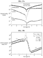
- FIG. 17A illustrates light responsivity measured by irradiating the photoelectronic devices with excitation light having a wavelength of 532 nm. From the drawing, it can be confirmed that the photoelectronic device according to Comparative Example 1 respectively represents ⁇ 7x10 -8 and ⁇ 8x10 -7 A/W at a voltage of ⁇ 5V and, accordingly, has low light responsivity. With regard to this, charge carriers are generated in the silica nanoparticles (SNPs) when light is radiated and the silica nanoparticles (SNPs) cannot smoothly transport the charge carriers, thereby exhibiting low responsivity to light.
- SNPs silica nanoparticles
- the photoelectronic device according to Comparative Example 2 respectively exhibits -0.31 and -0.007 A/W at a voltage of ⁇ 5V and has high light responsivity, compared to the photoelectronic device according to Comparative Example 1. This occurs because the electron-hole pairs generated in the graphene quantum dots (GQDs) migrate upon irradiation with light, thus contributing to current generation.
- GQDs graphene quantum dots
- the photoelectronic device according to the example has high light responsivity over the entire voltage in forward and backward directions, compared to the photoelectronic device according to Comparative Example 2.
- the order of light responsivity magnitudes in the photoelectronic devices of Comparative Examples 1 and 2 and the example when excitation light having another wavelength is radiated is as follows: Comparative Example 1 ⁇ Comparative Example2 ⁇ the example.
- FIG. 17B illustrates graphs representing the light responsivity (R Hybrid ) of the photoelectronic device according to the example relative to the light responsivity (R GQD ) of the photoelectronic device according to Comparative Example 2 (R Hybrid /R GQD ).
- R hybrid /R GQD when excitation light having a wavelength of 532 nm is radiated, R hybrid /R GQD is very great, i.e., 10 0 to 10 1 and 10 2 to 10 3 over the entire voltage in forward and backward directions.
- the photoelectronic device has a high light responsivity (R Hybrid ) of 0.93 to 4.14 A/W at a voltage area of -2V to -5V.
- This light responsivity is higher than the light responsivity ( ⁇ 0.5 A/W) of a commercialized photosensor made of silicon (Si) or the light responsivity (0.9 A/W) of a commercialized photosensor made of indium gallium arsenide.
- R hybrid /R GQD increases about two to three fold with respect to voltage in forward and backward directions, compared to when excitation light having a wavelength of 532 nm is radiated.
- silica nanoparticles SNPs
- GQDs graphene quantum dots
- the present disclosure provides an energy conversion layer in which graphene quantum dots are bonded to silica nanoparticles, thereby improving energy transfer efficiency between silica nanoparticles and graphene quantum dots.
Landscapes
- Chemical & Material Sciences (AREA)
- Organic Chemistry (AREA)
- Inorganic Chemistry (AREA)
- Engineering & Computer Science (AREA)
- Materials Engineering (AREA)
- Nanotechnology (AREA)
- Luminescent Compositions (AREA)
- Electroluminescent Light Sources (AREA)
- Manufacturing & Machinery (AREA)
- Led Device Packages (AREA)
Abstract
Description
- This application claims the priority benefit of Korean Patent Application No.
10-2015-0145614, filed on October 19, 2015 - The present disclosure relates to a photoelectronic device using a hybrid structure of silica nanoparticles and graphene quantum dots for increasing energy transfer efficiency by binding graphene quantum dots to silica nanoparticles and a method of manufacturing the same.
- Photoelectronic devices convert optical energy into electric energy or electric energy into optical energy. To increase such energy conversion efficiency, technology for using quantum dots in photoelectronic devices is being developed.
- Quantum dots, which are semiconductor nanoparticles with a diameter of several nanometers (nm), exhibit quantum mechanical characteristics such as quantum confinement. Such quantum dots autonomously release energy corresponding to their energy band gap upon entering an exited state by light from an excitation source. Since the energy band gap can be controlled by adjusting the sizes of the quantum dots, their electrical/optical characteristics can be also controlled. Accordingly, quantum dots can be applied to light-emitting devices, photoelectric conversion devices, or the like.
- Meanwhile, quantum dots can be densely arranged closely to each other such that energy transfer among quantum dots is facilitated. The electrical/optical characteristics of photoelectronic devices are improved with increasing energy transfer efficiency among quantum dots, and thus, research into increasing energy transfer efficiency is underway. However, even when quantum dots are densely arranged, the contact areas for transferring energy are small, thereby limiting increase in energy transfer efficiency. Therefore, there is a need for a method of increasing energy transfer efficiency among quantum dots.
-
- Korean Patent No.
10-0971197 (July 13, 2010 - Korean Patent Laid-Open Publication No.
2014-0134131 (November 21, 2014 - Korean Patent No.
10-1520804 (May 11, 2015 - Therefore, the present invention has been made in view of the above problems, and it is an object of the present invention to provide a photoelectronic device with a hybrid structure of silica nanoparticles and graphene quantum dots for increasing energy transfer efficiency by binding graphene quantum dots to silica nanoparticles and a method of manufacturing the same.
- In accordance with the present invention, the above and other objects can be accomplished by the provision of a photoelectronic device including a hybrid structure of silica nanoparticles-graphene quantum dots, wherein the photoelectronic device includes an energy conversion layer having a hybrid structure that includes graphene quantum dots (GODs) bonded to surfaces of silica nanoparticles (SNPs) and electrodes formed on upper and lower parts of the energy conversion layer.
- The silica nanoparticles may have spherical shapes, and the graphene quantum dots may have two-dimensional planar shapes and be bonded to surfaces of the spherical silica nanoparticles.
- The silica nanoparticles may be surface-treated for bonding to the graphene quantum dots.
- A method of manufacturing the photoelectronic device including the hybrid structure of the silica nanoparticles-graphene quantum dots includes: forming a first electrode on a substrate; forming an energy conversion layer having a hybrid structure of silica nanoparticles (SNPs) and graphene quantum dots (GODs) bonded to surfaces of the silica nanoparticles (SNPs) on the first electrode; and forming a second electrode on the energy conversion layer.
- The forming of the energy conversion layer may include: manufacturing the silica nanoparticles; manufacturing the graphene quantum dots; surface-treating the silica nanoparticles; and binding the graphene quantum dots to the surface-treated silica nanoparticles.
- The surface treating of the silica nanoparticles may include: adsorbing NH2 ligands to the silica nanoparticles to positively charge the surfaces of the silica nanoparticles; mixing the silica nanoparticles, to which the NH2 ligands are adsorbed, with an HCl solution; and drying the silica nanoparticles by filtering the HCl solution.
- The binding of the graphene quantum dots to the silica nanoparticles may include mixing the graphene quantum dots immersed in deionized water and the surface-treated silica nanoparticles and mixing an ammonium solution with the deionized water, followed by binding the graphene quantum dots to the surfaces of the silica nanoparticles by means of an ultrasonicator.
- The above and other objects, features and other advantages of the present invention will be more clearly understood from the following detailed description taken in conjunction with the accompanying drawings, in which:
-
FIG. 1 illustrates a photoelectronic device according to an example of the present disclosure; -
FIGS. 2 and 3 illustrate an energy transfer mechanism according to an example of the present disclosure; -
FIGS. 4 to 9 illustrate a method of manufacturing a photoelectronic device according to an example of the present disclosure; -
FIG. 10 illustrates electron energy loss spectra of silica nanoparticles (SNPs), graphene quantum dots (GQDs), and a hybrid structure of silica nanoparticles (SNPs)/graphene quantum dots (GQDs) according to an example of the present disclosure; -
FIG. 11 illustrates optical absorption spectra of photoelectronic devices according to Comparative Examples 1 and 2 and a photoelectronic device including a hybrid structure of silica nanoparticles (SNPs)/graphene quantum dots (GQDs) according to an example of the present disclosure; -
FIGS. 12 and13 are photoluminescence (PL) and photoluminescence peak shift graphs of photoelectronic devices according to Comparative Examples 1 and 2 and a photoelectronic device including a hybrid structure of silica nanoparticles (SNPs)/graphene quantum dots (GQDs) according to an example of the present disclosure; -
FIGS. 14A and 14B are photoluminescence (PL) lifespan graphs of photoelectronic devices according to Comparative Examples 1 and 2 and a photoelectronic device including a hybrid structure of silica nanoparticles (SNPs)/graphene quantum dots (GQDs) according to an example of the present disclosure; -
FIG. 15 illustrates voltage-dark current curves of photoelectronic devices according to Comparative Examples 1 and 2 and a photoelectronic device including a hybrid structure of silica nanoparticles (SNPs)/graphene quantum dots (GQDs) according to an example of the present disclosure; -
FIGS. 16A to 16C illustrate voltage-current curves dependent upon incident light of photoelectronic devices according to Comparative Examples 1 and 2 and a photoelectronic device including a hybrid structure of silica nanoparticles (SNPs)/graphene quantum dots (GQDs) according to an example of the present disclosure; and -
FIGS. 17A and 17B illustrate graphs of light responsivity dependent upon voltage of photoelectronic devices according to Comparative Examples 1 and 2 and a photoelectronic device including a hybrid structure of silica nanoparticles (SNPs)/graphene quantum dots (GQDs) according to an example of the present disclosure. - The present invention will now be described more fully with reference to the accompanying drawings and contents disclosed in the drawings. This invention may, however, be embodied in many different forms and should not be construed as limited to the exemplary embodiments set forth herein.
- When an element or a layer is referred to as being "on" another element or layer, the element or layer can be directly on another element or layer or an intervening element or layer can be present. On the other hand, when an element or layer is referred to as being "directly on" another element or layer, an intervening element or layer is not present.
- Spatially relative terms such as "below", "beneath", "lower", "above", or "upper" may be used herein to describe one element's relationship to another element as illustrated in the Figures. It will be understood that spatially relative terms are intended to encompass different orientations of the device in addition to the orientation depicted in the Figures. For example, if the device in one of the figures is turned over, elements described as "below" or "beneath" other elements would then be oriented "above" the other elements. The exemplary terms "below" or "beneath" can, therefore, encompass both an orientation of above and below. Since the device may be oriented in another direction, the spatially relative terms may be interpreted in accordance with the orientation of the device.
- The terminology used in the present disclosure is for the purpose of describing particular embodiments only and is not intended to limit the disclosure. As used in the disclosure and the appended claims, the singular forms "a", "an" and "the" are intended to include the plural forms as well, unless context clearly indicates otherwise. It will be further understood that the terms "comprises" and/or "comprising," when used in this specification, specify the presence of stated features, integers, steps, operations, elements, and/or components, but do not preclude the presence or addition of one or more other features, integers, steps, operations, elements, components, and/or groups thereof.
- Unless otherwise defined, all terms (including technical and scientific terms) used herein have the same meaning as commonly understood by one of ordinary skill in the art. It will be further understood that terms, such as those defined in commonly used dictionaries, should be interpreted as having a meaning that is consistent with their meaning in the context of the relevant art and the present disclosure, and will not be interpreted in an idealized or overly formal sense unless expressly so defined herein.
- Meanwhile, in the following description of the present invention, a detailed description of known functions and configurations incorporated herein will be omitted when it may make the subject matter of the present invention unclear. The terms used in the specification are employed to suitably express embodiments of the present invention, and can be changed according to the intention of clients or operators, practices in the art, or the like. Accordingly, definitions of the terms should be understood on the basis of the entire description of the present specification.
-
FIG. 1 illustrates a photoelectronic device according to an example of the present disclosure. - Referring to
FIG. 1 , aphotoelectronic device 100 according to an example of the present disclosure includes a hybrid structure of silica nanoparticles (SNPs)-graphene quantum dots (GQDs). In particular, thephotoelectronic device 100 includes thesubstrate 110, afirst electrode 120, anenergy conversion layer 130, and asecond electrode 140. - The
energy conversion layer 130 may have a hybrid structure wherein graphene quantum dots (GQDs) are bonded to surfaces of silica nanoparticles (SNPs). - Amorphous silica, SiO2, is very hard, thermally and chemically stable, and nontoxic, thus having attracted attention as a next-generation material for use in electronics. However, since silica has photophysical characteristics and is transparent, inactive, and hydrophilic, silica does not transfer energy or electrons. However, when silica is processed to micro or nano scale, silica can transfer energy or electrons and, without doping with a phosphor, has improved optical absorption in infrared, ultraviolet, and visible light bands and light-emitting characteristics.
- In addition, graphene quantum dots (GQDs) have superior optical absorption characteristics in ultraviolet and visible light bands and luminescence when exposed to ultraviolet and near-infrared light. Accordingly, graphene quantum dots (GQDs) can be used as energy donors or energy acceptors. In addition, graphene quantum dots (GQDs) have long light-emitting lifespan, high photostability, and a high quantum yield, and thus, can be applied to an energy transfer system.
- According to an example, in the
energy conversion layer 130, the silica nanoparticles (SNPs) function as energy donors and the graphene quantum dots (GQDs) function as energy acceptors and thus energy transfer occurs therebetween. That is, theenergy conversion layer 130 functions as an energy transfer system. - To increase energy transfer efficiency of the
energy conversion layer 130, an area to which energy is transferred, i.e., binding areas between silica nanoparticles (SNPs) and graphene quantum dots (GQDs), is preferably wide. - According to the example, the silica nanoparticles (SNPs) are spherical shapes and the graphene quantum dots (GQDs) have two-dimensional planar shapes. Several graphene quantum dot fragments may bind to a silica nanoparticle by enveloping the entire surface of the silica nanoparticle.
- In addition, to improve binding force between the silica nanoparticles (SNPs) and the graphene quantum dots (GQDs), the silica nanoparticles (SNPs) may be surface-treated. A particular surface treatment method is described below.
-
FIGS. 2 and 3 illustrate an energy transfer mechanism according to an example of the present disclosure. Referring toFIGS. 2 and 3 , when light is radiated to the hybrid structure wherein the graphene quantum dots (GQDs) are bonded to the surfaces of the silica nanoparticles (SNPs), interaction between the silica nanoparticles (SNPs) and the graphene quantum dots (GQDs) occurs. - In particular, when light is radiated, the light is absorbed by the silica nanoparticles (SNPs) and thus electron-hole pairs (+, -) are generated on the surfaces of the silica nanoparticles. Here, some electron-hole pairs are emitted as heat and lost. The remaining electron-hole pairs emit light via a recombination process. In this process, energy transfer between the silica nanoparticles (SNPs) and the graphene quantum dots (GQDs) bonded to SNPs occurs.
- Since the minimum energy levels (S1) of the silica nanoparticles (SNPs) are higher than those of the graphene quantum dots (GQDs), energy transfer occurs from the silica nanoparticles (SNPs) to the graphene quantum dots (GQDs). That is, the silica nanoparticles (SNPs) function as energy donors and the graphene quantum dots (GQDs) function as energy acceptors.
- When light is radiated, most electron-hole pairs are formed on surfaces of the silica nanoparticles (SNPs), and thus, distances (R0) between the silica nanoparticles (SNPs) and the graphene quantum dots (GQDs) are shortened, whereby energy transfer is facilitated. In the example of the present invention, the graphene quantum dots (GQDs) are bonded to the silica nanoparticles (SNPs) in a form of enveloping the entire surfaces of the silica nanoparticles (SNPs), thereby increasing energy transfer efficiency of the hybrid structure. When energy transfer efficiency increases, light emission and current flow in graphene quantum dots (GQDs) can increase.
-
FIGS. 4 to 9 illustrate a method of manufacturing a photoelectronic device according to an example of the present disclosure. - To manufacture a photoelectronic device, graphene is first transferred on a
substrate 210 to form afirst electrode 220, as illustrated inFIG. 4 . Thesubstrate 210 may be a SiO2 or Si substrate. In addition, thesubstrate 210 may be a hard substrate, such as a gallium arsenide, silicon germanium, ceramic, or quartz substrate or a glass substrate for display, or a fusible plastic substrate, such as polyimide, polyethylene terephthalate (PET), polyethylene naphthalate (PEN), poly(methyl methacrylate) (PMMA), polycarbonate (PC), polyethersulfone (PES), or polyester). However, thesubstrate 210 is not limited to the substrate types and may be other substrates having optical transparency allowing penetration of light. -
FIG. 5 illustrates a method of manufacturing the hybrid structure of the silica nanoparticles-graphene quantum dots according to an example of the present disclosure.FIGS. 6A and 6B show transmission electron microscope (TEM) images of the silica nanoparticles (SNPs) and the graphene quantum dots (GQDs) manufactured according to an example of the present disclosure. In addition,FIG. 7A shows TEM images of the silica nanoparticles, the graphene quantum dots, and the hybrid structure of the silica nanoparticles-graphene quantum dots.FIG. 7B shows a high-resolution (HR) TEM image of a surface of the hybrid structure of the silica nanoparticles-graphene quantum dots. - Referring to
FIG. 5 , the silica nanoparticles (SNPs) are first manufactured. The silica nanoparticles (SNPs) may be manufactured using the Stöber process. In particular, the silica nanoparticles are formed through a process in which a silica precursor, tetraethyl orthosilicate (TEOS), is hydrolyzed with an aqueous alkaline solvent including an alkaline catalyst. Here, ammonia water (NH3), sodium hydroxide (NaOH), or the like may be used as a catalyst. - By using the Stöber process, the silica nanoparticles (SNPs) can be massively produced and can be manufactured to various diameters of 15 nm to 800 nm.
- As illustrated in
FIG. 6A , it can be confirmed that silica nanoparticles (SNPs) manufactured through the process have a uniform size and a spherical shape. - The graphene quantum dots are manufactured from a graphene oxide according to a hydrothermal method. A solution including the graphene quantum dots having various sizes was subjected to filtering and dialysis (dialysis) processes to classify the graphene quantum dots by size. Graphene quantum dots having an average size of 12 nm were selected. Quantum dots (GDQs) produced by this process are illustrated in
FIG. 6B . - Meanwhile, the silica nanoparticles (SNPs) may be surface-treated before being combined with the graphene quantum dots (GQDs). This surface treatment may be performed as a pre-treatment for facilitating binding of the graphene quantum dots (GQDs) to surfaces of the silica nanoparticles (SNPs).
- The surface treatment was carried out as follows: NH2 ligands were adsorbed to surfaces of the silica nanoparticles (SNPs) to positively charge the surfaces of the silica nanoparticles (SNPs), and then the silica nanoparticles (SNPs) were mixed with a 3 M HCl solution, followed by standing for nine hours.
- Subsequently, filtering was carried out with HCl and the silica nanoparticles were incubated and dried in a 100 °C oven for three hours. The silica nanoparticles surface-treated with HCl were mixed with graphene quantum dots (GQDs) immersed in deionized water. An ammonium solution was added and mixed with the deionized water to adjust pH to 10, followed by allowing reaction therebetween in an ultrasonicator.
- By this process, negatively charged graphene quantum dots (GQDs) are strongly bonded to the NH2 ligands adsorbed to surfaces of the silica nanoparticles (SNPs).
- The graphene quantum dots (GQDs) have a two-dimensional planar shape and a plurality of the graphene quantum dots (GQDs) are immersed in deionized water. Accordingly, several graphene quantum dot fragments are bonded to and envelop a surface of a silica nanoparticle (SNP), as illustrated in
FIG. 5 . In this case, the number of the graphene quantum dot fragments bonded to the surface of silica nanoparticle (SNP) may depend upon the surface area of the silica nanoparticle (SNP). - Referring to
FIG. 7A , it can be observed that the graphene quantum dots (GQDs) are bonded to a surface of the silica nanoparticle (SNP), whereby a clean and smooth silica nanoparticle (SNP) surface before binding becomes tough after binding. In addition, as illustrated in the HR-TEM image ofFIG. 7B , a crystalline pattern is observed. Accordingly, it can be confirmed that the graphene quantum dots (GQDs) are bonded to surfaces of the silica nanoparticles (SNPs). - As illustrated in
FIG. 8 , anenergy conversion layer 230 having the hybrid structure of silica nanoparticles (SNPs)-graphene quantum dots (GQDs) manufactured by the process shown inFIG. 5 is transferred onto afirst electrode 220 shown inFIG. 4 . Subsequently, asecond electrode 240 is formed on theenergy conversion layer 230 to manufacture a photoelectronic device. Thesecond electrode 240 may be formed by the grapheme transfer method as in thefirst electrode 220. - Although not shown in the drawings, a contact electrode (not shown) may be disposed on each of the first and
second electrodes second electrodes -
FIG. 10 illustrates electron energy loss spectra (EELS) of silica nanoparticles (SNPs), graphene quantum dots (GQDs), and a hybrid structure of silica nanoparticles (SNPs)/graphene quantum dots (GQDs) according to an example of the present disclosure. - In the silica nanoparticles (SNPs), only O K-edge signals related to the silica nanoparticles (SNPs) were observed and, in the graphene quantum dots (GQDs), only C K-edge signals related to the graphene quantum dots (GQDs) were observed.
- On the other hand, in the hybrid structure according to the example of the present invention, both O K-edge signals related to the silica nanoparticles (SNPs) and the C K-edge signals related to the graphene quantum dots (GQDs) were observed. Due to the O K-edge and C K-edge signals, it can be confirmed that the hybrid structure includes the graphene quantum dots (GQDs) bonded to the silica nanoparticles (SNPs).
-
FIGS. 11 to 17 illustrate graphs representing electrical/optical characteristics and energy transfer efficiency of a photoelectronic device including the hybrid structure of silica nanoparticles (SNPs)/graphene quantum dots (GQDs) according to the example of the present disclosure and materials or photoelectronic devices according to Comparative Examples 1 and 2, based on experimental data. Here, the structures of the photoelectronic devices according to the example and the comparative examples are as follows. - As illustrated in
FIG. 1 or9 , a photoelectronic device according to the present disclosure includes anenergy conversion layer - The configuration of a photoelectronic device according to Comparative Example 1 is the same as that of the photoelectronic device illustrated in
FIG. 1 or9 , except that an energy conversion layer of the photoelectronic device is only composed of silica nanoparticles (indicated as "SNP" or "SNPs" on graphs). - The configuration of a photoelectronic device according to Comparative Example 1 is the same as that of the photoelectronic device illustrated in
FIG. 1 or9 , except that an energy conversion layer of the photoelectronic device is only composed of graphene quantum dots (GQDs) (indicated as "GQDs" on graphs). -
FIG. 11 illustrates optical absorption spectra of photoelectronic devices according to Comparative Examples 1 and 2 and a photoelectronic device including a hybrid structure of silica nanoparticles (SNPs)/graphene quantum dots (GQDs) according to an example of the present disclosure. - In the photoelectronic device according to Comparative Example 1, optical absorption occurred in a wavelength range of 200 nm to 1000 nm. In the photoelectronic device according to Comparative Example 2, optical absorption occurred near a wavelength of 250 nm.
- In the photoelectronic device according to the example, optical absorption occurred in a wavelength range of 200 nm to 1000 nm, which is similar to the optical absorption spectrum of Comparative Example 1. However, it can be confirmed that an optical absorption degree over the wavelength range of 200 nm to 1000 nm in the photoelectronic device according to the example is high, compared to Comparative Example 1.
- This occurs due to mix of optical absorption by the silica nanoparticles (SNPs) and optical absorption by the graphene quantum dots (GQDs). That is, it can be confirmed that an optical absorption ratio increases due to the hybrid structure of the silica nanoparticles (SNPs)-graphene quantum dots (GQDs).
-
FIGS. 12 and13 are photoluminescence (PL) and photoluminescence peak shift graphs of photoelectronic devices according to Comparative Examples 1 and 2 and a photoelectronic device including a hybrid structure of silica nanoparticles (SNPs)/graphene quantum dots (GQDs) according to an example of the present disclosure. - Referring to
FIG. 12 , the photoluminescence (PL) of the photoelectronic device according to Comparative Example 1 occurs in a wavelength range of 350 nm to 700 nm and the peak photoluminescence is observed at 382 nm (3.25 eV). - In addition, the photoluminescence (PL) of the photoelectronic device according to Comparative Example 2 occurs in a wavelength range of 370 nm to 600 nm and the peak of the photoluminescence is observed at 414 nm (2.99 eV).
- The photoluminescence (PL) of the photoelectronic device according to the example occurs in a wavelength range of 350 nm to 700 nm and the peak of the photoluminescence is observed at 450 nm.
- Meanwhile, the peak of the photoluminescence of the photoelectronic device according to the example is redshifted by about 36 nm, compared to that of the photoelectronic device according to Comparative Example 2. Simultaneously, the photoluminescence of the photoelectronic device according to the example is much higher than that of Comparative Example 2. This can be considered to occur since a minimum energy level (S1) of the silica nanoparticles (SNPs) higher than that of the graphene quantum dots (GQDs) and thus energy transfer (ET) occurs from the silica nanoparticles (SNPs) to the graphene quantum dots (GQDs).
-
FIG. 13 illustrates excitation light-photoluminescence peaks of the photoelectronic device according to each of Comparative Example 2 and the example. - In the case of the photoelectronic device according to Comparative Example 2, when the wavelength of excitation light increases from 300 nm to 480 nm, the photoluminescence peak is redshifted from 421 nm to 551 nm, which is similar to a general photoluminescence peak shift phenomenon in graphene quantum dots (GQDs).
- On the other hand, in the case of the photoelectronic device according to the example, the photoluminescence peak gradually decreases while the wavelength of excitation light increases from 300 nm to 400 nm, and the photoluminescence peak gradually increases while the wavelength of excitation light increases from 400 nm to 480 nm.
- Meanwhile, when the wavelength of excitation light is greater than 400 nm, the photoluminescence peaks of the photoelectronic device according to Comparative Example 2 almost correspond with those of the example. This is considered to occur since electron-hole pairs cannot be generated in silica nanoparticles (SNPs) when the wavelength of excitation light is greater than 400 nm and thus energy transfer from the silica nanoparticles (SNPs) to the graphene quantum dots (GQDs) does not occur.
- On the other hand, electron-hole pair are generated in the silica nanoparticles (SNPs) when the wavelength of excitation light is less than 400 nm and thus energy transfer to graphen e quantum dots (GQDs) occurs. Accordingly, in the photoelectronic device according to the example, PL peaks are exhibited at longer wavelength, compared to Comparative Example 2.
-
FIGS. 14A and 14B are photoluminescence (PL) lifespan graphs of photoelectronic devices according to Comparative Examples 1 and 2 and a photoelectronic device including a hybrid structure of silica nanoparticles (SNPs)/graphene quantum dots (GQDs) according to an example of the present disclosure. -
FIG. 14A illustrates photoluminescence (PL) measured according to irradiation time of excitation light while irradiating the photoelectronic device of each of Comparative Example 1 and the example with excitation light having a wavelength of 305 nm. In particular, a PL decay curve with respect to an energy donor is illustrated in each of the photoelectronic devices. - Referring to
FIG. 14A , the PL lifespan of the photoelectronic device according to Comparative Example 1 is 2.3 ns (τD) and the PL lifespan of the photoelectronic device according to the example is -0.5 ns (τDA). Accordingly, it can be observed that the PL lifespa n of the photoelectronic device according to the example is decreased, compared to that of Comparative Example 1. This shows that electron-hole pairs which contributed to recombinati on in the silica nanoparticles (SNPs) are transferred to other energy levels. - Referring to
FIG. 14B , the PL lifespan of the photoelectronic device according to Comparative Example 2 is 1.6 ns (τA) and the PL lifespan of the photoelectronic device according to the example is 2.7 ns (τAD). Accordingly, it can be confirmed that the PL lifespa n of the photoelectronic device according to the example further increases, compared to that of Comparative Example 2. - That is, charge carriers in the silica nanoparticles (SNPs) are decreased due to energy transfer and the charge carriers transferred to the graphene quantum dots (GQDs) contribute to r adiative recombination of the graphene quantum dots (GQDs), thereby increasing the PL lifes pan of the graphene quantum dots (GQDs).
-
FIG. 15 illustrates voltage-dark current curves of photoelectronic devices according to Comparative Examples 1 and 2 and a photoelectronic device including a hybrid structure of silica nanoparticles (SNPs)/graphene quantum dots (GQDs) according to an example of the present disclosure. - Voltage was applied to two electrodes included in the photoelectronic device of each of Comparative Examples 1 and 2 and the example and dark current was measured.
- Referring to
FIG. 15 , the photoelectronic device according to Comparative Example 1 exhibits maximum current at a voltage of ± 9 V. The maximum current is less than 10-8 A/cm2. In addition, the photoelectronic device according to Comparative Example 2 exhibits a current of greater than 10-5 A/cm2 at a voltage of ±9 V and a current higher than that of Comparative Example 1 over the entire voltage in forward and backward directions. - Meanwhile, the photoelectronic device according to the example shows a current higher than those of Comparative Examples 1 and 2 over the entire voltage in forward and backward directions. In particular, when compared to Comparative Example 1, the current in the photoelectronic device according to the example increases up to 104 to 105 folds (∼ 104 folds at a voltage of less than 0 V and ∼ 105 folds at a voltage of greater than 0 V).
- When the graphene quantum dots (GQDs) are bonded to surfaces of the silica nanoparticles (SNPs), distances between the silica nanoparticles (SNPs) and the graphene quantum dots (GQDs) are greatly decreased. Accordingly, charge carriers generated on the surfaces of the silica nanoparticles (SNPs) can easily migrate to the graphene quantum dots ( GQDs) and thus current increases, whereby the measured current in the photoelectronic device according to the example is high. In addition, by adjusting the sizes of the graphene quantum dots (GQDs) or doping the graphene quantum dots (GQDs), the electrical characteristics of the photoelectronic device according to the example can be controlled.
- Meanwhile, by increasing current density through voltage application to the photoelectronic device according to the example, the photoelectronic device may be used as a light-emitting device. In this case, the aforementioned hybrid structure (SNPs/GQDs) is formed as a single or multiple layers between the electrodes included in the photoelectronic device, thereby increasing current density. Accordingly, light intensity may be controlled.
- In addition, the photoelectronic device according to the example may be used as a photosensor or a solar cell for generating photocurrent by irradiating light to an upper part of the photoelectronic device according to the example.
-
FIGS. 16A to 16C illustrate voltage-current curves dependent upon incident light of photoelectronic devices according to Comparative Examples 1 and 2 and a photoelectronic device including a hybrid structure of silica nanoparticles (SNPs)/graphene quantum dots (GQDs) according to an example of the present disclosure. - Currents dependent upon voltages were measured while irradiating excitation light with a wavelength of each of 325 nm and 532 nm to an upper part of the photoelectronic device of each of Comparative Examples 1 and 2 and the example.
- Referring to
FIGS. 16A and16B , it can be confirmed that, when excitation light having a wavelength of 325 nm or 532 nm is radiated to the photoelectronic device according to each of Comparative Examples 1 and 2, current is generated dependently upon voltage, compared to the cases in which light is not radiated (dark). - In addition, referring to
FIG. 16C , it also can be confirmed that, when excitation light having a wavelength of 325 nm or 532 nm is radiated to the photoelectronic device according to the example, current is generated dependently upon voltage, compared to the cases in which light is not radiated (dark). - Further, it can be confirmed that currents dependent upon voltages in the photoelectronic device according to the example are higher than those in the photoelectronic devices according to Comparative Examples 1 and 2, and, when excitation light with a wavelength of 325 nm or 532 nm is radiated, currents in the photoelectronic device according to the example are almost the same as those in Comparative Examples 1 and 2.
- When these are considered, it can be confirmed that the photoelectronic device according to each of Comparative Examples 1 and 2 and the example has photoreaction to incident light and thus may be used as a solar cell or a photosensor, but the photoelectronic device according to the example exhibits satisfactory performance when used as a solar cell or a photosensor.
-
FIGS. 17A and 17B illustrate graphs of light responsivity dependent upon voltage of photoelectronic devices according to Comparative Examples 1 and 2 and a photoelectronic device including a hybrid structure of silica nanoparticles (SNPs)/graphene quantum dots (GQDs) according to an example of the present disclosure. -
FIG. 17A illustrates light responsivity measured by irradiating the photoelectronic devices with excitation light having a wavelength of 532 nm. From the drawing, it can be confirmed that the photoelectronic device according to Comparative Example 1 respectively represents ∼7x10⁻⁸ and ∼8x10⁻⁷ A/W at a voltage of ± 5V and, accordingly, has low light responsivity. With regard to this, charge carriers are generated in the silica nanoparticles (SNPs) when light is radiated and the silica nanoparticles (SNPs) cannot smoothly transport the charge carriers, thereby exhibiting low responsivity to light. - On the other hand, the photoelectronic device according to Comparative Example 2 respectively exhibits -0.31 and -0.007 A/W at a voltage of ± 5V and has high light responsivity, compared to the photoelectronic device according to Comparative Example 1. This occurs because the electron-hole pairs generated in the graphene quantum dots (GQDs) migrate upon irradiation with light, thus contributing to current generation.
- Meanwhile, the photoelectronic device according to the example has high light responsivity over the entire voltage in forward and backward directions, compared to the photoelectronic device according to Comparative Example 2. Although not shown in the graphs, the order of light responsivity magnitudes in the photoelectronic devices of Comparative Examples 1 and 2 and the example when excitation light having another wavelength is radiated is as follows: Comparative Example 1<Comparative Example2<the example.
-
FIG. 17B illustrates graphs representing the light responsivity (RHybrid) of the photoelectronic device according to the example relative to the light responsivity (RGQD) of the photoelectronic device according to Comparative Example 2 (RHybrid/RGQD). - Referring to
FIG. 17B , when excitation light having a wavelength of 532 nm is radiated, Rhybrid/RGQD is very great, i.e., 100 to 101 and 102 to 103 over the entire voltage in forward and backward directions. - In particular, the photoelectronic device according to the example has a high light responsivity (RHybrid) of 0.93 to 4.14 A/W at a voltage area of -2V to -5V. This light responsivity is higher than the light responsivity (∼0.5 A/W) of a commercialized photosensor made of silicon (Si) or the light responsivity (0.9 A/W) of a commercialized photosensor made of indium gallium arsenide.
- This occurs because the charge carriers generated on the surfaces of the silica nanoparticles (SNPs) due to optical absorption in the photoelectronic device according to the example are transferred to the graphene quantum dots (GQDs) bonded to the surfaces of the silica nanoparticles (SNPs) and thus energy transfer occurs.
- In addition, when excitation light having a wavelength of 325 nm is radiated, Rhybrid/RGQD increases about two to three fold with respect to voltage in forward and backward directions, compared to when excitation light having a wavelength of 532 nm is radiated.
- This can be considered to occur because the silica nanoparticles (SNPs) have a higher optical absorption degree at a wavelength of 325 nm than at a wavelength of 532 nm and thus more charge carriers are transferred to the graphene quantum dots (GQDs), as in the energy transfer results shown as the optical absorption degree and the photoluminescence.
- As described above, the present disclosure provides an energy conversion layer in which graphene quantum dots are bonded to silica nanoparticles, thereby improving energy transfer efficiency between silica nanoparticles and graphene quantum dots.
- Although the preferred embodiments of the present invention have been disclosed with reference to limited examples and drawings, those skilled in the art will appreciate that various modifications, additions and substitutions are possible, without departing from the scope and spirit of the invention. For example, although the described technologies can be performed in an order different from the order of the described methods and/or the described systems, structures, apparatuses, circuits, etc. are coupled or combined in forms different from the described methods or substituted with other constituents or equivalents, suitable outcomes can be accomplished.
- Therefore, it should be understood that the scope of the appended claims include other embodiments and examples and the equivalents of the claims.
Claims (7)
- A photoelectronic device, comprising:an energy conversion layer having a hybrid structure that comprises graphene quantum dots (GODs) bonded to surfaces of silica nanoparticles (SNPs); andelectrodes formed on an upper and lower parts of the energy conversion layer.
- The photoelectronic device according to claim 1, wherein the silica nanoparticles have spherical shapes, and
the graphene quantum dots have two-dimensional planar shapes and be bonded to surfaces of the spherical shapes. - The photoelectronic device according to claim 1, wherein the silica nanoparticles are surface-treated to be bonded with the graphene quantum dots.
- A method of manufacturing a photoelectronic device substrate, the method comprising:forming a first electrode on a substrate;forming an energy conversion layer having a hybrid structure of silica nanoparticles (SNPs) and graphene quantum dots (GODs) bonded to surfaces of silica nanoparticles (SNPs) on the first electrode; andforming a second electrode on the energy conversion layer.
- The method according to claim 4, wherein the forming of the energy conversion layer comprises:manufacturing the silica nanoparticles;manufacturing the graphene quantum dots;surface-treating the silica nanoparticles; andbinding the graphene quantum dots to the surface-treated silica nanoparticles.
- The method according to claim 5, wherein the surface treating comprises:adsorbing NH2 ligands to the silica nanoparticles to positively charge the surfaces of the silica nanoparticles;mixing the silica nanoparticles, to which the NH2 ligands are adsorbed, with a HCl solution; anddrying the silica nanoparticles by filtering the HCl solution.
- The method according to claim 5, wherein the binding comprises mixing the graphene quantum dots immersed in deionized water and the surface-treated silica nanoparticles and mixing an ammonium solution with the deionized water, followed by binding the graphene quantum dots to the surfaces of the silica nanoparticles by means of an ultrasonicator.
Applications Claiming Priority (1)
| Application Number | Priority Date | Filing Date | Title |
|---|---|---|---|
| KR1020150145614A KR101714904B1 (en) | 2015-10-19 | 2015-10-19 | Photoelectronic device using hybrid structure of silica nano particles-graphene quantum dots and method of manufacturing the same |
Publications (2)
| Publication Number | Publication Date |
|---|---|
| EP3159944A1 true EP3159944A1 (en) | 2017-04-26 |
| EP3159944B1 EP3159944B1 (en) | 2019-08-07 |
Family
ID=56936236
Family Applications (1)
| Application Number | Title | Priority Date | Filing Date |
|---|---|---|---|
| EP16178407.9A Active EP3159944B1 (en) | 2015-10-19 | 2016-07-07 | Photoelectronic device using hybrid structure of silica nanoparticles-graphene quantum dots and method of manufacturing the same |
Country Status (3)
| Country | Link |
|---|---|
| US (1) | US9755093B2 (en) |
| EP (1) | EP3159944B1 (en) |
| KR (1) | KR101714904B1 (en) |
Cited By (1)
| Publication number | Priority date | Publication date | Assignee | Title |
|---|---|---|---|---|
| CN112242469A (en) * | 2020-10-22 | 2021-01-19 | 中国科学院长春光学精密机械与物理研究所 | Graphene electrode-based vertical-structure deep ultraviolet LED and preparation method thereof |
Families Citing this family (3)
| Publication number | Priority date | Publication date | Assignee | Title |
|---|---|---|---|---|
| TWI593134B (en) * | 2016-05-19 | 2017-07-21 | Method and structure for manufacturing graphene quantum dot on light-emitting diode | |
| CN110964499A (en) * | 2018-09-30 | 2020-04-07 | Tcl集团股份有限公司 | Composite material and preparation method and application thereof |
| CN114823950B (en) * | 2022-05-10 | 2024-06-07 | 云南师范大学 | A photodetector based on carbon quantum dots and noble metal nanoparticles |
Citations (8)
| Publication number | Priority date | Publication date | Assignee | Title |
|---|---|---|---|---|
| KR100971197B1 (en) | 2008-09-26 | 2010-07-20 | 한국기계연구원 | Quantum dot having improved electron transporting performance and method for manufacturing thereof |
| KR20130038428A (en) * | 2011-10-07 | 2013-04-18 | 한국과학기술연구원 | Metal oxide semiconductor-nanocarbon consolidated core-shell quantum dots and ultraviolet photovoltaic cell using it and a fabrication process thereof |
| KR101421064B1 (en) * | 2013-04-01 | 2014-07-18 | 국립대학법인 울산과학기술대학교 산학협력단 | Hydrophobic nano-graphene laminate and method for preparing same |
| CN102709399B (en) * | 2012-06-21 | 2014-10-15 | 上海理工大学 | Manufacturing method of high-efficiency nano antenna solar battery |
| KR20140134131A (en) | 2013-05-13 | 2014-11-21 | 경희대학교 산학협력단 | Graphene quantum dot phtodetector and the Fabricating Method thereof |
| KR20150014557A (en) * | 2013-07-29 | 2015-02-09 | 이화여자대학교 산학협력단 | Carbon-metal oxide hybrid nanostructure, preparing method of the same, photoelectrode including the same, and dye-sensitized solar cell including the photoelectrode |
| KR101520804B1 (en) | 2013-01-30 | 2015-05-15 | 한국표준과학연구원 | High-efficient Solar Cell using wide-band absorption and energy transfer |
| KR101558801B1 (en) * | 2014-08-21 | 2015-10-12 | 경희대학교 산학협력단 | Photo diode using hybrid structure of graphene-silicon quantum dots and method of manufacturing the same |
Family Cites Families (6)
| Publication number | Priority date | Publication date | Assignee | Title |
|---|---|---|---|---|
| TW201032340A (en) * | 2009-02-26 | 2010-09-01 | Nat Applied Res Laboratories | A silicon quantum dot near-infrared phototransistor detector |
| WO2011008064A2 (en) * | 2009-07-17 | 2011-01-20 | 서울대학교 산학협력단 | Particles containing quantum dot and method for producing same |
| KR101286106B1 (en) * | 2011-05-30 | 2013-07-16 | 한국과학기술연구원 | The method for producing graphene by chemical exfoliation |
| US9443998B2 (en) * | 2013-03-14 | 2016-09-13 | Nanoco Technologies Ltd. | Multi-layer-coated quantum dot beads |
| KR101534313B1 (en) * | 2014-08-04 | 2015-07-06 | 성균관대학교산학협력단 | Electrochromic device including carbon-based material and viologen-based compound, and method for producing the same |
| WO2016125189A1 (en) * | 2015-02-03 | 2016-08-11 | Council Of Scientific & Industrial Research | Novel composite of silica and graphene quantum dots and preparation thereof |
-
2015
- 2015-10-19 KR KR1020150145614A patent/KR101714904B1/en active Active
-
2016
- 2016-07-07 EP EP16178407.9A patent/EP3159944B1/en active Active
- 2016-07-13 US US15/208,768 patent/US9755093B2/en active Active
Patent Citations (8)
| Publication number | Priority date | Publication date | Assignee | Title |
|---|---|---|---|---|
| KR100971197B1 (en) | 2008-09-26 | 2010-07-20 | 한국기계연구원 | Quantum dot having improved electron transporting performance and method for manufacturing thereof |
| KR20130038428A (en) * | 2011-10-07 | 2013-04-18 | 한국과학기술연구원 | Metal oxide semiconductor-nanocarbon consolidated core-shell quantum dots and ultraviolet photovoltaic cell using it and a fabrication process thereof |
| CN102709399B (en) * | 2012-06-21 | 2014-10-15 | 上海理工大学 | Manufacturing method of high-efficiency nano antenna solar battery |
| KR101520804B1 (en) | 2013-01-30 | 2015-05-15 | 한국표준과학연구원 | High-efficient Solar Cell using wide-band absorption and energy transfer |
| KR101421064B1 (en) * | 2013-04-01 | 2014-07-18 | 국립대학법인 울산과학기술대학교 산학협력단 | Hydrophobic nano-graphene laminate and method for preparing same |
| KR20140134131A (en) | 2013-05-13 | 2014-11-21 | 경희대학교 산학협력단 | Graphene quantum dot phtodetector and the Fabricating Method thereof |
| KR20150014557A (en) * | 2013-07-29 | 2015-02-09 | 이화여자대학교 산학협력단 | Carbon-metal oxide hybrid nanostructure, preparing method of the same, photoelectrode including the same, and dye-sensitized solar cell including the photoelectrode |
| KR101558801B1 (en) * | 2014-08-21 | 2015-10-12 | 경희대학교 산학협력단 | Photo diode using hybrid structure of graphene-silicon quantum dots and method of manufacturing the same |
Cited By (1)
| Publication number | Priority date | Publication date | Assignee | Title |
|---|---|---|---|---|
| CN112242469A (en) * | 2020-10-22 | 2021-01-19 | 中国科学院长春光学精密机械与物理研究所 | Graphene electrode-based vertical-structure deep ultraviolet LED and preparation method thereof |
Also Published As
| Publication number | Publication date |
|---|---|
| US20170110609A1 (en) | 2017-04-20 |
| EP3159944B1 (en) | 2019-08-07 |
| US9755093B2 (en) | 2017-09-05 |
| KR101714904B1 (en) | 2017-03-09 |
Similar Documents
| Publication | Publication Date | Title |
|---|---|---|
| Chen et al. | A review on quantum dot‐based color conversion layers for mini/micro‐LED displays: packaging, light management, and pixelation | |
| Chang et al. | A highly sensitive ultraviolet sensor based on a facile in situ solution-grown ZnO nanorod/graphene heterostructure | |
| Zhao et al. | Growth and device application of CdSe nanostructures | |
| Yan et al. | Near-IR photoresponse in new up-converting CdSe/NaYF4: Yb, Er nanoheterostructures | |
| Ick Son et al. | Photoresponse mechanisms of ultraviolet photodetectors based on colloidal ZnO quantum dot-graphene nanocomposites | |
| Cao et al. | Design and synthesis of antiblinking and antibleaching quantum dots in multiple colors via wave function confinement | |
| CN104937722B (en) | Using the Intermediate Gray quasiconductor, hetero-junctions and the optoelectronic device that process quantum dot solution manufacture, and its correlation technique | |
| CN103155174B (en) | Device components with surface-embedded additives and related manufacturing methods | |
| KR101635835B1 (en) | Coating method with colloidal graphine oxides | |
| US9755093B2 (en) | Photoelectronic device using hybrid structure of silica nano particles—graphene quantum dots and method of manufacturing the same | |
| KR20080095288A (en) | Photovoltaic devices with layers of nanostructures | |
| EP1779442A2 (en) | Nanostructured materials and photovoltaic devices including nanostructured materials | |
| US9373740B1 (en) | Wavelength converting structure for near-infrared rays and solar cell comprising the same | |
| Suhail et al. | Tunable optoelectronic properties of CsPbBr3 perovskite nanocrystals for photodetectors applications | |
| JP7204890B2 (en) | Electrode manufacturing method and photoelectric conversion element manufacturing method | |
| Lin et al. | Growth and characterization of ZnO/ZnTe core/shell nanowire arrays on transparent conducting oxide glass substrates | |
| Tamirat | The role of nanotechnology in semiconductor industry: Review article | |
| Lee et al. | ZnO@ graphene QDs with tuned surface functionalities formed on eco-friendly keratin nanofiber textile for transparent and flexible ultraviolet photodetectors | |
| Gromova et al. | Photoinduced electrical response in quantum dots/graphene hybrid structure | |
| KR101971858B1 (en) | Organic solar cell and fabrication method of the same | |
| KR101003807B1 (en) | Transparent solar cell and method for manufacturing same | |
| Thirugnanasambandan et al. | Insights and potentials of two-dimensional black phosphorous-based solar cells | |
| Wang et al. | Silicon quantum dot-molecule hybrid systems and their applications | |
| KR20250010717A (en) | Solar cell, tandem solar cell containing organic monomolecules and manufacturing method thereof | |
| Svrcek et al. | Built-In Charges and Photoluminescence Stability of 3D Surface-Engineered Silicon Nanocrystals by a Nanosecond Laser and a Direct Current Microplasma |
Legal Events
| Date | Code | Title | Description |
|---|---|---|---|
| PUAI | Public reference made under article 153(3) epc to a published international application that has entered the european phase |
Free format text: ORIGINAL CODE: 0009012 |
|
| STAA | Information on the status of an ep patent application or granted ep patent |
Free format text: STATUS: THE APPLICATION HAS BEEN PUBLISHED |
|
| AK | Designated contracting states |
Kind code of ref document: A1 Designated state(s): AL AT BE BG CH CY CZ DE DK EE ES FI FR GB GR HR HU IE IS IT LI LT LU LV MC MK MT NL NO PL PT RO RS SE SI SK SM TR |
|
| AX | Request for extension of the european patent |
Extension state: BA ME |
|
| STAA | Information on the status of an ep patent application or granted ep patent |
Free format text: STATUS: REQUEST FOR EXAMINATION WAS MADE |
|
| 17P | Request for examination filed |
Effective date: 20171002 |
|
| RBV | Designated contracting states (corrected) |
Designated state(s): AL AT BE BG CH CY CZ DE DK EE ES FI FR GB GR HR HU IE IS IT LI LT LU LV MC MK MT NL NO PL PT RO RS SE SI SK SM TR |
|
| STAA | Information on the status of an ep patent application or granted ep patent |
Free format text: STATUS: EXAMINATION IS IN PROGRESS |
|
| 17Q | First examination report despatched |
Effective date: 20180226 |
|
| REG | Reference to a national code |
Ref country code: DE Ref legal event code: R079 Ref document number: 602016017995 Country of ref document: DE Free format text: PREVIOUS MAIN CLASS: H01L0031100000 Ipc: C01B0033120000 |
|
| RIC1 | Information provided on ipc code assigned before grant |
Ipc: H01L 33/06 20100101ALI20190201BHEP Ipc: H01L 31/18 20060101ALI20190201BHEP Ipc: H01L 31/0352 20060101ALI20190201BHEP Ipc: C01B 32/184 20170101ALI20190201BHEP Ipc: H01L 31/028 20060101ALI20190201BHEP Ipc: H01L 33/00 20100101ALI20190201BHEP Ipc: H01L 33/26 20100101ALI20190201BHEP Ipc: H01L 29/16 20060101ALI20190201BHEP Ipc: C01B 33/12 20060101AFI20190201BHEP |
|
| GRAP | Despatch of communication of intention to grant a patent |
Free format text: ORIGINAL CODE: EPIDOSNIGR1 |
|
| STAA | Information on the status of an ep patent application or granted ep patent |
Free format text: STATUS: GRANT OF PATENT IS INTENDED |
|
| INTG | Intention to grant announced |
Effective date: 20190325 |
|
| GRAS | Grant fee paid |
Free format text: ORIGINAL CODE: EPIDOSNIGR3 |
|
| GRAA | (expected) grant |
Free format text: ORIGINAL CODE: 0009210 |
|
| STAA | Information on the status of an ep patent application or granted ep patent |
Free format text: STATUS: THE PATENT HAS BEEN GRANTED |
|
| AK | Designated contracting states |
Kind code of ref document: B1 Designated state(s): AL AT BE BG CH CY CZ DE DK EE ES FI FR GB GR HR HU IE IS IT LI LT LU LV MC MK MT NL NO PL PT RO RS SE SI SK SM TR |
|
| REG | Reference to a national code |
Ref country code: GB Ref legal event code: FG4D |
|
| REG | Reference to a national code |
Ref country code: CH Ref legal event code: EP Ref country code: AT Ref legal event code: REF Ref document number: 1163579 Country of ref document: AT Kind code of ref document: T Effective date: 20190815 |
|
| REG | Reference to a national code |
Ref country code: DE Ref legal event code: R096 Ref document number: 602016017995 Country of ref document: DE |
|
| REG | Reference to a national code |
Ref country code: IE Ref legal event code: FG4D |
|
| REG | Reference to a national code |
Ref country code: NL Ref legal event code: MP Effective date: 20190807 |
|
| REG | Reference to a national code |
Ref country code: LT Ref legal event code: MG4D |
|
| PG25 | Lapsed in a contracting state [announced via postgrant information from national office to epo] |
Ref country code: NL Free format text: LAPSE BECAUSE OF FAILURE TO SUBMIT A TRANSLATION OF THE DESCRIPTION OR TO PAY THE FEE WITHIN THE PRESCRIBED TIME-LIMIT Effective date: 20190807 Ref country code: HR Free format text: LAPSE BECAUSE OF FAILURE TO SUBMIT A TRANSLATION OF THE DESCRIPTION OR TO PAY THE FEE WITHIN THE PRESCRIBED TIME-LIMIT Effective date: 20190807 Ref country code: BG Free format text: LAPSE BECAUSE OF FAILURE TO SUBMIT A TRANSLATION OF THE DESCRIPTION OR TO PAY THE FEE WITHIN THE PRESCRIBED TIME-LIMIT Effective date: 20191107 Ref country code: SE Free format text: LAPSE BECAUSE OF FAILURE TO SUBMIT A TRANSLATION OF THE DESCRIPTION OR TO PAY THE FEE WITHIN THE PRESCRIBED TIME-LIMIT Effective date: 20190807 Ref country code: PT Free format text: LAPSE BECAUSE OF FAILURE TO SUBMIT A TRANSLATION OF THE DESCRIPTION OR TO PAY THE FEE WITHIN THE PRESCRIBED TIME-LIMIT Effective date: 20191209 Ref country code: LT Free format text: LAPSE BECAUSE OF FAILURE TO SUBMIT A TRANSLATION OF THE DESCRIPTION OR TO PAY THE FEE WITHIN THE PRESCRIBED TIME-LIMIT Effective date: 20190807 Ref country code: FI Free format text: LAPSE BECAUSE OF FAILURE TO SUBMIT A TRANSLATION OF THE DESCRIPTION OR TO PAY THE FEE WITHIN THE PRESCRIBED TIME-LIMIT Effective date: 20190807 Ref country code: NO Free format text: LAPSE BECAUSE OF FAILURE TO SUBMIT A TRANSLATION OF THE DESCRIPTION OR TO PAY THE FEE WITHIN THE PRESCRIBED TIME-LIMIT Effective date: 20191107 |
|
| REG | Reference to a national code |
Ref country code: AT Ref legal event code: MK05 Ref document number: 1163579 Country of ref document: AT Kind code of ref document: T Effective date: 20190807 |
|
| PG25 | Lapsed in a contracting state [announced via postgrant information from national office to epo] |
Ref country code: RS Free format text: LAPSE BECAUSE OF FAILURE TO SUBMIT A TRANSLATION OF THE DESCRIPTION OR TO PAY THE FEE WITHIN THE PRESCRIBED TIME-LIMIT Effective date: 20190807 Ref country code: GR Free format text: LAPSE BECAUSE OF FAILURE TO SUBMIT A TRANSLATION OF THE DESCRIPTION OR TO PAY THE FEE WITHIN THE PRESCRIBED TIME-LIMIT Effective date: 20191108 Ref country code: IS Free format text: LAPSE BECAUSE OF FAILURE TO SUBMIT A TRANSLATION OF THE DESCRIPTION OR TO PAY THE FEE WITHIN THE PRESCRIBED TIME-LIMIT Effective date: 20191207 Ref country code: ES Free format text: LAPSE BECAUSE OF FAILURE TO SUBMIT A TRANSLATION OF THE DESCRIPTION OR TO PAY THE FEE WITHIN THE PRESCRIBED TIME-LIMIT Effective date: 20190807 Ref country code: AL Free format text: LAPSE BECAUSE OF FAILURE TO SUBMIT A TRANSLATION OF THE DESCRIPTION OR TO PAY THE FEE WITHIN THE PRESCRIBED TIME-LIMIT Effective date: 20190807 Ref country code: LV Free format text: LAPSE BECAUSE OF FAILURE TO SUBMIT A TRANSLATION OF THE DESCRIPTION OR TO PAY THE FEE WITHIN THE PRESCRIBED TIME-LIMIT Effective date: 20190807 |
|
| PG25 | Lapsed in a contracting state [announced via postgrant information from national office to epo] |
Ref country code: TR Free format text: LAPSE BECAUSE OF FAILURE TO SUBMIT A TRANSLATION OF THE DESCRIPTION OR TO PAY THE FEE WITHIN THE PRESCRIBED TIME-LIMIT Effective date: 20190807 |
|
| PG25 | Lapsed in a contracting state [announced via postgrant information from national office to epo] |
Ref country code: DK Free format text: LAPSE BECAUSE OF FAILURE TO SUBMIT A TRANSLATION OF THE DESCRIPTION OR TO PAY THE FEE WITHIN THE PRESCRIBED TIME-LIMIT Effective date: 20190807 Ref country code: EE Free format text: LAPSE BECAUSE OF FAILURE TO SUBMIT A TRANSLATION OF THE DESCRIPTION OR TO PAY THE FEE WITHIN THE PRESCRIBED TIME-LIMIT Effective date: 20190807 Ref country code: AT Free format text: LAPSE BECAUSE OF FAILURE TO SUBMIT A TRANSLATION OF THE DESCRIPTION OR TO PAY THE FEE WITHIN THE PRESCRIBED TIME-LIMIT Effective date: 20190807 Ref country code: IT Free format text: LAPSE BECAUSE OF FAILURE TO SUBMIT A TRANSLATION OF THE DESCRIPTION OR TO PAY THE FEE WITHIN THE PRESCRIBED TIME-LIMIT Effective date: 20190807 Ref country code: RO Free format text: LAPSE BECAUSE OF FAILURE TO SUBMIT A TRANSLATION OF THE DESCRIPTION OR TO PAY THE FEE WITHIN THE PRESCRIBED TIME-LIMIT Effective date: 20190807 Ref country code: PL Free format text: LAPSE BECAUSE OF FAILURE TO SUBMIT A TRANSLATION OF THE DESCRIPTION OR TO PAY THE FEE WITHIN THE PRESCRIBED TIME-LIMIT Effective date: 20190807 |
|
| PG25 | Lapsed in a contracting state [announced via postgrant information from national office to epo] |
Ref country code: SM Free format text: LAPSE BECAUSE OF FAILURE TO SUBMIT A TRANSLATION OF THE DESCRIPTION OR TO PAY THE FEE WITHIN THE PRESCRIBED TIME-LIMIT Effective date: 20190807 Ref country code: SK Free format text: LAPSE BECAUSE OF FAILURE TO SUBMIT A TRANSLATION OF THE DESCRIPTION OR TO PAY THE FEE WITHIN THE PRESCRIBED TIME-LIMIT Effective date: 20190807 Ref country code: CZ Free format text: LAPSE BECAUSE OF FAILURE TO SUBMIT A TRANSLATION OF THE DESCRIPTION OR TO PAY THE FEE WITHIN THE PRESCRIBED TIME-LIMIT Effective date: 20190807 Ref country code: IS Free format text: LAPSE BECAUSE OF FAILURE TO SUBMIT A TRANSLATION OF THE DESCRIPTION OR TO PAY THE FEE WITHIN THE PRESCRIBED TIME-LIMIT Effective date: 20200224 |
|
| REG | Reference to a national code |
Ref country code: DE Ref legal event code: R097 Ref document number: 602016017995 Country of ref document: DE |
|
| PLBE | No opposition filed within time limit |
Free format text: ORIGINAL CODE: 0009261 |
|
| STAA | Information on the status of an ep patent application or granted ep patent |
Free format text: STATUS: NO OPPOSITION FILED WITHIN TIME LIMIT |
|
| PG2D | Information on lapse in contracting state deleted |
Ref country code: IS |
|
| 26N | No opposition filed |
Effective date: 20200603 |
|
| PG25 | Lapsed in a contracting state [announced via postgrant information from national office to epo] |
Ref country code: SI Free format text: LAPSE BECAUSE OF FAILURE TO SUBMIT A TRANSLATION OF THE DESCRIPTION OR TO PAY THE FEE WITHIN THE PRESCRIBED TIME-LIMIT Effective date: 20190807 |
|
| PG25 | Lapsed in a contracting state [announced via postgrant information from national office to epo] |
Ref country code: MC Free format text: LAPSE BECAUSE OF FAILURE TO SUBMIT A TRANSLATION OF THE DESCRIPTION OR TO PAY THE FEE WITHIN THE PRESCRIBED TIME-LIMIT Effective date: 20190807 |
|
| REG | Reference to a national code |
Ref country code: CH Ref legal event code: PL |
|
| GBPC | Gb: european patent ceased through non-payment of renewal fee |
Effective date: 20200707 |
|
| REG | Reference to a national code |
Ref country code: BE Ref legal event code: MM Effective date: 20200731 |
|
| PG25 | Lapsed in a contracting state [announced via postgrant information from national office to epo] |
Ref country code: GB Free format text: LAPSE BECAUSE OF NON-PAYMENT OF DUE FEES Effective date: 20200707 Ref country code: IE Free format text: LAPSE BECAUSE OF NON-PAYMENT OF DUE FEES Effective date: 20200707 Ref country code: FR Free format text: LAPSE BECAUSE OF NON-PAYMENT OF DUE FEES Effective date: 20200731 Ref country code: CH Free format text: LAPSE BECAUSE OF NON-PAYMENT OF DUE FEES Effective date: 20200731 Ref country code: LU Free format text: LAPSE BECAUSE OF NON-PAYMENT OF DUE FEES Effective date: 20200707 Ref country code: LI Free format text: LAPSE BECAUSE OF NON-PAYMENT OF DUE FEES Effective date: 20200731 |
|
| PG25 | Lapsed in a contracting state [announced via postgrant information from national office to epo] |
Ref country code: BE Free format text: LAPSE BECAUSE OF NON-PAYMENT OF DUE FEES Effective date: 20200731 |
|
| PG25 | Lapsed in a contracting state [announced via postgrant information from national office to epo] |
Ref country code: MT Free format text: LAPSE BECAUSE OF FAILURE TO SUBMIT A TRANSLATION OF THE DESCRIPTION OR TO PAY THE FEE WITHIN THE PRESCRIBED TIME-LIMIT Effective date: 20190807 Ref country code: CY Free format text: LAPSE BECAUSE OF FAILURE TO SUBMIT A TRANSLATION OF THE DESCRIPTION OR TO PAY THE FEE WITHIN THE PRESCRIBED TIME-LIMIT Effective date: 20190807 |
|
| PG25 | Lapsed in a contracting state [announced via postgrant information from national office to epo] |
Ref country code: MK Free format text: LAPSE BECAUSE OF FAILURE TO SUBMIT A TRANSLATION OF THE DESCRIPTION OR TO PAY THE FEE WITHIN THE PRESCRIBED TIME-LIMIT Effective date: 20190807 |
|
| PGFP | Annual fee paid to national office [announced via postgrant information from national office to epo] |
Ref country code: DE Payment date: 20250707 Year of fee payment: 10 |