EP3159703A1 - Mikroelektromechanische vorrichtung und system mit einem wandler mit einer schwachen impedanz - Google Patents
Mikroelektromechanische vorrichtung und system mit einem wandler mit einer schwachen impedanz Download PDFInfo
- Publication number
- EP3159703A1 EP3159703A1 EP16193853.5A EP16193853A EP3159703A1 EP 3159703 A1 EP3159703 A1 EP 3159703A1 EP 16193853 A EP16193853 A EP 16193853A EP 3159703 A1 EP3159703 A1 EP 3159703A1
- Authority
- EP
- European Patent Office
- Prior art keywords
- microelectromechanical device
- frequency
- resistive
- substrate
- microelectromechanical
- Prior art date
- Legal status (The legal status is an assumption and is not a legal conclusion. Google has not performed a legal analysis and makes no representation as to the accuracy of the status listed.)
- Pending
Links
- 238000002347 injection Methods 0.000 claims abstract description 32
- 239000007924 injection Substances 0.000 claims abstract description 32
- 239000000758 substrate Substances 0.000 claims abstract description 31
- 238000005452 bending Methods 0.000 claims abstract description 15
- 238000004873 anchoring Methods 0.000 claims abstract description 6
- 229910052751 metal Inorganic materials 0.000 claims description 25
- 239000002184 metal Substances 0.000 claims description 25
- 238000001514 detection method Methods 0.000 claims description 24
- 101000596041 Homo sapiens Plastin-1 Proteins 0.000 claims description 19
- 102100035181 Plastin-1 Human genes 0.000 claims description 19
- 101000596046 Homo sapiens Plastin-2 Proteins 0.000 claims description 9
- 102100035182 Plastin-2 Human genes 0.000 claims description 9
- 239000000463 material Substances 0.000 claims description 7
- 101000609255 Homo sapiens Plasminogen activator inhibitor 1 Proteins 0.000 claims description 6
- 102100039418 Plasminogen activator inhibitor 1 Human genes 0.000 claims description 6
- 230000008878 coupling Effects 0.000 claims description 6
- 238000010168 coupling process Methods 0.000 claims description 6
- 238000005859 coupling reaction Methods 0.000 claims description 6
- 239000004065 semiconductor Substances 0.000 claims description 6
- 101000741396 Chlamydia muridarum (strain MoPn / Nigg) Probable oxidoreductase TC_0900 Proteins 0.000 claims description 4
- 101000741399 Chlamydia pneumoniae Probable oxidoreductase CPn_0761/CP_1111/CPj0761/CpB0789 Proteins 0.000 claims description 4
- 101000741400 Chlamydia trachomatis (strain D/UW-3/Cx) Probable oxidoreductase CT_610 Proteins 0.000 claims description 4
- 239000000835 fiber Substances 0.000 claims description 3
- 230000007935 neutral effect Effects 0.000 claims description 3
- XUIMIQQOPSSXEZ-UHFFFAOYSA-N Silicon Chemical compound [Si] XUIMIQQOPSSXEZ-UHFFFAOYSA-N 0.000 description 19
- 229910052710 silicon Inorganic materials 0.000 description 17
- 239000010703 silicon Substances 0.000 description 17
- 101100029960 Saccharomyces cerevisiae (strain ATCC 204508 / S288c) PLM2 gene Proteins 0.000 description 11
- 230000005284 excitation Effects 0.000 description 10
- 230000000694 effects Effects 0.000 description 9
- 238000005259 measurement Methods 0.000 description 9
- 230000010355 oscillation Effects 0.000 description 9
- BASFCYQUMIYNBI-UHFFFAOYSA-N platinum Substances [Pt] BASFCYQUMIYNBI-UHFFFAOYSA-N 0.000 description 6
- 238000004630 atomic force microscopy Methods 0.000 description 4
- 101000609261 Homo sapiens Plasminogen activator inhibitor 2 Proteins 0.000 description 3
- 102100039419 Plasminogen activator inhibitor 2 Human genes 0.000 description 3
- 229910052782 aluminium Inorganic materials 0.000 description 3
- XAGFODPZIPBFFR-UHFFFAOYSA-N aluminium Chemical compound [Al] XAGFODPZIPBFFR-UHFFFAOYSA-N 0.000 description 3
- 238000000151 deposition Methods 0.000 description 3
- 238000005516 engineering process Methods 0.000 description 3
- 238000010438 heat treatment Methods 0.000 description 3
- 239000000523 sample Substances 0.000 description 3
- 229910000789 Aluminium-silicon alloy Inorganic materials 0.000 description 2
- 229910005883 NiSi Inorganic materials 0.000 description 2
- 229910004298 SiO 2 Inorganic materials 0.000 description 2
- 229910008484 TiSi Inorganic materials 0.000 description 2
- ATJFFYVFTNAWJD-UHFFFAOYSA-N Tin Chemical compound [Sn] ATJFFYVFTNAWJD-UHFFFAOYSA-N 0.000 description 2
- 230000008901 benefit Effects 0.000 description 2
- 230000015572 biosynthetic process Effects 0.000 description 2
- 239000002131 composite material Substances 0.000 description 2
- 230000003247 decreasing effect Effects 0.000 description 2
- 230000008021 deposition Effects 0.000 description 2
- 239000002019 doping agent Substances 0.000 description 2
- 238000001493 electron microscopy Methods 0.000 description 2
- 238000005530 etching Methods 0.000 description 2
- 238000000034 method Methods 0.000 description 2
- 229910052697 platinum Inorganic materials 0.000 description 2
- 229910021332 silicide Inorganic materials 0.000 description 2
- FVBUAEGBCNSCDD-UHFFFAOYSA-N silicide(4-) Chemical compound [Si-4] FVBUAEGBCNSCDD-UHFFFAOYSA-N 0.000 description 2
- ZOXJGFHDIHLPTG-UHFFFAOYSA-N Boron Chemical compound [B] ZOXJGFHDIHLPTG-UHFFFAOYSA-N 0.000 description 1
- 101100538885 Saccharomyces cerevisiae (strain ATCC 204508 / S288c) TUP1 gene Proteins 0.000 description 1
- 229910000676 Si alloy Inorganic materials 0.000 description 1
- -1 SiPt Chemical compound 0.000 description 1
- VYPSYNLAJGMNEJ-UHFFFAOYSA-N Silicium dioxide Chemical compound O=[Si]=O VYPSYNLAJGMNEJ-UHFFFAOYSA-N 0.000 description 1
- 229910008812 WSi Inorganic materials 0.000 description 1
- 229910008814 WSi2 Inorganic materials 0.000 description 1
- 240000008042 Zea mays Species 0.000 description 1
- 230000001133 acceleration Effects 0.000 description 1
- 239000004411 aluminium Substances 0.000 description 1
- 238000005280 amorphization Methods 0.000 description 1
- 238000012550 audit Methods 0.000 description 1
- 229910052796 boron Inorganic materials 0.000 description 1
- 239000003990 capacitor Substances 0.000 description 1
- 239000000969 carrier Substances 0.000 description 1
- 230000008859 change Effects 0.000 description 1
- 239000004020 conductor Substances 0.000 description 1
- 230000001186 cumulative effect Effects 0.000 description 1
- 238000010586 diagram Methods 0.000 description 1
- 230000007120 differential activation Effects 0.000 description 1
- 238000007667 floating Methods 0.000 description 1
- 238000002513 implantation Methods 0.000 description 1
- 239000012212 insulator Substances 0.000 description 1
- 238000002955 isolation Methods 0.000 description 1
- 239000007788 liquid Substances 0.000 description 1
- 230000010358 mechanical oscillation Effects 0.000 description 1
- 238000001465 metallisation Methods 0.000 description 1
- 238000005459 micromachining Methods 0.000 description 1
- 230000000737 periodic effect Effects 0.000 description 1
- 230000002093 peripheral effect Effects 0.000 description 1
- 229920000052 poly(p-xylylene) Polymers 0.000 description 1
- 230000008569 process Effects 0.000 description 1
- 230000001902 propagating effect Effects 0.000 description 1
- 230000004044 response Effects 0.000 description 1
- 230000035945 sensitivity Effects 0.000 description 1
- 229910052814 silicon oxide Inorganic materials 0.000 description 1
- 239000000243 solution Substances 0.000 description 1
- 230000003068 static effect Effects 0.000 description 1
- 239000010409 thin film Substances 0.000 description 1
- 230000026683 transduction Effects 0.000 description 1
- 238000010361 transduction Methods 0.000 description 1
Images


Classifications
-
- B—PERFORMING OPERATIONS; TRANSPORTING
- B81—MICROSTRUCTURAL TECHNOLOGY
- B81B—MICROSTRUCTURAL DEVICES OR SYSTEMS, e.g. MICROMECHANICAL DEVICES
- B81B3/00—Devices comprising flexible or deformable elements, e.g. comprising elastic tongues or membranes
- B81B3/0035—Constitution or structural means for controlling the movement of the flexible or deformable elements
- B81B3/004—Angular deflection
- B81B3/0045—Improve properties related to angular swinging, e.g. control resonance frequency
-
- B—PERFORMING OPERATIONS; TRANSPORTING
- B81—MICROSTRUCTURAL TECHNOLOGY
- B81B—MICROSTRUCTURAL DEVICES OR SYSTEMS, e.g. MICROMECHANICAL DEVICES
- B81B3/00—Devices comprising flexible or deformable elements, e.g. comprising elastic tongues or membranes
- B81B3/0064—Constitution or structural means for improving or controlling the physical properties of a device
- B81B3/0086—Electrical characteristics, e.g. reducing driving voltage, improving resistance to peak voltage
-
- G—PHYSICS
- G01—MEASURING; TESTING
- G01P—MEASURING LINEAR OR ANGULAR SPEED, ACCELERATION, DECELERATION, OR SHOCK; INDICATING PRESENCE, ABSENCE, OR DIRECTION, OF MOVEMENT
- G01P15/00—Measuring acceleration; Measuring deceleration; Measuring shock, i.e. sudden change of acceleration
- G01P15/02—Measuring acceleration; Measuring deceleration; Measuring shock, i.e. sudden change of acceleration by making use of inertia forces using solid seismic masses
- G01P15/08—Measuring acceleration; Measuring deceleration; Measuring shock, i.e. sudden change of acceleration by making use of inertia forces using solid seismic masses with conversion into electric or magnetic values
- G01P15/12—Measuring acceleration; Measuring deceleration; Measuring shock, i.e. sudden change of acceleration by making use of inertia forces using solid seismic masses with conversion into electric or magnetic values by alteration of electrical resistance
- G01P15/123—Measuring acceleration; Measuring deceleration; Measuring shock, i.e. sudden change of acceleration by making use of inertia forces using solid seismic masses with conversion into electric or magnetic values by alteration of electrical resistance by piezo-resistive elements, e.g. semiconductor strain gauges
-
- G—PHYSICS
- G01—MEASURING; TESTING
- G01Q—SCANNING-PROBE TECHNIQUES OR APPARATUS; APPLICATIONS OF SCANNING-PROBE TECHNIQUES, e.g. SCANNING PROBE MICROSCOPY [SPM]
- G01Q10/00—Scanning or positioning arrangements, i.e. arrangements for actively controlling the movement or position of the probe
- G01Q10/04—Fine scanning or positioning
- G01Q10/045—Self-actuating probes, i.e. wherein the actuating means for driving are part of the probe itself, e.g. piezoelectric means on a cantilever probe
-
- G—PHYSICS
- G01—MEASURING; TESTING
- G01Q—SCANNING-PROBE TECHNIQUES OR APPARATUS; APPLICATIONS OF SCANNING-PROBE TECHNIQUES, e.g. SCANNING PROBE MICROSCOPY [SPM]
- G01Q20/00—Monitoring the movement or position of the probe
- G01Q20/04—Self-detecting probes, i.e. wherein the probe itself generates a signal representative of its position, e.g. piezoelectric gauge
-
- B—PERFORMING OPERATIONS; TRANSPORTING
- B81—MICROSTRUCTURAL TECHNOLOGY
- B81B—MICROSTRUCTURAL DEVICES OR SYSTEMS, e.g. MICROMECHANICAL DEVICES
- B81B2201/00—Specific applications of microelectromechanical systems
- B81B2201/02—Sensors
-
- B—PERFORMING OPERATIONS; TRANSPORTING
- B81—MICROSTRUCTURAL TECHNOLOGY
- B81B—MICROSTRUCTURAL DEVICES OR SYSTEMS, e.g. MICROMECHANICAL DEVICES
- B81B2201/00—Specific applications of microelectromechanical systems
- B81B2201/02—Sensors
- B81B2201/0228—Inertial sensors
- B81B2201/0235—Accelerometers
-
- B—PERFORMING OPERATIONS; TRANSPORTING
- B81—MICROSTRUCTURAL TECHNOLOGY
- B81B—MICROSTRUCTURAL DEVICES OR SYSTEMS, e.g. MICROMECHANICAL DEVICES
- B81B2201/00—Specific applications of microelectromechanical systems
- B81B2201/03—Microengines and actuators
- B81B2201/031—Thermal actuators
-
- B—PERFORMING OPERATIONS; TRANSPORTING
- B81—MICROSTRUCTURAL TECHNOLOGY
- B81B—MICROSTRUCTURAL DEVICES OR SYSTEMS, e.g. MICROMECHANICAL DEVICES
- B81B2201/00—Specific applications of microelectromechanical systems
- B81B2201/03—Microengines and actuators
- B81B2201/038—Microengines and actuators not provided for in B81B2201/031 - B81B2201/037
-
- B—PERFORMING OPERATIONS; TRANSPORTING
- B81—MICROSTRUCTURAL TECHNOLOGY
- B81B—MICROSTRUCTURAL DEVICES OR SYSTEMS, e.g. MICROMECHANICAL DEVICES
- B81B2201/00—Specific applications of microelectromechanical systems
- B81B2201/12—STM or AFM microtips
-
- B—PERFORMING OPERATIONS; TRANSPORTING
- B81—MICROSTRUCTURAL TECHNOLOGY
- B81B—MICROSTRUCTURAL DEVICES OR SYSTEMS, e.g. MICROMECHANICAL DEVICES
- B81B2203/00—Basic microelectromechanical structures
- B81B2203/01—Suspended structures, i.e. structures allowing a movement
- B81B2203/0109—Bridges
-
- B—PERFORMING OPERATIONS; TRANSPORTING
- B81—MICROSTRUCTURAL TECHNOLOGY
- B81B—MICROSTRUCTURAL DEVICES OR SYSTEMS, e.g. MICROMECHANICAL DEVICES
- B81B2203/00—Basic microelectromechanical structures
- B81B2203/01—Suspended structures, i.e. structures allowing a movement
- B81B2203/0118—Cantilevers
Definitions
- the invention relates to a device and a microelectromechanical system. More particularly, it relates to a microelectromechanical device comprising a resistive-type transducer for actuating and / or detecting an "in-plane" bending movement of an elongated mechanical structure, as well as a microelectromechanical system comprising such devices.
- MEMS microelectromechanical systems
- Such structures have been used, in particular, to produce atomic force microscope probes. They work well in the vacuum or in the air, but not in liquid medium because the vibrations of the beam are then strongly damped by the viscosity of the medium.
- MEMS having a mechanical structure of bending beam type in the plane of the substrate or having a translational movement in the same plane. In the latter case, the beam can be rigid and its translational movement be induced by the bending - also in the plane - of one or more side support arms.
- thermal type actuators and piezoresistive detectors have the advantage of being compatible with the use of a large number of materials unlike, for example, piezoelectric transduction.
- one structure can serve both as a thermal actuator (the heat being produced by Joule effect) and piezoresistive detector.
- SPIE 2642 Micromachined Devices and Components, (September 15, 1995) discloses a silicon bending structure, composed of two parallel arms, interconnected by their distal end (opposite the anchors) and carrying a resistive track forming a "U", which makes it possible to circulate a current between the two anchors.
- This current generates heat by Joule effect; one of the arms (“cold arm”) is voluntarily enlarged to favor convective exchanges with the outside and decrease the power density in the silicon; thus this arm heats less than the other (called “warm arm”).
- the greater thermal expansion of the hot arm then causes a flexion of the structure in the plane.
- This structure is designed for static operation; in any case, the relatively large mass of the cold arm would penalize any increase in frequency.
- the resistive track necessarily has a significant length (about twice that of the structure), and therefore a high resistance.
- the transducer in order to obtain an effective power transfer between the transducer and external electronic devices (power supplies, signal generators, measurement circuits, etc.), the transducer should have an impedance as close as possible to 50 ⁇ (Ohms ).
- a Wheatstone bridge structure - also obtained by resistive regions made by doping and interconnected by metal tracks - allows a piezo-resistive bending measurement.
- the width of the beam is 45 and 90 microns and its length is 200 to 1000 microns; it is therefore a relatively large structure.
- resistive type transducers thermo actuators and / or piezoresistive sensors
- miniaturizable - which is necessary to enable frequency operation.
- the invention aims to overcome these disadvantages of the prior art.
- Another object of the invention is a microelectromechanical system comprising a first microelectromechanical device according to one embodiment of the invention, of the type comprising an electric actuation circuit, and a second microelectromechanical device according to one embodiment of the invention.
- the actuation circuit of the first device is configured to inject an alternating electrical signal at a so-called actuation frequency, superimposed on a continuous electrical signal or a frequency different from the operating frequency
- the detection circuit of the second device is configured to measure a resistance variation at the same frequency.
- Yet another object of the invention is a microelectromechanical system comprising a first microelectromechanical device according to an embodiment of the invention, of the type with differential activation at frequency f / 2, and a second microelectromechanical device according to an embodiment of the invention.
- the differential detection type in which the mechanical structures of the first and second devices are mechanically coupled, the actuation circuit of the first device is configured to inject an alternating electric current at a first frequency and the detection circuit of the first device is second device is configured to measure a resistance variation at a second frequency, twice the first.
- Yet another object of the invention is a microelectromechanical system comprising a first device according to an embodiment of the invention, of the type with detection, and a second microelectromechanical device according to one embodiment of the invention, of the type with actuation wherein the mechanical structures of the first and second devices are mechanically coupled, the actuation circuit of the first device is configured to inject an electrical alternating signal at a first frequency, without superposition with a continuous electrical signal, and the detection circuit the second device is configured to measure a resistance variation at a second frequency, twice the first.
- a beam - or more generally a mechanical structure having an elongated - microelectromechanical shape can be flexed by means of a thermal actuator exploiting the Joule effect and the thermal expansion.
- the thermal actuator is typically constituted by a resistive element located in an area of the beam where the stress is a single sign, for example on a single side of a neutral fiber (more generally, it suffices that the constraint average in the resistive element are non-zero). If the actuator is sufficiently miniaturized, it can reach an operating frequency of several MHz, or even hundreds of MHz.
- the figure 1a shows two views (from the top and the side) of a resistive transducer - which can serve as a thermal actuator or piezoresistive sensor - made in semiconductor technology on silicon.
- the transducer is constituted by a doped silicon planar structure of thickness T and resistivity ⁇ , on which are deposited two metal contact pads PC1, PC2 at the ends of the planar structure.
- the latter comprises five distinct zones: a first contact zone Z1, covered by the contact pad PC1 and forming an ohmic contact with it, a first junction region Z2 of length L2 tapering gradually, an area of constant width W (well smaller than the width of the contact zone) and of length L, a second Z2 symmetrical junction region Z2 and a second contact zone Z1 'covered by the contact pad PC2 and forming an ohmic contact with it.
- the access resistor R acc takes into account the path of the current from each metal contact to the "intrinsic" region Zi. As a first approximation, it may be considered that it consists of R c1 + R a1 at one end of the transducer, and R c2 + R a2 at the opposite end.
- the contributions R a1 , R a2 take into account the current path between each contact and the intrinsic zone and may be decreased by taking the L2, L2 'lengths as low as possible.
- the figure 1b illustrates a resistive transducer TR arranged to allow the bending in the plane of a beam simply recessed P, made of silicon.
- the transducer must be arranged on one side of the neutral fiber, here corresponding to the longitudinal axis of the beam.
- the connection area of the beam to the substrate has two openings that give it an "H” shaped structure. A half leg of the "H" is used to make the transducer.
- the contact resistance of the pad PC1 is 208 ⁇ and dominates the intrinsic resistance, which is about 40 ⁇ .
- the resistance of the transducer can only be substantially greater than 50 ⁇ , which compromises the efficiency of power transfer with external electronic equipment, which are generally calibrated to interface with loads or sources of power. signal having an impedance of this value.
- Equation (2) indicates that the contact resistance can be decreased by increasing the dimensions of c, W c of the contact (d1, W1 in the case of Figure 1 (b) ; the width W c is particularly important, while the contribution of the length d c becomes less important since d vs > ⁇ vs / R ff .
- One idea underlying the present invention is that the width of the ohmic contact can be increased by means of an injection zone, or "lateral injector", which is a lateral conductive extension of the beam, on which is deposited a stud of contact.
- the figure 2 shows the structure of the figure 1b modified by the addition of an injection zone or lateral injector IL, made of doped silicon and extending perpendicularly to the longitudinal axis of the beam P and carrying a metal contact pad PC1 of much larger dimensions important than in the case of the figure 1 b.
- an injection zone or lateral injector IL made of doped silicon and extending perpendicularly to the longitudinal axis of the beam P and carrying a metal contact pad PC1 of much larger dimensions important than in the case of the figure 1 b.
- the lateral injection zone furthermore, facilitates the removal of heat from the transducer.
- its mass may have the undesirable effect of lowering the resonant frequency but, since it is arranged close to the recess of the beam P, in practice it has little effect on the mechanical behavior of the device.
- FIG. 2 essentially constitutes a schematic diagram
- the Figures 3a to 5 illustrate devices according to various advantageous embodiments of the invention.
- the Figures 6 to 8 illustrate microelectromechanical systems comprising two devices of this type, as well as the associated actuation and detection electronics.
- a device according to the invention can be made in silicon on insulator (SOI) technology.
- SOI silicon on insulator
- it comprises a planar substrate made of relatively thick silicon (typically between 350 and 600 ⁇ m thick) on which is deposited an oxide layer SiO 2 called “buried oxide” (or “BOX” of the English “ Buried OXide "), then a very thin layer of silicon (between 5 nm and 100 ⁇ m, preferably between 100 nm and 1 ⁇ m) called device layer (DL), on which can be deposited metal layers to make conductive tracks and contacts; is meant the term "metal" in the broad sense of material having a conductivity of metal type, including for example degenerate semiconductors.
- the device layer may include intrinsic, substantially insulating regions, and doped, conductive regions with higher or lower resistance; deposition of metal layers on the doped regions of the device layer may lead to the formation of ohmic contacts.
- a device according to the invention comprises a released structure extending in a longitudinal direction (for example a beam), fixed to the substrate at one of its ends; lateral injectors are also obtained from regions doped and released from the device layer.
- the beam-like structure and / or the lateral injector (s) may be made partly in the device layer and partly in other materials.
- these resistors are arranged in areas of the liberated mechanical structure where the flexural stress in the plane is of a single sign, so that a bending of said structure in a plane parallel to the substrate induces in the resistance a non-zero mean stress (for use of the transducer in detection), and vice versa for a mechanical stress generated by thermal expansion causes such bending (for use of the transducer actuation).
- a device according to the invention generally also comprises other elements, such as current injection zones, connection lines, contact pads. According to the embodiments considered, the zones can be either totally released or partially released.
- a device according to the invention may also be made from another material, for example a heterostructure comprising a two-dimensional gas of electrons, or any other structure capable of defining a current path.
- a heterostructure comprising a two-dimensional gas of electrons, or any other structure capable of defining a current path.
- MOS metal-oxide-semiconductor
- an electrostatic grid can be used to create a channel of carriers.
- any conductive material which can be released and has mechanical properties good enough to generate desired resonant frequencies can be used.
- the device of the figure 3a comprises a mechanical structure P1, made inside the device layer of an SOI stack and released from the substrate by etching the buried oxide, extending in a so-called longitudinal direction x.
- the structure P1 is not, in this case, a simple beam, but has a more complex composite structure, which comprises two parallel longitudinal beams P1a, P1b connected by sleepers.
- All the silicon inside the ZI1 region is doped "n +", which allows the formation of ohmic contacts by deposition of metal layers.
- Two large PLM1, PLM2 metal deposits (for example, at least 5 ⁇ m x 5 ⁇ m) with respect to the transverse dimension (y axis) of P1 and located near the anchors of P1 a and P1 b, on regions of the device layer integral with the substrate form two contact pads.
- the doped silicon regions carrying the contact pads PLM1, PLM2 comprise a central portion APLM1, APLM2 integral with the substrate (anchored) and a peripheral region that can be released.
- the portions APLM1, APLM2 are in fact the embedments or anchorages of the mechanical structure P1.
- Two injectors I1 and I2 are made in doped portions and released from the device layer, integral with the structure P1 and covered with metal layers forming ohmic contacts. These injectors serve to reduce the contact resistances of a resistive transducer formed by the portions R1 and R3 of the beam P1a. More specifically, the first injector I1 and the second injector I2 extend in the transverse or lateral direction y from the beam I2, the second injector I2 being situated between the first injector I1 and the contact pad PLM1.
- the injector I1 is extended by an element I1 int, also made of doped silicon covered with metal, which extends above the two beams P1a and P1b.
- the injectors should be as close as possible to the anchors of said structure; ideally, the so-called coupling region extending from the anchors to the farthest injector should not exceed one-fifth to one-tenth of the extension of the structure P1 in the longitudinal direction x.
- the injectors I1, I2 are connected to respective contact pads, PLM3, PLS1, by metal tracks carried by beams PAI1, PAI2. These are formed in the device layer of the SOI structure, are completely released and have a high flexibility (preferably greater than that of the P1 structure) in the y direction.
- this flexibility is obtained by taking "L" -shaped beams, of width W1, W2 weak with respect to the length L2, L3 of the arm of the "L" oriented according to y; for example, the ratio L2 / W2 should preferably be greater than twice the ratio between the length of the resistive region R1 and the width of the beam P1a, and the ratio L1 / W1 be greater than twice the ratio between the length cumulative resistive regions R1 and R3 and the width of the beam P1a. It is of course possible to use different shapes, for example meanders.
- the contact pads PLS1, PLM3 have a structure similar to that of PLM1, PLM2 and are therefore integral with the substrate, at least in their central part.
- the number of lateral injection zones could be greater than two. These lateral injection zones do not necessarily have to be arranged at the closer to the embedding of the longitudinal structure P1, although this is often considered advantageous.
- these signals are generated, respectively, by an alternating voltage generator GTA connected in series with a DC voltage generator GTC, these two generators forming an excitation circuit CX.
- a current I s + i s (“I” denoting a direct current and "i” an alternating current) thus travels the metal track PAI1, is injected into the connection portion of the beam P1a via the injector I2, and is distributed in two components.
- a first component I 1 + i 1 traverses the resistive region R1 of the beam P1a and returns to ground via the PLM1 pad (which also constitutes an injection zone or injector, although not "lateral”, characterized by a low impedance) ;
- a component I 3 + i 3 passes through the resistive region R3 of the beam P1a and returns to ground via the injector I1, the conductive track deposited on the freed beam PAI1 and the PLM3 pad.
- U u (for example U ⁇ 10 u) is chosen, the term at frequency 2f is negligible, and the structure P1 is oscillated at the frequency f.
- the function of the DC voltage is to, so to speak, "amplify" the effect of the AC voltage.
- the resistive region R2 is passive.
- it could be used as a piezoresistive sensor to detect oscillations of the structure P1, as in the case of figure 3b , or carry a conductive track connecting I1 int to the contact pad PLM1, as in the case of Figures 4a and 4b described below.
- the layer of metal deposited on the injector I1int defines a ground plane, or at least a very low potential plane, which prevents the actuation signal from propagating in the structure P1 beyond the connecting portion.
- the continuous voltage generator GTC could be replaced by a DC generator, or be absent - in which case it would be advisable to use an alternating excitation current at a frequency f / 2 to obtain, via the quadratic term of the equation (3), an excitation of the mechanical structure P1 at a frequency f close to or identical to its resonance frequency f 0 .
- the alternating voltage generator could be replaced by an alternating current generator or a radio frequency generator.
- the excitation circuit CX could be replaced by a resistance measuring circuit, allowing the detection of an oscillation of the structure P1 resulting in a variation of the resistance of R1 // R3 by piezoresistive effect.
- a circuit allowing both the excitation of the oscillation of the structure P1 by thermal actuation and the detection of this oscillation by piezoresistive effect; in particular, this is possible if, as mentioned above, the excitation is obtained by using an alternating current at the frequency f / 2; in this case, the excitation signal (f / 2) and the measurement signal (f) can be separated by electric filters.
- this is not a preferred embodiment.
- the CMR circuit comprises a continuous or slowly variable voltage (or current) generator (frequency no higher than f / 10) GM connected to the PLS1 pad via a resistor RM and an inductance LM in series (the RM resistance can be simply the internal resistance of the generator); such a topology is known as the "bias t".
- the voltage fluctuations, at the frequency f, induced by the periodic resistance variations of the set R1 // R3 are taken from an output SMR via a connection capacitor CM.
- a high-frequency measurement generator frequency F greater than or equal to 10f
- detecting a measurement signal at F + f or Ff which is then demodulated.
- the injector I2 is connected to a connection pad (PLS1) by a metal line carried by a flexible beam PAI1, while the injector I1 is connected to the pad APLM1, which covers the anchoring of the structure P1, by a metallic line - or at least a highly conductive line - LM1 extending above the resistive region R2 which is thus short-circuited.
- PLS1 connection pad
- APLM1 covers the anchoring of the structure P1
- APLM1 which covers the anchoring of the structure P1
- APLM1 which covers the anchoring of the structure P1 by a metallic line - or at least a highly conductive line - LM1 extending above the resistive region R2 which is thus short-circuited.
- PLS1 connection pad
- the PLM1 pad is connected to the ground, while the PLS1 pad is connected to an actuation and / or detection circuit which can, for example, present the operation described above with reference to the figures 3a and 3b .
- the injector I1 extends in a lateral direction opposite that of I2, which has the effect of balancing P1.
- Such an optional arrangement may also be used in the other embodiments.
- the figure 4b illustrates a variant of the device of the figure 4a , in which a dielectric layer CD, for example silicon oxide (SiO 2 ) or in parylene, covers the injector I2 and the signal line connecting this injector to the signal contact pad PLS1, and optionally a portion of the stud itself.
- a CMM metal layer is deposited on top of this dielectric layer and connected to ground via a contact pad PLM2 (or, alternatively, the PLM1 pad). This makes it possible to isolate the signal line from the electromagnetic disturbances.
- the CMM and CD layers are particularly visible on the insert, which shows a sectional view of the structure along line A-A '.
- the figure 4c illustrates a variant in which there is no longer an implanted zone ZI1 and the resistors R1 and R3 consist of a conductive thin film CMC, for example made of a deposited metal, such as platinum, with a silicide (silicon alloy and of a metal such as platinum, aluminum, etc.), or by a very localized implantation.
- a conductive thin film CMC for example made of a deposited metal, such as platinum, with a silicide (silicon alloy and of a metal such as platinum, aluminum, etc.), or by a very localized implantation.
- the longitudinal structure P1 has the same composite structure as in the case of the figure 3a it comprises two parallel longitudinal beams P1a, P1b recessed separately. Two metallizations form contact pads PLS1, PLS2 above the anchors APLS1, APLS2 of these beams.
- a single injector 110 extends over the doped coupling portions of the beams P1a, P1b and is connected by a conductive line deposited on a flexible free-floating beam PAI1 to a grounded contact pad PLM1.
- Two resistive regions R10, R20 are defined in the coupling portions of P1a and P1b, respectively. It is understood that, when using the device in the detection mode, flexing the structure P1 in the plane affects the resistance of R10 and R20 in an opposite manner; a differential resistance measurement can thus be made to detect the oscillations of P1 with increased sensitivity.
- differential actuation can be achieved by applying to PLS1 and PLS2 alternating voltages in opposition of phase superimposed on continuous voltages - or even voltages phase quadrature alternatives, at a frequency equal to half of the oscillation frequency of P1 that is sought, in the absence of a DC component.
- the reference CADD designates an actuation circuit and / or differential detection.
- the longitudinal structure P1 actuated in bending, can in turn act on another micromechanical component of a more complex system, causing and / or detecting its movement or deformation. Examples of such systems are illustrated by the Figures 6 to 10 .
- the figure 6 represents a complex microelectromechanical system - a probe for atomic force microscopy (AFM) - implementing two devices according to the invention.
- the probe for atomic force microscopy comprises an AFM tip, PAFM, carried by a beam PL which protrudes from the edge of a substrate S.
- the beam PL can oscillate in its longitudinal direction (x), parallel to the plane of the substrate . To do this, it is suspended by means of two lateral arms P1, P1 'belonging to devices of the type of the figure 4a .
- the references PLM1, PLS1, I1, I2 denote the contact pads and the injectors of the first device D, the references PLM1 ', PLS1', I1 ', I2' the corresponding elements of the second device D '.
- the first device D is connected to an excitation circuit CX and serves for actuating the beam PL; the second device D 'is connected to a measuring circuit CMR for detecting oscillations of said beam.
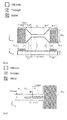
- the figure 9a shows an image obtained by electron microscopy (parts of the image, without interest for the understanding of the invention, are hidden).
- the figure 9b is a detail view showing the injectors I1, I2.
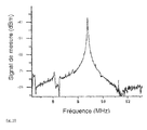
- the figure 10 illustrates the results of a measurement performed by exciting the oscillation of the system by injecting an electrical signal of amplitude 2dBm, the frequency of which sweeps the range 2 - 6.5 MHz.
- the mechanical oscillation of the system is detected by applying a DC bias voltage of 0.2 V to a detection circuit.
- the measurement curve, reproduced in the figure shows a lorentzian-type peak, with a resonant frequency at 8.78 MHz.
- the figure 7 shows a microelectromechanical system similar to that of the figure 6 but using two devices of the type of the figure 5 , allowing actuation and differential type detection.
- the references PLM2, PLS1, PLS2 110 designate the contact pads and the injectors of the first device D, the references PLM2 ', PLS1', PLS2 ', 110' the corresponding elements of the second device D '.
- Device D is used in operation; its pads PLS1, PLS2 are connected to a differential actuating circuit CAD to receive two alternating electric signals of the same frequency and in phase opposition, obtained by using a common generator and a phase shifter of 180 °, superimposed on a DC component.
- the device D ' is used in detection; its pads PLS1 ', PLS2' are connected to the inputs of a differential detection circuit CDD.
- the figure 8 illustrates a microelectromechanical accelerometer type system using two devices D, D 'of the type of the figure 3b .
- the references I1, I2, PLM1, PLM2, PLS1, PLS2 represent the injectors and the contact pads of the device D, the references I1 ', I2', PLM1 ', PLM2', PLS1 ', PLS2' the same elements of the device D .
- the system includes a PL beam member, extending in a y direction, connected to a moving mass MM via another PMM beam extending in the perpendicular direction x.
- This mobile mass is anchored in AMM1 and AMM2.
- One of the two devices, D for example makes it possible to put the PMM beam in oscillation while the second system, D 'for example, measures the resonance frequency of said beam.
- the moving mass moves, compresses or stretches the PMM beam and induces a detectable change in its resonant frequency.
Landscapes
- Physics & Mathematics (AREA)
- General Physics & Mathematics (AREA)
- Health & Medical Sciences (AREA)
- General Health & Medical Sciences (AREA)
- Nuclear Medicine, Radiotherapy & Molecular Imaging (AREA)
- Radiology & Medical Imaging (AREA)
- Engineering & Computer Science (AREA)
- Computer Hardware Design (AREA)
- Microelectronics & Electronic Packaging (AREA)
- Micromachines (AREA)
- Electrostatic, Electromagnetic, Magneto- Strictive, And Variable-Resistance Transducers (AREA)
Applications Claiming Priority (1)
| Application Number | Priority Date | Filing Date | Title |
|---|---|---|---|
| FR1560144A FR3042905B1 (fr) | 2015-10-23 | 2015-10-23 | Dispositif et systeme microelectromecanique avec transducteur resistif a faible impedance |
Publications (1)
| Publication Number | Publication Date |
|---|---|
| EP3159703A1 true EP3159703A1 (de) | 2017-04-26 |
Family
ID=55361630
Family Applications (1)
| Application Number | Title | Priority Date | Filing Date |
|---|---|---|---|
| EP16193853.5A Pending EP3159703A1 (de) | 2015-10-23 | 2016-10-14 | Mikroelektromechanische vorrichtung und system mit einem wandler mit einer schwachen impedanz |
Country Status (4)
| Country | Link |
|---|---|
| US (1) | US9815686B2 (de) |
| EP (1) | EP3159703A1 (de) |
| JP (1) | JP2017080872A (de) |
| FR (1) | FR3042905B1 (de) |
Families Citing this family (1)
| Publication number | Priority date | Publication date | Assignee | Title |
|---|---|---|---|---|
| FR3118830A1 (fr) | 2021-01-12 | 2022-07-15 | Commissariat A L'energie Atomique Et Aux Energies Alternatives | Dispositif de détection utilisant une transduction piézorésistive |
Citations (3)
| Publication number | Priority date | Publication date | Assignee | Title |
|---|---|---|---|---|
| EP1316977A2 (de) * | 2001-11-30 | 2003-06-04 | Nortel Networks Limited | Mikromechanischer Stellantrieb |
| WO2011038470A1 (en) * | 2009-09-29 | 2011-04-07 | Amg Technology Ltd. | Sensors for scanning probe microscopy, method for three-dimensional measurement and method for manufacturing such sensors |
| FR2964653A1 (fr) * | 2010-09-13 | 2012-03-16 | Commissariat Energie Atomique | Dispositif resonant a actionnement dans le plan, et procede de fabrication du dispositif |
Family Cites Families (5)
| Publication number | Priority date | Publication date | Assignee | Title |
|---|---|---|---|---|
| US6690178B2 (en) * | 2001-10-26 | 2004-02-10 | Rockwell Automation Technologies, Inc. | On-board microelectromechanical system (MEMS) sensing device for power semiconductors |
| WO2006060937A1 (en) * | 2004-12-10 | 2006-06-15 | Shanghai Institute Of Microsystem And Information Technology, Chinese Academy Of Sciences | A mems device including a laterally movable portion wiht piezo-resistive sensing elements and electrostatic actuating elements on trench side walls and methods for producing the same |
| US7966898B2 (en) * | 2006-07-28 | 2011-06-28 | California Institute Of Technology | Polymer NEMS for cell physiology and microfabricated cell positioning system for micro-biocalorimeter |
| PL2185910T3 (pl) * | 2007-08-20 | 2018-12-31 | Lifecare As | Urządzenie i sposób do mierzenia zwiększonego ciśnienia osmotycznego we wnęce odniesienia |
| KR101565988B1 (ko) * | 2009-10-23 | 2015-11-05 | 삼성전자주식회사 | 적색형광체, 그 제조방법, 이를 이용한 발광소자 패키지, 조명장치 |
-
2015
- 2015-10-23 FR FR1560144A patent/FR3042905B1/fr active Active
-
2016
- 2016-10-13 US US15/293,147 patent/US9815686B2/en active Active
- 2016-10-14 EP EP16193853.5A patent/EP3159703A1/de active Pending
- 2016-10-17 JP JP2016203283A patent/JP2017080872A/ja active Pending
Patent Citations (3)
| Publication number | Priority date | Publication date | Assignee | Title |
|---|---|---|---|---|
| EP1316977A2 (de) * | 2001-11-30 | 2003-06-04 | Nortel Networks Limited | Mikromechanischer Stellantrieb |
| WO2011038470A1 (en) * | 2009-09-29 | 2011-04-07 | Amg Technology Ltd. | Sensors for scanning probe microscopy, method for three-dimensional measurement and method for manufacturing such sensors |
| FR2964653A1 (fr) * | 2010-09-13 | 2012-03-16 | Commissariat Energie Atomique | Dispositif resonant a actionnement dans le plan, et procede de fabrication du dispositif |
Non-Patent Citations (3)
| Title |
|---|
| BEARDSLEE L A ET AL: "Thermal Excitation and Piezoresistive Detection of Cantilever In-Plane Resonance Modes for Sensing Applications", JOURNAL OF MICROELECTROMECHANICAL SYSTEMS, IEEE SERVICE CENTER, US, vol. 19, no. 4, 1 August 2010 (2010-08-01), pages 1015 - 1017, XP011312002, ISSN: 1057-7157 * |
| J. H. COMTOIS; V. M. BRIGHT; M. W. PHIPPS: "Thermal microactuators for surface-micromachining processes", PROC.SPIE 2642, MICROMACHINED DEVICES AND COMPONENTS, vol. 10, 15 September 1995 (1995-09-15) |
| L. A. BEARDSLEE; A. M. ADDOUS; S. HEINRICH; F. JOSSE; I. DUFOUR; O. BRAND: "Thermal Excitation and Piezoresistive Détection of Cantilever In-Plane Resonance Modes for Sensing Applications", JOURNAL OF MICROELECTROMECHANICAL SYSTEMS, vol. 19, no. 4, August 2010 (2010-08-01) |
Also Published As
| Publication number | Publication date |
|---|---|
| FR3042905A1 (fr) | 2017-04-28 |
| US20170113918A1 (en) | 2017-04-27 |
| JP2017080872A (ja) | 2017-05-18 |
| US9815686B2 (en) | 2017-11-14 |
| FR3042905B1 (fr) | 2018-11-16 |
Similar Documents
| Publication | Publication Date | Title |
|---|---|---|
| EP2796884B1 (de) | Mikroelektromechanische und/oder nanoelektromechanische Struktur mit einstellbarer Qualitätsfaktor | |
| EP2367015B1 (de) | Rauscharmer kraftsensor | |
| EP2711696B1 (de) | Wärmeflusssensor mit Schwingelement und Gas-Sensor mit wenigstens einem solchen Wärmeflusssensor | |
| EP2065713B1 (de) | Erfassungsvorrichtung mittels aufgehängtem Dehnungsmesser mit piezoelektrischem Widerstand, der eine Dehnungsverstärkungszelle umfasst | |
| EP2211185A1 (de) | Trägheitssensor oder Resonanzsensor in der Oberflächentechnologie zur Erkennung von Abweichungen mit Hilfe eines Dehnungsmessers | |
| WO2012038524A1 (fr) | Bolometre a detection frequentielle | |
| EP2592429B1 (de) | Vektorieller Magnetfeldsensor | |
| FR2964651A1 (fr) | Dispositif a poutre suspendue et moyens de detection piezoresistive du deplacement de celle-ci, et procede de fabrication du dispositif | |
| FR2986865A1 (fr) | Dispositif de detection compact d'au moins une acceleration et une vitesse de rotation | |
| CA2484591A1 (fr) | Accelerometre micro-usine multiaxes | |
| EP3159300A1 (de) | Mikroelektromechanische und/oder nanoelektromechanische struktur mit mindestens zwei unterschiedlich palarisierten thermischen aktuatoren | |
| EP3159703A1 (de) | Mikroelektromechanische vorrichtung und system mit einem wandler mit einer schwachen impedanz | |
| EP2890992B1 (de) | Vorrichtung zur messung von magnetfeldern mit laplace-kraft | |
| FR3012124A1 (fr) | Dispositif de detection electromecanique, pour la detection gravimetrique, et procede de fabrication du dispositif | |
| EP2715299B1 (de) | Dehnungssensor | |
| EP3312616B1 (de) | Miniaturisierte sonde für rasterkraftmikroskopie mit geringem platzbedarf | |
| EP1353185B1 (de) | Ineritalsensor mit integrierter Temperatursonde | |
| EP2862000B1 (de) | Sensor für magnetfelder mit laplace-kraft | |
| FR3118830A1 (fr) | Dispositif de détection utilisant une transduction piézorésistive | |
| EP3663752B1 (de) | Thermischer flusssensor mit heizbaren nanodrähten | |
| EP3558862B1 (de) | Mikroelektronische struktur mit kontrollierter viskoser dämpfung durch steuerung eines thermo-piezoresistiven effekts | |
| WO2014064273A1 (fr) | Reseau de connexion pour nems a agencement ameliore | |
| FR3014094A1 (fr) | Systeme mecanique micro-usine (nems) avec resistances d'adaptation | |
| EP4148432A1 (de) | Mikroelektromechanischer resonanzsensor mit entkopplungsmasse zwischen resonator und testmasse |
Legal Events
| Date | Code | Title | Description |
|---|---|---|---|
| PUAI | Public reference made under article 153(3) epc to a published international application that has entered the european phase |
Free format text: ORIGINAL CODE: 0009012 |
|
| STAA | Information on the status of an ep patent application or granted ep patent |
Free format text: STATUS: THE APPLICATION HAS BEEN PUBLISHED |
|
| AK | Designated contracting states |
Kind code of ref document: A1 Designated state(s): AL AT BE BG CH CY CZ DE DK EE ES FI FR GB GR HR HU IE IS IT LI LT LU LV MC MK MT NL NO PL PT RO RS SE SI SK SM TR |
|
| AX | Request for extension of the european patent |
Extension state: BA ME |
|
| STAA | Information on the status of an ep patent application or granted ep patent |
Free format text: STATUS: REQUEST FOR EXAMINATION WAS MADE |
|
| 17P | Request for examination filed |
Effective date: 20171018 |
|
| RBV | Designated contracting states (corrected) |
Designated state(s): AL AT BE BG CH CY CZ DE DK EE ES FI FR GB GR HR HU IE IS IT LI LT LU LV MC MK MT NL NO PL PT RO RS SE SI SK SM TR |
|
| STAA | Information on the status of an ep patent application or granted ep patent |
Free format text: STATUS: EXAMINATION IS IN PROGRESS |
|
| 17Q | First examination report despatched |
Effective date: 20190801 |
|
| STAA | Information on the status of an ep patent application or granted ep patent |
Free format text: STATUS: EXAMINATION IS IN PROGRESS |
|
| STAA | Information on the status of an ep patent application or granted ep patent |
Free format text: STATUS: EXAMINATION IS IN PROGRESS |