EP3158640B1 - A radio frequency oscillator - Google Patents
A radio frequency oscillator Download PDFInfo
- Publication number
- EP3158640B1 EP3158640B1 EP15701359.0A EP15701359A EP3158640B1 EP 3158640 B1 EP3158640 B1 EP 3158640B1 EP 15701359 A EP15701359 A EP 15701359A EP 3158640 B1 EP3158640 B1 EP 3158640B1
- Authority
- EP
- European Patent Office
- Prior art keywords
- oscillator
- circuit
- primary
- capacitor
- radio frequency
- Prior art date
- Legal status (The legal status is an assumption and is not a legal conclusion. Google has not performed a legal analysis and makes no representation as to the accuracy of the status listed.)
- Active
Links
Images





Classifications
-
- H—ELECTRICITY
- H03—ELECTRONIC CIRCUITRY
- H03B—GENERATION OF OSCILLATIONS, DIRECTLY OR BY FREQUENCY-CHANGING, BY CIRCUITS EMPLOYING ACTIVE ELEMENTS WHICH OPERATE IN A NON-SWITCHING MANNER; GENERATION OF NOISE BY SUCH CIRCUITS
- H03B5/00—Generation of oscillations using amplifier with regenerative feedback from output to input
- H03B5/08—Generation of oscillations using amplifier with regenerative feedback from output to input with frequency-determining element comprising lumped inductance and capacitance
- H03B5/12—Generation of oscillations using amplifier with regenerative feedback from output to input with frequency-determining element comprising lumped inductance and capacitance active element in amplifier being semiconductor device
- H03B5/1228—Generation of oscillations using amplifier with regenerative feedback from output to input with frequency-determining element comprising lumped inductance and capacitance active element in amplifier being semiconductor device the amplifier comprising one or more field effect transistors
-
- H—ELECTRICITY
- H03—ELECTRONIC CIRCUITRY
- H03B—GENERATION OF OSCILLATIONS, DIRECTLY OR BY FREQUENCY-CHANGING, BY CIRCUITS EMPLOYING ACTIVE ELEMENTS WHICH OPERATE IN A NON-SWITCHING MANNER; GENERATION OF NOISE BY SUCH CIRCUITS
- H03B5/00—Generation of oscillations using amplifier with regenerative feedback from output to input
- H03B5/08—Generation of oscillations using amplifier with regenerative feedback from output to input with frequency-determining element comprising lumped inductance and capacitance
- H03B5/12—Generation of oscillations using amplifier with regenerative feedback from output to input with frequency-determining element comprising lumped inductance and capacitance active element in amplifier being semiconductor device
- H03B5/1237—Generation of oscillations using amplifier with regenerative feedback from output to input with frequency-determining element comprising lumped inductance and capacitance active element in amplifier being semiconductor device comprising means for varying the frequency of the generator
- H03B5/124—Generation of oscillations using amplifier with regenerative feedback from output to input with frequency-determining element comprising lumped inductance and capacitance active element in amplifier being semiconductor device comprising means for varying the frequency of the generator the means comprising a voltage dependent capacitance
- H03B5/1243—Generation of oscillations using amplifier with regenerative feedback from output to input with frequency-determining element comprising lumped inductance and capacitance active element in amplifier being semiconductor device comprising means for varying the frequency of the generator the means comprising a voltage dependent capacitance the means comprising voltage variable capacitance diodes
-
- H—ELECTRICITY
- H03—ELECTRONIC CIRCUITRY
- H03B—GENERATION OF OSCILLATIONS, DIRECTLY OR BY FREQUENCY-CHANGING, BY CIRCUITS EMPLOYING ACTIVE ELEMENTS WHICH OPERATE IN A NON-SWITCHING MANNER; GENERATION OF NOISE BY SUCH CIRCUITS
- H03B5/00—Generation of oscillations using amplifier with regenerative feedback from output to input
- H03B5/08—Generation of oscillations using amplifier with regenerative feedback from output to input with frequency-determining element comprising lumped inductance and capacitance
- H03B5/12—Generation of oscillations using amplifier with regenerative feedback from output to input with frequency-determining element comprising lumped inductance and capacitance active element in amplifier being semiconductor device
- H03B5/1206—Generation of oscillations using amplifier with regenerative feedback from output to input with frequency-determining element comprising lumped inductance and capacitance active element in amplifier being semiconductor device using multiple transistors for amplification
- H03B5/1218—Generation of oscillations using amplifier with regenerative feedback from output to input with frequency-determining element comprising lumped inductance and capacitance active element in amplifier being semiconductor device using multiple transistors for amplification the generator being of the balanced type
-
- H—ELECTRICITY
- H03—ELECTRONIC CIRCUITRY
- H03B—GENERATION OF OSCILLATIONS, DIRECTLY OR BY FREQUENCY-CHANGING, BY CIRCUITS EMPLOYING ACTIVE ELEMENTS WHICH OPERATE IN A NON-SWITCHING MANNER; GENERATION OF NOISE BY SUCH CIRCUITS
- H03B5/00—Generation of oscillations using amplifier with regenerative feedback from output to input
- H03B5/08—Generation of oscillations using amplifier with regenerative feedback from output to input with frequency-determining element comprising lumped inductance and capacitance
- H03B5/12—Generation of oscillations using amplifier with regenerative feedback from output to input with frequency-determining element comprising lumped inductance and capacitance active element in amplifier being semiconductor device
- H03B5/1237—Generation of oscillations using amplifier with regenerative feedback from output to input with frequency-determining element comprising lumped inductance and capacitance active element in amplifier being semiconductor device comprising means for varying the frequency of the generator
- H03B5/1262—Generation of oscillations using amplifier with regenerative feedback from output to input with frequency-determining element comprising lumped inductance and capacitance active element in amplifier being semiconductor device comprising means for varying the frequency of the generator the means comprising switched elements
-
- H—ELECTRICITY
- H03—ELECTRONIC CIRCUITRY
- H03B—GENERATION OF OSCILLATIONS, DIRECTLY OR BY FREQUENCY-CHANGING, BY CIRCUITS EMPLOYING ACTIVE ELEMENTS WHICH OPERATE IN A NON-SWITCHING MANNER; GENERATION OF NOISE BY SUCH CIRCUITS
- H03B5/00—Generation of oscillations using amplifier with regenerative feedback from output to input
- H03B5/08—Generation of oscillations using amplifier with regenerative feedback from output to input with frequency-determining element comprising lumped inductance and capacitance
- H03B5/12—Generation of oscillations using amplifier with regenerative feedback from output to input with frequency-determining element comprising lumped inductance and capacitance active element in amplifier being semiconductor device
- H03B5/1237—Generation of oscillations using amplifier with regenerative feedback from output to input with frequency-determining element comprising lumped inductance and capacitance active element in amplifier being semiconductor device comprising means for varying the frequency of the generator
- H03B5/1262—Generation of oscillations using amplifier with regenerative feedback from output to input with frequency-determining element comprising lumped inductance and capacitance active element in amplifier being semiconductor device comprising means for varying the frequency of the generator the means comprising switched elements
- H03B5/1265—Generation of oscillations using amplifier with regenerative feedback from output to input with frequency-determining element comprising lumped inductance and capacitance active element in amplifier being semiconductor device comprising means for varying the frequency of the generator the means comprising switched elements switched capacitors
-
- H—ELECTRICITY
- H03—ELECTRONIC CIRCUITRY
- H03B—GENERATION OF OSCILLATIONS, DIRECTLY OR BY FREQUENCY-CHANGING, BY CIRCUITS EMPLOYING ACTIVE ELEMENTS WHICH OPERATE IN A NON-SWITCHING MANNER; GENERATION OF NOISE BY SUCH CIRCUITS
- H03B5/00—Generation of oscillations using amplifier with regenerative feedback from output to input
- H03B5/08—Generation of oscillations using amplifier with regenerative feedback from output to input with frequency-determining element comprising lumped inductance and capacitance
- H03B5/12—Generation of oscillations using amplifier with regenerative feedback from output to input with frequency-determining element comprising lumped inductance and capacitance active element in amplifier being semiconductor device
- H03B5/1237—Generation of oscillations using amplifier with regenerative feedback from output to input with frequency-determining element comprising lumped inductance and capacitance active element in amplifier being semiconductor device comprising means for varying the frequency of the generator
- H03B5/1293—Generation of oscillations using amplifier with regenerative feedback from output to input with frequency-determining element comprising lumped inductance and capacitance active element in amplifier being semiconductor device comprising means for varying the frequency of the generator having means for achieving a desired tuning characteristic, e.g. linearising the frequency characteristic across the tuning voltage range
-
- H—ELECTRICITY
- H03—ELECTRONIC CIRCUITRY
- H03B—GENERATION OF OSCILLATIONS, DIRECTLY OR BY FREQUENCY-CHANGING, BY CIRCUITS EMPLOYING ACTIVE ELEMENTS WHICH OPERATE IN A NON-SWITCHING MANNER; GENERATION OF NOISE BY SUCH CIRCUITS
- H03B5/00—Generation of oscillations using amplifier with regenerative feedback from output to input
- H03B5/08—Generation of oscillations using amplifier with regenerative feedback from output to input with frequency-determining element comprising lumped inductance and capacitance
- H03B5/12—Generation of oscillations using amplifier with regenerative feedback from output to input with frequency-determining element comprising lumped inductance and capacitance active element in amplifier being semiconductor device
- H03B5/1296—Generation of oscillations using amplifier with regenerative feedback from output to input with frequency-determining element comprising lumped inductance and capacitance active element in amplifier being semiconductor device the feedback circuit comprising a transformer
-
- H—ELECTRICITY
- H03—ELECTRONIC CIRCUITRY
- H03F—AMPLIFIERS
- H03F1/00—Details of amplifiers with only discharge tubes, only semiconductor devices or only unspecified devices as amplifying elements
- H03F1/56—Modifications of input or output impedances, not otherwise provided for
- H03F1/565—Modifications of input or output impedances, not otherwise provided for using inductive elements
-
- H—ELECTRICITY
- H03—ELECTRONIC CIRCUITRY
- H03F—AMPLIFIERS
- H03F3/00—Amplifiers with only discharge tubes or only semiconductor devices as amplifying elements
- H03F3/189—High-frequency amplifiers, e.g. radio frequency amplifiers
- H03F3/19—High-frequency amplifiers, e.g. radio frequency amplifiers with semiconductor devices only
- H03F3/193—High-frequency amplifiers, e.g. radio frequency amplifiers with semiconductor devices only with field-effect devices
-
- H—ELECTRICITY
- H03—ELECTRONIC CIRCUITRY
- H03F—AMPLIFIERS
- H03F3/00—Amplifiers with only discharge tubes or only semiconductor devices as amplifying elements
- H03F3/20—Power amplifiers, e.g. Class B amplifiers, Class C amplifiers
- H03F3/24—Power amplifiers, e.g. Class B amplifiers, Class C amplifiers of transmitter output stages
- H03F3/245—Power amplifiers, e.g. Class B amplifiers, Class C amplifiers of transmitter output stages with semiconductor devices only
-
- H—ELECTRICITY
- H03—ELECTRONIC CIRCUITRY
- H03F—AMPLIFIERS
- H03F3/00—Amplifiers with only discharge tubes or only semiconductor devices as amplifying elements
- H03F3/72—Gated amplifiers, i.e. amplifiers which are rendered operative or inoperative by means of a control signal
-
- H—ELECTRICITY
- H03—ELECTRONIC CIRCUITRY
- H03L—AUTOMATIC CONTROL, STARTING, SYNCHRONISATION OR STABILISATION OF GENERATORS OF ELECTRONIC OSCILLATIONS OR PULSES
- H03L7/00—Automatic control of frequency or phase; Synchronisation
-
- H—ELECTRICITY
- H04—ELECTRIC COMMUNICATION TECHNIQUE
- H04B—TRANSMISSION
- H04B1/00—Details of transmission systems, not covered by a single one of groups H04B3/00 - H04B13/00; Details of transmission systems not characterised by the medium used for transmission
- H04B1/38—Transceivers, i.e. devices in which transmitter and receiver form a structural unit and in which at least one part is used for functions of transmitting and receiving
- H04B1/40—Circuits
- H04B1/44—Transmit/receive switching
-
- H—ELECTRICITY
- H03—ELECTRONIC CIRCUITRY
- H03B—GENERATION OF OSCILLATIONS, DIRECTLY OR BY FREQUENCY-CHANGING, BY CIRCUITS EMPLOYING ACTIVE ELEMENTS WHICH OPERATE IN A NON-SWITCHING MANNER; GENERATION OF NOISE BY SUCH CIRCUITS
- H03B2201/00—Aspects of oscillators relating to varying the frequency of the oscillations
- H03B2201/02—Varying the frequency of the oscillations by electronic means
- H03B2201/025—Varying the frequency of the oscillations by electronic means the means being an electronic switch for switching in or out oscillator elements
- H03B2201/0266—Varying the frequency of the oscillations by electronic means the means being an electronic switch for switching in or out oscillator elements the means comprising a transistor
Definitions
- the invention relates to the field of radio frequency (RF) oscillators.
- Radio frequency oscillators are widely used in a variety of applications, such as for instance multi-mode multi-band applications.
- Radio frequency oscillators usually comprise resonator circuits as frequency selective elements, wherein the resonator circuits comprise inductors and capacitors.
- the inductors and capacitors are connected to be in resonance at a specific resonance frequency.
- different approaches are applied for providing a high tuning range of a radio frequency oscillator.
- An exemplary approach to provide an increased tuning range is to employ two separate radio frequency oscillators having separate resonator circuits and using high frequency multiplexers, which can lead to an increased power consumption and noise floor and can demand for a large die area.
- L. Fanori et al. "A 2.4-to-5.3 GHz dual core CMOS VCO with concentric 8-shape coils," ISSCC Dig. Tech. Papers, pp 370-372, 17-21 Feb. 2013 , a topology having separate resonator circuits is described.
- a further exemplary approach is based on switching between even and odd resonance modes of a high-order LC resonator circuit within a radio frequency oscillator.
- a separation of resonance peaks in the different modes can be achieved, however, leading to a large size of the LC resonator circuit.
- G. Li. et al. A Distributed dual-band LC oscillator based on Mode Switching," IEEE TMTT, vol. 59, no. 1, pp. 99-107, Jan 2011 , a topology using mode switching is described.
- Radio frequency oscillators providing a high tuning range suffer from an increased noise floor and/or an increased size, in particular when implemented as radio frequency integrated circuits (RFICs) on semiconductor substrates.
- RFICs radio frequency integrated circuits
- US 2012/0161890 A1 describes a VCO including an LC resonator having an even and odd resonant mode.
- US 2011/0018644 A1 relates to an oscillator connected to a resonance unit suited to oscillate frequencies in multiple bands.
- DONGHYUN BAEK ET AL "A dual-band (13/22-GHz) VCO based on resonant mode switching", IEEE MICROWAVE AND WIRELESS COMPONENTS LETTERS, IEEE SERVICE CENTER, NEW YORK, NY, US, vol. 13, no. 10, 1 October 2003 (2003-10-01), pages 443-445, XP011427858 , relates to a dual band voltage controlled oscillator that can cover two bands.
- US 6606008 B2 discloses that high voltage swing can be achieved at the input of the transistors, and can be increased further through a suitable choice of turns ratios of the transformers, enabling the use of comparatively small transistor structures for the transistors, which can be operated with a high current density.
- a primary inductor and/or a secondary inductor may have any suitable number of turns.
- the primary inductor and secondary inductor may have the same number of turns.
- the primary inductor may have more turns or less turns than the secondary inductor.
- the invention is based on the finding that a resonator circuit can be employed, wherein the resonator circuit is resonant at an excitation in a differential mode and at an excitation in a common mode.
- the resonator circuit can have different resonance frequencies when excited in the differential mode and the common mode, wherein the differential mode resonance frequency and the common mode resonance frequency can be tunable. This difference may be due to a different magnetic or inductive coupling factor, km, when the resonator circuit is excited in the differential mode or the common mode.
- the coupling factor may be high, while in the common mode the coupling factor may be low.
- the resonator circuit is excited by a first excitation circuit in the differential mode and by a second excitation circuit in the common mode. Therefore, a differential mode oscillator signal oscillating at the differential mode resonance frequency and a common mode oscillator signal oscillating at the common mode resonance frequency are provided.
- the resonator circuit and the first excitation circuit are arranged to form a cross-coupled oscillator or a transformer-coupled oscillator.
- the resonator circuit and the second excitation circuit are arranged to form a Colpitts oscillator. Consequently, the radio frequency oscillator employs a single resonator circuit or tank circuit. Furthermore, extra tuning range can be gained using the common mode oscillation without any area penalty or degradation of the differential mode oscillation performance.
- the radio frequency oscillator and the resonator circuit can be compact.
- the resonator circuit and the radio frequency oscillator are suited for implementation as radio frequency integrated circuits (RFICs) on semiconductor substrates.
- the invention relates to a radio frequency oscillator, the radio frequency oscillator comprising a resonator circuit being resonant at an excitation of the resonator circuit in a differential mode and at an excitation of the resonator circuit in a common mode, wherein the resonator circuit has a differential mode resonance frequency at the excitation in the differential mode, and wherein the resonator circuit has a common mode resonance frequency at the excitation in the common mode and comprises a transformer (201), a primary capacitor (207), and a secondary capacitor (209), wherein the transformer (201) comprises a primary winding (203) and a secondary winding (205), the primary winding (203) being inductively coupled with the secondary winding (205), wherein the primary capacitor (207) is connected to the primary winding (203), the primary capacitor (207) and the primary winding (203) forming a primary circuit, and wherein the secondary capacitor (209) is connected to the secondary winding (205), the secondary capacitor (209) and the secondary winding (205) forming
- the radio frequency oscillator further comprises a first excitation circuit being configured to excite the resonator circuit in the differential mode to obtain a differential mode oscillator signal oscillating at the differential mode resonance frequency, and a second excitation circuit being configured to excite the resonator circuit in the common mode to obtain a common mode oscillator signal oscillating at the common mode resonance frequency, wherein a ratio of turns of the primary and secondary windings is 1:2.
- the resonator circuit (101) and the first excitation circuit (103) are arranged to form a cross-coupled oscillator or a transformer-coupled oscillator to obtain the differential mode oscillator signal.
- the resonator circuit (101) and the second excitation circuit (105) are arranged to form a Colpitts oscillator to obtain the common mode oscillator signal.
- an efficient radio frequency oscillator is provided and an efficient resonator circuit is used within the radio frequency oscillator.
- the radio frequency oscillator can be a dual-mode radio frequency oscillator providing the differential mode oscillator signal and the common mode oscillator signal.
- the resonator circuit can be a tank circuit.
- the resonator circuit can be used as a frequency selective element within the radio frequency oscillator.
- the resonator circuit is resonant when exited in the differential mode and in the common mode.
- the differential mode resonance frequency can depend on the inductance of the primary winding, the inductance of the secondary winding, the capacitance of the primary capacitor, and the capacitance of the secondary capacitor.
- the common mode resonance frequency can depend on the inductance of the primary winding and the capacitance of the primary capacitor.
- the common mode resonance frequency may not depend on the inductance of the secondary winding and the capacitance of the secondary capacitor.
- the resonator circuit has the common mode resonance frequency at an excitation of the primary circuit in the common mode, and the resonator circuit has the differential mode resonance frequency at an excitation of the primary circuit in the differential mode.
- the differential mode oscillator signal and the common mode oscillator signal can be provided efficiently.
- the primary winding and the secondary winding can be arranged to provide a strong inductive coupling when the primary circuit is excited in the differential mode and a weak inductive coupling when the primary circuit is excited in the common mode.
- the primary winding of the transformer comprises one turn
- the secondary winding of the transformer comprises two turns.
- induced currents at the secondary winding can have the same direction resulting in a strong coupling factor.
- a common mode excitation of the primary winding can induce currents at the secondary winding that circulate in opposite directions canceling each other resulting in a weak coupling factor.
- a 2:1 transformer can have the same properties and can be used alternatively. 1:2 transformers and 2:1 transformers can be smallest size transformers having this property thus being area efficient.
- the primary capacitor can comprise a pair of single-ended capacitors for an efficient provision of a common mode oscillation.
- the primary winding of the transformer and/or the secondary winding of the transformer is planar.
- a resonator circuit with area efficiency is provided.
- the primary winding of the transformer and the secondary winding of the transformer are arranged on the same plane.
- a high coupling factor in differential mode and a low coupling factor in common mode is provided efficiently.
- the coupling factor in differential mode may be not as high as for the primary winding and the secondary winding of the transformer being arranged on the same plane.
- the winding being arranged at a lower metal plane can have a reduced quality factor Q and can yield a decreased phase noise performance.
- a high coupling factor in differential mode and a low coupling factor in common mode is thus provided efficiently.
- the primary winding of the transformer and/or the secondary winding of the transformer can comprise a bridging portion being arranged at a different plane.
- the primary winding of the transformer and/or the secondary winding of the transformer is connected to a constant voltage source or a ground potential.
- a tapping of the primary winding and/or the secondary winding is realized.
- Both the primary winding and the secondary winding may be connected to a constant voltage source respectively in order to enable an efficient start-up of the radio frequency oscillator.
- the tapping of the primary winding and/or the secondary winding can be a symmetrical center tapping of the primary winding and/or the secondary winding.
- the center tapping at the primary winding can reduce the common mode resonance frequency and can increase an overlap between differential mode and common mode oscillation frequencies. This may not influence the tuning range of the radio frequency oscillator.
- the primary capacitor of the primary circuit comprises a pair of single-ended capacitors.
- a reference to ground potential of the primary circuit is realized.
- the secondary capacitor of the secondary circuit comprises a pair of differential capacitors.
- the pair of differential capacitors can be a pair of balanced capacitors.
- the primary capacitor and/or the secondary capacitor comprises a variable capacitor, in particular a digitally tunable capacitor.
- the primary capacitor is connected in parallel to the primary winding, and/or the secondary capacitor is connected in parallel to the secondary winding.
- the primary circuit and the secondary circuit are realized as parallel circuits.
- the first excitation circuit and/or the second excitation circuit comprises at least one transistor, in particular at least one field-effect transistor, for exciting the resonator circuit.
- an active device is employed for exciting the resonator circuit.
- the transistor can be a trans-conductance gm transistor. In order to realize a cross-coupled structure at least two transistors may be employed.
- the transistors can be metal-oxide-semiconductor field-effect transistors (MOSFETs).
- the Colpitts oscillator comprises a first auxiliary oscillator and a second auxiliary oscillator, the first auxiliary oscillator being synchronizable with regard to the second auxiliary oscillator in frequency and phase.
- the two auxiliary oscillators comprised by the Colpitts oscillator can be locked together via a switch realized by a transistor, e.g. a MOS transistor. This switch can be off and can disconnect the outputs of the two auxiliary oscillators when the oscillator works in differential mode excitation.
- a differential mode oscillation can e.g. be provided when the Colpitts oscillator is off and the transformer-coupled oscillator is on.
- the Colpitts oscillator is a single-ended oscillator.
- a reference to ground otential is realized.
- the invention can be implemented using hardware and/or software.
- radio frequency oscillators for multi-mode multi-band cellular applications can demand for a high tuning range (TR) while ensuring low phase noise (PN) for a wide range of frequency bands and channels.
- TR tuning range
- PN phase noise
- Low quality factors Q of resonator circuits e.g. comprising switched-capacitor networks for wide tuning ranges, can limit the phase noise performance of radio frequency oscillators.
- Embodiments of the invention are based on an increased tuning range of a radio frequency oscillator having a single resonator circuit by introducing a common mode oscillation.
- the common mode oscillation increases the tuning range of the radio frequency oscillator without any die area and/or phase noise penalty.
- the radio frequency oscillator can be regarded as a dual-mode radio frequency oscillator having a single resonator circuit.
- the resonator circuit can also be referred to as a tank circuit.
- Fig. 1 shows a diagram of a radio frequency oscillator 100 depicting some of the features of the claimed invention.
- the radio frequency oscillator 100 comprises a resonator circuit 101 being resonant at an excitation of the resonator circuit 101 in a differential mode and at an excitation of the resonator circuit 101 in a common mode, wherein the resonator circuit 101 has a differential mode resonance frequency at the excitation in the differential mode, and wherein the resonator circuit 101 has a common mode resonance frequency at the excitation in the common mode, a first excitation circuit 103 being configured to excite the resonator circuit 101 in the differential mode to obtain a differential mode oscillator signal oscillating at the differential mode resonance frequency, and a second excitation circuit 105 being configured to excite the resonator circuit 101 in the common mode to obtain a common mode oscillator signal oscillating at the common mode resonance frequency.
- the resonator circuit 101 comprises a transformer, a primary capacitor, and a secondary capacitor, wherein the transformer comprises a primary winding and a secondary winding, the primary winding being inductively coupled with the secondary winding, wherein the primary capacitor is connected to the primary winding, the primary capacitor and the primary winding forming a primary circuit, and wherein the secondary capacitor is connected to the secondary winding, the secondary capacitor and the secondary winding forming a secondary circuit.
- Fig. 2 shows a diagram of a resonator circuit 101 depicting some of the features of the claimed invention.
- the resonator circuit 101 is resonant at an excitation of the resonator circuit 101 in a differential mode and at an excitation of the resonator circuit 101 in a common mode, wherein the resonator circuit 101 has a differential mode resonance frequency at the excitation in the differential mode, and wherein the resonator circuit 101 has a common mode resonance frequency at the excitation in the common mode.
- the resonator circuit 101 comprises a transformer 201, a primary capacitor 207, and a secondary capacitor 209, wherein the transformer 201 comprises a primary winding 203 and a secondary winding 205, the primary winding 203 being inductively coupled with the secondary winding 205, wherein the primary capacitor 207 is connected to the primary winding 203, the primary capacitor 207 and the primary winding 203 forming a primary circuit, and wherein the secondary capacitor 209 is connected to the secondary winding 205, the secondary capacitor 209 and the secondary winding 205 forming a secondary circuit.
- the resonator circuit 101 has the common mode resonance frequency at an excitation of the primary circuit in the common mode.
- the resonator circuit 101 has the differential mode resonance frequency at an excitation of the primary circuit in the differential mode.
- Fig. 3 shows a diagram of a resonator circuit 101 depicting some of the features of the claimed invention.
- the resonator circuit 101 comprises a transformer 201, a primary capacitor 207, and a secondary capacitor 209, wherein the transformer 201 comprises a primary winding 203 and a secondary winding 205, the primary winding 203 being inductively coupled with the secondary winding 205, wherein the primary capacitor 207 is connected to the primary winding 203, the primary capacitor 207 and the primary winding 203 forming a primary circuit, and wherein the secondary capacitor 209 is connected to the secondary winding 205, the secondary capacitor 209 and the secondary winding 205 forming a secondary circuit.
- the primary capacitor 207 of the primary circuit comprises a pair of single-ended capacitors 301, 303.
- the secondary capacitor 209 of the secondary circuit comprises a pair of differential capacitors 305, 307.
- k m denotes the magnetic or inductive coupling factor between the primary winding 203 and the secondary winding 205, wherein 0 ⁇
- the inductance of the primary winding 203 can be referred to as L p
- the inductance of the secondary winding 205 can be referred to as L s
- the capacitance of the primary capacitor 207 can be referred to as C p
- the capacitance of the secondary capacitor 209 can be referred to as C s .
- the primary winding 203, the secondary winding 205, the primary capacitor 207, and the secondary capacitor 209 are considered as individual concentrated components.
- the inductance of the primary winding 203 can be referred to as 2 L p
- the inductance of the secondary winding 205 can be referred to as 2 L s
- the capacitance of the primary capacitor 207 can be referred to as 0.5 C p
- the capacitance of the secondary capacitor 209 can be referred to as 0.5 C s
- the primary winding 203 and the secondary winding 205 are each formed by a pair of inductors connected in series, wherein the inductance of each inductor is referred to as L p or L s , respectively.
- the primary capacitor 207 and the secondary capacitor 209 are each formed by a pair of capacitors connected in series, wherein the capacitance of each capacitor is referred to as C p or C s , respectively.
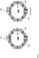
- Fig. 4 shows a diagram of a transformer 201 of a resonator circuit 101 depicting some of the features of the claimed invention.
- the transformer 201 comprises a primary winding 203 and a secondary winding 205, the primary winding 203 being inductively coupled with the secondary winding 205.
- the primary winding 203 comprises one turn and the secondary winding 205 comprises two turns, realizing a ratio of turns of 1:2.
- the diagram illustrates induced currents within the transformer 201 at an excitation in differential mode (DM) and an excitation in common mode (CM).
- DM differential mode
- CM excitation in common mode
- Embodiments of the invention are based on different resonance frequencies of the transformer-based resonator circuit 101 at differential mode excitations and common mode excitations.
- the different resonance frequencies can be due to a different inductive coupling factor k m when the primary winding 203 of the transformer 201 is excited by differential mode or common mode signals.
- the induced currents at the secondary winding 205 at differential mode excitation can circulate in same directions and can provide a high coupling factor k m between the primary winding 203 and the secondary winding 205 of the transformer 201. Consequently, in differential mode, the inductance of the secondary winding 205 and the capacitance of the secondary capacitor 209 can strongly affect the differential mode characteristics of the resonator circuit 101, e.g. the differential mode resonance frequency.
- the induced currents at the secondary winding 205 at common mode excitation can circulate in opposite directions and can cancel each other.
- the coupling factor k m can be low in the common mode, e.g. k m,CM ⁇ 0.3. This low coupling factor k m can be interpreted as the secondary winding 205 not being seen from the primary winding 203.
- the common mode resonance frequency ⁇ 0,CM can be higher than the differential mode resonance frequency ⁇ 0,DM and the frequency separation can be controlled by the ratio L s C s /L p C p .
- the inductance associated with the primary winding 203 in common mode L pc can be different from the inductance associated with the primary winding 203 in differential mode L pd . It can be considered in the design phase that L pc >L pd .
- Fig. 5 shows a diagram of an input impedance response 501 of a resonator circuit 101 according to an embodiment.
- the diagram illustrates differential mode resonance frequencies and common mode resonance frequencies.
- the input impedance of the resonator circuit 101 is denoted as Z in .
- the quality factor in common mode Qc can be slightly less than the quality factor in differential mode Q D but may be large enough such that oscillation is possible in this mode. If the quality factor of a resonator circuit is large, an oscillation start-up can easier be realized. In the diagram, Qc is smaller than Q D but is still large enough for an efficient oscillation start-up.
- both the differential mode resonance frequency and the common mode resonance frequency can vary, e.g. by 34%.
- the resonance frequencies can cover an octave while going from differential mode oscillations to common mode oscillations.
- the ratio C max /C min may be greater than 2, due to parasitic effects and challenges associated with controlling the precise overlap between the differential mode resonance frequencies and the common mode resonance frequencies.
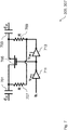
- Fig. 6 shows a diagram of a single-ended capacitor 301, 303 according to an embodiment.
- the single-ended capacitor 301, 303 comprises a capacitor 601, a capacitor 603, a transistor 605, a transistor 607, a resistor 609, a resistor 611, an inverter 613, and an inverter 615.
- the single-ended capacitor 301, 303 is arranged within the primary circuit of the resonator circuit 101.
- the transistor 605 and the transistor 607 can be switched between a conducting state and a non-conducting state. Consequently, the capacitance of the single-ended capacitor 301, 303 can be digitally tuned.
- a plurality of single-ended capacitors 301, 303 can be connected in parallel.
- Fig. 7 shows a diagram of a differential capacitor 305, 307 according to an embodiment.
- the differential capacitor 305, 307 comprises a capacitor 701, a capacitor 703, a transistor 705, a resistor 707, a resistor 709, an inverter 711, and an inverter 713.
- the differential capacitor 305, 307 is arranged within the secondary circuit of the resonator circuit 101.
- the transistor 705 By applying a digital switching signal bi, the transistor 705 can be switched between a conducting state and a non-conducting state. Consequently, the capacitance of the differential capacitor 305, 307 can be digitally tuned.
- a plurality of differential capacitors 305, 307 can be connected in parallel.
- Fig. 8 shows a diagram of an input inductance response 801 and a coupling factor response 803 according to an embodiment.
- the input inductance 801 relates to the inductances of the primary winding 203 and the secondary winding 205 of the transformer 201.
- the inductance 2 L s is approximately 1.5 nH.
- the inductance 2 L pd is approximately 0.5 nH.
- the inductance L pc is approximately 0.4 nH. The inductances slightly increase with frequency.
- the coupling factor response 803 relates to coupling factors of the transformer 201 at an excitation in differential mode and in common mode.
- the coupling factor in differential mode k md is approximately 0.7.
- the coupling factor in common mode k mc is approximately 0.25.
- the coupling factors slightly increase with frequency.
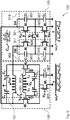
- Fig. 9 shows a diagram of a radio frequency oscillator 100 according to an embodiment of the claimed invention.
- the radio frequency oscillator 100 comprises a resonator circuit 101 being resonant at an excitation of the resonator circuit 101 in a differential mode and at an excitation of the resonator circuit 101 in a common mode, wherein the resonator circuit 101 has a differential mode resonance frequency at the excitation in the differential mode, and wherein the resonator circuit 101 has a common mode resonance frequency at the excitation in the common mode, a first excitation circuit 103 being configured to excite the resonator circuit 101 in the differential mode to obtain a differential mode oscillator signal oscillating at the differential mode resonance frequency, and a second excitation circuit 105 being configured to excite the resonator circuit 101 in the common mode to obtain a common mode oscillator signal oscillating at the common mode resonance frequency.
- the resonator circuit 101 forms an implementation of the resonator circuit 101 as described in conjunction with Fig. 3 .
- the first excitation circuit 103 comprises a transistor 901, a transistor 903, a tail transistor 905, and a tail capacitor 907.
- the second excitation circuit 105 comprises a first auxiliary oscillator 909, the first auxiliary oscillator 909 comprising a transistor 911, a capacitor 913, a transistor 915, and a capacitor 917.
- the second excitation circuit 105 further comprises a second auxiliary oscillator 919, the second auxiliary oscillator 919 comprising a transistor 921, a capacitor 923, a transistor 925, and a capacitor 927.
- the resonator circuit 101 and the first excitation circuit 103 are arranged to form a transformer-coupled oscillator to obtain the differential mode oscillator signal.
- the resonator circuit 101 and the second excitation circuit 105 are arranged to form a Colpitts oscillator to obtain the common mode oscillator signal.
- the first auxiliary oscillator 909 and the second auxiliary oscillator 919 are connected by a transistor 929.
- the first auxiliary oscillator 909 is synchronizable with regard to the second auxiliary oscillator 919 in frequency and phase via the transistor 929.
- the first auxiliary oscillator 909 can be injection-locked on the second auxiliary oscillator 919.
- Exciting the resonator circuit 101, in particular the transformer 201 of Fig. 2 , in the differential mode to obtain the differential mode oscillator signal oscillating at the differential mode resonance frequency can be achieved e.g. by using a cross-coupled gm-pair structure or a transformer-coupled structure within the first excitation circuit 103.
- a separate second excitation circuit 105 may be used in order to excite the resonator circuit 101 in the common mode.
- a dual mode oscillation in terms of a differential mode oscillation and a common mode oscillation can be provided.
- the described structure is depicted in Fig. 9 .
- the first excitation circuit 103 of the radio frequency oscillator 100 is structured according to a transformer-coupled structure for obtaining the differential mode oscillation in conjunction with the resonator circuit 101.
- the second excitation circuit 105 of the radio frequency oscillator 100 is structured as a Colpitts oscillator in conjunction with the resonator circuit 101.
- the Colpitts oscillator is single-ended.
- the Colpitts oscillator comprises two auxiliary oscillators 909, 919, in particular two cores, with the auxiliary oscillators 909, 919 being injection-locked through the transistor 929 or M7 switch. Both auxiliary oscillators 909, 919 can start oscillating at the same frequency but slightly out of phase.
- the auxiliary oscillators 909, 919 can lock and there may be no phase shift between them. Therefore, the resonator circuit 101, in particular the transformer, is excited in the common mode to obtain the common mode oscillator signal oscillating at the common mode resonance frequency.
- the injection-locking of the two auxiliary oscillators 909, 919 can lead to a 3dB improvement in phase noise performance.
- the radio frequency oscillator 100 can exhibit a phase noise characteristic having two distinctive regions.
- C eq can be designed to be larger than C p through the tuning range. This may reduce the tuning range of both the differential mode and common mode oscillations. The reduced tuning range can be more visible in common mode since in differential mode the primary and secondary capacitors can both affect the resonance frequency. By choosing L s C s > L p C p , this effect can be reduced even more in differential mode, without changing the common mode conditions.
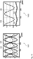
- Fig. 10 shows a diagram of differential mode oscillator signals 1001 and common mode oscillator signals 1003 according to an embodiment.
- the differential mode oscillator signals 1001 and the common mode oscillator signals 1003 are depicted for probe positions GA, GB, DA, and DB as shown in Fig. 9 .
- the differential mode oscillator signals 1001 and the common mode oscillator signals 1003 are sinusoidal signals over time.
- Embodiments of the invention use different characteristics of a 1:2 transformer 201 in differential mode excitation and in common mode excitation, and use an additional common mode oscillator signal to a differential mode oscillator signal, using the same resonator circuit 101 and hence imply no die area penalty. Furthermore, since differential mode and common mode start-up circuits can share the same output, there may be no need for multiplexing and hence no noise floor degradation.
Landscapes
- Engineering & Computer Science (AREA)
- Power Engineering (AREA)
- Computer Networks & Wireless Communication (AREA)
- Signal Processing (AREA)
- Inductance-Capacitance Distribution Constants And Capacitance-Resistance Oscillators (AREA)
Description
- The invention relates to the field of radio frequency (RF) oscillators.
- Radio frequency oscillators are widely used in a variety of applications, such as for instance multi-mode multi-band applications. Radio frequency oscillators usually comprise resonator circuits as frequency selective elements, wherein the resonator circuits comprise inductors and capacitors. The inductors and capacitors are connected to be in resonance at a specific resonance frequency. For providing a high tuning range of a radio frequency oscillator, different approaches are applied.
- An exemplary approach to provide an increased tuning range is to employ two separate radio frequency oscillators having separate resonator circuits and using high frequency multiplexers, which can lead to an increased power consumption and noise floor and can demand for a large die area. In L. Fanori et al., "A 2.4-to-5.3 GHz dual core CMOS VCO with concentric 8-shape coils," ISSCC Dig. Tech. Papers, pp 370-372, 17-21 Feb. 2013, a topology having separate resonator circuits is described.
- A further exemplary approach is based on switching between even and odd resonance modes of a high-order LC resonator circuit within a radio frequency oscillator. A separation of resonance peaks in the different modes can be achieved, however, leading to a large size of the LC resonator circuit. In G. Li. et al., A Distributed dual-band LC oscillator based on Mode Switching," IEEE TMTT, vol. 59, no. 1, pp. 99-107, Jan 2011, a topology using mode switching is described.
- Common radio frequency oscillators providing a high tuning range suffer from an increased noise floor and/or an increased size, in particular when implemented as radio frequency integrated circuits (RFICs) on semiconductor substrates.
-
US 2012/0161890 A1 describes a VCO including an LC resonator having an even and odd resonant mode. - The document "Transformer-Based Dual-Mode Voltage-Controlled Oscillators", IEEE TRANSACTIONS ON CIRCUITS AND SYSTEMS II: ANALOG AND DIGITALSIGNAL PROCESSING, INSTITUTE OF ELECTRICAL AND ELECTRONICS ENGINEERS INC, 345 EAST 47 STREET, NEW YORK, N.Y. 10017, USA, vol. 54, no. 4, 1 April 2007 (2007-04-01), pages 293-297, XP011176988 describes a dual-mode oscillator built using a transformer-based resonator.
-
US 2011/0018644 A1 relates to an oscillator connected to a resonance unit suited to oscillate frequencies in multiple bands. - DONGHYUN BAEK ET AL: "A dual-band (13/22-GHz) VCO based on resonant mode switching", IEEE MICROWAVE AND WIRELESS COMPONENTS LETTERS, IEEE SERVICE CENTER, NEW YORK, NY, US, vol. 13, no. 10, 1 October 2003 (2003-10-01), pages 443-445, XP011427858, relates to a dual band voltage controlled oscillator that can cover two bands.
-
US 6606008 B2 discloses that high voltage swing can be achieved at the input of the transistors, and can be increased further through a suitable choice of turns ratios of the transformers, enabling the use of comparatively small transistor structures for the transistors, which can be operated with a high current density. -
US 2013/0309983 A1 discloses that a primary inductor and/or a secondary inductor may have any suitable number of turns. The primary inductor and secondary inductor may have the same number of turns. The primary inductor may have more turns or less turns than the secondary inductor. - The present invention is as defined in the appended independent claim.
- It is an object of the invention to provide an efficient radio frequency oscillator.
- This object is achieved by the features of the independent claims. Further implementation forms are apparent from the dependent claims, the description and the figures.
- The invention is based on the finding that a resonator circuit can be employed, wherein the resonator circuit is resonant at an excitation in a differential mode and at an excitation in a common mode. The resonator circuit can have different resonance frequencies when excited in the differential mode and the common mode, wherein the differential mode resonance frequency and the common mode resonance frequency can be tunable. This difference may be due to a different magnetic or inductive coupling factor, km, when the resonator circuit is excited in the differential mode or the common mode. In particular, in the differential mode the coupling factor may be high, while in the common mode the coupling factor may be low.
- The resonator circuit is excited by a first excitation circuit in the differential mode and by a second excitation circuit in the common mode. Therefore, a differential mode oscillator signal oscillating at the differential mode resonance frequency and a common mode oscillator signal oscillating at the common mode resonance frequency are provided. The resonator circuit and the first excitation circuit are arranged to form a cross-coupled oscillator or a transformer-coupled oscillator. The resonator circuit and the second excitation circuit are arranged to form a Colpitts oscillator. Consequently, the radio frequency oscillator employs a single resonator circuit or tank circuit. Furthermore, extra tuning range can be gained using the common mode oscillation without any area penalty or degradation of the differential mode oscillation performance.
- Efficient structures of the radio frequency oscillator and the resonator circuit are provided, allowing for a high tuning range of the radio frequency oscillator while having a low size. The radio frequency oscillator and the resonator circuit can be compact. The resonator circuit and the radio frequency oscillator are suited for implementation as radio frequency integrated circuits (RFICs) on semiconductor substrates.
- According to a first aspect, the invention relates to a radio frequency oscillator, the radio frequency oscillator comprising a resonator circuit being resonant at an excitation of the resonator circuit in a differential mode and at an excitation of the resonator circuit in a common mode, wherein the resonator circuit has a differential mode resonance frequency at the excitation in the differential mode, and wherein the resonator circuit has a common mode resonance frequency at the excitation in the common mode and comprises a transformer (201), a primary capacitor (207), and a secondary capacitor (209), wherein the transformer (201) comprises a primary winding (203) and a secondary winding (205), the primary winding (203) being inductively coupled with the secondary winding (205), wherein the primary capacitor (207) is connected to the primary winding (203), the primary capacitor (207) and the primary winding (203) forming a primary circuit, and wherein the secondary capacitor (209) is connected to the secondary winding (205), the secondary capacitor (209) and the secondary winding (205) forming a secondary circuit. The radio frequency oscillator further comprises a first excitation circuit being configured to excite the resonator circuit in the differential mode to obtain a differential mode oscillator signal oscillating at the differential mode resonance frequency, and a second excitation circuit being configured to excite the resonator circuit in the common mode to obtain a common mode oscillator signal oscillating at the common mode resonance frequency, wherein a ratio of turns of the primary and secondary windings is 1:2. The resonator circuit (101) and the first excitation circuit (103) are arranged to form a cross-coupled oscillator or a transformer-coupled oscillator to obtain the differential mode oscillator signal. The resonator circuit (101) and the second excitation circuit (105) are arranged to form a Colpitts oscillator to obtain the common mode oscillator signal. Thus, an efficient radio frequency oscillator is provided and an efficient resonator circuit is used within the radio frequency oscillator.
- The radio frequency oscillator can be a dual-mode radio frequency oscillator providing the differential mode oscillator signal and the common mode oscillator signal.
- The resonator circuit can be a tank circuit. The resonator circuit can be used as a frequency selective element within the radio frequency oscillator. The resonator circuit is resonant when exited in the differential mode and in the common mode.
- The differential mode resonance frequency can depend on the inductance of the primary winding, the inductance of the secondary winding, the capacitance of the primary capacitor, and the capacitance of the secondary capacitor.
- The common mode resonance frequency can depend on the inductance of the primary winding and the capacitance of the primary capacitor. The common mode resonance frequency may not depend on the inductance of the secondary winding and the capacitance of the secondary capacitor.
- In a first implementation form of the radio frequency oscillator according to the first aspect, the resonator circuit has the common mode resonance frequency at an excitation of the primary circuit in the common mode, and the resonator circuit has the differential mode resonance frequency at an excitation of the primary circuit in the differential mode. Thus, the differential mode oscillator signal and the common mode oscillator signal can be provided efficiently.
- The primary winding and the secondary winding can be arranged to provide a strong inductive coupling when the primary circuit is excited in the differential mode and a weak inductive coupling when the primary circuit is excited in the common mode.
- In a second implementation form of the radio frequency oscillator according to the first implementation form or according to the first aspect as such of the first aspect, the primary winding of the transformer comprises one turn, and the secondary winding of the transformer comprises two turns. Thus, a resonator circuit with area efficiency is provided.
- When the primary winding is excited in differential mode within a 1:2 transformer, induced currents at the secondary winding can have the same direction resulting in a strong coupling factor. A common mode excitation of the primary winding can induce currents at the secondary winding that circulate in opposite directions canceling each other resulting in a weak coupling factor.
- A 2:1 transformer can have the same properties and can be used alternatively. 1:2 transformers and 2:1 transformers can be smallest size transformers having this property thus being area efficient. The primary capacitor can comprise a pair of single-ended capacitors for an efficient provision of a common mode oscillation.
- In a third implementation form of the radio frequency oscillator according to the first implementation form to the second implementation form of the first aspect or according to the first aspect as such, the primary winding of the transformer and/or the secondary winding of the transformer is planar. Thus, a resonator circuit with area efficiency is provided.
- In a fourth implementation form of the radio frequency oscillator according to the first implementation form to the third implementation form of the first aspect or according to the first aspect as such, the primary winding of the transformer and the secondary winding of the transformer are arranged on the same plane. Thus, a high coupling factor in differential mode and a low coupling factor in common mode is provided efficiently.
- Different planes for the primary winding and the secondary winding can be used yielding a reduced size. In this case, the coupling factor in differential mode may be not as high as for the primary winding and the secondary winding of the transformer being arranged on the same plane. Furthermore, the winding being arranged at a lower metal plane can have a reduced quality factor Q and can yield a decreased phase noise performance. For the primary winding and the secondary winding being arranged on the same plane, a high coupling factor in differential mode and a low coupling factor in common mode is thus provided efficiently.
- The primary winding of the transformer and/or the secondary winding of the transformer can comprise a bridging portion being arranged at a different plane.
- In a fifth implementation form of the radio frequency oscillator according to the first implementation form to the fourth implementation form of the first aspect or according to the first aspect as such, the primary winding of the transformer and/or the secondary winding of the transformer is connected to a constant voltage source or a ground potential. Thus, a tapping of the primary winding and/or the secondary winding is realized. Both the primary winding and the secondary winding may be connected to a constant voltage source respectively in order to enable an efficient start-up of the radio frequency oscillator.
- The tapping of the primary winding and/or the secondary winding can be a symmetrical center tapping of the primary winding and/or the secondary winding. The center tapping at the primary winding can reduce the common mode resonance frequency and can increase an overlap between differential mode and common mode oscillation frequencies. This may not influence the tuning range of the radio frequency oscillator.
- In a sixth implementation form of the radio frequency oscillator according to the first implementation form to the fifth implementation form of the first aspect or according to the first aspect as such, the primary capacitor of the primary circuit comprises a pair of single-ended capacitors. Thus, a reference to ground potential of the primary circuit is realized.
- In an seventh implementation form of the radio frequency oscillator according to the first implementation form to the sixth implementation form of the first aspect or according to the first aspect as such, the secondary capacitor of the secondary circuit comprises a pair of differential capacitors. Thus, a reference to ground potential of the secondary circuit is avoided minimizing the effect of the secondary winding in common mode excitations. The pair of differential capacitors can be a pair of balanced capacitors.
- In a eight implementation form of the radio frequency oscillator according to the first implementation form to the eighth implementation form of the first aspect or according to the first aspect as such, the primary capacitor and/or the secondary capacitor comprises a variable capacitor, in particular a digitally tunable capacitor. Thus, a variation of the differential mode resonance frequency and/or the common mode resonance frequency can be realized efficiently.
- In a ninth implementation form of the radio frequency oscillator according to the first implementation form to the eight implementation form of the first aspect or according to the first aspect as such, the primary capacitor is connected in parallel to the primary winding, and/or the secondary capacitor is connected in parallel to the secondary winding. Thus, the primary circuit and the secondary circuit are realized as parallel circuits.
- In an tenth implementation form of the radio frequency oscillator according to the first aspect as such or any preceding implementation form of the first aspect, the first excitation circuit and/or the second excitation circuit comprises at least one transistor, in particular at least one field-effect transistor, for exciting the resonator circuit. Thus, an active device is employed for exciting the resonator circuit. The transistor can be a trans-conductance gm transistor. In order to realize a cross-coupled structure at least two transistors may be employed. The transistors can be metal-oxide-semiconductor field-effect transistors (MOSFETs).
- In an eleventh implementation form of the radio frequency oscillator according to the thirteenth implementation form of the first aspect, the Colpitts oscillator comprises a first auxiliary oscillator and a second auxiliary oscillator, the first auxiliary oscillator being synchronizable with regard to the second auxiliary oscillator in frequency and phase. Thus, an injection locking between the first auxiliary oscillator and the second auxiliary oscillator is realized.
- The two auxiliary oscillators comprised by the Colpitts oscillator can be locked together via a switch realized by a transistor, e.g. a MOS transistor. This switch can be off and can disconnect the outputs of the two auxiliary oscillators when the oscillator works in differential mode excitation. A differential mode oscillation can e.g. be provided when the Colpitts oscillator is off and the transformer-coupled oscillator is on.
- In a twelfth implementation form of the radio frequency oscillator according to the fourteenth implementation form or the fourteenth implementation form of the first aspect, the Colpitts oscillator is a single-ended oscillator. Thus, a reference to ground otential is realized.
- The invention can be implemented using hardware and/or software.
- Embodiments of the invention will be described with respect to the following figures, in which:
- Fig. 1
- shows a diagram of a radio frequency oscillator depicting some of the features of the claimed invention;
- Fig. 2
- shows a diagram of a resonator circuit depicting some of the features of the claimed invention;
- Fig. 3
- shows a diagram of a resonator circuit depicting some of the features of the claimed invention;
- Fig. 4
- shows a diagram of a transformer of a resonator circuit depicting some of the features of the claimed invention;
- Fig. 5
- shows a diagram of an input impedance response of a resonator circuit according to an embodiment;
- Fig. 6
- shows a diagram of a single-ended capacitor according to an embodiment;
- Fig. 7
- shows a diagram of a differential capacitor according to an embodiment;
- Fig. 8
- shows a diagram of an input inductance response and a coupling factor response according to an embodiment;
- Fig. 9
- shows a diagram of a radio frequency oscillator according to an embodiment of the claimed invention; and
- Fig. 10
- shows a diagram of differential mode oscillator signals and common mode oscillator signals according to an embodiment.
- The design of radio frequency oscillators for multi-mode multi-band cellular applications can demand for a high tuning range (TR) while ensuring low phase noise (PN) for a wide range of frequency bands and channels. Low quality factors Q of resonator circuits, e.g. comprising switched-capacitor networks for wide tuning ranges, can limit the phase noise performance of radio frequency oscillators.
- Embodiments of the invention are based on an increased tuning range of a radio frequency oscillator having a single resonator circuit by introducing a common mode oscillation. The common mode oscillation increases the tuning range of the radio frequency oscillator without any die area and/or phase noise penalty. The radio frequency oscillator can be regarded as a dual-mode radio frequency oscillator having a single resonator circuit. The resonator circuit can also be referred to as a tank circuit.
-
Fig. 1 shows a diagram of aradio frequency oscillator 100 depicting some of the features of the claimed invention. Theradio frequency oscillator 100 comprises aresonator circuit 101 being resonant at an excitation of theresonator circuit 101 in a differential mode and at an excitation of theresonator circuit 101 in a common mode, wherein theresonator circuit 101 has a differential mode resonance frequency at the excitation in the differential mode, and wherein theresonator circuit 101 has a common mode resonance frequency at the excitation in the common mode, afirst excitation circuit 103 being configured to excite theresonator circuit 101 in the differential mode to obtain a differential mode oscillator signal oscillating at the differential mode resonance frequency, and asecond excitation circuit 105 being configured to excite theresonator circuit 101 in the common mode to obtain a common mode oscillator signal oscillating at the common mode resonance frequency. - In an embodiment, the
resonator circuit 101 comprises a transformer, a primary capacitor, and a secondary capacitor, wherein the transformer comprises a primary winding and a secondary winding, the primary winding being inductively coupled with the secondary winding, wherein the primary capacitor is connected to the primary winding, the primary capacitor and the primary winding forming a primary circuit, and wherein the secondary capacitor is connected to the secondary winding, the secondary capacitor and the secondary winding forming a secondary circuit. -
Fig. 2 shows a diagram of aresonator circuit 101 depicting some of the features of the claimed invention. Theresonator circuit 101 is resonant at an excitation of theresonator circuit 101 in a differential mode and at an excitation of theresonator circuit 101 in a common mode, wherein theresonator circuit 101 has a differential mode resonance frequency at the excitation in the differential mode, and wherein theresonator circuit 101 has a common mode resonance frequency at the excitation in the common mode. - The
resonator circuit 101 comprises atransformer 201, aprimary capacitor 207, and asecondary capacitor 209, wherein thetransformer 201 comprises a primary winding 203 and a secondary winding 205, the primary winding 203 being inductively coupled with the secondary winding 205, wherein theprimary capacitor 207 is connected to the primary winding 203, theprimary capacitor 207 and the primary winding 203 forming a primary circuit, and wherein thesecondary capacitor 209 is connected to the secondary winding 205, thesecondary capacitor 209 and the secondary winding 205 forming a secondary circuit. - The
resonator circuit 101 has the common mode resonance frequency at an excitation of the primary circuit in the common mode. Theresonator circuit 101 has the differential mode resonance frequency at an excitation of the primary circuit in the differential mode. - In the following, further implementation forms and embodiments of the
radio frequency oscillator 100 are described. -
Fig. 3 shows a diagram of aresonator circuit 101 depicting some of the features of the claimed invention. Theresonator circuit 101 comprises atransformer 201, aprimary capacitor 207, and asecondary capacitor 209, wherein thetransformer 201 comprises a primary winding 203 and a secondary winding 205, the primary winding 203 being inductively coupled with the secondary winding 205, wherein theprimary capacitor 207 is connected to the primary winding 203, theprimary capacitor 207 and the primary winding 203 forming a primary circuit, and wherein thesecondary capacitor 209 is connected to the secondary winding 205, thesecondary capacitor 209 and the secondary winding 205 forming a secondary circuit. - The
primary capacitor 207 of the primary circuit comprises a pair of single-endedcapacitors secondary capacitor 209 of the secondary circuit comprises a pair ofdifferential capacitors - The inductance of the primary winding 203 can be referred to as Lp, the inductance of the secondary winding 205 can be referred to as Ls, the capacitance of the
primary capacitor 207 can be referred to as Cp, and the capacitance of thesecondary capacitor 209 can be referred to as Cs. According to this definition, the primary winding 203, the secondary winding 205, theprimary capacitor 207, and thesecondary capacitor 209 are considered as individual concentrated components. - Alternatively, the inductance of the primary winding 203 can be referred to as 2 Lp, the inductance of the secondary winding 205 can be referred to as 2 Ls, the capacitance of the
primary capacitor 207 can be referred to as 0.5 Cp, and the capacitance of thesecondary capacitor 209 can be referred to as 0.5 Cs. According to this definition, the primary winding 203 and the secondary winding 205 are each formed by a pair of inductors connected in series, wherein the inductance of each inductor is referred to as Lp or Ls, respectively. Furthermore, theprimary capacitor 207 and thesecondary capacitor 209 are each formed by a pair of capacitors connected in series, wherein the capacitance of each capacitor is referred to as Cp or Cs, respectively. -
Fig. 4 shows a diagram of atransformer 201 of aresonator circuit 101 depicting some of the features of the claimed invention. Thetransformer 201 comprises a primary winding 203 and a secondary winding 205, the primary winding 203 being inductively coupled with the secondary winding 205. The primary winding 203 comprises one turn and the secondary winding 205 comprises two turns, realizing a ratio of turns of 1:2. The diagram illustrates induced currents within thetransformer 201 at an excitation in differential mode (DM) and an excitation in common mode (CM). - Embodiments of the invention are based on different resonance frequencies of the transformer-based
resonator circuit 101 at differential mode excitations and common mode excitations. The different resonance frequencies can be due to a different inductive coupling factor km when the primary winding 203 of thetransformer 201 is excited by differential mode or common mode signals. - The induced currents at the secondary winding 205 at differential mode excitation can circulate in same directions and can provide a high coupling factor km between the primary winding 203 and the secondary winding 205 of the
transformer 201. Consequently, in differential mode, the inductance of the secondary winding 205 and the capacitance of thesecondary capacitor 209 can strongly affect the differential mode characteristics of theresonator circuit 101, e.g. the differential mode resonance frequency. For a coupling factor in differential mode km,DM > 0.5, the differential mode resonance frequency can be at ω0,DM = 1 / sqrt(LpCp+LsCs). - On the other hand, the induced currents at the secondary winding 205 at common mode excitation can circulate in opposite directions and can cancel each other. Hence, the coupling factor km can be low in the common mode, e.g. km,CM < 0.3. This low coupling factor km can be interpreted as the secondary winding 205 not being seen from the primary winding 203. Thus, the common mode resonance frequency can be at ω0,CM = 1 / sqrt(LpCp). Since common mode excitation signals at the primary circuit may not see the secondary circuit, in particular the
differential capacitors primary capacitor 207 can comprise single-endedcapacitors - The differential mode resonance frequency can be determined as ω0,DM = 1 / sqrt(LpCp+LsCs). Further differential mode resonance frequencies can be determined as ωn,DM = n ω0,DM, wherein n can be any number, and wherein n can depend on an inductive coupling factor between the primary winding 203 and the secondary winding 205, and the ratio (LsCs)/(LpCp).
- The inductance associated with the primary winding 203 in common mode Lpc can be different from the inductance associated with the primary winding 203 in differential mode Lpd. It can be considered in the design phase that Lpc>Lpd. The ratio of capacitances of the
primary capacitor 207 and thesecondary capacitor 209 can be designed based on a value of Lpc, e.g. Lpc=Lpd+LT, wherein LT denotes an inductance of a metal track connecting the center tap of the primary winding 203 e.g. to a constant voltage source. -
Fig. 5 shows a diagram of aninput impedance response 501 of aresonator circuit 101 according to an embodiment. The diagram illustrates differential mode resonance frequencies and common mode resonance frequencies. - The input impedance of the
resonator circuit 101 is denoted as Zin. The quality factor in common mode Qc can be slightly less than the quality factor in differential mode QD but may be large enough such that oscillation is possible in this mode. If the quality factor of a resonator circuit is large, an oscillation start-up can easier be realized. In the diagram, Qc is smaller than QD but is still large enough for an efficient oscillation start-up. - Assuming a maximum to minimum capacitance ratio Cmax/Cmin = 2 for the
primary capacitor 207 or thesecondary capacitor 209, which can be variable or switchable capacitors, enabling a sufficiently high quality factor of the capacitors, both the differential mode resonance frequency and the common mode resonance frequency can vary, e.g. by 34%. - In order to avoid any gaps between the tuning ranges in differential mode and in common mode, there can be some overlap. This can mean that at least the lowest common mode resonance frequency ωCM,low equals the highest differential mode resonance frequency ωDM,high, i.e. ωCM,low = ωDM,high. Satisfying the overlap relationship can result in LsCs = LpCp.
- With these relationships, the resonance frequencies can cover an octave while going from differential mode oscillations to common mode oscillations. Practically, the ratio Cmax/Cmin may be greater than 2, due to parasitic effects and challenges associated with controlling the precise overlap between the differential mode resonance frequencies and the common mode resonance frequencies.
- In an embodiment, an octave tuning range for the radio frequency oscillator is achieved upon the basis of the following equations:


primary capacitor 207, Cmax,s/Cmin,s denotes a maximum to minimum capacitance ratio associated with thesecondary capacitor 209, ωD relates to the differential mode resonance frequencies, and ωC relates to the common mode resonance frequencies. -
Fig. 6 shows a diagram of a single-endedcapacitor capacitor capacitor 601, acapacitor 603, atransistor 605, atransistor 607, aresistor 609, aresistor 611, aninverter 613, and aninverter 615. The single-endedcapacitor resonator circuit 101. - By applying a digital switching signal bi, the
transistor 605 and thetransistor 607 can be switched between a conducting state and a non-conducting state. Consequently, the capacitance of the single-endedcapacitor capacitors -
Fig. 7 shows a diagram of adifferential capacitor differential capacitor capacitor 701, acapacitor 703, atransistor 705, aresistor 707, aresistor 709, aninverter 711, and aninverter 713. Thedifferential capacitor resonator circuit 101. - By applying a digital switching signal bi, the
transistor 705 can be switched between a conducting state and a non-conducting state. Consequently, the capacitance of thedifferential capacitor differential capacitors -
Fig. 8 shows a diagram of aninput inductance response 801 and acoupling factor response 803 according to an embodiment. - The
input inductance 801 relates to the inductances of the primary winding 203 and the secondary winding 205 of thetransformer 201. The inductance 2 Ls is approximately 1.5 nH. The inductance 2 Lpd is approximately 0.5 nH. The inductance Lpc is approximately 0.4 nH. The inductances slightly increase with frequency. - The
coupling factor response 803 relates to coupling factors of thetransformer 201 at an excitation in differential mode and in common mode. The coupling factor in differential mode kmd is approximately 0.7. The coupling factor in common mode kmc is approximately 0.25. The coupling factors slightly increase with frequency. -
Fig. 9 shows a diagram of aradio frequency oscillator 100 according to an embodiment of the claimed invention. Theradio frequency oscillator 100 comprises aresonator circuit 101 being resonant at an excitation of theresonator circuit 101 in a differential mode and at an excitation of theresonator circuit 101 in a common mode, wherein theresonator circuit 101 has a differential mode resonance frequency at the excitation in the differential mode, and wherein theresonator circuit 101 has a common mode resonance frequency at the excitation in the common mode, afirst excitation circuit 103 being configured to excite theresonator circuit 101 in the differential mode to obtain a differential mode oscillator signal oscillating at the differential mode resonance frequency, and asecond excitation circuit 105 being configured to excite theresonator circuit 101 in the common mode to obtain a common mode oscillator signal oscillating at the common mode resonance frequency. - The
resonator circuit 101 forms an implementation of theresonator circuit 101 as described in conjunction withFig. 3 . Thefirst excitation circuit 103 comprises atransistor 901, atransistor 903, atail transistor 905, and atail capacitor 907. Thesecond excitation circuit 105 comprises a firstauxiliary oscillator 909, the firstauxiliary oscillator 909 comprising atransistor 911, acapacitor 913, atransistor 915, and acapacitor 917. Thesecond excitation circuit 105 further comprises a secondauxiliary oscillator 919, the secondauxiliary oscillator 919 comprising atransistor 921, acapacitor 923, atransistor 925, and acapacitor 927. - The
resonator circuit 101 and thefirst excitation circuit 103 are arranged to form a transformer-coupled oscillator to obtain the differential mode oscillator signal. Theresonator circuit 101 and thesecond excitation circuit 105 are arranged to form a Colpitts oscillator to obtain the common mode oscillator signal. - The first
auxiliary oscillator 909 and the secondauxiliary oscillator 919 are connected by atransistor 929. The firstauxiliary oscillator 909 is synchronizable with regard to the secondauxiliary oscillator 919 in frequency and phase via thetransistor 929. The firstauxiliary oscillator 909 can be injection-locked on the secondauxiliary oscillator 919. - Exciting the
resonator circuit 101, in particular thetransformer 201 ofFig. 2 , in the differential mode to obtain the differential mode oscillator signal oscillating at the differential mode resonance frequency can be achieved e.g. by using a cross-coupled gm-pair structure or a transformer-coupled structure within thefirst excitation circuit 103. A separatesecond excitation circuit 105 may be used in order to excite theresonator circuit 101 in the common mode. Thus, a dual mode oscillation in terms of a differential mode oscillation and a common mode oscillation can be provided. - The described structure is depicted in
Fig. 9 . Thefirst excitation circuit 103 of theradio frequency oscillator 100 is structured according to a transformer-coupled structure for obtaining the differential mode oscillation in conjunction with theresonator circuit 101. Thesecond excitation circuit 105 of theradio frequency oscillator 100 is structured as a Colpitts oscillator in conjunction with theresonator circuit 101. The Colpitts oscillator is single-ended. The Colpitts oscillator comprises twoauxiliary oscillators auxiliary oscillators transistor 929 or M7 switch. Bothauxiliary oscillators auxiliary oscillators resonator circuit 101, in particular the transformer, is excited in the common mode to obtain the common mode oscillator signal oscillating at the common mode resonance frequency. The injection-locking of the twoauxiliary oscillators radio frequency oscillator 100 can exhibit a phase noise characteristic having two distinctive regions. - When exciting in differential mode, the voltages VB2 and VB3 can be zero, i.e. VB2 = VB3 = 0, and the
transistor 929 can be switched off for providing an efficient excitation in differential mode. When exciting in common mode, the voltage VB1 can be zero, i.e. VB1 = 0, and thetransistor 929 can be switched on. - The differential mode resonance frequency ωD and the common mode resonance frequency ωC can be determined according to the following equations:


capacitors - In order to relax the start-up conditions e.g. of the Colpitts oscillator, Ceq can be designed to be larger than Cp through the tuning range. This may reduce the tuning range of both the differential mode and common mode oscillations. The reduced tuning range can be more visible in common mode since in differential mode the primary and secondary capacitors can both affect the resonance frequency. By choosing LsCs > LpCp, this effect can be reduced even more in differential mode, without changing the common mode conditions.
-
Fig. 10 shows a diagram of differentialmode oscillator signals 1001 and commonmode oscillator signals 1003 according to an embodiment. The differentialmode oscillator signals 1001 and the commonmode oscillator signals 1003 are depicted for probe positions GA, GB, DA, and DB as shown inFig. 9 . The differentialmode oscillator signals 1001 and the commonmode oscillator signals 1003 are sinusoidal signals over time. - Embodiments of the invention use different characteristics of a 1:2
transformer 201 in differential mode excitation and in common mode excitation, and use an additional common mode oscillator signal to a differential mode oscillator signal, using thesame resonator circuit 101 and hence imply no die area penalty. Furthermore, since differential mode and common mode start-up circuits can share the same output, there may be no need for multiplexing and hence no noise floor degradation.
Claims (12)
- A radio frequency oscillator (100), comprising:a resonator circuit (101) being resonant at an excitation of the resonator circuit (101) in a differential mode and at an excitation of the resonator circuit (101) in a common mode, wherein the resonator circuit (101) has a differential mode resonance frequency at the excitation in the differential mode, and wherein the resonator circuit (101) has a common mode resonance frequency at the excitation in the common mode, and comprises a transformer (201), a primary capacitor (207), and a secondary capacitor (209), wherein the transformer (201) comprises a primary winding (203) and a secondary winding (205), the primary winding (203) being inductively coupled with the secondary winding (205), wherein the primary capacitor (207) is connected to the primary winding (203), the primary capacitor (207) and the primary winding (203) forming a primary circuit, and wherein the secondary capacitor (209) is connected to the secondary winding (205), the secondary capacitor (209) and the secondary winding (205) forming a secondary circuit;a first excitation circuit (103) being configured to excite the resonator circuit (101) in the differential mode to obtain a differential mode oscillator signal oscillating at the differential mode resonance frequency; anda second excitation circuit (105) being configured to excite the resonator circuit (101) in the common mode to obtain a common mode oscillator signal oscillating at the common mode resonance frequency,characterized in thata ratio of turns of the primary and secondary windings is 1:2;the resonator circuit (101) and the first excitation circuit (103) are arranged to form a cross-coupled oscillator or a transformer-coupled oscillator to obtain the differential mode oscillator signal; andthe resonator circuit (101) and the second excitation circuit (105) are arranged to form a Colpitts oscillator to obtain the common mode oscillator signal.
- The radio frequency oscillator (100) of claim 1, wherein the resonator circuit (101) has the common mode resonance frequency at an excitation of the primary circuit in the common mode, and wherein the resonator circuit (101) has the differential mode resonance frequency at an excitation of the primary circuit in the differential mode.
- The radio frequency oscillator (100) of claims 1 or 2, wherein the primary winding (203) of the transformer (201) comprises one turn, and wherein the secondary winding (205) of the transformer (201) comprises two turns.
- The radio frequency oscillator (100) of claims 1 to 3, wherein the primary winding (203) of the transformer (201) or the secondary winding (205) of the transformer (201) is planar.
- The radio frequency oscillator (100) of claims 1 to 4, wherein the primary winding (203) of the transformer (201) and the secondary winding (205) of the transformer (201) are arranged on the same plane.
- The radio frequency oscillator (100) of claims 1 to 5, wherein the primary winding (203) of the transformer (201) or the secondary winding (205) of the transformer (201) is connected to a constant voltage source or a ground potential.
- The radio frequency oscillator (100) of claims 1 to 6, wherein the primary capacitor (207) of the primary circuit comprises a pair of single-ended capacitors (301, 303).
- The radio frequency oscillator (100) of claims 1 to 7, wherein the secondary capacitor (209) of the secondary circuit comprises a pair of differential capacitors (305, 307).
- The radio frequency oscillator (100) of claims 1 to 8, wherein the primary capacitor (207) or the secondary capacitor (209) comprises a variable capacitor, in particular a digitally tunable capacitor.
- The radio frequency oscillator (100) of any of the preceding claims, wherein the first excitation circuit (103) or the second excitation circuit (105) comprises at least one transistor (901, 903, 911, 915, 921, 925), in particular at least one field-effect transistor, for exciting the resonator circuit (101).
- The radio frequency oscillator (100) of any of the preceding claims, wherein the Colpitts oscillator comprises a first auxiliary oscillator (909) and a second auxiliary oscillator (919), the first auxiliary oscillator (909) being synchronizable with regard to the second auxiliary oscillator (919) in frequency and phase.
- The radio frequency oscillator (100) of any of the preceding claims, wherein the Colpitts oscillator is a single-ended oscillator.
Priority Applications (1)
| Application Number | Priority Date | Filing Date | Title |
|---|---|---|---|
| EP21161092.8A EP3902136A1 (en) | 2015-01-27 | 2015-01-27 | A radio frequency oscillator |
Applications Claiming Priority (1)
| Application Number | Priority Date | Filing Date | Title |
|---|---|---|---|
| PCT/EP2015/051574 WO2016119824A1 (en) | 2015-01-27 | 2015-01-27 | A radio frequency oscillator |
Related Child Applications (1)
| Application Number | Title | Priority Date | Filing Date |
|---|---|---|---|
| EP21161092.8A Division EP3902136A1 (en) | 2015-01-27 | 2015-01-27 | A radio frequency oscillator |
Publications (2)
| Publication Number | Publication Date |
|---|---|
| EP3158640A1 EP3158640A1 (en) | 2017-04-26 |
| EP3158640B1 true EP3158640B1 (en) | 2021-04-07 |
Family
ID=52423720
Family Applications (2)
| Application Number | Title | Priority Date | Filing Date |
|---|---|---|---|
| EP21161092.8A Pending EP3902136A1 (en) | 2015-01-27 | 2015-01-27 | A radio frequency oscillator |
| EP15701359.0A Active EP3158640B1 (en) | 2015-01-27 | 2015-01-27 | A radio frequency oscillator |
Family Applications Before (1)
| Application Number | Title | Priority Date | Filing Date |
|---|---|---|---|
| EP21161092.8A Pending EP3902136A1 (en) | 2015-01-27 | 2015-01-27 | A radio frequency oscillator |
Country Status (4)
| Country | Link |
|---|---|
| US (4) | US10644648B2 (en) |
| EP (2) | EP3902136A1 (en) |
| CN (4) | CN107408918B (en) |
| WO (1) | WO2016119824A1 (en) |
Families Citing this family (12)
| Publication number | Priority date | Publication date | Assignee | Title |
|---|---|---|---|---|
| CN111510070A (en) * | 2015-01-27 | 2020-08-07 | 华为技术有限公司 | resonator circuit |
| WO2016119824A1 (en) | 2015-01-27 | 2016-08-04 | Huawei Technologies Co., Ltd. | A radio frequency oscillator |
| CN111756329A (en) | 2016-11-04 | 2020-10-09 | 华为技术有限公司 | Dual Mode Oscillators and Multiphase Oscillators |
| WO2019218371A1 (en) * | 2018-05-18 | 2019-11-21 | 华为技术有限公司 | Integrated circuit for oscillator |
| EP3588773A1 (en) * | 2018-06-26 | 2020-01-01 | NXP USA, Inc. | Gm-boosted differential voltage-controlled oscillator (vco) |
| US11837995B2 (en) | 2021-05-25 | 2023-12-05 | Mediatek Inc. | One-coil multi-core inductor-capacitor oscillator |
| CN114078353B (en) * | 2021-11-25 | 2022-08-26 | 北京大学 | Fano resonance experimental instrument realization method based on coupling resonance circuit |
| JP7711572B2 (en) * | 2021-11-26 | 2025-07-23 | 株式会社島津製作所 | High voltage power supply |
| CN114157293B (en) * | 2021-12-08 | 2025-01-28 | 杭州晟德微集成电路科技有限公司 | Colpitts oscillator circuit, phase-locked loop circuit and electronic equipment |
| CN117434320B (en) * | 2023-10-25 | 2024-10-18 | 中国科学院长春光学精密机械与物理研究所 | Resonant frequency adjustment system and method for calibrating a differential transformer resonant circuit |
| CN117240220A (en) * | 2023-11-13 | 2023-12-15 | 成都明夷电子科技有限公司 | A radio frequency voltage controlled oscillator and electronic equipment |
| CN119813563B (en) * | 2025-02-21 | 2025-11-18 | 南京邮电大学 | Dual-band radio frequency energy collection circuit and system based on single transformer |
Citations (2)
| Publication number | Priority date | Publication date | Assignee | Title |
|---|---|---|---|---|
| US6606008B2 (en) * | 2000-11-17 | 2003-08-12 | Infineon Technologies Ag | Oscillator circuit |
| US20130309983A1 (en) * | 2011-12-19 | 2013-11-21 | Ori Ashckenazi | Voltage-controlled oscillator with reduced single-ended capacitance |
Family Cites Families (19)
| Publication number | Priority date | Publication date | Assignee | Title |
|---|---|---|---|---|
| JP3617377B2 (en) * | 1999-06-23 | 2005-02-02 | 株式会社村田製作所 | Input switching type amplifier and frequency switching type oscillator using the same |
| CN100525070C (en) * | 2003-02-20 | 2009-08-05 | Nxp股份有限公司 | Oscillator circuit |
| US7061340B2 (en) * | 2003-04-04 | 2006-06-13 | Agere Systems, Inc. | Differently-tuned VCO using inductively coupled varactors |
| US7847650B2 (en) * | 2006-12-15 | 2010-12-07 | Pentomics, Inc | Low phase-noise oscillator |
| US8222962B2 (en) * | 2007-09-28 | 2012-07-17 | Realtek Semiconductor Corp. | High-resolution digitally controlled oscillator and method thereof |
| US7683733B2 (en) * | 2008-02-04 | 2010-03-23 | Freescale Semiconductor, Inc. | Balun transformer with improved harmonic suppression |
| US8031019B2 (en) | 2009-02-02 | 2011-10-04 | Qualcomm Incorporated | Integrated voltage-controlled oscillator circuits |
| US8264293B2 (en) * | 2009-07-27 | 2012-09-11 | Electronics And Telecommunications Research Institute | Oscillator |
| US8294528B2 (en) * | 2010-12-28 | 2012-10-23 | Qualcomm Incorporated | Wideband multi-mode VCO |
| WO2013091708A1 (en) * | 2011-12-22 | 2013-06-27 | Huawei Technologies Co., Ltd. | Oscillator circuit and method for generating an oscillation |
| US9024696B2 (en) * | 2013-03-15 | 2015-05-05 | Innophase Inc. | Digitally controlled injection locked oscillator |
| US8816769B2 (en) * | 2012-07-31 | 2014-08-26 | Intel Mobile Communications GmbH | Differential stacked output stage for power amplifiers |
| CN103095217B (en) * | 2013-01-16 | 2015-09-30 | 东南大学 | Low Phase Noise Voltage-controlled Oscillator |
| CN104272583B (en) * | 2013-02-15 | 2017-07-14 | 华为技术有限公司 | A kind of LC oscillator with tail current source and the oscillation circuit based on transformer |
| US9077310B2 (en) * | 2013-05-30 | 2015-07-07 | Mediatek Inc. | Radio frequency transmitter, power combiners and terminations therefor |
| WO2016054612A1 (en) * | 2014-10-03 | 2016-04-07 | Zaretsky, Howard | Switching current source radio frequency oscillator |
| CN111510070A (en) * | 2015-01-27 | 2020-08-07 | 华为技术有限公司 | resonator circuit |
| WO2016119824A1 (en) * | 2015-01-27 | 2016-08-04 | Huawei Technologies Co., Ltd. | A radio frequency oscillator |
| EP3881807A1 (en) | 2018-11-13 | 2021-09-22 | Sumitomo Bakelite Co.Ltd. | Medical retention instrument conveyance device and medical retention instrument conveyance device with retention instrument |
-
2015
- 2015-01-27 WO PCT/EP2015/051574 patent/WO2016119824A1/en not_active Ceased
- 2015-01-27 EP EP21161092.8A patent/EP3902136A1/en active Pending
- 2015-01-27 CN CN201580074788.3A patent/CN107408918B/en active Active
- 2015-01-27 EP EP15701359.0A patent/EP3158640B1/en active Active
- 2015-01-27 CN CN202110187474.1A patent/CN113014200B/en active Active
- 2015-01-27 CN CN202110187533.5A patent/CN113014201A/en active Pending
- 2015-01-27 CN CN202110187403.1A patent/CN112953391B/en active Active
-
2017
- 2017-07-25 US US15/659,322 patent/US10644648B2/en active Active
-
2020
- 2020-04-14 US US16/848,528 patent/US11025198B2/en active Active
-
2021
- 2021-05-12 US US17/318,742 patent/US11336229B2/en active Active
-
2022
- 2022-04-18 US US17/723,103 patent/US11770101B2/en active Active
Patent Citations (2)
| Publication number | Priority date | Publication date | Assignee | Title |
|---|---|---|---|---|
| US6606008B2 (en) * | 2000-11-17 | 2003-08-12 | Infineon Technologies Ag | Oscillator circuit |
| US20130309983A1 (en) * | 2011-12-19 | 2013-11-21 | Ori Ashckenazi | Voltage-controlled oscillator with reduced single-ended capacitance |
Also Published As
| Publication number | Publication date |
|---|---|
| US20210336583A1 (en) | 2021-10-28 |
| CN112953391A (en) | 2021-06-11 |
| US11025198B2 (en) | 2021-06-01 |
| CN113014201A (en) | 2021-06-22 |
| US11770101B2 (en) | 2023-09-26 |
| US20170324378A1 (en) | 2017-11-09 |
| US20220360219A1 (en) | 2022-11-10 |
| CN107408918B (en) | 2021-02-12 |
| CN107408918A (en) | 2017-11-28 |
| EP3902136A1 (en) | 2021-10-27 |
| CN113014200B (en) | 2023-12-15 |
| CN112953391B (en) | 2023-12-15 |
| WO2016119824A1 (en) | 2016-08-04 |
| CN113014200A (en) | 2021-06-22 |
| EP3158640A1 (en) | 2017-04-26 |
| US20200313617A1 (en) | 2020-10-01 |
| US10644648B2 (en) | 2020-05-05 |
| WO2016119824A8 (en) | 2017-08-24 |
| US11336229B2 (en) | 2022-05-17 |
Similar Documents
| Publication | Publication Date | Title |
|---|---|---|
| US11770101B2 (en) | Radio frequency oscillator | |
| Shu et al. | 17.4 A 18.6-to-40.1 GHz 201.7 dBc/Hz FoM T multi-core oscillator using EM mixed-coupling resonance boosting | |
| JP5154419B2 (en) | Variable integrated inductor | |
| RU2638085C2 (en) | Tunable inductor device, transceiver and method | |
| KR101292664B1 (en) | Voltage controlled oscillator | |
| US8125282B2 (en) | Dual-band coupled VCO | |
| US8933757B2 (en) | Low phase noise voltage controlled oscillators | |
| US9331659B2 (en) | Integrated circuit architecture with strongly coupled LC tanks | |
| EP3158641B1 (en) | A resonator circuit | |
| US20110018644A1 (en) | Oscillator | |
| Bajestan et al. | A 5.12–12.95 GHz triple-resonance low phase noise CMOS VCO for software-defined radio applications | |
| JP2012253561A (en) | Voltage-controlled oscillator | |
| HK1120654B (en) | Variable integrated inductor |
Legal Events
| Date | Code | Title | Description |
|---|---|---|---|
| STAA | Information on the status of an ep patent application or granted ep patent |
Free format text: STATUS: THE INTERNATIONAL PUBLICATION HAS BEEN MADE |
|
| PUAI | Public reference made under article 153(3) epc to a published international application that has entered the european phase |
Free format text: ORIGINAL CODE: 0009012 |
|
| STAA | Information on the status of an ep patent application or granted ep patent |
Free format text: STATUS: REQUEST FOR EXAMINATION WAS MADE |
|
| 17P | Request for examination filed |
Effective date: 20170123 |
|
| AK | Designated contracting states |
Kind code of ref document: A1 Designated state(s): AL AT BE BG CH CY CZ DE DK EE ES FI FR GB GR HR HU IE IS IT LI LT LU LV MC MK MT NL NO PL PT RO RS SE SI SK SM TR |
|
| AX | Request for extension of the european patent |
Extension state: BA ME |
|
| DAX | Request for extension of the european patent (deleted) | ||
| STAA | Information on the status of an ep patent application or granted ep patent |
Free format text: STATUS: EXAMINATION IS IN PROGRESS |
|
| 17Q | First examination report despatched |
Effective date: 20200102 |
|
| GRAP | Despatch of communication of intention to grant a patent |
Free format text: ORIGINAL CODE: EPIDOSNIGR1 |
|
| STAA | Information on the status of an ep patent application or granted ep patent |
Free format text: STATUS: GRANT OF PATENT IS INTENDED |
|
| INTG | Intention to grant announced |
Effective date: 20201124 |
|
| GRAS | Grant fee paid |
Free format text: ORIGINAL CODE: EPIDOSNIGR3 |
|
| GRAA | (expected) grant |
Free format text: ORIGINAL CODE: 0009210 |
|
| STAA | Information on the status of an ep patent application or granted ep patent |
Free format text: STATUS: THE PATENT HAS BEEN GRANTED |
|
| AK | Designated contracting states |
Kind code of ref document: B1 Designated state(s): AL AT BE BG CH CY CZ DE DK EE ES FI FR GB GR HR HU IE IS IT LI LT LU LV MC MK MT NL NO PL PT RO RS SE SI SK SM TR |
|
| REG | Reference to a national code |
Ref country code: GB Ref legal event code: FG4D |
|
| REG | Reference to a national code |
Ref country code: AT Ref legal event code: REF Ref document number: 1380985 Country of ref document: AT Kind code of ref document: T Effective date: 20210415 Ref country code: CH Ref legal event code: EP |
|
| REG | Reference to a national code |
Ref country code: DE Ref legal event code: R096 Ref document number: 602015067710 Country of ref document: DE |
|
| REG | Reference to a national code |
Ref country code: IE Ref legal event code: FG4D |
|
| REG | Reference to a national code |
Ref country code: LT Ref legal event code: MG9D |
|
| REG | Reference to a national code |
Ref country code: NL Ref legal event code: MP Effective date: 20210407 Ref country code: AT Ref legal event code: MK05 Ref document number: 1380985 Country of ref document: AT Kind code of ref document: T Effective date: 20210407 |
|
| PG25 | Lapsed in a contracting state [announced via postgrant information from national office to epo] |
Ref country code: HR Free format text: LAPSE BECAUSE OF FAILURE TO SUBMIT A TRANSLATION OF THE DESCRIPTION OR TO PAY THE FEE WITHIN THE PRESCRIBED TIME-LIMIT Effective date: 20210407 Ref country code: AT Free format text: LAPSE BECAUSE OF FAILURE TO SUBMIT A TRANSLATION OF THE DESCRIPTION OR TO PAY THE FEE WITHIN THE PRESCRIBED TIME-LIMIT Effective date: 20210407 Ref country code: BG Free format text: LAPSE BECAUSE OF FAILURE TO SUBMIT A TRANSLATION OF THE DESCRIPTION OR TO PAY THE FEE WITHIN THE PRESCRIBED TIME-LIMIT Effective date: 20210707 Ref country code: LT Free format text: LAPSE BECAUSE OF FAILURE TO SUBMIT A TRANSLATION OF THE DESCRIPTION OR TO PAY THE FEE WITHIN THE PRESCRIBED TIME-LIMIT Effective date: 20210407 Ref country code: NL Free format text: LAPSE BECAUSE OF FAILURE TO SUBMIT A TRANSLATION OF THE DESCRIPTION OR TO PAY THE FEE WITHIN THE PRESCRIBED TIME-LIMIT Effective date: 20210407 Ref country code: FI Free format text: LAPSE BECAUSE OF FAILURE TO SUBMIT A TRANSLATION OF THE DESCRIPTION OR TO PAY THE FEE WITHIN THE PRESCRIBED TIME-LIMIT Effective date: 20210407 |
|
| PG25 | Lapsed in a contracting state [announced via postgrant information from national office to epo] |
Ref country code: RS Free format text: LAPSE BECAUSE OF FAILURE TO SUBMIT A TRANSLATION OF THE DESCRIPTION OR TO PAY THE FEE WITHIN THE PRESCRIBED TIME-LIMIT Effective date: 20210407 Ref country code: SE Free format text: LAPSE BECAUSE OF FAILURE TO SUBMIT A TRANSLATION OF THE DESCRIPTION OR TO PAY THE FEE WITHIN THE PRESCRIBED TIME-LIMIT Effective date: 20210407 Ref country code: PL Free format text: LAPSE BECAUSE OF FAILURE TO SUBMIT A TRANSLATION OF THE DESCRIPTION OR TO PAY THE FEE WITHIN THE PRESCRIBED TIME-LIMIT Effective date: 20210407 Ref country code: NO Free format text: LAPSE BECAUSE OF FAILURE TO SUBMIT A TRANSLATION OF THE DESCRIPTION OR TO PAY THE FEE WITHIN THE PRESCRIBED TIME-LIMIT Effective date: 20210707 Ref country code: PT Free format text: LAPSE BECAUSE OF FAILURE TO SUBMIT A TRANSLATION OF THE DESCRIPTION OR TO PAY THE FEE WITHIN THE PRESCRIBED TIME-LIMIT Effective date: 20210809 Ref country code: ES Free format text: LAPSE BECAUSE OF FAILURE TO SUBMIT A TRANSLATION OF THE DESCRIPTION OR TO PAY THE FEE WITHIN THE PRESCRIBED TIME-LIMIT Effective date: 20210407 Ref country code: IS Free format text: LAPSE BECAUSE OF FAILURE TO SUBMIT A TRANSLATION OF THE DESCRIPTION OR TO PAY THE FEE WITHIN THE PRESCRIBED TIME-LIMIT Effective date: 20210807 Ref country code: LV Free format text: LAPSE BECAUSE OF FAILURE TO SUBMIT A TRANSLATION OF THE DESCRIPTION OR TO PAY THE FEE WITHIN THE PRESCRIBED TIME-LIMIT Effective date: 20210407 Ref country code: GR Free format text: LAPSE BECAUSE OF FAILURE TO SUBMIT A TRANSLATION OF THE DESCRIPTION OR TO PAY THE FEE WITHIN THE PRESCRIBED TIME-LIMIT Effective date: 20210708 |
|
| REG | Reference to a national code |
Ref country code: DE Ref legal event code: R097 Ref document number: 602015067710 Country of ref document: DE |
|
| PG25 | Lapsed in a contracting state [announced via postgrant information from national office to epo] |
Ref country code: RO Free format text: LAPSE BECAUSE OF FAILURE TO SUBMIT A TRANSLATION OF THE DESCRIPTION OR TO PAY THE FEE WITHIN THE PRESCRIBED TIME-LIMIT Effective date: 20210407 Ref country code: SM Free format text: LAPSE BECAUSE OF FAILURE TO SUBMIT A TRANSLATION OF THE DESCRIPTION OR TO PAY THE FEE WITHIN THE PRESCRIBED TIME-LIMIT Effective date: 20210407 Ref country code: SK Free format text: LAPSE BECAUSE OF FAILURE TO SUBMIT A TRANSLATION OF THE DESCRIPTION OR TO PAY THE FEE WITHIN THE PRESCRIBED TIME-LIMIT Effective date: 20210407 Ref country code: EE Free format text: LAPSE BECAUSE OF FAILURE TO SUBMIT A TRANSLATION OF THE DESCRIPTION OR TO PAY THE FEE WITHIN THE PRESCRIBED TIME-LIMIT Effective date: 20210407 Ref country code: CZ Free format text: LAPSE BECAUSE OF FAILURE TO SUBMIT A TRANSLATION OF THE DESCRIPTION OR TO PAY THE FEE WITHIN THE PRESCRIBED TIME-LIMIT Effective date: 20210407 Ref country code: DK Free format text: LAPSE BECAUSE OF FAILURE TO SUBMIT A TRANSLATION OF THE DESCRIPTION OR TO PAY THE FEE WITHIN THE PRESCRIBED TIME-LIMIT Effective date: 20210407 |
|
| PLBE | No opposition filed within time limit |
Free format text: ORIGINAL CODE: 0009261 |
|
| STAA | Information on the status of an ep patent application or granted ep patent |
Free format text: STATUS: NO OPPOSITION FILED WITHIN TIME LIMIT |
|
| 26N | No opposition filed |
Effective date: 20220110 |
|
| PG25 | Lapsed in a contracting state [announced via postgrant information from national office to epo] |
Ref country code: IS Free format text: LAPSE BECAUSE OF FAILURE TO SUBMIT A TRANSLATION OF THE DESCRIPTION OR TO PAY THE FEE WITHIN THE PRESCRIBED TIME-LIMIT Effective date: 20210807 Ref country code: AL Free format text: LAPSE BECAUSE OF FAILURE TO SUBMIT A TRANSLATION OF THE DESCRIPTION OR TO PAY THE FEE WITHIN THE PRESCRIBED TIME-LIMIT Effective date: 20210407 |
|
| PG25 | Lapsed in a contracting state [announced via postgrant information from national office to epo] |
Ref country code: IT Free format text: LAPSE BECAUSE OF FAILURE TO SUBMIT A TRANSLATION OF THE DESCRIPTION OR TO PAY THE FEE WITHIN THE PRESCRIBED TIME-LIMIT Effective date: 20210407 |
|
| REG | Reference to a national code |
Ref country code: DE Ref legal event code: R119 Ref document number: 602015067710 Country of ref document: DE |
|
| PG25 | Lapsed in a contracting state [announced via postgrant information from national office to epo] |
Ref country code: MC Free format text: LAPSE BECAUSE OF FAILURE TO SUBMIT A TRANSLATION OF THE DESCRIPTION OR TO PAY THE FEE WITHIN THE PRESCRIBED TIME-LIMIT Effective date: 20210407 |
|
| REG | Reference to a national code |
Ref country code: CH Ref legal event code: PL |
|
| REG | Reference to a national code |
Ref country code: BE Ref legal event code: MM Effective date: 20220131 |
|
| PG25 | Lapsed in a contracting state [announced via postgrant information from national office to epo] |
Ref country code: LU Free format text: LAPSE BECAUSE OF NON-PAYMENT OF DUE FEES Effective date: 20220127 Ref country code: DE Free format text: LAPSE BECAUSE OF NON-PAYMENT OF DUE FEES Effective date: 20220802 |
|
| PG25 | Lapsed in a contracting state [announced via postgrant information from national office to epo] |
Ref country code: FR Free format text: LAPSE BECAUSE OF NON-PAYMENT OF DUE FEES Effective date: 20220131 Ref country code: BE Free format text: LAPSE BECAUSE OF NON-PAYMENT OF DUE FEES Effective date: 20220131 |
|
| PG25 | Lapsed in a contracting state [announced via postgrant information from national office to epo] |
Ref country code: LI Free format text: LAPSE BECAUSE OF NON-PAYMENT OF DUE FEES Effective date: 20220131 Ref country code: CH Free format text: LAPSE BECAUSE OF NON-PAYMENT OF DUE FEES Effective date: 20220131 |
|
| PG25 | Lapsed in a contracting state [announced via postgrant information from national office to epo] |
Ref country code: IE Free format text: LAPSE BECAUSE OF NON-PAYMENT OF DUE FEES Effective date: 20220127 |
|
| P01 | Opt-out of the competence of the unified patent court (upc) registered |
Effective date: 20230524 |
|
| PG25 | Lapsed in a contracting state [announced via postgrant information from national office to epo] |
Ref country code: HU Free format text: LAPSE BECAUSE OF FAILURE TO SUBMIT A TRANSLATION OF THE DESCRIPTION OR TO PAY THE FEE WITHIN THE PRESCRIBED TIME-LIMIT; INVALID AB INITIO Effective date: 20150127 |
|
| PG25 | Lapsed in a contracting state [announced via postgrant information from national office to epo] |
Ref country code: MK Free format text: LAPSE BECAUSE OF FAILURE TO SUBMIT A TRANSLATION OF THE DESCRIPTION OR TO PAY THE FEE WITHIN THE PRESCRIBED TIME-LIMIT Effective date: 20210407 Ref country code: CY Free format text: LAPSE BECAUSE OF FAILURE TO SUBMIT A TRANSLATION OF THE DESCRIPTION OR TO PAY THE FEE WITHIN THE PRESCRIBED TIME-LIMIT Effective date: 20210407 |
|
| PG25 | Lapsed in a contracting state [announced via postgrant information from national office to epo] |
Ref country code: TR Free format text: LAPSE BECAUSE OF FAILURE TO SUBMIT A TRANSLATION OF THE DESCRIPTION OR TO PAY THE FEE WITHIN THE PRESCRIBED TIME-LIMIT Effective date: 20210407 |
|
| PG25 | Lapsed in a contracting state [announced via postgrant information from national office to epo] |
Ref country code: MT Free format text: LAPSE BECAUSE OF FAILURE TO SUBMIT A TRANSLATION OF THE DESCRIPTION OR TO PAY THE FEE WITHIN THE PRESCRIBED TIME-LIMIT Effective date: 20210407 |
|
| PGFP | Annual fee paid to national office [announced via postgrant information from national office to epo] |
Ref country code: GB Payment date: 20251204 Year of fee payment: 12 |