EP3155606B1 - Adjustable display tile for tiled display - Google Patents
Adjustable display tile for tiled display Download PDFInfo
- Publication number
- EP3155606B1 EP3155606B1 EP15733647.0A EP15733647A EP3155606B1 EP 3155606 B1 EP3155606 B1 EP 3155606B1 EP 15733647 A EP15733647 A EP 15733647A EP 3155606 B1 EP3155606 B1 EP 3155606B1
- Authority
- EP
- European Patent Office
- Prior art keywords
- adjusting means
- carrier board
- board
- display
- opening
- Prior art date
- Legal status (The legal status is an assumption and is not a legal conclusion. Google has not performed a legal analysis and makes no representation as to the accuracy of the status listed.)
- Active
Links
- 125000006850 spacer group Chemical group 0.000 claims description 69
- 239000003292 glue Substances 0.000 claims description 26
- 238000000034 method Methods 0.000 claims description 15
- 230000008901 benefit Effects 0.000 description 10
- 230000006870 function Effects 0.000 description 5
- 230000000007 visual effect Effects 0.000 description 5
- 239000013013 elastic material Substances 0.000 description 4
- 229920001971 elastomer Polymers 0.000 description 4
- 239000000463 material Substances 0.000 description 3
- 239000006059 cover glass Substances 0.000 description 2
- 239000000806 elastomer Substances 0.000 description 2
- 230000003993 interaction Effects 0.000 description 2
- 230000001788 irregular Effects 0.000 description 2
- 239000004973 liquid crystal related substance Substances 0.000 description 2
- 239000011159 matrix material Substances 0.000 description 2
- 229920005830 Polyurethane Foam Polymers 0.000 description 1
- 230000001133 acceleration Effects 0.000 description 1
- 230000005540 biological transmission Effects 0.000 description 1
- 230000008859 change Effects 0.000 description 1
- 239000003086 colorant Substances 0.000 description 1
- 230000007613 environmental effect Effects 0.000 description 1
- 239000006260 foam Substances 0.000 description 1
- 230000006872 improvement Effects 0.000 description 1
- 238000004519 manufacturing process Methods 0.000 description 1
- 230000013011 mating Effects 0.000 description 1
- 230000003287 optical effect Effects 0.000 description 1
- 239000011496 polyurethane foam Substances 0.000 description 1
- 238000003825 pressing Methods 0.000 description 1
- 230000009467 reduction Effects 0.000 description 1
- 229920002379 silicone rubber Polymers 0.000 description 1
- 239000004945 silicone rubber Substances 0.000 description 1
Images


Classifications
-
- G—PHYSICS
- G09—EDUCATION; CRYPTOGRAPHY; DISPLAY; ADVERTISING; SEALS
- G09F—DISPLAYING; ADVERTISING; SIGNS; LABELS OR NAME-PLATES; SEALS
- G09F9/00—Indicating arrangements for variable information in which the information is built-up on a support by selection or combination of individual elements
- G09F9/30—Indicating arrangements for variable information in which the information is built-up on a support by selection or combination of individual elements in which the desired character or characters are formed by combining individual elements
- G09F9/302—Indicating arrangements for variable information in which the information is built-up on a support by selection or combination of individual elements in which the desired character or characters are formed by combining individual elements characterised by the form or geometrical disposition of the individual elements
- G09F9/3026—Video wall, i.e. stackable semiconductor matrix display modules
-
- G—PHYSICS
- G09—EDUCATION; CRYPTOGRAPHY; DISPLAY; ADVERTISING; SEALS
- G09F—DISPLAYING; ADVERTISING; SIGNS; LABELS OR NAME-PLATES; SEALS
- G09F9/00—Indicating arrangements for variable information in which the information is built-up on a support by selection or combination of individual elements
- G09F9/30—Indicating arrangements for variable information in which the information is built-up on a support by selection or combination of individual elements in which the desired character or characters are formed by combining individual elements
- G09F9/33—Indicating arrangements for variable information in which the information is built-up on a support by selection or combination of individual elements in which the desired character or characters are formed by combining individual elements being semiconductor devices, e.g. diodes
-
- G—PHYSICS
- G09—EDUCATION; CRYPTOGRAPHY; DISPLAY; ADVERTISING; SEALS
- G09G—ARRANGEMENTS OR CIRCUITS FOR CONTROL OF INDICATING DEVICES USING STATIC MEANS TO PRESENT VARIABLE INFORMATION
- G09G2300/00—Aspects of the constitution of display devices
- G09G2300/02—Composition of display devices
- G09G2300/026—Video wall, i.e. juxtaposition of a plurality of screens to create a display screen of bigger dimensions
Definitions
- the present invention pertains to the field of display apparatus, and in particular to a display tile, a tiled display apparatus comprising the same and a method for adjusting the geometry of a display tile.
- the regularity of the seam existing between display tiles in a tiled display is important to avoid visual artefacts.
- the regularity of the seam is a function of the alignment of the display tile.
- Technique and apparatuses to align display tiles in tiled display are known in the art. For instance, US8,384,616B2 describes how clips and receptacles are used to align adjacent display tiles with a high accuracy.
- the LEDs are soldered to a LED board and the LED board is fastened to a carrier board. Aligning the LED board and the carrier board is usually done by means of one or more reference pin(s).
- the reference pin(s) is/are used to align the LED board with references (e.g. a corner) of the carrier board.
- aligning the LED board perfectly with the carrier board by means of reference pins on the LED board does not mean that the LED themselves will be perfectly aligned with the carrier board.
- the relative position of the LEDs on different LED tiles may vary across a tiled display, thereby introducing visual artefacts.
- US2002/122134 discloses a large format modular video display that includes a plurality of video image units, each image unit being sealed against environmental intrusions.
- Each image unit includes a housing having a front panel and a rear door panel that may be opened for access to the interior.
- a strongback member supports an LED circuit board having a large plurality of LEDs supported in pixel array, each pixel comprised of a plurality of LEDs of various colors.
- a gasket member is dimensioned to cover the pixel array of LEDs and includes an array of LED holes in registration with the pixel array of the LED board, so that each LED extends through a respective hole in the gasket.
- the front panel of the housing also includes an array of LED holes in registration with the holes of the gasket member, so that each pixel group of LEDs may extend through respective holes in the front panel and protrude forwardly therefrom.
- the LED circuit board and front panel are joined in compressive fashion with the gasket member sandwiched therebetween to seal the LED holes of the front panel and prevent intrusion of weather.
- a sunshade secured to the front panel includes a shade panel having an array of pixel holes, so that each pixel group of LEDs may protrude through a respective pixel hole in the sunshade.
- the sunshade includes a plurality of shade flanges, each shade flange disposed directly above a respective row of pixel holes in the shade panel.
- US6,150,996 discloses a sign system for creating lightweight, reconfigurable, and changeable signs suitable for outdoor use adjacent to roadways.
- the system provides adjustable message screen size, electronically changeable messages and alphanumeric adjustable character size of at least 6 inches in height.
- the system comprises a sign controller and a plurality of interchangeable modules each sealed to be weather resistant.
- Each module having a display side with a rectangular screen portion, the screen portion having transparent portions with pixel elements positioned behind the transparent portions and within the module.
- Each module has the pixels arranged in a first matrix pattern and sufficient in number to provide alphanumeric characters and portions of characters of adjustable size of at least 6 inches.
- Each module having a bit map memory and being individually addressable with respect to other modules.
- the modules are arrangeable in a rectangular matrix on a support structure without a sign screen enclosure and with the screen portions of the modules defining a sign screen.
- the screen size reconfigurable by adding or subtracting display modules.
- the modules in communication with the sign controller to receive bit map data for forming, in conjunction with a plurality of other sign modules comprising a sign screen, and desired message.
- US5,805,117 discloses a tiled flat-panel modular display system includes an array of display modules which contain thin seal liquid crystal displays.
- Each one of a plurality of module alignment devices attach a respective display module to a large base plate.
- a frame is connected to the base plate and surrounds the base plate and display modules.
- a global cover glass assembly disposed above the display modules encloses and protects the display modules. Included in each of the display modules is a light source configuration of a light box and a light box cover which utilizes global light sources that provide efficient uniform backlighting of the corresponding display.
- the alignment devices permit alignment of the display modules with respect to each other and to a global black mask disposed in the global cover glass assembly to achieve a display system that is seamless in appearance.
- the tiled display system further utilizes compensation electronics to achieve uniform contrast and transmission characteristics in each of the thin seal displays.
- the display system utilizes display circuitry that achieves an improvement in optical performance over conventional displays.
- a display tile according to the invention is defined in claim 1.
- a method according to the invention is defined in claim 11.
- the position of the adjusting means in the opening is changed until the distance between a first surface (61) of the adjusting means and a first surface (31) of the carrier board is the difference between a nominal distance (DO) and the sum of the distance between the top of LEDs (2) on the LED board (1) and a second surface (12) of the LED board, the length of the spacer (7) and the thickness of the carrier board (3).
- the distance between a first surface (61) of the adjusting means (6) and a first surface (31) of the carrier board (3) is equal to: D0 - (distance between the top of the LEDs and a second surface of the LED board) - (length of the spacer) - (thickness of the carrier board).
- the nominal distance DO is the desired distance between the top of the LEDs and the second surface (32) or back of the carrier board (3).
- the position of the tops of the LEDs on the LED board with respect to the carrier board, and in particular a second face or back face of the carrier board will be determined with higher precision than if the distance of the LED board and the carrier board were only determined by spacers of fixed dimensions positioned between the LED board and the carrier board.
- Embodiments of the invention can allow the realization of tiled displays where the tops of the LEDs across the tiled display are substantially in the same plane thereby avoiding visual artefacts.
- a sidewall (34) of the opening (33) in the carrier board can be perpendicular to the second surface (32) of the carrier board (3).
- the sidewall (63) of adjusting means (6) can be parallel to the sidewall (34) of the opening (33) in the carrier board.
- the cross section of the adjusting means (6) fits in the opening (33).
- the distance between the sidewall of the opening and the sidewall of the adjusting means is less than e.g. 5% or less than e.g. 1% of a lateral dimension of the opening.
- the distance between the sidewall of the opening and the sidewall of the adjusting means can be small enough to introduce some friction between the sidewall of the opening and the adjusting means without making movement of the adjusting means in the opening impossible when e.g. a force of e.g.1 N or between 1 and 10N or between 10 and 100N is applied on the adjusting means in a direction perpendicular to the second surface of the carrier board.
- the movement of the adjusting means in the opening will be substantially restricted except in a direction perpendicular to (the second surface of) the carrier board thereby simplifying the task of the technician adjusting the relative position of the LED board and the carrier board. Furthermore, if the distance between the sidewall of the adjusting means and the sidewall of the opening is limited, it will be easier to dispense glue without spilling it beyond the adjusting means before it has hardened, or set or has been cured, in particular when the perpendicular to the carrier board is parallel to the local acceleration of gravitation, i.e. when the second face of the carrier board is facing "up".
- the adjusting means (6) is fastened to the carrier board by glue dispensed on the second surface (62) of the adjusting means and the sidewall (34) of the opening (33).
- the cross section of the adjusting means in the opening varies in a direction perpendicular to the carrier board.
- the distance between the sidewall of the adjusting means can for instance be greater in the upper part of the adjusting means (i.e. the part of the adjusting means closest to the second surface of the carrier board when the adjusting means is in the opening) than in the lower part of the adjusting means.
- a fastening means 8 fastens the adjusting means to the spacer.
- the fastening means can go through an opening in the adjusting means before mating with the spacer.
- the fastening means can for instance be a screw.
- the fastening means 8 is an integral part of the adjusting means.
- the fastening means can be a threaded extension that extends from the first surface of the adjusting means in a direction perpendicular to that surface of the adjusting means to mate with a threaded opening in the spacer.
- the second surface of the adjusting means can then be a driving surface, i.e. it can be slotted, the slot (65) allowing interaction of the second surface (62) with a tool like a screwdriver.
- a method to adjust the distance between the tops of the LEDs on a display tile and the back surface of the carrier board of the display tile It is an advantage of the proposed method that it will compensate for the tolerances affecting the position of the LEDs, the thickness of the LED board, the length of the spacers and the thickness of the carrier board.
- the LED board and the carrier board is positioned parallel to each other (the first surface of the carrier board facing the second surface of the LED board), the distance between the tops of the LEDs and the second surface or back surface of the carrier board being taken equal to the desired distance.
- the tops of the LEDs on the LED board are positioned in a first reference plane;
- the second surface of the carrier board is positioned in a second reference plane parallel to the first plane, the second surface of the carrier board facing away from the LED board; the distance between the first reference plane and the second reference plane being the desired or nominal distance between the tops of the LEDs and the second surface of the carrier board.
- the opening(s) in the carrier board aligned with the spacer(s) on the LED board.
- the adjusting means is moved in the opening in the carrier board until a first surface of the adjusting means contacts the spacer.
- the adjusting means and the spacer are fastened together.
- Glue is dispensed in the opening on the sidewall of the opening and on a second surface of the adjusting means.
- the glue is then allowed to harden, to set or to cure to fasten the adjusting means to the carrier board at the position where the adjusting means compensates for the tolerances affecting the position of the LEDs with respect to the carrier board in a direction perpendicular to the carrier board.
- Fixing the distance between the top of the LEDs and the second surface of the carrier board can be facilitated by using a jig manufactured with better tolerances than the LED board and the carrier board.
- the jig has a first surface or reference surface. Sidewalls extend from the first surface of the jig. If the tolerance on the thickness of the carrier board is sufficiently small to be neglected, the top of the sidewalls serves as support or stop for the carrier board that is positioned in parallel with the reference surface. The LED board is positioned with the LEDs in contact with the reference surface.
- the height of the sidewalls can be chosen such that when the sidewalls are in contact with the carrier board, the distance between the second surface of the carrier board (facing away from the reference surface) and the reference surface is equal to the nominal distance or desired distance between the tops of the LEDs on the LED board and the second surface of the carrier board.
- the position of the adjusting means in the opening of the carrier board is modified until a first surface of the adjusting means contacts the spacer. The adjusting means and the spacer are then fastened.
- Glue is dispensed in the opening to fasten the adjusting means to the carrier board and to fix its position in the opening, thereby guaranteeing that when the carrier board and LED board are taken out of the jig, the distance between the second surface of the carrier board and the tops of the LEDs is equal to the nominal or desired distance.
- the sidewalls of the jig preferably have a step.
- the distance between the top of the outermost part to which the sidewall extends and the reference surface (in a direction perpendicular to the reference surface) is equal to the nominal or desired distance.
- the distance between the top of the innermost part of the sidewall and the reference surface is less than the nominal or desired distance minus the nominal thickness of the carrier board.
- a flexible material (like e.g. elastomer, rubber, such as silicone rubber, or a foam such as polyurethane foam) is positioned between the top of the innermost part of the sidewall and the carrier board.
- the thickness of the flexible material is chosen so that pressure must be applied to the carrier board to make the second surface of the carrier board flush or coplanar with the top of the outermost part of the sidewall of the jig.
- the second surface of the carrier board is flush with the top of the outermost part of the sidewall of the jig, the distance between the tops of the LED and the second surface of the carrier board is the nominal or desired distance.
- the position of the adjusting means in the opening of the carrier board is modified until a first surface of the adjusting means contacts the spacer.
- Glue is dispensed in the opening to fasten the adjusting means to the carrier board and to fix its position in the opening, thereby guaranteeing that when the carrier board and LED board are taken out of the jig, the distance between the second surface of the carrier board and the tops of the LEDs is equal to the nominal or desired distance.
- the present invention relates to a display tile, a tiled display apparatus comprising the same and a method for adjusting the geometry of the display tile.
- an image forming element e.g. a liquid crystal panel
- a set of image forming elements e.g. OLED
- any reference to LED can be replaced with OLED (organic light emitting diode).
- OLED organic light emitting diode
- a display board will be described with reference to an LED display, and hence the display board will be called LED board, as an example.
- the display board is not limited to an LED board but includes other types of boards such as display boards with OLED emitters.
- a LED board 1 consists of a printed circuit board (PCB) bearing electrically conducting tracks e.g. copper tracks that connects Light Emitting Diodes 2 (LED) to various electronic components (like e. g. current drivers, power supply contacts etc).
- the LED board 1 has a first face 11 and a second face 12 that are parallel.
- the LEDs are mounted on the first face 11 of the LED board.
- the tolerance on the vertical position of the LED 2 with respect to the first face 11 is the same for all LEDs mounted on the same LED board 1.
- the LEDs can be surface mount devices or through-hole devices.
- the LED board 1 is fastened to a carrier board 3.
- the carrier board 3 will be the mechanical interface between the LED board and a support structure 4 of a tiled display 5.
- the carrier board 3 has a first face 31 and a second face 32.
- the first face 31 and the second face 32 are substantially parallel to each other.
- the distance between the first face 31 and the second face 32 is the thickness T1 of the carrier board 3.
- the first face 31 (the front or front face of the carrier board 3 ) will be closest to the LED board 1 when the LED board 1 and the carrier board 3 are assembled.
- the second face 32 (the back or back face of the carrier board 3 ) will be closest to the support structure 4 when the LED board 1 and its associated carrier board 3 are fastened to the support structure 4.
- the carrier board 3 has at least one opening 33 extending from the first face 31 to the second face 32.
- the opening 33 has sidewalls 34 that are preferably perpendicular to the first face 31 and the second face 32 of the carrier board 3.
- the intersection of the sidewalls 34 and the first face 31 is a curve C1.
- C1 is preferably a circle but other curves such as arcuate are possible.
- An adjusting means 6 has a first face 61 and a second face 62.
- the first face 61 and the second face 62 are preferably substantially parallel to each other.
- the adjusting means 6 has a third face 63 extending from the first face 61 to the second face 62.
- the third face is preferably perpendicular to the first face 61 and the second face 62.
- the adjusting means 6 is positioned in the opening 33 in the carrier board 3, the first face and second face 61 and 62 of adjusting means 6 being parallel to the first and second face 31 and 32 of the carrier board 3.
- the cross section of the adjusting means 6 is preferably a circle C2 with a radius R2 equal to or slightly smaller than the radius R1.
- Other cross sections are possible for the adjusting means 6, some examples of which are given on figure 7a where the curve C1 is a curve or a square.
- the thickness T2 of the adjusting means 6 is less than the thickness T1 of the carrier board 3 (in particular at the level of the opening 33 ).
- the cross section of the adjusting means 6 by a plane parallel to first face 61 can vary from the first surface 61 to the second surface 62.
- the cross section of adjusting means 6 can decrease close to the second surface.
- the cross section can have an area equal to that of the first surface 61 in a first part of the adjusting means close to first surface 61 and can have a second area less than the area of surface 61 in a second part of the adjusting means adjacent to surface 62.
- the adjusting means can for instance be the combination of two circular right cylinders: a first cylinder of radius R3 (not shown - slightly smaller than R1) in a first part delimited on one side by the first surface 61 and a second cylinder of radius R2 in a second part delimited on one side by the second surface 62.
- the space 35 between the sidewall 34 of the opening 3 and the sidewall 63 of the adjusting means 6 along the second part of the adjusting means 6 is thereby larger and it is easier to dispense glue in the space 35 to fasten the adjusting means to the carrier board 3.
- the first part of the adjusting means will prevent the glue from spilling onto the spacer and the LED board. It is advantageous to have a space 35 between to dispense glue on both a portion of the sidewall 34 of the opening 33 and a portion of the sidewall 63 of the adjusting means 6. Indeed, by increasing the surface glued, the fastening of the adjusting means 6 to the carrier board 3 is improved.
- At least one spacer 7 is fastened to the second face 12 of the LED board 1.
- the position of the spacer 7 corresponds to the position of the opening 33 in the carrier board 3 when the LED board 1 is positioned parallel to the carrier board 3, the second face 12 of the LED board 1 facing the first face 31 of the carrier board 3.
- the length of spacer 7 on different LED boards is less variable than the distance D1 between the top of LED 2 and the first face 11 of LED board 1 on different LED boards.
- the spacer 7 is usually cylindrical and is of the female type, i.e. it has an opening that can accommodate a fastening element 8.
- At least one fastening element 8 is used to fasten the carrier board 3 to the LED board 1.
- the fastening element 8 is for instance a screw that fits in the opening 71 of the spacer 7.
- the fastening element 8 goes through an opening 64 of adjusting means 6 from the second face 62 to the first face 61, preferably perpendicularly to the faces 61 and 62.
- the opening 64 is preferably unthreaded, the fastening element 8 can move through it without excessive resistance.
- a head 81 of fastening element will stop the progression of fastening element 8 through adjusting means 6.
- the fastening element 8 is a screw
- the head of the screw will press against the second face 62 of the adjusting means 6 and stop the progression of the screw 8 even if a force is exerted on the screw.
- the screw 8 has a length such that it can be screwed in the spacer 7 until the first face 61 of adjusting means 6 is in contact with spacer 7.
- the length L1 of the screw 8 is less than the thickness T2 of the adjusting means 6 and the length L2 of the female opening of the spacer 7 combined (L1 ⁇ T2 + L2).
- the opening 64 of adjusting means 6 can be threaded and the spacer 7 can have a male threaded part 72 instead of a threaded opening 71. Adjusting means 6 is screwed over the male threaded part 72 until it cannot slide any further into the opening 33. Glue 9 is then dispensed in the opening 33 on the sidewall 34 and the second face 62 of adjusting means 6 to fasten the carrier board 3 and the adjusting means 6 together.
- the glue 9 is chosen in function of the material of the carrier board 3 and the adjusting means 6.
- the glue 9 is preferably a fast curing glue.
- spacer 7 There is preferably more than one spacer 7 distributed evenly across the second face 12 of the LED board 1.
- spacer 7b there will be a corresponding opening 33b in the carrier board 3 and a corresponding adjusting means 6b.
- the position in an opening 33b of the adjusting means 6b associated with a particular spacer 7b can be the same for all the openings and their associated adjusting means. This will be the case if the thickness of the LED board 1, the thickness of the carrier board 3 is constant across the board and the length of the spacers 7, 7b... is the same for spacer 7, 7b...
- the position of adjusting means 6, 6b... in their corresponding opening 33, 33b... can be different. This is illustrated on figure 8a (thickness of the LED board not constant across the board), figure 8b (spacers 7 and 7b have different lengths) and figure 8c (thickness of the carrier board not constant across the board).
- the adjusting means 6 can thus compensate for tolerances affecting different components of the display tile.
- the area of opening 33 in the carrier board 3 is preferably larger than the area of a cross section of the spacer 7 by a plane parallel to the first and second faces of the carrier board. This is to ensure that the spacer 7 can penetrate the opening 33 if made necessary by the tolerance on the position of the LED 2 with respect to the first surface 11 of the LED board 1.
- the fastening means 8 can be an integral part of the adjusting means 6.
- the fastening means 8 can be a threaded extension that extends from the first surface 61 of the adjusting means 6 in a direction perpendicular to that surface of the adjusting means 6 to mate with a threaded opening in the spacer 7.
- the second surface 62 of the adjusting means can then be a driving surface, i.e. it can be slotted, a slot 65 in second surface 62 allowing interaction of the second surface 62 with a tool like a screwdriver.
- Alignment of the LEDs 2 with carrier board 3 can be facilitated by the use of a jig 10.
- the jig has at least a first "bottom" part 10A.
- the bottom part 10A has a first surface 101.
- the first surface 101 has an area sufficient to accommodate all the LED on the LED board 1.
- the jig can have a second "top" part 10B.
- the top part 10B will help position the carrier board with respect to the LED board 1.
- the bottom part 10A has sidewalls 102 extending above its first surface 101.
- the rim of the first surface 31 of the carrier board 3 can contact a surface 103 of the sidewalls 102.
- the distance between the first surface 101 of the bottom part 10A and the second surface 32 of the carrier board 3 corresponds to the desired distance D0 between the tops of the LED 2 on the LED board 1 and the second surface 32 of the carrier board 3.
- the distance between the surface 103 and the first surface 101 is equal to the nominal distance DO minus the thickness of the carrier board 3.
- a second embodiment of the jig 10 wherein the sidewalls 102 have a second surface 104 along an outer edge of the sidewalls 102.
- the second surface 104 is parallel to the first surface 101 (the reference surface).
- the distance between the second surface 104 and the first surface 101 is equal to the nominal distance DO desired between the top of the LEDs 2 and the second surface 32 of the carrier board 3. In this case, the distance between the surface 103 and the first surface 101 is less than the nominal distance DO minus the nominal thickness of the carrier board 3.
- An elastic material 105 like e.g. elastomer or rubber covers the surface 103 of the sidewalls.
- the thickness of the elastic material 105 is determined in function of its elasticity, the distance between the first surface 103 and the second surface 104 and the nominal thickness of the carrier board 3.
- a top part 10B of the jig 10 is fastened to the bottom part 10A of the jig by means of e.g. screws. Pressure is applied to the carrier board either directly by the top part or by means of screws fitting in threaded openings in the top part.
- the distance between the top of the LEDs 2 (in contact with the reference surface 101) and the second surface 32 of the carrier board 3 is equal to the nominal or desired distance. Openings in the top part 10B of the jig permit access to the openings 33, 33b ... in the carrier board 3.
- a first step S10 the tops of LEDs 2 on the LED board 1 are positioned in a first reference plane 101.
- this is done by positioning the LED board 1 on the bottom part 10A of the JIG 10 with the tops of LEDs 2 in contact with the first surface 101.
- a second step S20 the openings (33, 33b %) in the carrier board are aligned with the spacers (7, 7b ).
- a third step S30 the second surface 32 of the carrier board 3 is positioned in a second reference plane 104; the first surface 31 of the carrier board 3 facing the second surface 12 of the LED board.
- the first and second reference planes are parallel and the distance between the first and second reference plane is equal to a nominal distance D0.
- step S20 positioning the second surface 32 of the carrier board in the second reference plane in step S20 is done by bringing the first surface 31 of the carrier board in contact with the surface 103 of the sidewall 102.
- the first surface 31 of the carrier board 3 is brought into contact with the elastic material 105 and pressure is applied to the carrier board until the second surface 32 of the carrier board in the second reference plane corresponding to the second surface 104 of the sidewall 102 of the jig.
- Steps 20 and 30 can be interchanged.
- the carrier board can first be positioned on the surface 103 to be at the correct distance and then slid in the plane of surface 103 to align openings 33, 33b ... with the corresponding spacers 7, 7b ...
- a fourth step S40 an adjusting means 6 is positioned in the opening 33 and moved in the opening in a direction perpendicular to the second surface 32 until a first surface 61 of the adjusting means contacts a spacer 7. This operation is repeated for every spacer 7 that can be accessed by an opening 33 in the carrier board.
- a fifth step S50 the adjusting means 6 is fastened to the spacer 7. This operation is repeated for every spacer 7 that can be accessed by an opening 33 in the carrier board.
- Screw 8 When using e.g. a screw 8 to fasten the adjusting means 6 to the spacer 7, the opening 71 in the spacer 7 and the opening 64 in adjusting means 6 are aligned. Screw 8 is engaged in opening 64 and screwed in threaded opening 71 of the spacer 7 until the head 81 of screw 8 contacts the second surface 62 of adjusting means 6 and presses adjusting means 6 against the spacer 7.
- a sixth step S60 the adjusting means 6 is fastened to the carrier board 3. This can be done by dispensing glue 9 in the opening 33 of the carrier board. The operation is repeated for each spacer on the LED board 1 facing an opening in the carrier board 3.
- step S50 and step S60 can be interchanged.
- the fastening means 8 is an integral part of the adjusting means as is the case on figure 9 ; the first surface 61 of the adjusting means 6 will come in contact with the spacer 7 after the fastening means 8 is completely engaged in the threaded opening of spacer 7. In other words, the first surface 61 will contact the spacer 7 as a result of fastening the adjusting means 6 to the spacer 7.
- glue is used to fasten the adjusting means to the carrier board and if a screw going through an opening 64 of the adjusting means is used to fasten the adjusting means and the spacer, it may be advantageous to fasten the adjusting means and the spacer before dispensing the glue. Indeed, in that case, the opening 64 being then obstructed by the screw 8, the glue 9 will not spill into the opening 64.
- Figure 4 to Figure 6 show three typical situations and the resulting position of the adjusting means 6 to fasten LED board 1 to carrier board 3.
- the tops of the LEDs 2 are at a nominal distance from the first surface 11 of LED board 1.
- the tops of the LEDs 2 are farther away from the first surface 11 of LED board 1 than nominal (nominal distance between the LED body and the LED board is figured as ND on figures 4 to 6b ).
- the difference between D1 and DO can be compensated for by the adjusting means 6 as follows: the spacer 7 can enter the opening 33; and the adjusting means 6 sliding into opening 33 follows the spacer 7 thereby compensating for the difference between the actual and nominal position of the LED 2 above the first surface 12 of the LED board.
- the position of adjusting means 6 is fixed with glue and the distance between the top of the LED 2 and the back 32 of the carrier board 3 is the desired DO.
- the tops of the LEDs 2 are closer to the first surface 11 of LED board 1 than a nominal distance.
- the difference between D1 and D0 can be compensated for by the adjusting means 6 as follows: the spacer 7 does not intersect the plane of the first surface 31 of the carrier board 3 and the adjusting means 6 comes partially out of opening 33 (the first surface 61 is below the first surface 31 ) and stops when it contacts the spacer 7 compensating for the difference between the actual and nominal position of the LED 2 above the first surface 12 of the LED board.
- the position of adjusting means 6 is fixed with glue and the distance between the top of the LED 2 and the back of the carrier board 3 is the desired DO.
- the LED board 1 can warp during manufacturing or manipulation. To compensate for this, pressure can be applied at several points of the second surface 12 of LED board 1 when it is positioned in a jig 10.
- the top part 10B of the jig 10 is fastened to the bottom part 10A e.g. by means of screws.
- At least one threaded component 11 e.g. screws with a blunt end can be screwed through threaded openings in the top part 10B and pass through openings in the carrier board 3.
- the blunt ends 110 of the threaded components 11 straighten a warped LED board by applying pressure on at least one point of the LED board 1 and preferably 4 non collinear points of the second surface 12 of the LED board 1.
Description
- The present invention pertains to the field of display apparatus, and in particular to a display tile, a tiled display apparatus comprising the same and a method for adjusting the geometry of a display tile.
- The regularity of the seam existing between display tiles in a tiled display is important to avoid visual artefacts. The regularity of the seam is a function of the alignment of the display tile. Technique and apparatuses to align display tiles in tiled display are known in the art. For instance,
US8,384,616B2 describes how clips and receptacles are used to align adjacent display tiles with a high accuracy. - These and similar tile alignment techniques suppose that the LED themselves are properly aligned with the tile itself.
- The LEDs are soldered to a LED board and the LED board is fastened to a carrier board. Aligning the LED board and the carrier board is usually done by means of one or more reference pin(s). The reference pin(s) is/are used to align the LED board with references (e.g. a corner) of the carrier board. Unfortunately, there are tolerances on the position of the LEDs with respect to the LED board on which they are soldered and therefore, aligning the LED board perfectly with the carrier board by means of reference pins on the LED board does not mean that the LED themselves will be perfectly aligned with the carrier board. As a result, even if adjacent LED tiles are perfectly aligned, the relative position of the LEDs on different LED tiles may vary across a tiled display, thereby introducing visual artefacts.
- Another problem not addressed by the clips and receptacles used in the prior art is the "z-coordinate" or position of the LED in a direction perpendicular to the plane of the LED board. Variation of the z position of the LED from tile to tile is the source of visual artefacts when the direction of a viewer's gaze is not along the normal to the plane of a tiled display.
- What is needed is a solution to adjust the distance between the top of the LEDs on the LED board and a reference, e.g. the back surface of the carrier board.
- It is known in the art to adjust the distance between two objects fastened together with e.g. screws and bolts by adding washers between the two objects. The problem with this technique is that varying the distance between two objects is only possible by multiples of the thickness of the washers if off-the shelf washers are used or that the washers have to be machined for every LED board in function of the actual distance between the LED and the LED board. This is neither practical nor economical.
-
US2002/122134 discloses a large format modular video display that includes a plurality of video image units, each image unit being sealed against environmental intrusions. Each image unit includes a housing having a front panel and a rear door panel that may be opened for access to the interior. Within the housing, a strongback member supports an LED circuit board having a large plurality of LEDs supported in pixel array, each pixel comprised of a plurality of LEDs of various colors. A gasket member is dimensioned to cover the pixel array of LEDs and includes an array of LED holes in registration with the pixel array of the LED board, so that each LED extends through a respective hole in the gasket. The front panel of the housing also includes an array of LED holes in registration with the holes of the gasket member, so that each pixel group of LEDs may extend through respective holes in the front panel and protrude forwardly therefrom. The LED circuit board and front panel are joined in compressive fashion with the gasket member sandwiched therebetween to seal the LED holes of the front panel and prevent intrusion of weather. A sunshade secured to the front panel includes a shade panel having an array of pixel holes, so that each pixel group of LEDs may protrude through a respective pixel hole in the sunshade. The sunshade includes a plurality of shade flanges, each shade flange disposed directly above a respective row of pixel holes in the shade panel.US6,150,996 discloses a sign system for creating lightweight, reconfigurable, and changeable signs suitable for outdoor use adjacent to roadways. The system provides adjustable message screen size, electronically changeable messages and alphanumeric adjustable character size of at least 6 inches in height. The system comprises a sign controller and a plurality of interchangeable modules each sealed to be weather resistant. Each module having a display side with a rectangular screen portion, the screen portion having transparent portions with pixel elements positioned behind the transparent portions and within the module. Each module has the pixels arranged in a first matrix pattern and sufficient in number to provide alphanumeric characters and portions of characters of adjustable size of at least 6 inches. Each module having a bit map memory and being individually addressable with respect to other modules. The modules are arrangeable in a rectangular matrix on a support structure without a sign screen enclosure and with the screen portions of the modules defining a sign screen. The screen size reconfigurable by adding or subtracting display modules. The modules in communication with the sign controller to receive bit map data for forming, in conjunction with a plurality of other sign modules comprising a sign screen, and desired message. -
US5,805,117 discloses a tiled flat-panel modular display system includes an array of display modules which contain thin seal liquid crystal displays. Each one of a plurality of module alignment devices attach a respective display module to a large base plate. A frame is connected to the base plate and surrounds the base plate and display modules. A global cover glass assembly disposed above the display modules encloses and protects the display modules. Included in each of the display modules is a light source configuration of a light box and a light box cover which utilizes global light sources that provide efficient uniform backlighting of the corresponding display. The alignment devices permit alignment of the display modules with respect to each other and to a global black mask disposed in the global cover glass assembly to achieve a display system that is seamless in appearance. The tiled display system further utilizes compensation electronics to achieve uniform contrast and transmission characteristics in each of the thin seal displays. In addition, the display system utilizes display circuitry that achieves an improvement in optical performance over conventional displays. - A display tile according to the invention is defined in
claim 1. A method according to the invention is defined inclaim 11. - It is an advantage of the present invention that adjusting the relative position of LEDs on a LED board with respect to a carrier board will improve the alignment of tiles in tiled displays. Another advantage is that the seam between tiles will be as regular as possible, thereby avoiding the introduction of misalignments and their associated visual artefacts. These advantages can each or both be achieved without having to machine components specific to a LED board in function of the distance between the LEDs and the LED board.
- The position of the adjusting means in the opening is changed until the distance between a first surface (61) of the adjusting means and a first surface (31) of the carrier board is the difference between a nominal distance (DO) and the sum of the distance between the top of LEDs (2) on the LED board (1) and a second surface (12) of the LED board, the length of the spacer (7) and the thickness of the carrier board (3). In other words, the distance between a first surface (61) of the adjusting means (6) and a first surface (31) of the carrier board (3) is equal to:
D0 - (distance between the top of the LEDs and a second surface of the LED board) - (length of the spacer) - (thickness of the carrier board). - The nominal distance DO is the desired distance between the top of the LEDs and the second surface (32) or back of the carrier board (3).
- It is an advantage of the invention that the position of the tops of the LEDs on the LED board with respect to the carrier board, and in particular a second face or back face of the carrier board will be determined with higher precision than if the distance of the LED board and the carrier board were only determined by spacers of fixed dimensions positioned between the LED board and the carrier board. Embodiments of the invention can allow the realization of tiled displays where the tops of the LEDs across the tiled display are substantially in the same plane thereby avoiding visual artefacts.
- In another aspect of the invention, a sidewall (34) of the opening (33) in the carrier board can be perpendicular to the second surface (32) of the carrier board (3).
- Furthermore, the sidewall (63) of adjusting means (6) can be parallel to the sidewall (34) of the opening (33) in the carrier board.
- It is an advantage of that aspect of the invention that it will be easier to change the position of the adjusting means and to fasten it to the spacer from the back of the display tile.
- In another aspect of the invention, the cross section of the adjusting means (6) fits in the opening (33). In other words, the distance between the sidewall of the opening and the sidewall of the adjusting means is less than e.g. 5% or less than e.g. 1% of a lateral dimension of the opening. In particular, the distance between the sidewall of the opening and the sidewall of the adjusting means can be small enough to introduce some friction between the sidewall of the opening and the adjusting means without making movement of the adjusting means in the opening impossible when e.g. a force of e.g.1 N or between 1 and 10N or between 10 and 100N is applied on the adjusting means in a direction perpendicular to the second surface of the carrier board.
- It is an advantage of that aspect of the invention that the movement of the adjusting means in the opening will be substantially restricted except in a direction perpendicular to (the second surface of) the carrier board thereby simplifying the task of the technician adjusting the relative position of the LED board and the carrier board. Furthermore, if the distance between the sidewall of the adjusting means and the sidewall of the opening is limited, it will be easier to dispense glue without spilling it beyond the adjusting means before it has hardened, or set or has been cured, in particular when the perpendicular to the carrier board is parallel to the local acceleration of gravitation, i.e. when the second face of the carrier board is facing "up".
- In another aspect of the invention, the adjusting means (6) is fastened to the carrier board by glue dispensed on the second surface (62) of the adjusting means and the sidewall (34) of the opening (33).
- It is an advantage of this aspect of the invention that it is possible to easily fix the distance between the top of the LED and the second surface of the carrier board of the display tile with a minimum of operations.
- In a further aspect of the invention, the cross section of the adjusting means in the opening varies in a direction perpendicular to the carrier board. The distance between the sidewall of the adjusting means can for instance be greater in the upper part of the adjusting means (i.e. the part of the adjusting means closest to the second surface of the carrier board when the adjusting means is in the opening) than in the lower part of the adjusting means.
- It is an advantage of this aspect of the invention that it will be easier to dispense glue on part of the sidewall of the adjusting means, thereby improving the fastening of the adjusting means to the carrier board.
- In a further aspect of the invention, a fastening means 8 fastens the adjusting means to the spacer.
- The fastening means can go through an opening in the adjusting means before mating with the spacer.
- The fastening means can for instance be a screw.
- In an alternative aspect of the invention, the fastening means 8 is an integral part of the adjusting means. The fastening means can be a threaded extension that extends from the first surface of the adjusting means in a direction perpendicular to that surface of the adjusting means to mate with a threaded opening in the spacer. The second surface of the adjusting means can then be a driving surface, i.e. it can be slotted, the slot (65) allowing interaction of the second surface (62) with a tool like a screwdriver.
- It is an advantage of that aspect of the invention that it will further limit the number of operations required to fasten the adjusting means to the spacer.
- According to an aspect of the invention, there is provided a method to adjust the distance between the tops of the LEDs on a display tile and the back surface of the carrier board of the display tile. It is an advantage of the proposed method that it will compensate for the tolerances affecting the position of the LEDs, the thickness of the LED board, the length of the spacers and the thickness of the carrier board.
- The LED board and the carrier board is positioned parallel to each other (the first surface of the carrier board facing the second surface of the LED board), the distance between the tops of the LEDs and the second surface or back surface of the carrier board being taken equal to the desired distance. In other words, the tops of the LEDs on the LED board are positioned in a first reference plane; the second surface of the carrier board is positioned in a second reference plane parallel to the first plane, the second surface of the carrier board facing away from the LED board; the distance between the first reference plane and the second reference plane being the desired or nominal distance between the tops of the LEDs and the second surface of the carrier board. The opening(s) in the carrier board aligned with the spacer(s) on the LED board.
- The adjusting means is moved in the opening in the carrier board until a first surface of the adjusting means contacts the spacer.
- The adjusting means and the spacer are fastened together. Glue is dispensed in the opening on the sidewall of the opening and on a second surface of the adjusting means. The glue is then allowed to harden, to set or to cure to fasten the adjusting means to the carrier board at the position where the adjusting means compensates for the tolerances affecting the position of the LEDs with respect to the carrier board in a direction perpendicular to the carrier board.
- Fixing the distance between the top of the LEDs and the second surface of the carrier board can be facilitated by using a jig manufactured with better tolerances than the LED board and the carrier board.
- The jig has a first surface or reference surface. Sidewalls extend from the first surface of the jig. If the tolerance on the thickness of the carrier board is sufficiently small to be neglected, the top of the sidewalls serves as support or stop for the carrier board that is positioned in parallel with the reference surface. The LED board is positioned with the LEDs in contact with the reference surface.
- The height of the sidewalls can be chosen such that when the sidewalls are in contact with the carrier board, the distance between the second surface of the carrier board (facing away from the reference surface) and the reference surface is equal to the nominal distance or desired distance between the tops of the LEDs on the LED board and the second surface of the carrier board. The position of the adjusting means in the opening of the carrier board is modified until a first surface of the adjusting means contacts the spacer. The adjusting means and the spacer are then fastened. Glue is dispensed in the opening to fasten the adjusting means to the carrier board and to fix its position in the opening, thereby guaranteeing that when the carrier board and LED board are taken out of the jig, the distance between the second surface of the carrier board and the tops of the LEDs is equal to the nominal or desired distance.
- If the tolerances on the thickness of the carrier board cannot be neglected, the sidewalls of the jig preferably have a step. The distance between the top of the outermost part to which the sidewall extends and the reference surface (in a direction perpendicular to the reference surface) is equal to the nominal or desired distance. The distance between the top of the innermost part of the sidewall and the reference surface is less than the nominal or desired distance minus the nominal thickness of the carrier board.
- A flexible material (like e.g. elastomer, rubber, such as silicone rubber, or a foam such as polyurethane foam) is positioned between the top of the innermost part of the sidewall and the carrier board. The thickness of the flexible material is chosen so that pressure must be applied to the carrier board to make the second surface of the carrier board flush or coplanar with the top of the outermost part of the sidewall of the jig. When the second surface of the carrier board is flush with the top of the outermost part of the sidewall of the jig, the distance between the tops of the LED and the second surface of the carrier board is the nominal or desired distance. The position of the adjusting means in the opening of the carrier board is modified until a first surface of the adjusting means contacts the spacer. The adjusting means and the spacer are then fastened. Glue is dispensed in the opening to fasten the adjusting means to the carrier board and to fix its position in the opening, thereby guaranteeing that when the carrier board and LED board are taken out of the jig, the distance between the second surface of the carrier board and the tops of the LEDs is equal to the nominal or desired distance.
- The present invention relates to a display tile, a tiled display apparatus comprising the same and a method for adjusting the geometry of the display tile.
-
-
Figure 1 shows a perspective view of a display tile according to an embodiment of the invention. -
Figure 2 shows a perspective view of the carrier board and the adjusting means according to an embodiment of the invention. -
Figure 3 shows an exploded view of a display tile according to an embodiment the invention. -
Figure 4 shows a cross section of a display tile according to an embodiment of the invention by a plane perpendicular to the display tile when the tolerances are negligible. -
Figure 5a shows a cross section of a display tile according to an embodiment of the invention when the top of the LED is farther away from thefirst surface 11 ofLED board 1 than nominal. -
Figure 5b shows a cross section of a display tile when the top of the LED is farther away from thefirst surface 11 ofLED board 1 than nominal and not compensated for. -
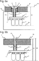
Figure 6a shows a cross section of a display tile according to an embodiment of the invention when the top of the LED is closer thefirst surface 11 ofLED board 1 than nominal -
Figure 6b shows a cross section of a display tile when the top of the LED is closer thefirst surface 11 ofLED board 1 than nominal is not compensated for. -
Figure 7a shows examples of geometries for the adjusting means 6 and theopening 33 according to an embodiment of the invention. -
Figures 7b and 7c show an example of adjusting means 6 where the cross sections in a first part and a second part of the adjusting means are different according to an embodiment of the invention. -
Figures 8a, 8b and8c show a cross section of a display tile according to embodiments of the invention where the adjusting means 6 and 6b compensate for an irregular LED board,spacers -
Figure 9 shows a perspective view and a cross section of an example of adjusting means with an integral fastening means according to an embodiment of the invention. -
Figure 10 shows an example of method to adjust a display tile according to an embodiment of the invention. - The present invention will be described with respect to particular embodiments and with reference to certain drawings but the invention is not limited thereto but only by the claims. The drawings described are only schematic and are nonlimiting. In the drawings, the size of some of the elements may be exaggerated and not drawn on scale for illustrative purposes. The dimensions and the relative dimensions do not correspond to actual reductions to practice of the invention.
- While the description will be done for a LED display, the invention also applies to display tile where an image forming element (e.g. a liquid crystal panel) or a set of image forming elements (e.g. OLED) on a display board must be aligned with a carrier board. In the following any reference to LED (light emitting diode) can be replaced with OLED (organic light emitting diode). In the following a display board will be described with reference to an LED display, and hence the display board will be called LED board, as an example. However, the display board is not limited to an LED board but includes other types of boards such as display boards with OLED emitters.
- A
LED board 1 consists of a printed circuit board (PCB) bearing electrically conducting tracks e.g. copper tracks that connects Light Emitting Diodes 2 (LED) to various electronic components (like e. g. current drivers, power supply contacts etc...). As seen onfigure 1 , TheLED board 1 has afirst face 11 and asecond face 12 that are parallel. The LEDs are mounted on thefirst face 11 of the LED board. The tolerance on the vertical position of theLED 2 with respect to thefirst face 11 is the same for all LEDs mounted on thesame LED board 1. The LEDs can be surface mount devices or through-hole devices. - The
LED board 1 is fastened to acarrier board 3. Thecarrier board 3 will be the mechanical interface between the LED board and asupport structure 4 of atiled display 5. - The
carrier board 3 has afirst face 31 and asecond face 32. Thefirst face 31 and thesecond face 32 are substantially parallel to each other. The distance between thefirst face 31 and thesecond face 32 is the thickness T1 of thecarrier board 3. The first face 31 (the front or front face of the carrier board 3) will be closest to theLED board 1 when theLED board 1 and thecarrier board 3 are assembled. The second face 32 (the back or back face of the carrier board 3) will be closest to thesupport structure 4 when theLED board 1 and its associatedcarrier board 3 are fastened to thesupport structure 4. - The
carrier board 3 has at least oneopening 33 extending from thefirst face 31 to thesecond face 32. Theopening 33 has sidewalls 34 that are preferably perpendicular to thefirst face 31 and thesecond face 32 of thecarrier board 3. The intersection of thesidewalls 34 and thefirst face 31 is a curve C1. C1 is preferably a circle but other curves such as arcuate are possible. - An adjusting means 6 has a
first face 61 and asecond face 62. Thefirst face 61 and thesecond face 62 are preferably substantially parallel to each other. The adjusting means 6 has athird face 63 extending from thefirst face 61 to thesecond face 62. The third face is preferably perpendicular to thefirst face 61 and thesecond face 62. The adjusting means 6 is positioned in theopening 33 in thecarrier board 3, the first face andsecond face second face carrier board 3. For instance, if theopening 33 is cylindrical and the curve C1 is a circle of radius R1 as onfigure 2 , the cross section of the adjusting means 6 is preferably a circle C2 with a radius R2 equal to or slightly smaller than the radius R1. Other cross sections are possible for the adjusting means 6, some examples of which are given onfigure 7a where the curve C1 is a curve or a square. In some cases it may be advantageous that the thickness T2 of the adjusting means 6 is less than the thickness T1 of the carrier board 3 (in particular at the level of the opening 33). - The cross section of the adjusting means 6 by a plane parallel to
first face 61 can vary from thefirst surface 61 to thesecond surface 62. In particular, the cross section of adjusting means 6 can decrease close to the second surface. In particular as illustrated onfigures 7b and 7c , the cross section can have an area equal to that of thefirst surface 61 in a first part of the adjusting means close tofirst surface 61 and can have a second area less than the area ofsurface 61 in a second part of the adjusting means adjacent to surface 62. If theopening 33 determines a circle in thesecond surface 32 of thecarrier board 3, the adjusting means can for instance be the combination of two circular right cylinders: a first cylinder of radius R3 (not shown - slightly smaller than R1) in a first part delimited on one side by thefirst surface 61 and a second cylinder of radius R2 in a second part delimited on one side by thesecond surface 62. - The
space 35 between thesidewall 34 of theopening 3 and thesidewall 63 of the adjusting means 6 along the second part of the adjusting means 6 is thereby larger and it is easier to dispense glue in thespace 35 to fasten the adjusting means to thecarrier board 3. At the same time, the first part of the adjusting means will prevent the glue from spilling onto the spacer and the LED board. It is advantageous to have aspace 35 between to dispense glue on both a portion of thesidewall 34 of theopening 33 and a portion of thesidewall 63 of the adjusting means 6. Indeed, by increasing the surface glued, the fastening of the adjusting means 6 to thecarrier board 3 is improved. - At least one
spacer 7 is fastened to thesecond face 12 of theLED board 1. The position of thespacer 7 corresponds to the position of theopening 33 in thecarrier board 3 when theLED board 1 is positioned parallel to thecarrier board 3, thesecond face 12 of theLED board 1 facing thefirst face 31 of thecarrier board 3. The length ofspacer 7 on different LED boards is less variable than the distance D1 between the top ofLED 2 and thefirst face 11 ofLED board 1 on different LED boards. Thespacer 7 is usually cylindrical and is of the female type, i.e. it has an opening that can accommodate afastening element 8. - At least one
fastening element 8 is used to fasten thecarrier board 3 to theLED board 1. Thefastening element 8 is for instance a screw that fits in theopening 71 of thespacer 7. - As seen on
figure 3 , thefastening element 8 goes through anopening 64 of adjusting means 6 from thesecond face 62 to thefirst face 61, preferably perpendicularly to thefaces opening 64 is preferably unthreaded, thefastening element 8 can move through it without excessive resistance. - A
head 81 of fastening element will stop the progression offastening element 8 through adjusting means 6. For instance, if thefastening element 8 is a screw, the head of the screw will press against thesecond face 62 of the adjusting means 6 and stop the progression of thescrew 8 even if a force is exerted on the screw. - As the
screw 8 is screwed in thefemale spacer 7; thescrew 8 moves closer to thesecond face 12 ofLED board 1. Thescrew 8 has a length such that it can be screwed in thespacer 7 until thefirst face 61 of adjusting means 6 is in contact withspacer 7. For instance, the length L1 of thescrew 8 is less than the thickness T2 of the adjusting means 6 and the length L2 of the female opening of thespacer 7 combined (L1 < T2 + L2). When thescrew 8 cannot go any deeper into thespacer 7, the adjusting means 6 is fastened to thecarrier board 3. This can be done by dispensingglue 9 inside theopening 33, preferably from thesecond surface 32, theglue 9 contacting at least thesecond surface 62 of adjusting means 6 and thesidewall 34 of theopening 33 in thecarrier board 3. Depending on the cross section of adjusting means 6, the glue may go deeper into theopening 33 and contact thesidewalls 63 of adjusting means 6. - Alternatively, the
opening 64 of adjusting means 6 can be threaded and thespacer 7 can have a male threaded part 72 instead of a threadedopening 71. Adjusting means 6 is screwed over the male threaded part 72 until it cannot slide any further into theopening 33.Glue 9 is then dispensed in theopening 33 on thesidewall 34 and thesecond face 62 of adjusting means 6 to fasten thecarrier board 3 and the adjusting means 6 together. - The
glue 9 is chosen in function of the material of thecarrier board 3 and the adjusting means 6. Theglue 9 is preferably a fast curing glue. - There is preferably more than one
spacer 7 distributed evenly across thesecond face 12 of theLED board 1. For eachspacer 7b, there will be acorresponding opening 33b in thecarrier board 3 and a corresponding adjusting means 6b. The position in anopening 33b of the adjusting means 6b associated with aparticular spacer 7b can be the same for all the openings and their associated adjusting means. This will be the case if the thickness of theLED board 1, the thickness of thecarrier board 3 is constant across the board and the length of thespacers spacer - If the thickness of the
LED board 1 and/or thecarrier board 3 is not constant across the board and/or the length of the spacers is not the same for thespacers corresponding opening figure 8a (thickness of the LED board not constant across the board),figure 8b (spacers figure 8c (thickness of the carrier board not constant across the board). The adjusting means 6 can thus compensate for tolerances affecting different components of the display tile. - The area of opening 33 in the
carrier board 3 is preferably larger than the area of a cross section of thespacer 7 by a plane parallel to the first and second faces of the carrier board. This is to ensure that thespacer 7 can penetrate theopening 33 if made necessary by the tolerance on the position of theLED 2 with respect to thefirst surface 11 of theLED board 1. - Alternatively to a screw, the fastening means 8 can be an integral part of the adjusting means 6. As illustrated on
figure 9 , the fastening means 8 can be a threaded extension that extends from thefirst surface 61 of the adjusting means 6 in a direction perpendicular to that surface of the adjusting means 6 to mate with a threaded opening in thespacer 7. Thesecond surface 62 of the adjusting means can then be a driving surface, i.e. it can be slotted, aslot 65 insecond surface 62 allowing interaction of thesecond surface 62 with a tool like a screwdriver. - Alignment of the
LEDs 2 withcarrier board 3 can be facilitated by the use of ajig 10. - The jig has at least a first "bottom" part 10A. The bottom part 10A has a
first surface 101. Thefirst surface 101 has an area sufficient to accommodate all the LED on theLED board 1. - The jig can have a second "top" part 10B. The top part 10B will help position the carrier board with respect to the
LED board 1. - The bottom part 10A has sidewalls 102 extending above its
first surface 101. The rim of thefirst surface 31 of thecarrier board 3 can contact asurface 103 of thesidewalls 102. The distance between thefirst surface 101 of the bottom part 10A and thesecond surface 32 of thecarrier board 3 corresponds to the desired distance D0 between the tops of theLED 2 on theLED board 1 and thesecond surface 32 of thecarrier board 3. In this first embodiment of thejig 10, the distance between thesurface 103 and thefirst surface 101 is equal to the nominal distance DO minus the thickness of thecarrier board 3. - In general, when the tolerance on the thickness of the carrier board is not negligible, a second embodiment of the
jig 10 is used wherein thesidewalls 102 have asecond surface 104 along an outer edge of thesidewalls 102. Thesecond surface 104 is parallel to the first surface 101 (the reference surface). The distance between thesecond surface 104 and thefirst surface 101 is equal to the nominal distance DO desired between the top of theLEDs 2 and thesecond surface 32 of thecarrier board 3. In this case, the distance between thesurface 103 and thefirst surface 101 is less than the nominal distance DO minus the nominal thickness of thecarrier board 3. - An elastic material 105 like e.g. elastomer or rubber covers the
surface 103 of the sidewalls. The thickness of the elastic material 105 is determined in function of its elasticity, the distance between thefirst surface 103 and thesecond surface 104 and the nominal thickness of thecarrier board 3. Once positioned in the jig, thecarrier board 3 is in contact with the elastic material 105 and a force is applied on one or more points of thesecond surface 32 of thecarrier board 3 to bring thesecond surface 32 of the carrier board at the same level as thesecond surface 104 of thesidewall 102. This is evaluated in first instance at the periphery of thecarrier board 3. Alternatively, a top part 10B of thejig 10 is fastened to the bottom part 10A of the jig by means of e.g. screws. Pressure is applied to the carrier board either directly by the top part or by means of screws fitting in threaded openings in the top part. Once thesecond surface 32 of thecarrier board 3 is flush with thesecond surface 104 of the sidewalls, the distance between the top of the LEDs 2 (in contact with the reference surface 101) and thesecond surface 32 of thecarrier board 3 is equal to the nominal or desired distance. Openings in the top part 10B of the jig permit access to theopenings carrier board 3. - The method of assembling the
LED board 1 to thecarrier board 3 in order to obtain the desired distance between the top of theLED 2 and thesecond surface 32 of thecarrier board 3 will now be detailed. An example of the method is given onfigure 10 . - In a first step S10 the tops of
LEDs 2 on theLED board 1 are positioned in afirst reference plane 101. - With help of the
jig 10, this is done by positioning theLED board 1 on the bottom part 10A of theJIG 10 with the tops ofLEDs 2 in contact with thefirst surface 101. - In a second step S20, the openings (33, 33b ...) in the carrier board are aligned with the spacers (7, 7b ...).
- In a third step S30, the
second surface 32 of thecarrier board 3 is positioned in asecond reference plane 104; thefirst surface 31 of thecarrier board 3 facing thesecond surface 12 of the LED board. The first and second reference planes are parallel and the distance between the first and second reference plane is equal to a nominal distance D0. - When using the first embodiment of the jig, positioning the
second surface 32 of the carrier board in the second reference plane in step S20 is done by bringing thefirst surface 31 of the carrier board in contact with thesurface 103 of thesidewall 102. - When using the second embodiment of the
jig 10, thefirst surface 31 of thecarrier board 3 is brought into contact with the elastic material 105 and pressure is applied to the carrier board until thesecond surface 32 of the carrier board in the second reference plane corresponding to thesecond surface 104 of thesidewall 102 of the jig. -
Steps 20 and 30 can be interchanged. For instance when only part 10A is used, the carrier board can first be positioned on thesurface 103 to be at the correct distance and then slid in the plane ofsurface 103 to alignopenings spacers - In a fourth step S40, an adjusting means 6 is positioned in the
opening 33 and moved in the opening in a direction perpendicular to thesecond surface 32 until afirst surface 61 of the adjusting means contacts aspacer 7. This operation is repeated for everyspacer 7 that can be accessed by anopening 33 in the carrier board. - In a fifth step S50, the adjusting means 6 is fastened to the
spacer 7. This operation is repeated for everyspacer 7 that can be accessed by anopening 33 in the carrier board. - When using e.g. a
screw 8 to fasten the adjusting means 6 to thespacer 7, theopening 71 in thespacer 7 and theopening 64 in adjusting means 6 are aligned.Screw 8 is engaged inopening 64 and screwed in threadedopening 71 of thespacer 7 until thehead 81 ofscrew 8 contacts thesecond surface 62 of adjusting means 6 and presses adjusting means 6 against thespacer 7. - In a sixth step S60, the adjusting means 6 is fastened to the
carrier board 3. This can be done by dispensingglue 9 in theopening 33 of the carrier board. The operation is repeated for each spacer on theLED board 1 facing an opening in thecarrier board 3. - The distance between the tops of the LEDs and the second face of the carrier board is now fixed and equal to DO.
- Alternatively, step S50 and step S60 can be interchanged. In particular, when the fastening means 8 is an integral part of the adjusting means as is the case on
figure 9 ; thefirst surface 61 of the adjusting means 6 will come in contact with thespacer 7 after the fastening means 8 is completely engaged in the threaded opening ofspacer 7. In other words, thefirst surface 61 will contact thespacer 7 as a result of fastening the adjusting means 6 to thespacer 7. - If glue is used to fasten the adjusting means to the carrier board and if a screw going through an
opening 64 of the adjusting means is used to fasten the adjusting means and the spacer, it may be advantageous to fasten the adjusting means and the spacer before dispensing the glue. Indeed, in that case, theopening 64 being then obstructed by thescrew 8, theglue 9 will not spill into theopening 64. -
Figure 4 to Figure 6 show three typical situations and the resulting position of the adjusting means 6 to fastenLED board 1 tocarrier board 3. - In
figure 4 , the tops of theLEDs 2 are at a nominal distance from thefirst surface 11 ofLED board 1. - In
Figure 5a , the tops of theLEDs 2 are farther away from thefirst surface 11 ofLED board 1 than nominal (nominal distance between the LED body and the LED board is figured as ND onfigures 4 to 6b ). - If nothing were done about it (as on
figure 5b ), where the carrier board and the LED board are fastened together without the help of adjusting means 6, fastening theLED board 1 to thecarrier board 3 without the adjusting means 6 would lead to a distance D1 between the back of thecarrier board 3 and the tops ofLEDs 2 larger than the desired distance DO. - The difference between D1 and DO can be compensated for by the adjusting means 6 as follows: the
spacer 7 can enter theopening 33; and the adjusting means 6 sliding intoopening 33 follows thespacer 7 thereby compensating for the difference between the actual and nominal position of theLED 2 above thefirst surface 12 of the LED board. The position of adjusting means 6 is fixed with glue and the distance between the top of theLED 2 and theback 32 of thecarrier board 3 is the desired DO. - In
Figure 6a , the tops of theLEDs 2 are closer to thefirst surface 11 ofLED board 1 than a nominal distance. - If nothing were done about it as on
figure 6b , fastening theLED board 1 to thecarrier board 3 without the adjusting means 6 would lead to a distance D1 between the back of thecarrier board 3 and the top ofLED 2 smaller than the desired distance D0. - The difference between D1 and D0 can be compensated for by the adjusting means 6 as follows: the
spacer 7 does not intersect the plane of thefirst surface 31 of thecarrier board 3 and the adjusting means 6 comes partially out of opening 33 (thefirst surface 61 is below the first surface 31) and stops when it contacts thespacer 7 compensating for the difference between the actual and nominal position of theLED 2 above thefirst surface 12 of the LED board. The position of adjusting means 6 is fixed with glue and the distance between the top of theLED 2 and the back of thecarrier board 3 is the desired DO. - The
LED board 1 can warp during manufacturing or manipulation. To compensate for this, pressure can be applied at several points of thesecond surface 12 ofLED board 1 when it is positioned in ajig 10. - The top part 10B of the
jig 10 is fastened to the bottom part 10A e.g. by means of screws. At least one threadedcomponent 11 e.g. screws with a blunt end can be screwed through threaded openings in the top part 10B and pass through openings in thecarrier board 3. The blunt ends 110 of the threadedcomponents 11 straighten a warped LED board by applying pressure on at least one point of theLED board 1 and preferably 4 non collinear points of thesecond surface 12 of theLED board 1.
Claims (14)
- A display tile comprising a display board (1) and a carrier board (3), LED's (2) being mounted on a first surface (11) of the display board (1) and the carrier board being for attachment to a frame, the display board (1) and the carrier board (3) being fastened together by the intermediary of a spacer (7, 7b) characterised in that the display tile further comprises an adjusting means (6, 6b) positioned between the spacer (7, 7b) and the carrier board (3) wherein the adjusting means (6, 6b) is adapted to engage in an opening (33, 33b) in the carrier board (3), the adjusting means (6, 6b) is adapted to allow a compensation of the tolerances affecting the position of the LED's with respect to the carrier board (3) in a direction perpendicular to the carrier board (3) whereby the compensation is obtained by the position of the adjusting means (6, 6b) in their corresponding opening (33, 33b), wherein the adjusting means (6, 6b) is adapted for adjusting a relative position of the tops of the LEDs (2) with respect to a carrier board (3), and wherein the distance between a first surface (61) of the adjusting means (6, 6b) and a first surface (31) of the carrier board (3) is set to the difference between a nominal distance (D0) and the sum of the distance between the tops of LEDs (2) on the display board (1) and a second surface (12) of the display board (1), the length of the spacer (7, 7b) and the thickness T1 of the carrier board (3), wherein the nominal distance (D0) is the distance between the top of the LEDs and the second surface (32) or back of the carrier board (3).
- A display tile according to claim 1, wherein a sidewall (34) of the opening (33, 33b) in the carrier board (3) is perpendicular to the second surface (32) of the carrier board (3).
- A display tile according to any of the preceding claims, wherein a sidewall (63) of the adjusting means (6, 6b) is parallel to the sidewall (34) of the opening (33, 33b) in the carrier board (3).
- A display tile according to any of the preceding claims, wherein the thickness T2 of the adjusting means (6, 6b) is less than the thickness T1 of the carrier board (3).
- A display tile according to any of the preceding claims, wherein the cross section of the adjusting means (6, 6b) fits in the opening (33, 33b), or wherein the cross section of the adjusting means (6, 6b) has a first area in a first part of the adjusting means (6, 6b) and a second area in a second part of the adjusting means (6, 6b).
- A display tile according to any previous claim, wherein the adjusting means (6, 6b) has a first part that is a circular right cylinder with a first radius and a second part that is a circular right cylinder with a second radius smaller than the first radius, or
wherein the adjusting means (6) is fastened to the carrier board (3) by glue (9) extending on a second surface (62) and/or a sidewall (63) of the adjusting means (6, 6b) and a sidewall (34) of the opening (33). - A display tile according to any of the preceding claims, wherein a fastening means (8) fastens the adjusting means (6, 6b) to the spacer (7, 7b).
- A display tile according to claim 7, wherein the fastening means (8) goes through an opening (64) in the adjusting means (6,6b), or is a screw.
- A display tile according to any of claims 1 to 8, wherein a threaded extension extends from a first surface (61) of the adjusting means (6, 6b) and that the spacer (7, 7b) has a matching threaded opening to receive the threaded extension.
- A display tile according to claim 9, wherein the second surface (62) of the adjusting means (6, 6b) is a driving surface.
- A method to adjust the distance between the tops of the LEDs (2) on a first surface (11) of the display board (1) and the back surface (32) of the carrier board (3) of the display tile of claim 1, the method comprising the steps:- positioning the tops of the LEDs (2) on a display board (1) in a first reference plane (101),- aligning openings (33, 33b) in the carrier board (3) with spacers (7, 7b) distributed on the display board (1),- positioning a second surface (32) of a carrier board (3) in a second reference plane (104); a first surface (11) of the carrier board (3) facing a second surface (12) of the LED display (1); the first (101) and second (104) reference planes being parallel and the distance between the first (101) and second (104) reference planes being equal to a desired nominal distance (D0),- providing adjusting means (6, 6b) for adjusting a relative position of the tops of the LEDs (2) with respect to the carrier board (3),- moving the adjusting means (6, 6b) in the openings (33, 33b) until a first surface (61, 61b) of each adjusting means (6, 6b) contacts a spacer (7, 7b),- fastening each adjusting means (6, 6b) to its corresponding spacer (7, 7b),- fastening the adjusting means (6, 6b) to the carrier board (3).
- The method of claim 11, wherein glue is dispensed in the openings (33, 33b), on a sidewall (34) of the openings (33, 33b) and on a second surface (62) of the adjusting means (6, 6b).
- The method of claim 12, wherein the glue is allowed to harden, to set or to cure to fasten the adjusting means (6, 6b) to the carrier board (3) at the position where the adjusting means (6, 6b) compensates for the tolerances affecting the position of the LEDs (2) with respect to the carrier board (3) in a direction perpendicular to the carrier board (3).
- A tiled display apparatus comprising a plurality of display tiles according to any of the claims 1 to 10 fixed to a frame.
Applications Claiming Priority (2)
| Application Number | Priority Date | Filing Date | Title |
|---|---|---|---|
| GB1410637.1A GB2527131A (en) | 2014-06-13 | 2014-06-13 | Adjustable display tile for tiled display |
| PCT/EP2015/063150 WO2015189377A1 (en) | 2014-06-13 | 2015-06-12 | Adjustable display tile for tiled display |
Publications (2)
| Publication Number | Publication Date |
|---|---|
| EP3155606A1 EP3155606A1 (en) | 2017-04-19 |
| EP3155606B1 true EP3155606B1 (en) | 2021-11-03 |
Family
ID=51266609
Family Applications (1)
| Application Number | Title | Priority Date | Filing Date |
|---|---|---|---|
| EP15733647.0A Active EP3155606B1 (en) | 2014-06-13 | 2015-06-12 | Adjustable display tile for tiled display |
Country Status (6)
| Country | Link |
|---|---|
| US (2) | US9886877B2 (en) |
| EP (1) | EP3155606B1 (en) |
| CN (1) | CN106463081B (en) |
| BE (1) | BE1023214A1 (en) |
| GB (1) | GB2527131A (en) |
| WO (1) | WO2015189377A1 (en) |
Families Citing this family (14)
| Publication number | Priority date | Publication date | Assignee | Title |
|---|---|---|---|---|
| GB201502203D0 (en) * | 2015-02-10 | 2015-03-25 | Barco Nv | Load levelling apparatus for tiled displays |
| KR102445232B1 (en) | 2016-10-06 | 2022-09-21 | 아이맥스 시어터스 인터내셔널 리미티드 | Cinema light emitting screen and sound system |
| EP3642825A1 (en) | 2017-06-20 | 2020-04-29 | IMAX Theatres International Limited | Active display with reduced screen-door effect |
| EP3669349A1 (en) | 2017-08-18 | 2020-06-24 | Barco N.V. | Adjustable support structure for display tile |
| US11682369B2 (en) | 2017-09-20 | 2023-06-20 | Imax Theatres International Limited | Light emitting display with tiles and data processing |
| KR102541526B1 (en) * | 2018-07-27 | 2023-06-09 | 삼성전자주식회사 | Display apparatus and manufacturing method thereof |
| CA3121343A1 (en) | 2018-11-29 | 2020-06-04 | Barco N.V. | Alignment for tiles of tiled displays |
| CN113228142B (en) * | 2018-12-21 | 2023-10-31 | 巴科股份有限公司 | Display block for tiled display with improved flatness |
| CN110444127B (en) * | 2019-08-08 | 2021-12-31 | 深圳市洲明科技股份有限公司 | Display screen and assembling method thereof |
| US20230009971A1 (en) * | 2019-11-20 | 2023-01-12 | Lg Display Co., Ltd. | Display device |
| CN110827709B (en) * | 2019-11-26 | 2023-05-23 | 苏州佳世达电通有限公司 | Display module |
| CN111308747B (en) * | 2020-03-17 | 2023-09-22 | 北京七星华创集成电路装备有限公司 | Display panel bearing workbench and liquid crystal display production equipment |
| US20220198969A1 (en) * | 2020-05-28 | 2022-06-23 | Beijing Boe Optoelectronics Technology Co., Ltd. | Display device and manufacturing method thereof |
| WO2021255203A2 (en) * | 2020-06-18 | 2021-12-23 | Barco N.V. | System and method for connecting display panels |
Citations (1)
| Publication number | Priority date | Publication date | Assignee | Title |
|---|---|---|---|---|
| US5805117A (en) * | 1994-05-12 | 1998-09-08 | Samsung Electronics Co., Ltd. | Large area tiled modular display system |
Family Cites Families (16)
| Publication number | Priority date | Publication date | Assignee | Title |
|---|---|---|---|---|
| JPH01297696A (en) * | 1988-05-26 | 1989-11-30 | Koito Ind Ltd | Information display device |
| US6150996A (en) | 1998-08-26 | 2000-11-21 | Addco, Inc. | Changeable message sign system with reconfigurable sign screen |
| US20020122134A1 (en) * | 2001-03-05 | 2002-09-05 | Kalua Kevin A. | Video display array of sealed, modular units |
| US20030016227A1 (en) * | 2001-07-19 | 2003-01-23 | Matthies Dennis L. | Adaptable large area display |
| US6813853B1 (en) * | 2002-02-25 | 2004-11-09 | Daktronics, Inc. | Sectional display system |
| US7231734B2 (en) * | 2003-02-03 | 2007-06-19 | Luminator Holding, L.P. | Display device with rail support |
| JP4269748B2 (en) * | 2003-04-01 | 2009-05-27 | セイコーエプソン株式会社 | Manufacturing method of display device |
| US20080266206A1 (en) * | 2005-03-11 | 2008-10-30 | Adaptive Mocro Systems Llc | Modular System for a Display Panel Assembly |
| US7959325B2 (en) * | 2005-11-18 | 2011-06-14 | Cree, Inc. | Solid state lighting units and methods of forming solid state lighting units |
| GB0711626D0 (en) * | 2007-06-18 | 2007-07-25 | Barco Nv | Support for direct light displays |
| US8384616B2 (en) | 2008-04-15 | 2013-02-26 | Barco, Inc. | Isolating alignment and structural strength in LED display systems |
| US8171690B2 (en) * | 2008-05-28 | 2012-05-08 | 3Form, Inc. | Countersunk fastener assemblies, panel mounting systems, and methods |
| CN201226214Y (en) | 2008-06-06 | 2009-04-22 | 上海大峡谷光电科技有限公司 | Novel structure for LED display screen |
| US20120181402A1 (en) * | 2011-01-13 | 2012-07-19 | 3Form, Inc. | Adjustable bushing assemblies, panel mounting systems, and methods |
| CN202905058U (en) * | 2012-11-08 | 2013-04-24 | 上海三思电子工程有限公司 | Mounting structure of display modules |
| US8840284B1 (en) * | 2013-05-01 | 2014-09-23 | Revolution Display, Inc. | Modular light emitting displays and arrays of same |
-
2014
- 2014-06-13 GB GB1410637.1A patent/GB2527131A/en not_active Withdrawn
-
2015
- 2015-06-11 BE BE20150169A patent/BE1023214A1/en unknown
- 2015-06-12 US US15/317,761 patent/US9886877B2/en active Active
- 2015-06-12 CN CN201580031641.6A patent/CN106463081B/en active Active
- 2015-06-12 EP EP15733647.0A patent/EP3155606B1/en active Active
- 2015-06-12 WO PCT/EP2015/063150 patent/WO2015189377A1/en active Application Filing
-
2018
- 2018-02-02 US US15/886,924 patent/US20180233072A1/en not_active Abandoned
Patent Citations (1)
| Publication number | Priority date | Publication date | Assignee | Title |
|---|---|---|---|---|
| US5805117A (en) * | 1994-05-12 | 1998-09-08 | Samsung Electronics Co., Ltd. | Large area tiled modular display system |
Also Published As
| Publication number | Publication date |
|---|---|
| GB2527131A (en) | 2015-12-16 |
| CN106463081B (en) | 2019-07-23 |
| BE1023214A1 (en) | 2016-12-21 |
| EP3155606A1 (en) | 2017-04-19 |
| GB201410637D0 (en) | 2014-07-30 |
| US9886877B2 (en) | 2018-02-06 |
| WO2015189377A1 (en) | 2015-12-17 |
| CN106463081A (en) | 2017-02-22 |
| US20170116895A1 (en) | 2017-04-27 |
| US20180233072A1 (en) | 2018-08-16 |
Similar Documents
| Publication | Publication Date | Title |
|---|---|---|
| EP3155606B1 (en) | Adjustable display tile for tiled display | |
| CN108370650B (en) | Printed circuit board mounting structure and display device including the same | |
| US10353138B2 (en) | Display device and method for fabricating the same | |
| US9323087B2 (en) | Display apparatus and television receiver | |
| KR101377005B1 (en) | Top chassis, liquid crystal display including the same and assembly method thereof | |
| CN104347010B (en) | Bottom and use the display device of this bottom | |
| US7649588B2 (en) | Positioning structure for sheet-shaped component and display device using same | |
| US11353732B2 (en) | Display apparatus | |
| KR20200023188A (en) | Display appartus | |
| KR20180001949A (en) | Display device | |
| US20070139872A1 (en) | Display device assembly | |
| US20100201906A1 (en) | Liquid crystal display device and manufacturing method thereof | |
| US11026328B2 (en) | Display apparatus and manufacturing method thereof | |
| KR102590119B1 (en) | Display apparatus | |
| KR20070049417A (en) | Liquid crystal module | |
| US9606385B2 (en) | Display device | |
| CN114999336A (en) | Sub-display panel assembly and splicing display device | |
| US11627672B2 (en) | Display apparatus including frame for supporting printed circuit board | |
| JP2006243469A (en) | Device and method for fitting display panel | |
| KR20150066324A (en) | Liquid crystal display and method fo manufacturing the same | |
| KR20070050667A (en) | Bottom chassis for flat panel display and method for attaching flexible printed circuit board using the same | |
| CN112349212A (en) | Display module, display panel and display device | |
| KR101788871B1 (en) | Liquid crystal display device | |
| KR20110080044A (en) | Method for driving the backlight unit and display apparatus thereof | |
| KR20110015091A (en) | A backlight unit, method for driving the backlight unit and display apparatus thereof |
Legal Events
| Date | Code | Title | Description |
|---|---|---|---|
| STAA | Information on the status of an ep patent application or granted ep patent |
Free format text: STATUS: THE INTERNATIONAL PUBLICATION HAS BEEN MADE |
|
| PUAI | Public reference made under article 153(3) epc to a published international application that has entered the european phase |
Free format text: ORIGINAL CODE: 0009012 |
|
| STAA | Information on the status of an ep patent application or granted ep patent |
Free format text: STATUS: REQUEST FOR EXAMINATION WAS MADE |
|
| 17P | Request for examination filed |
Effective date: 20170113 |
|
| AK | Designated contracting states |
Kind code of ref document: A1 Designated state(s): AL AT BE BG CH CY CZ DE DK EE ES FI FR GB GR HR HU IE IS IT LI LT LU LV MC MK MT NL NO PL PT RO RS SE SI SK SM TR |
|
| AX | Request for extension of the european patent |
Extension state: BA ME |
|
| DAV | Request for validation of the european patent (deleted) | ||
| DAX | Request for extension of the european patent (deleted) | ||
| STAA | Information on the status of an ep patent application or granted ep patent |
Free format text: STATUS: EXAMINATION IS IN PROGRESS |
|
| 17Q | First examination report despatched |
Effective date: 20180731 |
|
| STAA | Information on the status of an ep patent application or granted ep patent |
Free format text: STATUS: EXAMINATION IS IN PROGRESS |
|
| GRAP | Despatch of communication of intention to grant a patent |
Free format text: ORIGINAL CODE: EPIDOSNIGR1 |
|
| STAA | Information on the status of an ep patent application or granted ep patent |
Free format text: STATUS: GRANT OF PATENT IS INTENDED |
|
| INTG | Intention to grant announced |
Effective date: 20210519 |
|
| GRAS | Grant fee paid |
Free format text: ORIGINAL CODE: EPIDOSNIGR3 |
|
| GRAA | (expected) grant |
Free format text: ORIGINAL CODE: 0009210 |
|
| STAA | Information on the status of an ep patent application or granted ep patent |
Free format text: STATUS: THE PATENT HAS BEEN GRANTED |
|
| AK | Designated contracting states |
Kind code of ref document: B1 Designated state(s): AL AT BE BG CH CY CZ DE DK EE ES FI FR GB GR HR HU IE IS IT LI LT LU LV MC MK MT NL NO PL PT RO RS SE SI SK SM TR |
|
| REG | Reference to a national code |
Ref country code: GB Ref legal event code: FG4D |
|
| REG | Reference to a national code |
Ref country code: AT Ref legal event code: REF Ref document number: 1444686 Country of ref document: AT Kind code of ref document: T Effective date: 20211115 Ref country code: CH Ref legal event code: EP |
|
| REG | Reference to a national code |
Ref country code: DE Ref legal event code: R096 Ref document number: 602015074660 Country of ref document: DE |
|
| REG | Reference to a national code |
Ref country code: IE Ref legal event code: FG4D |
|
| REG | Reference to a national code |
Ref country code: LT Ref legal event code: MG9D |
|
| REG | Reference to a national code |
Ref country code: NL Ref legal event code: MP Effective date: 20211103 |
|
| REG | Reference to a national code |
Ref country code: AT Ref legal event code: MK05 Ref document number: 1444686 Country of ref document: AT Kind code of ref document: T Effective date: 20211103 |
|
| PG25 | Lapsed in a contracting state [announced via postgrant information from national office to epo] |
Ref country code: RS Free format text: LAPSE BECAUSE OF FAILURE TO SUBMIT A TRANSLATION OF THE DESCRIPTION OR TO PAY THE FEE WITHIN THE PRESCRIBED TIME-LIMIT Effective date: 20211103 Ref country code: LT Free format text: LAPSE BECAUSE OF FAILURE TO SUBMIT A TRANSLATION OF THE DESCRIPTION OR TO PAY THE FEE WITHIN THE PRESCRIBED TIME-LIMIT Effective date: 20211103 Ref country code: FI Free format text: LAPSE BECAUSE OF FAILURE TO SUBMIT A TRANSLATION OF THE DESCRIPTION OR TO PAY THE FEE WITHIN THE PRESCRIBED TIME-LIMIT Effective date: 20211103 Ref country code: BG Free format text: LAPSE BECAUSE OF FAILURE TO SUBMIT A TRANSLATION OF THE DESCRIPTION OR TO PAY THE FEE WITHIN THE PRESCRIBED TIME-LIMIT Effective date: 20220203 Ref country code: AT Free format text: LAPSE BECAUSE OF FAILURE TO SUBMIT A TRANSLATION OF THE DESCRIPTION OR TO PAY THE FEE WITHIN THE PRESCRIBED TIME-LIMIT Effective date: 20211103 |
|
| PG25 | Lapsed in a contracting state [announced via postgrant information from national office to epo] |
Ref country code: IS Free format text: LAPSE BECAUSE OF FAILURE TO SUBMIT A TRANSLATION OF THE DESCRIPTION OR TO PAY THE FEE WITHIN THE PRESCRIBED TIME-LIMIT Effective date: 20220303 Ref country code: SE Free format text: LAPSE BECAUSE OF FAILURE TO SUBMIT A TRANSLATION OF THE DESCRIPTION OR TO PAY THE FEE WITHIN THE PRESCRIBED TIME-LIMIT Effective date: 20211103 Ref country code: PT Free format text: LAPSE BECAUSE OF FAILURE TO SUBMIT A TRANSLATION OF THE DESCRIPTION OR TO PAY THE FEE WITHIN THE PRESCRIBED TIME-LIMIT Effective date: 20220303 Ref country code: PL Free format text: LAPSE BECAUSE OF FAILURE TO SUBMIT A TRANSLATION OF THE DESCRIPTION OR TO PAY THE FEE WITHIN THE PRESCRIBED TIME-LIMIT Effective date: 20211103 Ref country code: NO Free format text: LAPSE BECAUSE OF FAILURE TO SUBMIT A TRANSLATION OF THE DESCRIPTION OR TO PAY THE FEE WITHIN THE PRESCRIBED TIME-LIMIT Effective date: 20220203 Ref country code: NL Free format text: LAPSE BECAUSE OF FAILURE TO SUBMIT A TRANSLATION OF THE DESCRIPTION OR TO PAY THE FEE WITHIN THE PRESCRIBED TIME-LIMIT Effective date: 20211103 Ref country code: LV Free format text: LAPSE BECAUSE OF FAILURE TO SUBMIT A TRANSLATION OF THE DESCRIPTION OR TO PAY THE FEE WITHIN THE PRESCRIBED TIME-LIMIT Effective date: 20211103 Ref country code: HR Free format text: LAPSE BECAUSE OF FAILURE TO SUBMIT A TRANSLATION OF THE DESCRIPTION OR TO PAY THE FEE WITHIN THE PRESCRIBED TIME-LIMIT Effective date: 20211103 Ref country code: GR Free format text: LAPSE BECAUSE OF FAILURE TO SUBMIT A TRANSLATION OF THE DESCRIPTION OR TO PAY THE FEE WITHIN THE PRESCRIBED TIME-LIMIT Effective date: 20220204 Ref country code: ES Free format text: LAPSE BECAUSE OF FAILURE TO SUBMIT A TRANSLATION OF THE DESCRIPTION OR TO PAY THE FEE WITHIN THE PRESCRIBED TIME-LIMIT Effective date: 20211103 |
|
| PG25 | Lapsed in a contracting state [announced via postgrant information from national office to epo] |
Ref country code: SM Free format text: LAPSE BECAUSE OF FAILURE TO SUBMIT A TRANSLATION OF THE DESCRIPTION OR TO PAY THE FEE WITHIN THE PRESCRIBED TIME-LIMIT Effective date: 20211103 Ref country code: SK Free format text: LAPSE BECAUSE OF FAILURE TO SUBMIT A TRANSLATION OF THE DESCRIPTION OR TO PAY THE FEE WITHIN THE PRESCRIBED TIME-LIMIT Effective date: 20211103 Ref country code: RO Free format text: LAPSE BECAUSE OF FAILURE TO SUBMIT A TRANSLATION OF THE DESCRIPTION OR TO PAY THE FEE WITHIN THE PRESCRIBED TIME-LIMIT Effective date: 20211103 Ref country code: EE Free format text: LAPSE BECAUSE OF FAILURE TO SUBMIT A TRANSLATION OF THE DESCRIPTION OR TO PAY THE FEE WITHIN THE PRESCRIBED TIME-LIMIT Effective date: 20211103 Ref country code: DK Free format text: LAPSE BECAUSE OF FAILURE TO SUBMIT A TRANSLATION OF THE DESCRIPTION OR TO PAY THE FEE WITHIN THE PRESCRIBED TIME-LIMIT Effective date: 20211103 Ref country code: CZ Free format text: LAPSE BECAUSE OF FAILURE TO SUBMIT A TRANSLATION OF THE DESCRIPTION OR TO PAY THE FEE WITHIN THE PRESCRIBED TIME-LIMIT Effective date: 20211103 |
|
| REG | Reference to a national code |
Ref country code: DE Ref legal event code: R097 Ref document number: 602015074660 Country of ref document: DE |
|
| PLBE | No opposition filed within time limit |
Free format text: ORIGINAL CODE: 0009261 |
|
| STAA | Information on the status of an ep patent application or granted ep patent |
Free format text: STATUS: NO OPPOSITION FILED WITHIN TIME LIMIT |
|
| 26N | No opposition filed |
Effective date: 20220804 |
|
| PG25 | Lapsed in a contracting state [announced via postgrant information from national office to epo] |
Ref country code: AL Free format text: LAPSE BECAUSE OF FAILURE TO SUBMIT A TRANSLATION OF THE DESCRIPTION OR TO PAY THE FEE WITHIN THE PRESCRIBED TIME-LIMIT Effective date: 20211103 |
|
| PG25 | Lapsed in a contracting state [announced via postgrant information from national office to epo] |
Ref country code: SI Free format text: LAPSE BECAUSE OF FAILURE TO SUBMIT A TRANSLATION OF THE DESCRIPTION OR TO PAY THE FEE WITHIN THE PRESCRIBED TIME-LIMIT Effective date: 20211103 |
|
| PG25 | Lapsed in a contracting state [announced via postgrant information from national office to epo] |
Ref country code: MC Free format text: LAPSE BECAUSE OF FAILURE TO SUBMIT A TRANSLATION OF THE DESCRIPTION OR TO PAY THE FEE WITHIN THE PRESCRIBED TIME-LIMIT Effective date: 20211103 |
|
| REG | Reference to a national code |
Ref country code: CH Ref legal event code: PL |
|
| PG25 | Lapsed in a contracting state [announced via postgrant information from national office to epo] |
Ref country code: LU Free format text: LAPSE BECAUSE OF NON-PAYMENT OF DUE FEES Effective date: 20220612 Ref country code: LI Free format text: LAPSE BECAUSE OF NON-PAYMENT OF DUE FEES Effective date: 20220630 Ref country code: IE Free format text: LAPSE BECAUSE OF NON-PAYMENT OF DUE FEES Effective date: 20220612 Ref country code: CH Free format text: LAPSE BECAUSE OF NON-PAYMENT OF DUE FEES Effective date: 20220630 |
|
| PG25 | Lapsed in a contracting state [announced via postgrant information from national office to epo] |
Ref country code: IT Free format text: LAPSE BECAUSE OF FAILURE TO SUBMIT A TRANSLATION OF THE DESCRIPTION OR TO PAY THE FEE WITHIN THE PRESCRIBED TIME-LIMIT Effective date: 20211103 |
|
| PGFP | Annual fee paid to national office [announced via postgrant information from national office to epo] |
Ref country code: FR Payment date: 20230630 Year of fee payment: 9 Ref country code: DE Payment date: 20230620 Year of fee payment: 9 |
|
| PGFP | Annual fee paid to national office [announced via postgrant information from national office to epo] |
Ref country code: BE Payment date: 20230613 Year of fee payment: 9 |
|
| PGFP | Annual fee paid to national office [announced via postgrant information from national office to epo] |
Ref country code: GB Payment date: 20230622 Year of fee payment: 9 |
|
| PGFP | Annual fee paid to national office [announced via postgrant information from national office to epo] |
Ref country code: FR Payment date: 20230721 Year of fee payment: 9 |
|
| PG25 | Lapsed in a contracting state [announced via postgrant information from national office to epo] |
Ref country code: HU Free format text: LAPSE BECAUSE OF FAILURE TO SUBMIT A TRANSLATION OF THE DESCRIPTION OR TO PAY THE FEE WITHIN THE PRESCRIBED TIME-LIMIT; INVALID AB INITIO Effective date: 20150612 |