EP3154191A1 - Drive circuit for an oscillator - Google Patents
Drive circuit for an oscillator Download PDFInfo
- Publication number
- EP3154191A1 EP3154191A1 EP15189081.1A EP15189081A EP3154191A1 EP 3154191 A1 EP3154191 A1 EP 3154191A1 EP 15189081 A EP15189081 A EP 15189081A EP 3154191 A1 EP3154191 A1 EP 3154191A1
- Authority
- EP
- European Patent Office
- Prior art keywords
- oscillator
- terminal
- drive circuit
- circuit
- inductor
- Prior art date
- Legal status (The legal status is an assumption and is not a legal conclusion. Google has not performed a legal analysis and makes no representation as to the accuracy of the status listed.)
- Granted
Links
- 239000003990 capacitor Substances 0.000 claims description 17
- 238000000034 method Methods 0.000 claims description 4
- 230000001419 dependent effect Effects 0.000 claims description 3
- 230000005669 field effect Effects 0.000 claims 2
- 239000013078 crystal Substances 0.000 description 51
- 238000010586 diagram Methods 0.000 description 8
- 230000010355 oscillation Effects 0.000 description 7
- 230000007704 transition Effects 0.000 description 2
- 238000007599 discharging Methods 0.000 description 1
- 230000003071 parasitic effect Effects 0.000 description 1
- 239000010453 quartz Substances 0.000 description 1
- 239000004065 semiconductor Substances 0.000 description 1
- VYPSYNLAJGMNEJ-UHFFFAOYSA-N silicon dioxide Inorganic materials O=[Si]=O VYPSYNLAJGMNEJ-UHFFFAOYSA-N 0.000 description 1
Images

Classifications
-
- H—ELECTRICITY
- H03—ELECTRONIC CIRCUITRY
- H03B—GENERATION OF OSCILLATIONS, DIRECTLY OR BY FREQUENCY-CHANGING, BY CIRCUITS EMPLOYING ACTIVE ELEMENTS WHICH OPERATE IN A NON-SWITCHING MANNER; GENERATION OF NOISE BY SUCH CIRCUITS
- H03B5/00—Generation of oscillations using amplifier with regenerative feedback from output to input
- H03B5/30—Generation of oscillations using amplifier with regenerative feedback from output to input with frequency-determining element being electromechanical resonator
- H03B5/32—Generation of oscillations using amplifier with regenerative feedback from output to input with frequency-determining element being electromechanical resonator being a piezoelectric resonator
-
- H—ELECTRICITY
- H03—ELECTRONIC CIRCUITRY
- H03H—IMPEDANCE NETWORKS, e.g. RESONANT CIRCUITS; RESONATORS
- H03H9/00—Networks comprising electromechanical or electro-acoustic devices; Electromechanical resonators
- H03H9/02—Details
- H03H9/125—Driving means, e.g. electrodes, coils
- H03H9/13—Driving means, e.g. electrodes, coils for networks consisting of piezoelectric or electrostrictive materials
-
- H—ELECTRICITY
- H03—ELECTRONIC CIRCUITRY
- H03B—GENERATION OF OSCILLATIONS, DIRECTLY OR BY FREQUENCY-CHANGING, BY CIRCUITS EMPLOYING ACTIVE ELEMENTS WHICH OPERATE IN A NON-SWITCHING MANNER; GENERATION OF NOISE BY SUCH CIRCUITS
- H03B5/00—Generation of oscillations using amplifier with regenerative feedback from output to input
- H03B5/30—Generation of oscillations using amplifier with regenerative feedback from output to input with frequency-determining element being electromechanical resonator
- H03B5/32—Generation of oscillations using amplifier with regenerative feedback from output to input with frequency-determining element being electromechanical resonator being a piezoelectric resonator
- H03B5/36—Generation of oscillations using amplifier with regenerative feedback from output to input with frequency-determining element being electromechanical resonator being a piezoelectric resonator active element in amplifier being semiconductor device
- H03B5/364—Generation of oscillations using amplifier with regenerative feedback from output to input with frequency-determining element being electromechanical resonator being a piezoelectric resonator active element in amplifier being semiconductor device the amplifier comprising field effect transistors
-
- G—PHYSICS
- G04—HOROLOGY
- G04C—ELECTROMECHANICAL CLOCKS OR WATCHES
- G04C3/00—Electromechanical clocks or watches independent of other time-pieces and in which the movement is maintained by electric means
- G04C3/08—Electromechanical clocks or watches independent of other time-pieces and in which the movement is maintained by electric means wherein movement is regulated by a mechanical oscillator other than a pendulum or balance, e.g. by a tuning fork, e.g. electrostatically
- G04C3/12—Electromechanical clocks or watches independent of other time-pieces and in which the movement is maintained by electric means wherein movement is regulated by a mechanical oscillator other than a pendulum or balance, e.g. by a tuning fork, e.g. electrostatically driven by piezoelectric means; driven by magneto-strictive means
-
- H—ELECTRICITY
- H03—ELECTRONIC CIRCUITRY
- H03B—GENERATION OF OSCILLATIONS, DIRECTLY OR BY FREQUENCY-CHANGING, BY CIRCUITS EMPLOYING ACTIVE ELEMENTS WHICH OPERATE IN A NON-SWITCHING MANNER; GENERATION OF NOISE BY SUCH CIRCUITS
- H03B5/00—Generation of oscillations using amplifier with regenerative feedback from output to input
- H03B5/02—Details
- H03B5/06—Modifications of generator to ensure starting of oscillations
-
- H—ELECTRICITY
- H03—ELECTRONIC CIRCUITRY
- H03H—IMPEDANCE NETWORKS, e.g. RESONANT CIRCUITS; RESONATORS
- H03H9/00—Networks comprising electromechanical or electro-acoustic devices; Electromechanical resonators
- H03H9/15—Constructional features of resonators consisting of piezoelectric or electrostrictive material
- H03H9/17—Constructional features of resonators consisting of piezoelectric or electrostrictive material having a single resonator
- H03H9/19—Constructional features of resonators consisting of piezoelectric or electrostrictive material having a single resonator consisting of quartz
-
- H—ELECTRICITY
- H03—ELECTRONIC CIRCUITRY
- H03K—PULSE TECHNIQUE
- H03K21/00—Details of pulse counters or frequency dividers
- H03K21/38—Starting, stopping or resetting the counter
-
- H—ELECTRICITY
- H03—ELECTRONIC CIRCUITRY
- H03K—PULSE TECHNIQUE
- H03K3/00—Circuits for generating electric pulses; Monostable, bistable or multistable circuits
- H03K3/02—Generators characterised by the type of circuit or by the means used for producing pulses
Definitions
- the invention relates to the field of drive circuits for driving an oscillator circuit, such as a crystal oscillator used in watches, for example.
- the invention also relates to an electronic circuit comprising the drive circuit and the oscillator and to a method for driving the oscillator.
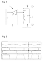
- the circuit diagram of Figure 1 illustrates an electronic circuit 1 comprising a circuit 3 representing a crystal oscillator and a prior art drive circuit 5 for driving the crystal oscillator 3.
- the crystal oscillator is modelled by a first capacitor C 1 , a second capacitor C 2 , an oscillator inductor L O , a resistor R O , a third capacitor C 3 and a fourth capacitor C 4 connected in parallel with the second capacitor, the coil and the resistor.
- One of the electrodes of the first and third capacitors is connected to ground.
- the drive circuit is modelled by an inverter circuit 7. This kind of drive circuit is currently widely used to drive crystal oscillators, for example.
- the inverter circuit 7 may comprise at least an n-type metal-oxide-semiconductor (MOS) transistor and a p-type MOS transistor, for example.
- MOS metal-oxide-semiconductor
- the crystal oscillator and the drive circuit are connected so as to form a positive feedback circuit, which induces an oscillation.
- the signal diagram of Figure 2 illustrates the behaviour of the signals of the electronic circuit 1 of Figure 1 . It is to be noted that, to better illustrate the results, the resistor R O has been omitted.
- the first (top) graph illustrates the voltage of the second capacitor C 2 as a function of time. In other words this graph illustrates the oscillation of the crystal oscillator.
- the second graph illustrates the output current of the drive circuit over time, while the third graph shows the drive circuit output voltage.
- the drive circuit 5 of Figure 1 drives the crystal oscillator 3 for a full half-cycle of the oscillation.
- the electronic circuit illustrated in Figure 1 is not optimal in terms of power consumption. More specifically, the current flow from the driver 5 is not in phase with the current flow of the crystal oscillator 3, and this causes power dissipation in the transistors of the driver 5. A further problem may arise due to the brief but significant current which may flow in the inverter 7 during each switching transition of the inverter 7. Such a transition current spike may arise if the inverter comprises an NMOS-PMOS transistor pair as mentioned above, where this pair effectively presents a short-circuit when both are momentarily on.
- the proposed new solution has the advantage that the operation of the drive circuit is more energy efficient than the state of the art drive circuits for oscillators. This is achieved by avoiding short circuit current and by driving the oscillator in phase with the oscillations of the oscillator, as explained later more in detail.
- an electronic circuit comprising the drive circuit and an oscillator driven by the drive circuit.
- a method of driving the oscillator According to a third aspect of the invention, there is provided a method of driving the oscillator.
- FIG 3 illustrates an electronic circuit 9 comprising a crystal oscillator 3, or more precisely a circuit representing the crystal oscillator 3, as in Figure 1 .
- the drive circuit 11 differs from the drive circuit 5 of Figure 1 .
- the drive circuit 11 comprises an electrical energy source 13, in this example a constant voltage source 13, connected between ground and a first terminal of a drive inductor L D , also referred to as a first inductor.
- a second terminal of the drive inductor is connected to a switching circuit, which is also connected to the crystal oscillator 3 as shown in Figure 3 .
- the switching circuit in this example comprises a first switch 17 and a second switch 19.
- the first switch is an NMOS transistor 17, while the second switch is a PMOS transistor 19.
- the drain terminal of the NMOS transistor 17 is connected to the second terminal of the drive inductor L D , while the source terminal of the NMOS transistor 17 is connected to ground.
- the gate of the NMOS transistor is connected to the crystal oscillator 3, and more particularly to a first node 21 located between the oscillator inductor L O , also referred to as a second inductor, and the second capacitor C 2 .
- the source of the PMOS transistor is connected to the second terminal of the drive inductor L D while the drain of the PMOS transistor 19 is connected to the crystal oscillator 3 and more specifically to a second node 23 located between the oscillator inductor L O and the third capacitor C 3 .
- the gate of the PMOS transistor is connected to the first node 21.
- the NMOS transistor 17 is on (i.e. the channel from drain to source is conductive), when its gate-source voltage is positive, and more specifically with its gate voltage above a first threshold value, such as 0.5 V from the ground.
- the PMOS transistor 19 on the other hand is on (i.e. the channel from source to drain is conductive) when its source-gate voltage is close to or greater than a second threshold of about 0.6 V. In this particular case, the second threshold value is greater than the first threshold value. This means that during a short time period the NMOS and PMOS transistors may both be conductive.
- the gate voltages of the NMOS and PMOS transistors 17, 19 start to rise.
- the PMOS transistor 19 turns off as the NMOS transistor 17 turns on, with the result that the current no longer flows to the crystal oscillator 3, but flows instead through the conductive drain-source channel of the NMOS transistor 17 to ground.
- the switching circuit is in an off state.
- the NMOS transistor 17 is on, the current flowing through the drive inductor L D stores energy temporarily in a magnetic field, for example in its coil. The drive inductor L D is therefore in a charging or energising state.
- the crystal oscillator has thus now started to oscillate, thanks to the energy provided to it at the beginning.
- the energy stored in the magnetic field "pushes" current from the voltage source 13 to the crystal oscillator 3.
- the drive inductor L D is therefore in a discharging or de-energising state.
- the PMOS transistor 19 then turns off again, as the NMOS transistor 17 turns on. The operation explained above will then be repeated according to a given sequence while the crystal oscillator 3 continues to oscillate.
- the signal diagram of Figure 4 illustrates the behaviour of the signals in the electronic circuit of Figure 3 .
- the two vertical lines in the diagram of Figure 4 show the duration of a full signal cycle.
- the first (top) graph shows the variation of the current through the drive inductor L D .
- the second graph from the top illustrates the variation of the crystal oscillator voltage, i.e. the electrical potential at the first node 21.
- the electrical potential measured at this node substantially corresponds also to the electrical potential at the gates of the first and second transistors 17, 19.
- the third graph from the top shows the current flow in the crystal oscillator 3, i.e. the magnitude of the current flowing through the oscillator inductor L O .
- the last graph illustrates the voltage of the crystal oscillator, i.e. the voltage across the third capacitor C 3 .
- the numerical values in Figure 4 are merely exemplary and ignore the resistance in the crystal oscillator 3.
- the voltage maintained by the constant voltage source 13 is about 3 V in this example.
- the operation of the NMOS and PMOS transistors can be approximated by stating that the NMOS transistor 17 is on and the PMOS transistor 19 is off during a positive half-cycle of the crystal oscillator voltage (second graph from the top in Figure 4 ); whereas the NMOS transistor 17 is off and the PMOS transistor 19 is on during a negative half-cycle of the crystal oscillator voltage.
- the present invention energy is temporarily stored in the drive inductor L D .
- the short circuit current which occurs in the prior art drive circuits can be avoided, because the energy is stored in the drive inductor L D instead of being shorted to ground.
- the electrical energy from the voltage source 13 is injected to the crystal oscillator 3 synchronously (i.e. in phase) with the oscillations of the crystal oscillator, with the help of the energy stored in the drive inductor L D . This means that the electrical energy is provided to the crystal oscillator 3 only at given time instants, and more particularly when the electrical potential at the first node 21 is below the second threshold value.
- the crystal oscillator 3 is fed with the current from the drive circuit 11 only when the crystal oscillator is ready to receive this current.
- the drive circuit 11 is in phase with the crystal oscillator 3 and the crystal oscillator 3 is not driven against the current flow of the crystal oscillator 3.
- the feed inductance, together with the oscillation frequency and the voltage of the constant voltage source 13 determine the amount of energy delivered to the oscillator 3 on each cycle.
- the value of the feed inductance may need to be tuned to the frequency, or to the particular oscillator.
- the present invention also relates to a method of driving the crystal oscillator 3 by supplying electrical energy from an electrical energy source 13 to the oscillator 3 via the drive inductor L D such that the drive inductor L D is energised by the electrical energy source 13 during a first phase of the oscillator cycle, during which the oscillator 3 is in a non-receptive state, and such that at least some of the energy stored in the drive inductor L D during the first phase is used to transfer electrical energy from the electrical energy source 13 to the oscillator 3 during a second phase of the oscillator cycle, during which the oscillator is in an energy-receptive state.
- the number of terminals of the transistors can be more than three.
- the number of terminals in some variants is four.
- the drive circuit can comprise further circuit elements, such as a capacitor pre-charging circuit for charging the capacitors of the oscillator, a current limiter for limiting the currents in the electronic circuit 11 and/or a control circuit for controlling the switching of the switches 17, 19 of the drive circuit 11 for example.
- a capacitor pre-charging circuit for charging the capacitors of the oscillator
- a current limiter for limiting the currents in the electronic circuit 11
- a control circuit for controlling the switching of the switches 17, 19 of the drive circuit 11 for example.
Landscapes
- Physics & Mathematics (AREA)
- Acoustics & Sound (AREA)
- General Physics & Mathematics (AREA)
- Oscillators With Electromechanical Resonators (AREA)
Abstract
Description
- The invention relates to the field of drive circuits for driving an oscillator circuit, such as a crystal oscillator used in watches, for example. The invention also relates to an electronic circuit comprising the drive circuit and the oscillator and to a method for driving the oscillator.
- The circuit diagram of
Figure 1 illustrates anelectronic circuit 1 comprising a circuit 3 representing a crystal oscillator and a prior art drive circuit 5 for driving the crystal oscillator 3. As can be seen, the crystal oscillator is modelled by a first capacitor C1, a second capacitor C2, an oscillator inductor LO, a resistor RO, a third capacitor C3 and a fourth capacitor C4 connected in parallel with the second capacitor, the coil and the resistor. One of the electrodes of the first and third capacitors is connected to ground. In the circuit ofFigure 1 , the drive circuit is modelled by aninverter circuit 7. This kind of drive circuit is currently widely used to drive crystal oscillators, for example. Theinverter circuit 7 may comprise at least an n-type metal-oxide-semiconductor (MOS) transistor and a p-type MOS transistor, for example. The crystal oscillator and the drive circuit are connected so as to form a positive feedback circuit, which induces an oscillation. - The signal diagram of
Figure 2 illustrates the behaviour of the signals of theelectronic circuit 1 ofFigure 1 . It is to be noted that, to better illustrate the results, the resistor RO has been omitted. The first (top) graph illustrates the voltage of the second capacitor C2 as a function of time. In other words this graph illustrates the oscillation of the crystal oscillator. The second graph illustrates the output current of the drive circuit over time, while the third graph shows the drive circuit output voltage. The drive circuit 5 ofFigure 1 drives the crystal oscillator 3 for a full half-cycle of the oscillation. In the second graph inFigure 2 , it can be seen that the current from the drive circuit flows in both directions during a semi-period of oscillation, which means that the energy in the oscillator inductor LO of the crystal oscillator 3 is not increased and the voltage across the crystal oscillator does not increase. Assuming ideal conditions, i.e. no resistance and every component ideal, then the current provided by the drive circuit 5 must be dissipated in the drive circuit 5. In a real application this means that the energy is dissipated in the parasitic resistance of the transistors of the drive circuit 5. - Thus it becomes clear that the electronic circuit illustrated in
Figure 1 is not optimal in terms of power consumption. More specifically, the current flow from the driver 5 is not in phase with the current flow of the crystal oscillator 3, and this causes power dissipation in the transistors of the driver 5. A further problem may arise due to the brief but significant current which may flow in theinverter 7 during each switching transition of theinverter 7. Such a transition current spike may arise if the inverter comprises an NMOS-PMOS transistor pair as mentioned above, where this pair effectively presents a short-circuit when both are momentarily on. - It is an object of the present invention to overcome the problems identified above related to oscillator drive circuits.
- According to a first aspect of the invention, there is provided a drive circuit for driving an oscillator as recited in
claim 1. - The proposed new solution has the advantage that the operation of the drive circuit is more energy efficient than the state of the art drive circuits for oscillators. This is achieved by avoiding short circuit current and by driving the oscillator in phase with the oscillations of the oscillator, as explained later more in detail.
- According to a second aspect of the invention, there is provided an electronic circuit comprising the drive circuit and an oscillator driven by the drive circuit.
- According to a third aspect of the invention, there is provided a method of driving the oscillator.
- Other aspects of the invention are recited in the dependent claims attached hereto.
- Other features and advantages of the invention will become apparent from the following description of a non-limiting exemplary embodiment, with reference to the appended drawings, in which :
-
Figure 1 is a circuit diagram illustrating a state of the art electronic circuit comprising a crystal oscillator and a drive circuit for driving the crystal oscillator; -
Figure 2 is a signal diagram illustrating the behaviour of the signals in the electronic circuit ofFigure 1 ; -
Figure 3 is a circuit diagram illustrating an electronic circuit comprising a crystal oscillator and a drive circuit according to an embodiment of the present invention for driving the crystal oscillator; and -
Figure 4 is a signal diagram illustrating the behaviour of the signals in the electronic circuit ofFigure 3 . - An embodiment of the present invention will now be described in detail with reference to the attached figures. The invention will be described in the context of a drive circuit for driving a crystal oscillator also known as a quartz of a watch. However, the disclosed drive circuit is not limited to be used in the context of crystal oscillators. Identical or corresponding functional and structural elements which appear in different drawings are assigned to the same reference numerals.
-
Figure 3 illustrates anelectronic circuit 9 comprising a crystal oscillator 3, or more precisely a circuit representing the crystal oscillator 3, as inFigure 1 . However, in the crystal oscillator ofFigure 3 , the resistor RO has been omitted. As can be seen, thedrive circuit 11 according to this embodiment differs from the drive circuit 5 ofFigure 1 . Thedrive circuit 11 comprises anelectrical energy source 13, in this example aconstant voltage source 13, connected between ground and a first terminal of a drive inductor LD, also referred to as a first inductor. A second terminal of the drive inductor is connected to a switching circuit, which is also connected to the crystal oscillator 3 as shown inFigure 3 . The switching circuit in this example comprises afirst switch 17 and asecond switch 19. In this illustrated example, the first switch is anNMOS transistor 17, while the second switch is aPMOS transistor 19. - As can be seen in
Figure 3 , the drain terminal of theNMOS transistor 17 is connected to the second terminal of the drive inductor LD, while the source terminal of theNMOS transistor 17 is connected to ground. The gate of the NMOS transistor is connected to the crystal oscillator 3, and more particularly to afirst node 21 located between the oscillator inductor LO, also referred to as a second inductor, and the second capacitor C2. The source of the PMOS transistor is connected to the second terminal of the drive inductor LD while the drain of thePMOS transistor 19 is connected to the crystal oscillator 3 and more specifically to asecond node 23 located between the oscillator inductor LO and the third capacitor C3. The gate of the PMOS transistor is connected to thefirst node 21. - In the present description, the
NMOS transistor 17 is on (i.e. the channel from drain to source is conductive), when its gate-source voltage is positive, and more specifically with its gate voltage above a first threshold value, such as 0.5 V from the ground. In the present description, thePMOS transistor 19 on the other hand is on (i.e. the channel from source to drain is conductive) when its source-gate voltage is close to or greater than a second threshold of about 0.6 V. In this particular case, the second threshold value is greater than the first threshold value. This means that during a short time period the NMOS and PMOS transistors may both be conductive. - Next, the operation of the
electronic circuit 9 is explained in more detail. In an initial state, when no electrical energy is supplied to the crystal oscillator 3, the capacitors of the crystal oscillator 3 are discharged and no current flows in the crystal oscillator. At this stage the gate voltages of the NMOS andPMOS transistors voltage source 13 is turned on, current starts to flow through the drive inductor LD and through the conductive source-drain channel of thePMOS transistor 19 to the crystal oscillator 3. At this point, current starts to flow in the crystal oscillator 3, and the capacitors C1, C2, C3, C4 start to charge. At the same time, the gate voltages of the NMOS andPMOS transistors PMOS transistor 19 turns off as theNMOS transistor 17 turns on, with the result that the current no longer flows to the crystal oscillator 3, but flows instead through the conductive drain-source channel of theNMOS transistor 17 to ground. In this state, the switching circuit is in an off state. When theNMOS transistor 17 is on, the current flowing through the drive inductor LD stores energy temporarily in a magnetic field, for example in its coil. The drive inductor LD is therefore in a charging or energising state. - The crystal oscillator has thus now started to oscillate, thanks to the energy provided to it at the beginning. This means that
NMOS transistor 17 turns off again, while thePMOS transistor 19 turns on, and the magnetic field energy is delivered as additional current flowing through thePMOS transistor 19 to thesecond node 23 in the crystal oscillator 3 to charge the capacitors in the crystal oscillator. In other words, at this point, the energy stored in the magnetic field "pushes" current from thevoltage source 13 to the crystal oscillator 3. Now, the drive inductor LD is therefore in a discharging or de-energising state. ThePMOS transistor 19 then turns off again, as theNMOS transistor 17 turns on. The operation explained above will then be repeated according to a given sequence while the crystal oscillator 3 continues to oscillate. - The signal diagram of
Figure 4 illustrates the behaviour of the signals in the electronic circuit ofFigure 3 . The two vertical lines in the diagram ofFigure 4 show the duration of a full signal cycle. The first (top) graph shows the variation of the current through the drive inductor LD. The second graph from the top illustrates the variation of the crystal oscillator voltage, i.e. the electrical potential at thefirst node 21. The electrical potential measured at this node substantially corresponds also to the electrical potential at the gates of the first andsecond transistors Figure 4 are merely exemplary and ignore the resistance in the crystal oscillator 3. The voltage maintained by theconstant voltage source 13 is about 3 V in this example. - In view of the explanation above, the operation of the NMOS and PMOS transistors can be approximated by stating that the
NMOS transistor 17 is on and thePMOS transistor 19 is off during a positive half-cycle of the crystal oscillator voltage (second graph from the top inFigure 4 ); whereas theNMOS transistor 17 is off and thePMOS transistor 19 is on during a negative half-cycle of the crystal oscillator voltage. Thus, during a positive half-cycle of the crystal oscillator voltage, the magnetic field energy increases, and when the crystal oscillator voltage becomes negative (second graph inFigure 4 ), the charge is pushed by the magnetic field of the drive inductor LD into the third capacitor C3 (last graph inFigure 4 ), thereby helping the oscillator inductor LO to increase its voltage again (second graph inFigure 4 ). - As has been explained above, according to the present invention energy is temporarily stored in the drive inductor LD. In this way, the short circuit current which occurs in the prior art drive circuits can be avoided, because the energy is stored in the drive inductor LD instead of being shorted to ground. Furthermore, the electrical energy from the
voltage source 13 is injected to the crystal oscillator 3 synchronously (i.e. in phase) with the oscillations of the crystal oscillator, with the help of the energy stored in the drive inductor LD. This means that the electrical energy is provided to the crystal oscillator 3 only at given time instants, and more particularly when the electrical potential at thefirst node 21 is below the second threshold value. Thus, according to the present invention, the crystal oscillator 3 is fed with the current from thedrive circuit 11 only when the crystal oscillator is ready to receive this current. In other words, according to the present invention thedrive circuit 11 is in phase with the crystal oscillator 3 and the crystal oscillator 3 is not driven against the current flow of the crystal oscillator 3. It is to be noted that the feed inductance, together with the oscillation frequency and the voltage of theconstant voltage source 13 determine the amount of energy delivered to the oscillator 3 on each cycle. Thus, the value of the feed inductance may need to be tuned to the frequency, or to the particular oscillator. - The present invention also relates to a method of driving the crystal oscillator 3 by supplying electrical energy from an
electrical energy source 13 to the oscillator 3 via the drive inductor LD such that the drive inductor LD is energised by theelectrical energy source 13 during a first phase of the oscillator cycle, during which the oscillator 3 is in a non-receptive state, and such that at least some of the energy stored in the drive inductor LD during the first phase is used to transfer electrical energy from theelectrical energy source 13 to the oscillator 3 during a second phase of the oscillator cycle, during which the oscillator is in an energy-receptive state. - While the invention has been illustrated and described in detail in the drawings and foregoing description, such illustration and description are to be considered illustrative or exemplary and not restrictive, the invention being not limited to the disclosed embodiment. Other embodiments and variants are understood, and can be achieved by those skilled in the art when carrying out the claimed invention, based on a study of the drawings, the disclosure and the appended claims. For instance, the number of terminals of the transistors can be more than three. The number of terminals in some variants is four. Moreover, the drive circuit can comprise further circuit elements, such as a capacitor pre-charging circuit for charging the capacitors of the oscillator, a current limiter for limiting the currents in the
electronic circuit 11 and/or a control circuit for controlling the switching of theswitches drive circuit 11 for example. - In the claims, the word "comprising" does not exclude other elements or steps, and the indefinite article "a" or "an" does not exclude a plurality. The mere fact that different features are recited in mutually different dependent claims does not indicate that a combination of these features cannot be advantageously used. Any reference signs in the claims should not be construed as limiting the scope of the invention.
Claims (16)
- Drive circuit (11) for driving an oscillator (3), the drive circuit (11) comprising:- a first inductor (LD) comprising a first terminal and a second terminal;- an electrical energy source (13) connected to the first terminal; and- a switching circuit connected between the second terminal and the oscillator (3), the switching circuit being configured to operate at least in an off state, in which it conveys substantially no electrical energy to the oscillator (3), and in an on state, in which it conveys electrical energy to the oscillator (3),characterized in that the first inductor (LD) is arranged to store energy in its magnetic field while the switching circuit is in the off state, and, when the switching circuit is in the on state, the switching circuit is arranged to use at least some of the energy stored in the magnetic field to deliver a surge of current from the electrical energy source (13) to the oscillator (3).
- Drive circuit (11) according to claim 1, characterized in that the switching circuit comprises a first switch (17) and a second switch (19).
- Drive circuit (11) according to claim 2, characterized in that the first switch comprises a first field-effect transistor (17), while the second switch comprises a second field-effect transistor (19).
- Drive circuit (11) according to any one of the preceding claims, characterized in that gate terminals of the first and second MOS transistors (17, 19) are connected to a common node (21), a drain of the first NMOS transistor (17) and a source of the second PMOS transistor (19) being connected to the second terminal of the first inductor (LD), and wherein the switching circuit is configured to be in the off state when the electrical potential at the common node (21) is greater than a first threshold value, and in the on state when an electrical difference potential between the second terminal and the common node (21) is above a second threshold value.
- Drive circuit (11) according to claim 4, characterized in that the second threshold value is higher than the first threshold value.
- Drive circuit (11) according to claim 4 or 5, characterized in that the first and second threshold values are positive voltages.
- Drive circuit (11) according to any one of claims 4 to 6, characterized in that the first and second threshold values are between 0 V and 1 V.
- Drive circuit (11) according to any one of claims 3 to 7, characterized in that the first transistor (17) comprises a NMOS transistor, while the second transistor comprises a PMOS transistor (19).
- Drive circuit (11) according to any one of claims 3 to 8, characterized in that a source terminal of the first transistor (17) is connected to ground, while a drain terminal of the first transistor (17) is connected to the second terminal.
- Drive circuit (11) according to any one of claims 3 to 8, characterized in that a source terminal of the second transistor (19) is connected to the second terminal.
- Drive circuit (11) according to any one of the preceding claims, characterized in that the electrical energy source (13) comprises a constant voltage source.
- Electronic circuit (9) comprising the drive circuit (11) according to any one of the preceding claims and the oscillator (3).
- Electronic circuit (9) according to claim 12, characterized in that the oscillator (3) comprises a second inductor (LO) comprising a third terminal (23) and a fourth terminal (21), and a capacitor (C2) connected in series with the second inductor (LO), and in that a drain terminal of the second transistor (19) is connected to the third terminal (23).
- Electronic circuit (9) according to claim 13 when dependent on claim 3, characterized in that gate terminals of the first and second transistors (17, 19) are connected to the fourth terminal (21).
- Electronic circuit (9) according to any one of claims 12 to 14, characterized in that the operation of the switching circuit is configured to be controlled by the electrical potential at the fourth terminal (21).
- Method of driving an oscillator (3) by supplying electrical energy from an electrical energy source (13) to the oscillator (3) via an inductor (LD) such that the inductor (LD) is energised by the electrical energy source (13) during a first phase of the oscillator cycle, during which the oscillator (3) is in a non-receptive state, and such that at least some of the energy stored in the inductor (LD) during the first phase is used to deliver a surge of current from the electrical energy source (13) to the oscillator (3) during a second phase of the oscillator cycle, during which the oscillator is in an energy-receptive state.
Priority Applications (5)
| Application Number | Priority Date | Filing Date | Title |
|---|---|---|---|
| EP15189081.1A EP3154191B1 (en) | 2015-10-09 | 2015-10-09 | Drive circuit for an oscillator |
| US15/270,652 US10003301B2 (en) | 2015-10-09 | 2016-09-20 | Drive circuit for an oscillator |
| JP2016188081A JP6393720B2 (en) | 2015-10-09 | 2016-09-27 | Driving circuit for an oscillator |
| KR1020160128397A KR101876065B1 (en) | 2015-10-09 | 2016-10-05 | Drive circuit for an oscillator |
| CN201610879531.1A CN106571789B (en) | 2015-10-09 | 2016-10-08 | For the method for driving oscillator, exciting circuit and its electronic circuit |
Applications Claiming Priority (1)
| Application Number | Priority Date | Filing Date | Title |
|---|---|---|---|
| EP15189081.1A EP3154191B1 (en) | 2015-10-09 | 2015-10-09 | Drive circuit for an oscillator |
Publications (2)
| Publication Number | Publication Date |
|---|---|
| EP3154191A1 true EP3154191A1 (en) | 2017-04-12 |
| EP3154191B1 EP3154191B1 (en) | 2020-12-30 |
Family
ID=54292673
Family Applications (1)
| Application Number | Title | Priority Date | Filing Date |
|---|---|---|---|
| EP15189081.1A Active EP3154191B1 (en) | 2015-10-09 | 2015-10-09 | Drive circuit for an oscillator |
Country Status (5)
| Country | Link |
|---|---|
| US (1) | US10003301B2 (en) |
| EP (1) | EP3154191B1 (en) |
| JP (1) | JP6393720B2 (en) |
| KR (1) | KR101876065B1 (en) |
| CN (1) | CN106571789B (en) |
Families Citing this family (2)
| Publication number | Priority date | Publication date | Assignee | Title |
|---|---|---|---|---|
| EP3663871A1 (en) * | 2018-12-06 | 2020-06-10 | The Swatch Group Research and Development Ltd | Motor drive unit of a dc electric motor |
| CN111628752B (en) * | 2020-06-02 | 2022-03-22 | 华南理工大学 | RC oscillator adopting pre-charging technology |
Citations (7)
| Publication number | Priority date | Publication date | Assignee | Title |
|---|---|---|---|---|
| WO1996030996A1 (en) * | 1995-03-24 | 1996-10-03 | Instituut Voor Milieu- En Agritechniek (Imag-Dlo) | Circuit for modulating a crystal oscillator with voltage-controlled (pin) diode |
| EP1184966A1 (en) * | 2000-08-24 | 2002-03-06 | Commissariat A L'energie Atomique | High-voltage pulse generator and electrical power supply equipped with such a generator |
| EP1753136A1 (en) * | 2004-05-31 | 2007-02-14 | Anritsu Corporation | Radar oscillator capable of preventing leakage of oscillation output |
| US20100188057A1 (en) * | 2006-08-05 | 2010-07-29 | Min Ming Tarng | Zilinx : the 11Less Green Technology for FPIC of Smart Window |
| US20100321124A1 (en) * | 2009-06-17 | 2010-12-23 | Qualcomm Incorporated | Configurable wide tuning range oscillator core |
| US20120267359A1 (en) * | 2011-04-22 | 2012-10-25 | Continental Automotive Systems Us, Inc. | Synchronous full-bridge oscillator |
| US20130135057A1 (en) * | 2011-11-25 | 2013-05-30 | Intel Mobile Communications GmbH | Common Mode Rejection Circuit |
Family Cites Families (9)
| Publication number | Priority date | Publication date | Assignee | Title |
|---|---|---|---|---|
| US5517158A (en) * | 1994-12-13 | 1996-05-14 | At&T Corp. | Self-timed oscillator circuit including starting and stopping circuitry |
| US20040263272A1 (en) * | 2003-06-30 | 2004-12-30 | Ashoke Ravi | Enhanced single-supply low-voltage circuits and methods thereof |
| JP2006157767A (en) * | 2004-12-01 | 2006-06-15 | Renesas Technology Corp | Communication semiconductor integrated circuit with built-in oscillation circuit, communication system, and manufacturing method of semiconductor integrated circuit |
| US7479838B1 (en) * | 2005-05-25 | 2009-01-20 | Athas William C | Energy efficient waveform generation using tuned resonators |
| JP4597044B2 (en) * | 2005-12-09 | 2010-12-15 | 株式会社リコー | Backflow prevention circuit |
| KR101443583B1 (en) * | 2008-04-29 | 2014-11-03 | 세미컨덕터 콤포넨츠 인더스트리즈 엘엘씨 | Method for regulating an output voltage |
| JP2010087571A (en) * | 2008-09-29 | 2010-04-15 | Nec Electronics Corp | Oscillation circuit and method of controlling the same |
| JP5465891B2 (en) * | 2009-02-18 | 2014-04-09 | 日本電波工業株式会社 | Crystal oscillation circuit |
| CN103178835B (en) * | 2013-03-08 | 2015-08-12 | 无锡泽太微电子有限公司 | Crystal oscillator and the method that crystal oscillator acceleration is vibrated |
-
2015
- 2015-10-09 EP EP15189081.1A patent/EP3154191B1/en active Active
-
2016
- 2016-09-20 US US15/270,652 patent/US10003301B2/en active Active
- 2016-09-27 JP JP2016188081A patent/JP6393720B2/en active Active
- 2016-10-05 KR KR1020160128397A patent/KR101876065B1/en active IP Right Grant
- 2016-10-08 CN CN201610879531.1A patent/CN106571789B/en active Active
Patent Citations (7)
| Publication number | Priority date | Publication date | Assignee | Title |
|---|---|---|---|---|
| WO1996030996A1 (en) * | 1995-03-24 | 1996-10-03 | Instituut Voor Milieu- En Agritechniek (Imag-Dlo) | Circuit for modulating a crystal oscillator with voltage-controlled (pin) diode |
| EP1184966A1 (en) * | 2000-08-24 | 2002-03-06 | Commissariat A L'energie Atomique | High-voltage pulse generator and electrical power supply equipped with such a generator |
| EP1753136A1 (en) * | 2004-05-31 | 2007-02-14 | Anritsu Corporation | Radar oscillator capable of preventing leakage of oscillation output |
| US20100188057A1 (en) * | 2006-08-05 | 2010-07-29 | Min Ming Tarng | Zilinx : the 11Less Green Technology for FPIC of Smart Window |
| US20100321124A1 (en) * | 2009-06-17 | 2010-12-23 | Qualcomm Incorporated | Configurable wide tuning range oscillator core |
| US20120267359A1 (en) * | 2011-04-22 | 2012-10-25 | Continental Automotive Systems Us, Inc. | Synchronous full-bridge oscillator |
| US20130135057A1 (en) * | 2011-11-25 | 2013-05-30 | Intel Mobile Communications GmbH | Common Mode Rejection Circuit |
Also Published As
| Publication number | Publication date |
|---|---|
| US10003301B2 (en) | 2018-06-19 |
| CN106571789B (en) | 2019-04-23 |
| KR101876065B1 (en) | 2018-08-02 |
| JP2017073768A (en) | 2017-04-13 |
| EP3154191B1 (en) | 2020-12-30 |
| JP6393720B2 (en) | 2018-09-19 |
| CN106571789A (en) | 2017-04-19 |
| KR20170042479A (en) | 2017-04-19 |
| US20170104454A1 (en) | 2017-04-13 |
Similar Documents
| Publication | Publication Date | Title |
|---|---|---|
| US8513937B2 (en) | Switching regulator with optimized switch node rise time | |
| US8928363B2 (en) | Semiconductor drive circuit and power conversion apparatus using same | |
| US7459945B2 (en) | Gate driving circuit and gate driving method of power MOSFET | |
| JP4286541B2 (en) | Switching type FET circuit | |
| US20220224330A1 (en) | Driving D-Mode and E-Mode FETS in Half-Bridge Driver Configuration | |
| EP1521366A2 (en) | Method and apparatus for simplifying the control of a switch | |
| EP3282491B1 (en) | Led drive circuit | |
| JP6859668B2 (en) | Load drive circuit | |
| US10305412B2 (en) | Semiconductor device | |
| US9912332B2 (en) | Semiconductor device | |
| JP2007174134A (en) | High-speed gate drive circuit | |
| JP2008182381A (en) | High-speed gate drive circuit | |
| US7719245B2 (en) | Methods and apparatus to provide self-tracking pre-driver controls | |
| US10476383B2 (en) | Negative charge pump circuit | |
| US20210184667A1 (en) | Semiconductor integrated circuit and control method of semiconductor integrated circuit | |
| US8390337B2 (en) | Electronic device and method for DC-DC conversion | |
| US10003301B2 (en) | Drive circuit for an oscillator | |
| US9270255B2 (en) | High voltage driver using low voltage transistor | |
| KR100527528B1 (en) | Motor driving device for supplying driving current to a three-phase motor through output transistors | |
| CN110265262B (en) | Driving circuit for inductive relay and rapid demagnetization method | |
| US10536145B2 (en) | High-speed MOSFET and IGBT gate driver | |
| KR20170076497A (en) | Drive circuit | |
| JP2009159696A (en) | Switching power supply device | |
| EP3513487A1 (en) | Dc-dc converters | |
| US9130451B2 (en) | Circuitry, multi-branch charge pump, method for controlling a charge pump and system |
Legal Events
| Date | Code | Title | Description |
|---|---|---|---|
| PUAI | Public reference made under article 153(3) epc to a published international application that has entered the european phase |
Free format text: ORIGINAL CODE: 0009012 |
|
| STAA | Information on the status of an ep patent application or granted ep patent |
Free format text: STATUS: THE APPLICATION HAS BEEN PUBLISHED |
|
| AK | Designated contracting states |
Kind code of ref document: A1 Designated state(s): AL AT BE BG CH CY CZ DE DK EE ES FI FR GB GR HR HU IE IS IT LI LT LU LV MC MK MT NL NO PL PT RO RS SE SI SK SM TR |
|
| AX | Request for extension of the european patent |
Extension state: BA ME |
|
| STAA | Information on the status of an ep patent application or granted ep patent |
Free format text: STATUS: REQUEST FOR EXAMINATION WAS MADE |
|
| 17P | Request for examination filed |
Effective date: 20171012 |
|
| RBV | Designated contracting states (corrected) |
Designated state(s): AL AT BE BG CH CY CZ DE DK EE ES FI FR GB GR HR HU IE IS IT LI LT LU LV MC MK MT NL NO PL PT RO RS SE SI SK SM TR |
|
| REG | Reference to a national code |
Ref country code: DE Ref legal event code: R079 Ref document number: 602015064055 Country of ref document: DE Free format text: PREVIOUS MAIN CLASS: H03B0005360000 Ipc: H03K0021380000 |
|
| RIC1 | Information provided on ipc code assigned before grant |
Ipc: H03B 5/36 20060101ALI20200825BHEP Ipc: H03K 21/38 20060101AFI20200825BHEP |
|
| GRAP | Despatch of communication of intention to grant a patent |
Free format text: ORIGINAL CODE: EPIDOSNIGR1 |
|
| STAA | Information on the status of an ep patent application or granted ep patent |
Free format text: STATUS: GRANT OF PATENT IS INTENDED |
|
| INTG | Intention to grant announced |
Effective date: 20201006 |
|
| GRAS | Grant fee paid |
Free format text: ORIGINAL CODE: EPIDOSNIGR3 |
|
| GRAA | (expected) grant |
Free format text: ORIGINAL CODE: 0009210 |
|
| STAA | Information on the status of an ep patent application or granted ep patent |
Free format text: STATUS: THE PATENT HAS BEEN GRANTED |
|
| AK | Designated contracting states |
Kind code of ref document: B1 Designated state(s): AL AT BE BG CH CY CZ DE DK EE ES FI FR GB GR HR HU IE IS IT LI LT LU LV MC MK MT NL NO PL PT RO RS SE SI SK SM TR |
|
| REG | Reference to a national code |
Ref country code: GB Ref legal event code: FG4D |
|
| REG | Reference to a national code |
Ref country code: AT Ref legal event code: REF Ref document number: 1350945 Country of ref document: AT Kind code of ref document: T Effective date: 20210115 Ref country code: CH Ref legal event code: NV Representative=s name: ICB INGENIEURS CONSEILS EN BREVETS SA, CH |
|
| REG | Reference to a national code |
Ref country code: DE Ref legal event code: R096 Ref document number: 602015064055 Country of ref document: DE |
|
| REG | Reference to a national code |
Ref country code: IE Ref legal event code: FG4D |
|
| PG25 | Lapsed in a contracting state [announced via postgrant information from national office to epo] |
Ref country code: FI Free format text: LAPSE BECAUSE OF FAILURE TO SUBMIT A TRANSLATION OF THE DESCRIPTION OR TO PAY THE FEE WITHIN THE PRESCRIBED TIME-LIMIT Effective date: 20201230 Ref country code: RS Free format text: LAPSE BECAUSE OF FAILURE TO SUBMIT A TRANSLATION OF THE DESCRIPTION OR TO PAY THE FEE WITHIN THE PRESCRIBED TIME-LIMIT Effective date: 20201230 Ref country code: NO Free format text: LAPSE BECAUSE OF FAILURE TO SUBMIT A TRANSLATION OF THE DESCRIPTION OR TO PAY THE FEE WITHIN THE PRESCRIBED TIME-LIMIT Effective date: 20210330 Ref country code: GR Free format text: LAPSE BECAUSE OF FAILURE TO SUBMIT A TRANSLATION OF THE DESCRIPTION OR TO PAY THE FEE WITHIN THE PRESCRIBED TIME-LIMIT Effective date: 20210331 |
|
| REG | Reference to a national code |
Ref country code: AT Ref legal event code: MK05 Ref document number: 1350945 Country of ref document: AT Kind code of ref document: T Effective date: 20201230 |
|
| PG25 | Lapsed in a contracting state [announced via postgrant information from national office to epo] |
Ref country code: SE Free format text: LAPSE BECAUSE OF FAILURE TO SUBMIT A TRANSLATION OF THE DESCRIPTION OR TO PAY THE FEE WITHIN THE PRESCRIBED TIME-LIMIT Effective date: 20201230 Ref country code: LV Free format text: LAPSE BECAUSE OF FAILURE TO SUBMIT A TRANSLATION OF THE DESCRIPTION OR TO PAY THE FEE WITHIN THE PRESCRIBED TIME-LIMIT Effective date: 20201230 Ref country code: BG Free format text: LAPSE BECAUSE OF FAILURE TO SUBMIT A TRANSLATION OF THE DESCRIPTION OR TO PAY THE FEE WITHIN THE PRESCRIBED TIME-LIMIT Effective date: 20210330 |
|
| REG | Reference to a national code |
Ref country code: NL Ref legal event code: MP Effective date: 20201230 |
|
| PG25 | Lapsed in a contracting state [announced via postgrant information from national office to epo] |
Ref country code: HR Free format text: LAPSE BECAUSE OF FAILURE TO SUBMIT A TRANSLATION OF THE DESCRIPTION OR TO PAY THE FEE WITHIN THE PRESCRIBED TIME-LIMIT Effective date: 20201230 |
|
| REG | Reference to a national code |
Ref country code: LT Ref legal event code: MG9D |
|
| PG25 | Lapsed in a contracting state [announced via postgrant information from national office to epo] |
Ref country code: PT Free format text: LAPSE BECAUSE OF FAILURE TO SUBMIT A TRANSLATION OF THE DESCRIPTION OR TO PAY THE FEE WITHIN THE PRESCRIBED TIME-LIMIT Effective date: 20210430 Ref country code: SK Free format text: LAPSE BECAUSE OF FAILURE TO SUBMIT A TRANSLATION OF THE DESCRIPTION OR TO PAY THE FEE WITHIN THE PRESCRIBED TIME-LIMIT Effective date: 20201230 Ref country code: RO Free format text: LAPSE BECAUSE OF FAILURE TO SUBMIT A TRANSLATION OF THE DESCRIPTION OR TO PAY THE FEE WITHIN THE PRESCRIBED TIME-LIMIT Effective date: 20201230 Ref country code: LT Free format text: LAPSE BECAUSE OF FAILURE TO SUBMIT A TRANSLATION OF THE DESCRIPTION OR TO PAY THE FEE WITHIN THE PRESCRIBED TIME-LIMIT Effective date: 20201230 Ref country code: EE Free format text: LAPSE BECAUSE OF FAILURE TO SUBMIT A TRANSLATION OF THE DESCRIPTION OR TO PAY THE FEE WITHIN THE PRESCRIBED TIME-LIMIT Effective date: 20201230 Ref country code: CZ Free format text: LAPSE BECAUSE OF FAILURE TO SUBMIT A TRANSLATION OF THE DESCRIPTION OR TO PAY THE FEE WITHIN THE PRESCRIBED TIME-LIMIT Effective date: 20201230 Ref country code: NL Free format text: LAPSE BECAUSE OF FAILURE TO SUBMIT A TRANSLATION OF THE DESCRIPTION OR TO PAY THE FEE WITHIN THE PRESCRIBED TIME-LIMIT Effective date: 20201230 |
|
| PG25 | Lapsed in a contracting state [announced via postgrant information from national office to epo] |
Ref country code: PL Free format text: LAPSE BECAUSE OF FAILURE TO SUBMIT A TRANSLATION OF THE DESCRIPTION OR TO PAY THE FEE WITHIN THE PRESCRIBED TIME-LIMIT Effective date: 20201230 Ref country code: AT Free format text: LAPSE BECAUSE OF FAILURE TO SUBMIT A TRANSLATION OF THE DESCRIPTION OR TO PAY THE FEE WITHIN THE PRESCRIBED TIME-LIMIT Effective date: 20201230 |
|
| PG25 | Lapsed in a contracting state [announced via postgrant information from national office to epo] |
Ref country code: IS Free format text: LAPSE BECAUSE OF FAILURE TO SUBMIT A TRANSLATION OF THE DESCRIPTION OR TO PAY THE FEE WITHIN THE PRESCRIBED TIME-LIMIT Effective date: 20210430 |
|
| REG | Reference to a national code |
Ref country code: DE Ref legal event code: R097 Ref document number: 602015064055 Country of ref document: DE |
|
| PG25 | Lapsed in a contracting state [announced via postgrant information from national office to epo] |
Ref country code: AL Free format text: LAPSE BECAUSE OF FAILURE TO SUBMIT A TRANSLATION OF THE DESCRIPTION OR TO PAY THE FEE WITHIN THE PRESCRIBED TIME-LIMIT Effective date: 20201230 Ref country code: IT Free format text: LAPSE BECAUSE OF FAILURE TO SUBMIT A TRANSLATION OF THE DESCRIPTION OR TO PAY THE FEE WITHIN THE PRESCRIBED TIME-LIMIT Effective date: 20201230 |
|
| PLBE | No opposition filed within time limit |
Free format text: ORIGINAL CODE: 0009261 |
|
| STAA | Information on the status of an ep patent application or granted ep patent |
Free format text: STATUS: NO OPPOSITION FILED WITHIN TIME LIMIT |
|
| PG25 | Lapsed in a contracting state [announced via postgrant information from national office to epo] |
Ref country code: ES Free format text: LAPSE BECAUSE OF FAILURE TO SUBMIT A TRANSLATION OF THE DESCRIPTION OR TO PAY THE FEE WITHIN THE PRESCRIBED TIME-LIMIT Effective date: 20201230 Ref country code: DK Free format text: LAPSE BECAUSE OF FAILURE TO SUBMIT A TRANSLATION OF THE DESCRIPTION OR TO PAY THE FEE WITHIN THE PRESCRIBED TIME-LIMIT Effective date: 20201230 |
|
| 26N | No opposition filed |
Effective date: 20211001 |
|
| PG25 | Lapsed in a contracting state [announced via postgrant information from national office to epo] |
Ref country code: SI Free format text: LAPSE BECAUSE OF FAILURE TO SUBMIT A TRANSLATION OF THE DESCRIPTION OR TO PAY THE FEE WITHIN THE PRESCRIBED TIME-LIMIT Effective date: 20201230 |
|
| PG25 | Lapsed in a contracting state [announced via postgrant information from national office to epo] |
Ref country code: IS Free format text: LAPSE BECAUSE OF FAILURE TO SUBMIT A TRANSLATION OF THE DESCRIPTION OR TO PAY THE FEE WITHIN THE PRESCRIBED TIME-LIMIT Effective date: 20210430 |
|
| REG | Reference to a national code |
Ref country code: BE Ref legal event code: MM Effective date: 20211031 |
|
| GBPC | Gb: european patent ceased through non-payment of renewal fee |
Effective date: 20211009 |
|
| PG25 | Lapsed in a contracting state [announced via postgrant information from national office to epo] |
Ref country code: MC Free format text: LAPSE BECAUSE OF FAILURE TO SUBMIT A TRANSLATION OF THE DESCRIPTION OR TO PAY THE FEE WITHIN THE PRESCRIBED TIME-LIMIT Effective date: 20201230 |
|
| PG25 | Lapsed in a contracting state [announced via postgrant information from national office to epo] |
Ref country code: LU Free format text: LAPSE BECAUSE OF NON-PAYMENT OF DUE FEES Effective date: 20211009 Ref country code: GB Free format text: LAPSE BECAUSE OF NON-PAYMENT OF DUE FEES Effective date: 20211009 Ref country code: BE Free format text: LAPSE BECAUSE OF NON-PAYMENT OF DUE FEES Effective date: 20211031 |
|
| PG25 | Lapsed in a contracting state [announced via postgrant information from national office to epo] |
Ref country code: IE Free format text: LAPSE BECAUSE OF NON-PAYMENT OF DUE FEES Effective date: 20211009 |
|
| PG25 | Lapsed in a contracting state [announced via postgrant information from national office to epo] |
Ref country code: HU Free format text: LAPSE BECAUSE OF FAILURE TO SUBMIT A TRANSLATION OF THE DESCRIPTION OR TO PAY THE FEE WITHIN THE PRESCRIBED TIME-LIMIT; INVALID AB INITIO Effective date: 20151009 |
|
| PG25 | Lapsed in a contracting state [announced via postgrant information from national office to epo] |
Ref country code: CY Free format text: LAPSE BECAUSE OF FAILURE TO SUBMIT A TRANSLATION OF THE DESCRIPTION OR TO PAY THE FEE WITHIN THE PRESCRIBED TIME-LIMIT Effective date: 20201230 |
|
| P01 | Opt-out of the competence of the unified patent court (upc) registered |
Effective date: 20230615 |
|
| PG25 | Lapsed in a contracting state [announced via postgrant information from national office to epo] |
Ref country code: SM Free format text: LAPSE BECAUSE OF FAILURE TO SUBMIT A TRANSLATION OF THE DESCRIPTION OR TO PAY THE FEE WITHIN THE PRESCRIBED TIME-LIMIT Effective date: 20201230 |
|
| PGFP | Annual fee paid to national office [announced via postgrant information from national office to epo] |
Ref country code: FR Payment date: 20230920 Year of fee payment: 9 |
|
| PGFP | Annual fee paid to national office [announced via postgrant information from national office to epo] |
Ref country code: DE Payment date: 20230920 Year of fee payment: 9 Ref country code: CH Payment date: 20231101 Year of fee payment: 9 |