EP3154149A1 - System and method for deep discharge protection of a battery - Google Patents
System and method for deep discharge protection of a battery Download PDFInfo
- Publication number
- EP3154149A1 EP3154149A1 EP15465549.2A EP15465549A EP3154149A1 EP 3154149 A1 EP3154149 A1 EP 3154149A1 EP 15465549 A EP15465549 A EP 15465549A EP 3154149 A1 EP3154149 A1 EP 3154149A1
- Authority
- EP
- European Patent Office
- Prior art keywords
- battery
- chargeable battery
- chargeable
- electronic device
- internal switch
- Prior art date
- Legal status (The legal status is an assumption and is not a legal conclusion. Google has not performed a legal analysis and makes no representation as to the accuracy of the status listed.)
- Granted
Links
Images


Classifications
-
- H—ELECTRICITY
- H02—GENERATION; CONVERSION OR DISTRIBUTION OF ELECTRIC POWER
- H02J—ELECTRIC POWER NETWORKS; CIRCUIT ARRANGEMENTS OR SYSTEMS FOR SUPPLYING OR DISTRIBUTING ELECTRIC POWER; SYSTEMS FOR STORING ELECTRIC ENERGY
- H02J7/00—Circuit arrangements for charging or discharging batteries or for supplying loads from batteries
- H02J7/60—Circuit arrangements for charging or discharging batteries or for supplying loads from batteries including safety or protection arrangements
- H02J7/663—Circuit arrangements for charging or discharging batteries or for supplying loads from batteries including safety or protection arrangements using battery or load disconnect circuits
-
- H—ELECTRICITY
- H02—GENERATION; CONVERSION OR DISTRIBUTION OF ELECTRIC POWER
- H02J—ELECTRIC POWER NETWORKS; CIRCUIT ARRANGEMENTS OR SYSTEMS FOR SUPPLYING OR DISTRIBUTING ELECTRIC POWER; SYSTEMS FOR STORING ELECTRIC ENERGY
- H02J7/00—Circuit arrangements for charging or discharging batteries or for supplying loads from batteries
- H02J7/02—Circuit arrangements for charging or discharging batteries or for supplying loads from batteries for charging batteries from AC mains by converters
- H02J7/04—Regulation of charging current or voltage
-
- H—ELECTRICITY
- H02—GENERATION; CONVERSION OR DISTRIBUTION OF ELECTRIC POWER
- H02J—ELECTRIC POWER NETWORKS; CIRCUIT ARRANGEMENTS OR SYSTEMS FOR SUPPLYING OR DISTRIBUTING ELECTRIC POWER; SYSTEMS FOR STORING ELECTRIC ENERGY
- H02J7/00—Circuit arrangements for charging or discharging batteries or for supplying loads from batteries
- H02J7/90—Regulation of charging or discharging current or voltage
- H02J7/96—Regulation of charging or discharging current or voltage in response to battery voltage
-
- H—ELECTRICITY
- H02—GENERATION; CONVERSION OR DISTRIBUTION OF ELECTRIC POWER
- H02J—ELECTRIC POWER NETWORKS; CIRCUIT ARRANGEMENTS OR SYSTEMS FOR SUPPLYING OR DISTRIBUTING ELECTRIC POWER; SYSTEMS FOR STORING ELECTRIC ENERGY
- H02J7/00—Circuit arrangements for charging or discharging batteries or for supplying loads from batteries
- H02J7/60—Circuit arrangements for charging or discharging batteries or for supplying loads from batteries including safety or protection arrangements
- H02J7/63—Circuit arrangements for charging or discharging batteries or for supplying loads from batteries including safety or protection arrangements against overdischarge
Definitions
- the current invention refers to a system and a method for deep discharge protection of a battery, particularly of a lithium-ion battery.
- Rechargeable lithium-ion (li-ion) batteries are used for many different applications, e.g. in consumer and automotive electronics.
- a li-ion battery may be used for powering a so-called on-board unit.
- toll roads also known as turnpikes or tollways
- Different systems for collecting the toll are known, for example electronic road toll systems.
- electronic road toll systems an on-board unit is installed in the vehicle to determine the position of the vehicle and transmit position data to a central office for billing.
- Such deep discharge protection circuits generally include a switch, mostly a transistor, which disconnects the battery from the system, when the battery voltage decreases below a certain level.
- MOS metal oxide semiconductor
- the problem to be solved by the current invention is, therefore, to provide a system and a method for deep discharge protection of a battery which overcomes the above disadvantages.
- a system for deep discharge protection of a chargeable battery in an electronic device comprises a chargeable battery, which is configured to provide energy to a system, when operation of the electronic device is needed and no other energy source is available.
- the system further comprises a battery charging unit with an internal switch, wherein the battery charging unit is coupled to the chargeable battery and is configured to charge the chargeable battery.
- the system further comprises a deep discharge protection unit and a transport mode unit.
- the discharge protection unit is configured to monitor a voltage of the chargeable battery and disconnect the chargeable battery from the system, when the battery voltage is lower than a given threshold voltage and the transport mode unit is configured to trigger an opening the internal switch of the battery charging unit, wherein the chargeable battery is disconnected from the system when the at least one switch is opened.
- the deep discharge protection unit may be configured to trigger an opening of the internal switch of the battery charging unit when the battery voltage is lower than the given threshold voltage. A deep discharge of the chargeable battery may therefore be prevented during the normal operation of the electronic device.
- an opening of the internal switch may be triggered after the first insertion of the chargeable battery in the electronic device at the end of the production line and before connecting the electronic device to an external energy source.
- a deep discharge during shipment of the device may be prevented.
- the electronic device may be mounted in a vehicle and the external energy source is a vehicle battery.
- the electronic device may be an on-board unit.
- the system may comprise a controller, which is configured to enable or disable a charging of the chargeable battery.
- the controller may be configured to receive a manual input, which indicates that a disconnection of the chargeable battery from the system is desired. For example, an operator may instruct the controller at the end of the production line to disconnect the chargeable battery from the system.
- the controller may be further configured to output a transport signal, when a manual input is received, wherein the transport signal triggers an opening of the internal switch of the battery charging unit.
- the internal switch may be closed and the chargeable battery coupled to the system again, when the electronic device is coupled to the external energy source. No further command is needed to return the system from the transport mode to a running mode. A customer may resume the functionalities of the system by simply plugging it to an energy source.
- the battery may be a lithium-ion or a nickel-cadmium battery. Such batteries may be charged. They have a very high energy density compared to other batteries. Further, lithium-ion batteries may be charged up to comparably high voltages.
- a method for deep discharge protection of a chargeable battery in an electronic device comprises charging the chargeable battery by means of a battery charging unit which is coupled to the chargeable battery and which comprises an internal switch.
- the method further comprises using the chargeable battery to provide energy to a system, when operation of the electronic device is needed and no other energy source than the chargeable battery is available, monitoring a voltage of the chargeable battery and disconnecting the chargeable battery from the system, when the battery voltage is lower than a given threshold voltage.
- An opening of the internal switch of the battery charging unit is triggered, wherein the chargeable battery is disconnected from the system when the at least one switch is opened.
- An opening of the internal switch of the battery charging unit may be triggered when the battery voltage is lower than the given threshold voltage.
- an opening of the internal switch may be triggered after the first insertion of the chargeable battery in the electronic device at the end of the production line and before connecting the electronic device to an external energy source.
- FIG. 1 illustrates in a block diagram a battery charging circuit.
- the battery charging circuit includes a chargeable battery 1, which may be a lithium-ion (li-ion) battery. With a first output, the chargeable battery 1 is coupled to a second terminal V2 for a second potential, which may be ground, for example.
- a battery charging unit 2 is coupled between a second output of the chargeable battery 1 and a first terminal V1 for a first potential.
- the first terminal V1 may be coupled to a vehicle battery, for example. More precisely, the first terminal V1 may be coupled to what is generally known as terminal 30.
- the battery charging circuit may be integrated in an electronic device such as an on-board unit, for example.
- An on-board unit usually is configured to determine the position of a vehicle in regular intervals and provide this position data to a central office for billing. Therefore, one or more devices (e.g. controllers), which perform the functionalities of the electronic device, are further included in the battery charging circuit. Such devices are represented as the system 3, which is coupled to the battery charging unit 2. The system 3 may be powered by the vehicle battery or, if the vehicle battery is not connected, by the chargeable battery 1.
- the battery charging unit 2 is configured to provide power to the system 3, as well as to charge the chargeable battery 1, if desired. It is possible that at one point, the battery charging unit 2 only provides power to the system 3, but battery charging is disabled (e.g. when the chargeable battery is fully charged). It is, however, also possible that the battery charging unit 2 provides power to the system 3 and at the same time charges the chargeable battery 1. Further, it is possible that the battery charging unit charges the chargeable battery 1, while no power is provided to the system 3.
- the system 3 may include a controller (not illustrated in Figure 1 ), which is configured to enable the battery charging unit 2 to charge the chargeable battery 1, if charging of the chargeable battery 1 is required.
- the controller may be further configured to disable the battery charging unit 2, if charging of the chargeable battery 1 is not required.
- a deep discharge protection unit 4 is included in the battery charging circuit of Figure 1 .
- the deep discharge protection unit 4 is configured to determine a voltage of the chargeable battery 1. Every chargeable battery 1 may be charged up to a maximum voltage, e.g. 4.2V. When the chargeable battery 1 powers a system 3, the battery voltage decreases.
- the deep discharge protection unit 4 is further configured to compare the determined battery voltage to a predetermined threshold voltage. If the battery voltage falls below the threshold voltage, the chargeable battery 1 is disconnected from the system 3 by means of a switch S1.
- the switch S1 may be a power MOS-transistor, for example. When disconnected from the system 3, no more energy is provided to the system 3 and any other components and deep discharge may be prevented.
- the battery charging circuit illustrated in Figure 1 especially the switch S1, which is coupled between the system 3 and the battery charging unit 2, has several drawbacks.
- the switch S1 which is usually implemented as a transistor, needs to be a rather big and, therefore, expensive switch (e.g. power transistor) in order to sufficiently protect the chargeable battery 1 from discharging.
- the switch S1 is omitted.
- a transport mode unit 5 is coupled between the deep discharge protection unit 4 and the first terminal V1.
- the transport mode unit 5 is configured to initiate a disconnection of the chargeable battery 1 from the other components, especially from the system 3.
- the charging unit 2 when disconnecting the chargeable battery 1 from the system 3, the charging unit 2 functions as a switching device. Therefore, the charging unit 2 includes at least one internal switch S2. By opening this at least one internal switch S2, the chargeable battery 1 may be disconnected from the rest of the battery charging system.
- a internal switch S2 which may be used to disconnect the chargeable battery 1.
- the chargeable battery 1, by means of that internal switch S2, may be disconnected from the system 3 during transportation from the manufacturer of the on-board unit until its installation in a vehicle.
- the internal switch S2, however, may also be used to disconnect the chargeable battery 1 from the system 3 after installation in a vehicle, when the battery voltage falls below a certain threshold.
- the chargeable battery 1 will be inserted in the on-board unit. Usually, at this point, the chargeable battery 1 is partly or completely charged.
- the chargeable battery 1 will provide at least a small amount of power to the other components of the on-board unit (the system 3). If the on-board unit is not connected to a vehicle battery after a certain time, the chargeable battery 1 may be completely discharged and, therefore, may be damaged. Therefore, after inserting the chargeable battery in the on-board unit, the system 3 may send a first transport signal TS to the transport mode unit 5.
- the transport mode unit 5 again sends a second signal X1 to the deep discharge protection unit 4. This results in a third signal DIS being sent to the charging unit 2.
- This third signal DIS causes the charging unit 2 to decouple the chargeable battery 1 from the system 3 by opening the internal switch S2.
- the on-board unit at this moment enters a transportation mode.
- the on-board unit When the on-board unit is mounted on a vehicle and the vehicle battery is connected to the on-board unit (terminal V1 of the battery charging system will be connected to the vehicle battery), the chargeable battery 1 will again be coupled to the system 3. By connecting the vehicle battery, the on-board unit will exit the transportation mode and resume its normal operation.
- FIG. 3 illustrates one example of a charging unit 2 in greater detail.
- the charging unit 2 includes a charging IC 21 (integrated circuit).
- Charging ICs are special devices, which are configured to enable or disable the charging of a chargeable battery 1.
- Charging ICs are offered by several different semiconductor companies. Each charging IC 21 usually requires an individual wiring of the different pins. Generally some kind of protection circuitry is needed or components such as resistors and capacitors have to be connected to certain pins, in order to enable certain functionalities of the charging IC 21. The particular wiring depends on the model of the charging IC. Therefore, the circuit illustrated in Figure 3 is only an example.
- the charging unit 2 may be implemented in any other suitable way. In the circuit illustrated in Figure 3 , pins and components, which are not needed for the current invention but might be included in a charging IC 21 are omitted.
- the charging IC 21 may be coupled to the second terminal V2, which may be ground, for example, with a first pin VSS.
- the charging IC 21 may receive a signal BAT_DIS.
- the second pin SYSOFF may be a system enable input, for example. If the signal BAT_DIS is provided to the second pin SYSOFF, the chargeable battery 1 is connected to the system 3. This may be the case when the vehicle battery is not available for any reason.
- the chargeable battery 1 may be connected to a third pin BAT of the charging IC 21.
- a voltage divider including resistors R2, R2 and capacitors C6, C7, C8 may be coupled between the battery 1 and the third pin. In this way, a voltage of the battery 1 may be monitored.
- the battery 1 may be disconnected from the system 3, e.g. by opening the internal switch S2 (not illustrated in Figure 3 ).
- the chargeable IC 21 may be coupled to the system 3.
- Three capacitors C3, C4 and C5 are coupled in parallel between a common node between the system 3 and the charging IC 21 and the second terminal V2 (e.g. ground). The capacitors may prevent a fluctuating voltage at the fourth pin OUT and ensure a stable operation of the charging IC 21.
- a fifth pin IN is coupled to the first terminal V1 (e.g. vehicle battery).
- Two capacitors C1 and C2 are coupled in parallel between a common node between the fifth pin IN and the first terminal V1 and the second terminal V2.
- a resistor R1 is coupled between the fifth pin IN and a sixth pin CE.
- a transistor T1 is coupled between a common node between the sixth pin CE and the resistor R1 and the second terminal V2 with its load path.
- the transistor T1 receives a signal B_STOP.
- the transistor T1 is either conducting or non-conducting.
- the transistor T1 may be conducting, when the signal B_STOP takes on a logic High level (or a logic Low level).
- the sixth pin CE is then coupled to the second terminal V2 via the transistor T1. This results in a logic High level (or a logic Low level, respectively) being received at the sixth pin CE. This will transfer the charging IC 21 to a standby mode. In standby mode, an internal switch of the charging IC 21 is opened, which disconnects the chargeable battery 1 from the system 3 and from the first terminal V1. The chargeable battery 1 will not be charged during standby mode and the system 3 will not be provided with energy.
- FIG 4 one specific example of a transport mode unit 5 is illustrated.
- the circuit illustrated in Figure 4 is only an example to further describe the general functionality of the battery charging system.
- the transport mode unit 5 may be implemented in any other suitable way. If a transport signal is received at the terminal TS, or if the transport signal takes on a certain level, e.g. logic High (or Low, respectively), the signal at terminal X1 changes its state (e.g. from logic High to logic Low or vice versa).
- the transport signal TS may be provided by the system 3, for example.
- a controller of the system 3 may generate signal TS at the end of the production line, before the on-board unit is sent to a customer for installation.
- the terminal X1 is coupled to the deep discharge protection unit 4, as will be further explained by means of Figure 5 .
- the transport mode unit 5 is both coupled to the chargeable battery 1 and the system 3.
- the circuit illustrated in Figure 4 acts as a bistable circuit.
- the circuit of Figure 4 illustrates a circuit which is easy to implement, using rather cheap and simple components. Further, the circuit has a very low quiescent current compared to other circuits.
- the circuit diagram in Figure 4 is only one example out of many of an implementation of a transport mode unit 5, the exact function of the different components will not be described in further detail.
- FIG. 5 An example for a deep discharge protection unit 4 is illustrated in Figure 5 .
- the chargeable battery 1 As long as the signal at terminal X1 (received from the transport mode unit 5) is in a fist state (e.g. High), the chargeable battery 1 is coupled to the system 3. If the signal at terminal X1 changes its state, a signal B_STOP will be output to the charging unit 2, as has been described by means of Figure 3 . The chargeable battery 1 will then be disconnected from the system, by opening an internal switch of the charging unit 2.
- the voltage monitoring unit 51 becomes conductive, if a voltage of the chargeable battery is above a certain threshold (e.g. 3.3V).
- the voltage monitoring unit 51 may include some kind of comparator, which compares the battery voltage to a predefined threshold voltage. If the voltage monitoring unit 51 is conductive, transistor T8 will be coupled to the second terminal V2. If at the same time signal X1 is low (or high, respectively, depending on which kind of transistor is used) the transistor T8 is non-conductive. Transistor T9, on the other hand, would be conductive. If signal X1 is High (or low, respectively), the transistor T10 will become conductive. If both transistors T9 and T10 are conductive, the output signal B_STOP will be low. As long as signal B_STOP is low, the charging IC 21 will provide power to the system 3 (as has been explained by means of Figure 3 ).
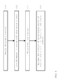
- FIG. 6 illustrates an example of a method for deep discharge protection.
- the chargeable battery 1 may be charged (step 601).
- the charging may be performed by a battery charging unit 2 which is coupled to the chargeable battery 1 and which includes an internal switch S2. It is, however, also possible that the charging is performed by some external charging unit and the chargeable battery 1 is already partly or completely charged when it is coupled to the internal charging unit.
- the chargeable battery 1 may then be used to provide energy to the system 3 (step 602), when no other energy source, such as a vehicle battery for example, is available and an operation of the system is needed.
- the voltage of the chargeable battery 1 is monitored (step 603). The monitoring is performed irrespective of a use of the chargeable battery 1, meaning that the monitoring is performed while the chargeable battery 1 powers the system 3, as well as while the chargeable battery 1 is not used to power the system. This is because the chargeable battery 1 also discharges steadily, even if it is not used to power the system.
- An opening of an internal switch S2 of a battery charging unit 2 may be triggered (step 604), wherein the battery charging unit 2 is coupled to the chargeable battery 1, and wherein the chargeable battery 1 is disconnected from the system 3 when the at least one internal switch S2 is opened.
- the opening of the internal switch S2 of the battery charging unit 2 may, for example, be triggered when the battery voltage falls below a predefined threshold voltage. It is, however, also possible to open the internal switch S2 of the battery charging unit 2 after the first insertion of the chargeable battery 1 in the electronic device at the end of the production line and before connecting the electronic device to an external energy source.
- the chargeable battery 1 may be a lithium-ion battery, for example, as has already been described above.
- the chargeable battery1 may be any other kind of chargeable battery, such as a nickel-cadmium battery, for example.
Landscapes
- Engineering & Computer Science (AREA)
- Power Engineering (AREA)
- Charge And Discharge Circuits For Batteries Or The Like (AREA)
Abstract
Description
- The current invention refers to a system and a method for deep discharge protection of a battery, particularly of a lithium-ion battery.
- Rechargeable lithium-ion (li-ion) batteries are used for many different applications, e.g. in consumer and automotive electronics. For example, a li-ion battery may be used for powering a so-called on-board unit. In many countries all over the world there are toll roads (also known as turnpikes or tollways), for which a fee (or toll) is assessed for passage. Different systems for collecting the toll are known, for example electronic road toll systems. In electronic road toll systems an on-board unit is installed in the vehicle to determine the position of the vehicle and transmit position data to a central office for billing.
- In li-ion batteries, lithium ions move from a negative electrode to a positive electrode during discharge and from the positive electrode to the negative electrode when charging. It should be avoided to completely discharge a li-ion battery (deep discharge), as this could lead to permanent damage of the battery. Therefore, deep discharge protection circuits are known. Such deep discharge protection circuits generally include a switch, mostly a transistor, which disconnects the battery from the system, when the battery voltage decreases below a certain level. The transistors, which are used as switches, are usually power MOS-transistors (MOS = metal oxide semiconductor). The transistors are generally arranged between a battery charging unit and the battery itself. During normal operation of the charging unit, a voltage is provided at an output of the charging circuit for charging the battery. This leads to a voltage drop across the transistor, which in turn leads to a heating of the transistor and, therefore, of the whole charging unit. Further, the system does not easily start up again once the transistor disconnects the battery from the charging unit (transistor is non-conducting), even if the system is connected to a vehicle battery.
- The problem to be solved by the current invention is, therefore, to provide a system and a method for deep discharge protection of a battery which overcomes the above disadvantages.
- This problem is solved by a system according to
claim 1 and a method according to claim 11. Configurations and further developments of the invention are subject of the dependent claims. - A system for deep discharge protection of a chargeable battery in an electronic device comprises a chargeable battery, which is configured to provide energy to a system, when operation of the electronic device is needed and no other energy source is available. The system further comprises a battery charging unit with an internal switch, wherein the battery charging unit is coupled to the chargeable battery and is configured to charge the chargeable battery. The system further comprises a deep discharge protection unit and a transport mode unit. The discharge protection unit is configured to monitor a voltage of the chargeable battery and disconnect the chargeable battery from the system, when the battery voltage is lower than a given threshold voltage and the transport mode unit is configured to trigger an opening the internal switch of the battery charging unit, wherein the chargeable battery is disconnected from the system when the at least one switch is opened.
- The deep discharge protection unit may be configured to trigger an opening of the internal switch of the battery charging unit when the battery voltage is lower than the given threshold voltage. A deep discharge of the chargeable battery may therefore be prevented during the normal operation of the electronic device.
- Alternatively or additionally, an opening of the internal switch may be triggered after the first insertion of the chargeable battery in the electronic device at the end of the production line and before connecting the electronic device to an external energy source. As it is usually not known how long it takes from production to the first use of a device, a deep discharge during shipment of the device may be prevented.
- In this way a deep discharge of the chargeable battery may be prevented during shipment of a device, when it is already inserted in an electronic device. As an internal switch is already included in most battery charging units, no additional expensive and/or large switches are needed.
- The electronic device may be mounted in a vehicle and the external energy source is a vehicle battery. In particular, the electronic device may be an on-board unit.
- The system may comprise a controller, which is configured to enable or disable a charging of the chargeable battery. The controller may be configured to receive a manual input, which indicates that a disconnection of the chargeable battery from the system is desired. For example, an operator may instruct the controller at the end of the production line to disconnect the chargeable battery from the system.
- The controller may be further configured to output a transport signal, when a manual input is received, wherein the transport signal triggers an opening of the internal switch of the battery charging unit.
- The internal switch may be closed and the chargeable battery coupled to the system again, when the electronic device is coupled to the external energy source. No further command is needed to return the system from the transport mode to a running mode. A customer may resume the functionalities of the system by simply plugging it to an energy source.
- The battery may be a lithium-ion or a nickel-cadmium battery. Such batteries may be charged. They have a very high energy density compared to other batteries. Further, lithium-ion batteries may be charged up to comparably high voltages.
- A method for deep discharge protection of a chargeable battery in an electronic device comprises charging the chargeable battery by means of a battery charging unit which is coupled to the chargeable battery and which comprises an internal switch. The method further comprises using the chargeable battery to provide energy to a system, when operation of the electronic device is needed and no other energy source than the chargeable battery is available, monitoring a voltage of the chargeable battery and disconnecting the chargeable battery from the system, when the battery voltage is lower than a given threshold voltage. An opening of the internal switch of the battery charging unit is triggered, wherein the chargeable battery is disconnected from the system when the at least one switch is opened.
- An opening of the internal switch of the battery charging unit may be triggered when the battery voltage is lower than the given threshold voltage.
- Additionally or alternatively, an opening of the internal switch may be triggered after the first insertion of the chargeable battery in the electronic device at the end of the production line and before connecting the electronic device to an external energy source.
- Examples are now explained with reference to the drawings. In the drawings the same reference characters denote like features.
-
Figure 1 schematically illustrates in a block diagram an example of a battery charging circuit, -
Figure 2 schematically illustrates in a block diagram a system for deep discharge protection according to one example of the present invention, -
Figure 3 schematically illustrates an example of a charging unit according to the present invention, -
Figure 4 schematically illustrates an example of a transport mode unit according to the present invention, -
Figure 5 schematically illustrates an example of a deep discharge protection unit according to the present invention, -
Figure 6 an example of a method for deep discharge protection according to the present invention. -
Figure 1 illustrates in a block diagram a battery charging circuit. The battery charging circuit includes achargeable battery 1, which may be a lithium-ion (li-ion) battery. With a first output, thechargeable battery 1 is coupled to a second terminal V2 for a second potential, which may be ground, for example. Abattery charging unit 2 is coupled between a second output of thechargeable battery 1 and a first terminal V1 for a first potential. The first terminal V1 may be coupled to a vehicle battery, for example. More precisely, the first terminal V1 may be coupled to what is generally known as terminal 30. The battery charging circuit may be integrated in an electronic device such as an on-board unit, for example. An on-board unit usually is configured to determine the position of a vehicle in regular intervals and provide this position data to a central office for billing. Therefore, one or more devices (e.g. controllers), which perform the functionalities of the electronic device, are further included in the battery charging circuit. Such devices are represented as thesystem 3, which is coupled to thebattery charging unit 2. Thesystem 3 may be powered by the vehicle battery or, if the vehicle battery is not connected, by thechargeable battery 1. - The
battery charging unit 2 is configured to provide power to thesystem 3, as well as to charge thechargeable battery 1, if desired. It is possible that at one point, thebattery charging unit 2 only provides power to thesystem 3, but battery charging is disabled (e.g. when the chargeable battery is fully charged). It is, however, also possible that thebattery charging unit 2 provides power to thesystem 3 and at the same time charges thechargeable battery 1. Further, it is possible that the battery charging unit charges thechargeable battery 1, while no power is provided to thesystem 3. - The
system 3 may include a controller (not illustrated inFigure 1 ), which is configured to enable thebattery charging unit 2 to charge thechargeable battery 1, if charging of thechargeable battery 1 is required. The controller may be further configured to disable thebattery charging unit 2, if charging of thechargeable battery 1 is not required. - To protect the
chargeable battery 1 from completely discharging (deep discharge), a deepdischarge protection unit 4 is included in the battery charging circuit ofFigure 1 . The deepdischarge protection unit 4 is configured to determine a voltage of thechargeable battery 1. Everychargeable battery 1 may be charged up to a maximum voltage, e.g. 4.2V. When thechargeable battery 1 powers asystem 3, the battery voltage decreases. The deepdischarge protection unit 4 is further configured to compare the determined battery voltage to a predetermined threshold voltage. If the battery voltage falls below the threshold voltage, thechargeable battery 1 is disconnected from thesystem 3 by means of a switch S1. The switch S1 may be a power MOS-transistor, for example. When disconnected from thesystem 3, no more energy is provided to thesystem 3 and any other components and deep discharge may be prevented. - Before electronic devices are used for the first time after production, usually a certain time passes (e.g. during shipment of the devices). It is often desired to provide electronic devices already including the chargeable battery. This is because in some industries such as the automotive industry, for example, special connections or contacts are used. Therefore, it might be more convenient for a user to have a battery with matching connections or contacts already inserted. However, if the time between production and use (e.g. installation of an on-board unit in a vehicle) is too long, and the battery is already connected to the system, the battery might be completely discharged, which may cause fatal damages of the battery. It is therefore desired to disconnect the chargeable battery from the rest of the system as long as it is not connected to the vehicle battery. The switch S1, therefore, may be opened during the delivery of the devices, and may be closed once the on-board unit is connected to the vehicle battery.
- The battery charging circuit illustrated in
Figure 1 , especially the switch S1, which is coupled between thesystem 3 and thebattery charging unit 2, has several drawbacks. In particular, the switch S1, which is usually implemented as a transistor, needs to be a rather big and, therefore, expensive switch (e.g. power transistor) in order to sufficiently protect thechargeable battery 1 from discharging. - In the system for deep discharge protection of a chargeable battery according to the present invention, therefore, the switch S1 is omitted. Such a system is schematically illustrated in
Figure 2 . In addition to the components already explained by means ofFigure 1 a transport mode unit 5 is coupled between the deepdischarge protection unit 4 and the first terminal V1. The transport mode unit 5 is configured to initiate a disconnection of thechargeable battery 1 from the other components, especially from thesystem 3. According to the present invention, when disconnecting thechargeable battery 1 from thesystem 3, the chargingunit 2 functions as a switching device. Therefore, the chargingunit 2 includes at least one internal switch S2. By opening this at least one internal switch S2, thechargeable battery 1 may be disconnected from the rest of the battery charging system. Many battery charging ICs (integrated circuits) available today already include a internal switch S2, which may be used to disconnect thechargeable battery 1. Thechargeable battery 1, by means of that internal switch S2, may be disconnected from thesystem 3 during transportation from the manufacturer of the on-board unit until its installation in a vehicle. The internal switch S2, however, may also be used to disconnect thechargeable battery 1 from thesystem 3 after installation in a vehicle, when the battery voltage falls below a certain threshold. - During or at the end of the production of the on-board unit, the
chargeable battery 1 will be inserted in the on-board unit. Usually, at this point, thechargeable battery 1 is partly or completely charged. When the on-board unit is delivered to a customer, thechargeable battery 1 will provide at least a small amount of power to the other components of the on-board unit (the system 3). If the on-board unit is not connected to a vehicle battery after a certain time, thechargeable battery 1 may be completely discharged and, therefore, may be damaged. Therefore, after inserting the chargeable battery in the on-board unit, thesystem 3 may send a first transport signal TS to the transport mode unit 5. The transport mode unit 5 again sends a second signal X1 to the deepdischarge protection unit 4. This results in a third signal DIS being sent to thecharging unit 2. This third signal DIS causes thecharging unit 2 to decouple thechargeable battery 1 from thesystem 3 by opening the internal switch S2. The on-board unit at this moment enters a transportation mode. - When the on-board unit is mounted on a vehicle and the vehicle battery is connected to the on-board unit (terminal V1 of the battery charging system will be connected to the vehicle battery), the
chargeable battery 1 will again be coupled to thesystem 3. By connecting the vehicle battery, the on-board unit will exit the transportation mode and resume its normal operation. -
Figure 3 illustrates one example of acharging unit 2 in greater detail. The chargingunit 2 includes a charging IC 21 (integrated circuit). Charging ICs are special devices, which are configured to enable or disable the charging of achargeable battery 1. Charging ICs are offered by several different semiconductor companies. Each chargingIC 21 usually requires an individual wiring of the different pins. Generally some kind of protection circuitry is needed or components such as resistors and capacitors have to be connected to certain pins, in order to enable certain functionalities of the chargingIC 21. The particular wiring depends on the model of the charging IC. Therefore, the circuit illustrated inFigure 3 is only an example. The chargingunit 2 may be implemented in any other suitable way. In the circuit illustrated inFigure 3 , pins and components, which are not needed for the current invention but might be included in a chargingIC 21 are omitted. - The charging
IC 21 may be coupled to the second terminal V2, which may be ground, for example, with a first pin VSS. At a second pin SYSOFF, the chargingIC 21 may receive a signal BAT_DIS. The second pin SYSOFF may be a system enable input, for example. If the signal BAT_DIS is provided to the second pin SYSOFF, thechargeable battery 1 is connected to thesystem 3. This may be the case when the vehicle battery is not available for any reason. Thechargeable battery 1 may be connected to a third pin BAT of the chargingIC 21. A voltage divider including resistors R2, R2 and capacitors C6, C7, C8 may be coupled between thebattery 1 and the third pin. In this way, a voltage of thebattery 1 may be monitored. If the voltage falls below a certain threshold, thebattery 1 may be disconnected from thesystem 3, e.g. by opening the internal switch S2 (not illustrated inFigure 3 ). With a fourth pin OUT, thechargeable IC 21 may be coupled to thesystem 3. Three capacitors C3, C4 and C5 are coupled in parallel between a common node between thesystem 3 and the chargingIC 21 and the second terminal V2 (e.g. ground). The capacitors may prevent a fluctuating voltage at the fourth pin OUT and ensure a stable operation of the chargingIC 21. - A fifth pin IN is coupled to the first terminal V1 (e.g. vehicle battery). Two capacitors C1 and C2 are coupled in parallel between a common node between the fifth pin IN and the first terminal V1 and the second terminal V2. A resistor R1 is coupled between the fifth pin IN and a sixth pin CE. A transistor T1 is coupled between a common node between the sixth pin CE and the resistor R1 and the second terminal V2 with its load path. At a control terminal, the transistor T1 receives a signal B_STOP. Depending on the signal B_STOP, the transistor T1 is either conducting or non-conducting. For example, the transistor T1 may be conducting, when the signal B_STOP takes on a logic High level (or a logic Low level). The sixth pin CE is then coupled to the second terminal V2 via the transistor T1. This results in a logic High level (or a logic Low level, respectively) being received at the sixth pin CE. This will transfer the charging
IC 21 to a standby mode. In standby mode, an internal switch of the chargingIC 21 is opened, which disconnects thechargeable battery 1 from thesystem 3 and from the first terminal V1. Thechargeable battery 1 will not be charged during standby mode and thesystem 3 will not be provided with energy. - In
Figure 4 , one specific example of a transport mode unit 5 is illustrated. The circuit illustrated inFigure 4 , however, is only an example to further describe the general functionality of the battery charging system. The transport mode unit 5 may be implemented in any other suitable way. If a transport signal is received at the terminal TS, or if the transport signal takes on a certain level, e.g. logic High (or Low, respectively), the signal at terminal X1 changes its state (e.g. from logic High to logic Low or vice versa). The transport signal TS may be provided by thesystem 3, for example. In particular, a controller of thesystem 3 may generate signal TS at the end of the production line, before the on-board unit is sent to a customer for installation. The terminal X1 is coupled to the deepdischarge protection unit 4, as will be further explained by means ofFigure 5 . The transport mode unit 5 is both coupled to thechargeable battery 1 and thesystem 3. The circuit illustrated inFigure 4 acts as a bistable circuit. The circuit ofFigure 4 illustrates a circuit which is easy to implement, using rather cheap and simple components. Further, the circuit has a very low quiescent current compared to other circuits. As the circuit diagram inFigure 4 is only one example out of many of an implementation of a transport mode unit 5, the exact function of the different components will not be described in further detail. - An example for a deep
discharge protection unit 4 is illustrated inFigure 5 . As long as the signal at terminal X1 (received from the transport mode unit 5) is in a fist state (e.g. High), thechargeable battery 1 is coupled to thesystem 3. If the signal at terminal X1 changes its state, a signal B_STOP will be output to thecharging unit 2, as has been described by means ofFigure 3 . Thechargeable battery 1 will then be disconnected from the system, by opening an internal switch of the chargingunit 2. In the circuit ofFigure 5 , thevoltage monitoring unit 51 becomes conductive, if a voltage of the chargeable battery is above a certain threshold (e.g. 3.3V). Thevoltage monitoring unit 51, therefore, may include some kind of comparator, which compares the battery voltage to a predefined threshold voltage. If thevoltage monitoring unit 51 is conductive, transistor T8 will be coupled to the second terminal V2. If at the same time signal X1 is low (or high, respectively, depending on which kind of transistor is used) the transistor T8 is non-conductive. Transistor T9, on the other hand, would be conductive. If signal X1 is High (or low, respectively), the transistor T10 will become conductive. If both transistors T9 and T10 are conductive, the output signal B_STOP will be low. As long as signal B_STOP is low, the chargingIC 21 will provide power to the system 3 (as has been explained by means ofFigure 3 ). - When put in the transport mode, signal X1 will get Low. Transistor T10 would then be non-conductive and, accordingly, output signal B_STOP will be High. The charging
IC 21 will then stop supplying power to thesystem 3 and the internal switch S2 of the chargingIC 21 will be opened. - Once the on-board unit is coupled to a vehicle battery, a voltage is received at terminal V1. This results in the
chargeable battery 1 being again coupled to thesystem 3. It is also possible to restore the functionality of the battery charging system by plugging the on-board unit to a cigarette lighter of a vehicle. This also results in a voltage, which is supplied at the first terminal V1. -
Figure 6 illustrates an example of a method for deep discharge protection. In a first step, thechargeable battery 1 may be charged (step 601). The charging may be performed by abattery charging unit 2 which is coupled to thechargeable battery 1 and which includes an internal switch S2. It is, however, also possible that the charging is performed by some external charging unit and thechargeable battery 1 is already partly or completely charged when it is coupled to the internal charging unit. - The
chargeable battery 1 may then be used to provide energy to the system 3 (step 602), when no other energy source, such as a vehicle battery for example, is available and an operation of the system is needed. The voltage of thechargeable battery 1 is monitored (step 603). The monitoring is performed irrespective of a use of thechargeable battery 1, meaning that the monitoring is performed while thechargeable battery 1 powers thesystem 3, as well as while thechargeable battery 1 is not used to power the system. This is because thechargeable battery 1 also discharges steadily, even if it is not used to power the system. - An opening of an internal switch S2 of a
battery charging unit 2 may be triggered (step 604), wherein thebattery charging unit 2 is coupled to thechargeable battery 1, and wherein thechargeable battery 1 is disconnected from thesystem 3 when the at least one internal switch S2 is opened. The opening of the internal switch S2 of thebattery charging unit 2 may, for example, be triggered when the battery voltage falls below a predefined threshold voltage. It is, however, also possible to open the internal switch S2 of thebattery charging unit 2 after the first insertion of thechargeable battery 1 in the electronic device at the end of the production line and before connecting the electronic device to an external energy source. - The
chargeable battery 1 may be a lithium-ion battery, for example, as has already been described above. The chargeable battery1, however, may be any other kind of chargeable battery, such as a nickel-cadmium battery, for example.
Claims (13)
- System for deep discharge protection of a chargeable battery (1) in an electronic device, the system comprises:a chargeable battery (1), which is configured to provide energy to a system (3), when operation of the electronic device is needed and no other energy source is available;a battery charging unit (2) with an internal switch (S2), wherein the battery charging unit (2) is coupled to the chargeable battery (1) and is configured to charge the chargeable battery (1);a deep discharge protection unit (4), which is configured to monitor a voltage of the chargeable battery (1) and disconnect the chargeable battery (1) from the system (3), when the battery voltage is lower than a given threshold voltage; anda transport mode unit (5), which is configured to trigger an opening of the internal switch (S2) of the battery charging unit (2), wherein the chargeable battery (1) is disconnected from the system (3) when the at least one internal switch (S2) is opened.
- System according to claim 1, wherein the deep discharge protection unit (4) is further configured to trigger an opening of the internal switch (S2) of the battery charging unit (2) when the battery voltage is lower than the given threshold voltage.
- System according to claim 1 or 2, wherein an opening of the internal switch (S2) is triggered after the first insertion of the chargeable battery (1) in the electronic device at the end of the production line and before connecting the electronic device to an external energy source.
- System according to claim 3, wherein the electronic device is mounted in a vehicle and the external energy source is a vehicle battery.
- System according to any of claims 1 to 4, wherein the electronic device is an on-board unit.
- System according to any of claims 1 to 5, wherein the system (3) comprises a controller, which is configured to enable or disable a charging of the chargeable battery (1).
- System according to claim 6, wherein the controller is further configured to receive a manual input, which indicates that a disconnection of the chargeable battery (1) from the system (3) is desired.
- System according to claim 7, wherein the controller is further configured to output a transport signal (TS), when a manual input is received, wherein the transport signal (TS) triggers an opening of the internal switch (S2) of the battery charging unit (2).
- System according to any of the preceding claims, wherein the internal switch (S2) is closed and the chargeable battery (1) is coupled to the system (3) again, when the electronic device is coupled to the external energy source.
- System according to any of the preceding claims, wherein the battery (1) is a lithium-ion or a nickel-cadmium battery.
- Method for deep discharge protection of a chargeable battery (1) in an electronic device, the method comprises:charging the chargeable battery (1);using the chargeable battery (1) to provide energy to a system (3), when operation of the electronic device is needed and no other energy source than the chargeable battery (1) is available;monitoring a voltage of the chargeable battery (1) and disconnecting the chargeable battery (1) from the system (3), when the battery voltage is lower than a given threshold voltage; andtriggering an opening of an internal switch (S2) of a battery charging unit (2), wherein the battery charging unit (2) is coupled to the chargeable battery (1), and wherein the chargeable battery (1) is disconnected from the system (3) when the at least one internal switch (S2) is opened.
- Method according to claim 11, wherein an opening of the internal switch (S2) of the battery charging unit (2) is triggered when the battery voltage is lower than the given threshold voltage.
- Method according to claim 11 or 12, wherein an opening of the internal switch (S2) is triggered after the first insertion of the chargeable battery (1) in the electronic device at the end of the production line and before connecting the electronic device to an external energy source.
Priority Applications (1)
| Application Number | Priority Date | Filing Date | Title |
|---|---|---|---|
| EP15465549.2A EP3154149B1 (en) | 2015-10-09 | 2015-10-09 | System and method for deep discharge protection of a battery |
Applications Claiming Priority (1)
| Application Number | Priority Date | Filing Date | Title |
|---|---|---|---|
| EP15465549.2A EP3154149B1 (en) | 2015-10-09 | 2015-10-09 | System and method for deep discharge protection of a battery |
Publications (2)
| Publication Number | Publication Date |
|---|---|
| EP3154149A1 true EP3154149A1 (en) | 2017-04-12 |
| EP3154149B1 EP3154149B1 (en) | 2023-12-06 |
Family
ID=54601725
Family Applications (1)
| Application Number | Title | Priority Date | Filing Date |
|---|---|---|---|
| EP15465549.2A Active EP3154149B1 (en) | 2015-10-09 | 2015-10-09 | System and method for deep discharge protection of a battery |
Country Status (1)
| Country | Link |
|---|---|
| EP (1) | EP3154149B1 (en) |
Cited By (1)
| Publication number | Priority date | Publication date | Assignee | Title |
|---|---|---|---|---|
| AU2020100837B4 (en) * | 2019-05-27 | 2021-02-11 | Einhell Germany Ag | Switching of several variables in the transport mode |
Citations (3)
| Publication number | Priority date | Publication date | Assignee | Title |
|---|---|---|---|---|
| US20130229145A1 (en) * | 2012-03-02 | 2013-09-05 | Stmicroelectronics S.R.I. | Battery charger |
| US20150022956A1 (en) * | 2013-07-16 | 2015-01-22 | Texas Instruments Incorporated | Electronic Pull Tab for Battery Protection |
| CN204331839U (en) * | 2015-01-07 | 2015-05-13 | 深圳市金溢科技股份有限公司 | For the hand-held device that board units is issued online |
Family Cites Families (3)
| Publication number | Priority date | Publication date | Assignee | Title |
|---|---|---|---|---|
| JP3380766B2 (en) * | 1999-03-18 | 2003-02-24 | 富士通株式会社 | Protection method, control circuit, and battery unit |
| US6903533B1 (en) * | 2003-12-16 | 2005-06-07 | Motorola, Inc. | Power fault battery protection circuit |
| US8729863B2 (en) * | 2009-07-10 | 2014-05-20 | Motorola Mobility Llc | Battery and energy management circuit with temporal storage mode |
-
2015
- 2015-10-09 EP EP15465549.2A patent/EP3154149B1/en active Active
Patent Citations (3)
| Publication number | Priority date | Publication date | Assignee | Title |
|---|---|---|---|---|
| US20130229145A1 (en) * | 2012-03-02 | 2013-09-05 | Stmicroelectronics S.R.I. | Battery charger |
| US20150022956A1 (en) * | 2013-07-16 | 2015-01-22 | Texas Instruments Incorporated | Electronic Pull Tab for Battery Protection |
| CN204331839U (en) * | 2015-01-07 | 2015-05-13 | 深圳市金溢科技股份有限公司 | For the hand-held device that board units is issued online |
Cited By (1)
| Publication number | Priority date | Publication date | Assignee | Title |
|---|---|---|---|---|
| AU2020100837B4 (en) * | 2019-05-27 | 2021-02-11 | Einhell Germany Ag | Switching of several variables in the transport mode |
Also Published As
| Publication number | Publication date |
|---|---|
| EP3154149B1 (en) | 2023-12-06 |
Similar Documents
| Publication | Publication Date | Title |
|---|---|---|
| KR102285228B1 (en) | Secondary battery protection circuit, secondary battery protection device, battery pack and method of controlling secondary battery protection circuit | |
| US10622819B2 (en) | Rechargeable battery protection integrated circuit, rechargeable battery protection device, and battery pack | |
| US10516276B2 (en) | Secondary battery protecting integrated circuit, secondary battery protecting circuit, charge control circuit, and battery pack | |
| US5990663A (en) | Charge/discharge control circuit and charging type power-supply unit | |
| CN102983555B (en) | Semiconductor integrated circuit, protection circuit and battery pack | |
| CN104022542B (en) | Charge-discharge control circuit and charge/discharge control method | |
| CN101055999B (en) | Charge/discharge protection circuit and power-supply unit | |
| KR101784740B1 (en) | Battery protection circuit and battery pack including same | |
| KR100871573B1 (en) | Charge/discharge protection circuit for a rechargeable battery | |
| US9081069B2 (en) | Protection IC and method of monitoring a battery voltage | |
| KR100991634B1 (en) | Overvoltage Protected Battery Chargers and Associated Methods | |
| US8896270B2 (en) | Semiconductor integrated circuit, protection circuit, and battery pack | |
| CN104022541B (en) | Charge-discharge control circuit and cell apparatus | |
| US8581556B2 (en) | Protection circuit and battery pack having current varying circuit to vary current flowing through power terminal | |
| CN103746347A (en) | Battery protection chip and battery system | |
| CN110875619A (en) | Secondary battery protection device, protection circuit and control method thereof, battery pack | |
| JP2003259546A (en) | Charge / discharge protection circuit for secondary battery | |
| EP2365602A2 (en) | Battery pack charger | |
| US6111388A (en) | Charge and discharge control circuit | |
| WO2011050189A1 (en) | Circuitry for balancing charging of series connected battery cells | |
| KR20110043473A (en) | Battery condition monitoring circuit and battery unit | |
| EP3154149B1 (en) | System and method for deep discharge protection of a battery | |
| CN215990263U (en) | Integrated circuit and system for battery charging and discharging protection | |
| KR101892964B1 (en) | Semiconductor integrated circuit, protection circuit and battery pack | |
| CN113169564A (en) | Battery pack and electrical equipment system |
Legal Events
| Date | Code | Title | Description |
|---|---|---|---|
| PUAI | Public reference made under article 153(3) epc to a published international application that has entered the european phase |
Free format text: ORIGINAL CODE: 0009012 |
|
| STAA | Information on the status of an ep patent application or granted ep patent |
Free format text: STATUS: THE APPLICATION HAS BEEN PUBLISHED |
|
| AK | Designated contracting states |
Kind code of ref document: A1 Designated state(s): AL AT BE BG CH CY CZ DE DK EE ES FI FR GB GR HR HU IE IS IT LI LT LU LV MC MK MT NL NO PL PT RO RS SE SI SK SM TR |
|
| AX | Request for extension of the european patent |
Extension state: BA ME |
|
| STAA | Information on the status of an ep patent application or granted ep patent |
Free format text: STATUS: REQUEST FOR EXAMINATION WAS MADE |
|
| 17P | Request for examination filed |
Effective date: 20171012 |
|
| RBV | Designated contracting states (corrected) |
Designated state(s): AL AT BE BG CH CY CZ DE DK EE ES FI FR GB GR HR HU IE IS IT LI LT LU LV MC MK MT NL NO PL PT RO RS SE SI SK SM TR |
|
| RAP1 | Party data changed (applicant data changed or rights of an application transferred) |
Owner name: CONTINENTAL AUTOMOTIVE GMBH |
|
| STAA | Information on the status of an ep patent application or granted ep patent |
Free format text: STATUS: EXAMINATION IS IN PROGRESS |
|
| 17Q | First examination report despatched |
Effective date: 20210211 |
|
| RAP1 | Party data changed (applicant data changed or rights of an application transferred) |
Owner name: CONTINENTAL AUTOMOTIVE TECHNOLOGIES GMBH |
|
| GRAP | Despatch of communication of intention to grant a patent |
Free format text: ORIGINAL CODE: EPIDOSNIGR1 |
|
| STAA | Information on the status of an ep patent application or granted ep patent |
Free format text: STATUS: GRANT OF PATENT IS INTENDED |
|
| INTG | Intention to grant announced |
Effective date: 20230629 |
|
| P01 | Opt-out of the competence of the unified patent court (upc) registered |
Effective date: 20230712 |
|
| GRAS | Grant fee paid |
Free format text: ORIGINAL CODE: EPIDOSNIGR3 |
|
| GRAA | (expected) grant |
Free format text: ORIGINAL CODE: 0009210 |
|
| STAA | Information on the status of an ep patent application or granted ep patent |
Free format text: STATUS: THE PATENT HAS BEEN GRANTED |
|
| AK | Designated contracting states |
Kind code of ref document: B1 Designated state(s): AL AT BE BG CH CY CZ DE DK EE ES FI FR GB GR HR HU IE IS IT LI LT LU LV MC MK MT NL NO PL PT RO RS SE SI SK SM TR |
|
| REG | Reference to a national code |
Ref country code: GB Ref legal event code: FG4D |
|
| REG | Reference to a national code |
Ref country code: CH Ref legal event code: EP |
|
| REG | Reference to a national code |
Ref country code: DE Ref legal event code: R096 Ref document number: 602015086810 Country of ref document: DE |
|
| REG | Reference to a national code |
Ref country code: IE Ref legal event code: FG4D |
|
| REG | Reference to a national code |
Ref country code: DE Ref legal event code: R081 Ref document number: 602015086810 Country of ref document: DE Owner name: CONTINENTAL AUTOMOTIVE TECHNOLOGIES GMBH, DE Free format text: FORMER OWNER: CONTINENTAL AUTOMOTIVE TECHNOLOGIES GMBH, 30165 HANNOVER, DE Ref country code: DE Ref legal event code: R081 Ref document number: 602015086810 Country of ref document: DE Owner name: AUMOVIO GERMANY GMBH, DE Free format text: FORMER OWNER: CONTINENTAL AUTOMOTIVE TECHNOLOGIES GMBH, 30165 HANNOVER, DE |
|
| REG | Reference to a national code |
Ref country code: LT Ref legal event code: MG9D |
|
| PG25 | Lapsed in a contracting state [announced via postgrant information from national office to epo] |
Ref country code: GR Free format text: LAPSE BECAUSE OF FAILURE TO SUBMIT A TRANSLATION OF THE DESCRIPTION OR TO PAY THE FEE WITHIN THE PRESCRIBED TIME-LIMIT Effective date: 20240307 |
|
| REG | Reference to a national code |
Ref country code: NL Ref legal event code: MP Effective date: 20231206 |
|
| PG25 | Lapsed in a contracting state [announced via postgrant information from national office to epo] |
Ref country code: LT Free format text: LAPSE BECAUSE OF FAILURE TO SUBMIT A TRANSLATION OF THE DESCRIPTION OR TO PAY THE FEE WITHIN THE PRESCRIBED TIME-LIMIT Effective date: 20231206 |
|
| RAP4 | Party data changed (patent owner data changed or rights of a patent transferred) |
Owner name: CONTINENTAL AUTOMOTIVE TECHNOLOGIES GMBH |
|
| PG25 | Lapsed in a contracting state [announced via postgrant information from national office to epo] |
Ref country code: ES Free format text: LAPSE BECAUSE OF FAILURE TO SUBMIT A TRANSLATION OF THE DESCRIPTION OR TO PAY THE FEE WITHIN THE PRESCRIBED TIME-LIMIT Effective date: 20231206 |
|
| PG25 | Lapsed in a contracting state [announced via postgrant information from national office to epo] |
Ref country code: LT Free format text: LAPSE BECAUSE OF FAILURE TO SUBMIT A TRANSLATION OF THE DESCRIPTION OR TO PAY THE FEE WITHIN THE PRESCRIBED TIME-LIMIT Effective date: 20231206 Ref country code: GR Free format text: LAPSE BECAUSE OF FAILURE TO SUBMIT A TRANSLATION OF THE DESCRIPTION OR TO PAY THE FEE WITHIN THE PRESCRIBED TIME-LIMIT Effective date: 20240307 Ref country code: ES Free format text: LAPSE BECAUSE OF FAILURE TO SUBMIT A TRANSLATION OF THE DESCRIPTION OR TO PAY THE FEE WITHIN THE PRESCRIBED TIME-LIMIT Effective date: 20231206 Ref country code: BG Free format text: LAPSE BECAUSE OF FAILURE TO SUBMIT A TRANSLATION OF THE DESCRIPTION OR TO PAY THE FEE WITHIN THE PRESCRIBED TIME-LIMIT Effective date: 20240306 |
|
| REG | Reference to a national code |
Ref country code: CH Ref legal event code: PK Free format text: DIE PUBLIKATION VOM 27.03.2024 WURDE AM 24.04.2024 IRRTUEMLICHERWEISE ERNEUT PUBLIZIERT. LA PUBLICATION DU 27.03.2024 A ETE REPUBLIEE PAR ERREUR LE 24.04.2024. LA PUBBLICAZIONE DEL 27.03.2024 E STATA ERRONEAMENTE RIPUBBLICATA IL 24.04.2024. |
|
| REG | Reference to a national code |
Ref country code: AT Ref legal event code: MK05 Ref document number: 1639325 Country of ref document: AT Kind code of ref document: T Effective date: 20231206 |
|
| PG25 | Lapsed in a contracting state [announced via postgrant information from national office to epo] |
Ref country code: NL Free format text: LAPSE BECAUSE OF FAILURE TO SUBMIT A TRANSLATION OF THE DESCRIPTION OR TO PAY THE FEE WITHIN THE PRESCRIBED TIME-LIMIT Effective date: 20231206 |
|
| PG25 | Lapsed in a contracting state [announced via postgrant information from national office to epo] |
Ref country code: SE Free format text: LAPSE BECAUSE OF FAILURE TO SUBMIT A TRANSLATION OF THE DESCRIPTION OR TO PAY THE FEE WITHIN THE PRESCRIBED TIME-LIMIT Effective date: 20231206 Ref country code: RS Free format text: LAPSE BECAUSE OF FAILURE TO SUBMIT A TRANSLATION OF THE DESCRIPTION OR TO PAY THE FEE WITHIN THE PRESCRIBED TIME-LIMIT Effective date: 20231206 Ref country code: NO Free format text: LAPSE BECAUSE OF FAILURE TO SUBMIT A TRANSLATION OF THE DESCRIPTION OR TO PAY THE FEE WITHIN THE PRESCRIBED TIME-LIMIT Effective date: 20240306 Ref country code: NL Free format text: LAPSE BECAUSE OF FAILURE TO SUBMIT A TRANSLATION OF THE DESCRIPTION OR TO PAY THE FEE WITHIN THE PRESCRIBED TIME-LIMIT Effective date: 20231206 Ref country code: LV Free format text: LAPSE BECAUSE OF FAILURE TO SUBMIT A TRANSLATION OF THE DESCRIPTION OR TO PAY THE FEE WITHIN THE PRESCRIBED TIME-LIMIT Effective date: 20231206 Ref country code: HR Free format text: LAPSE BECAUSE OF FAILURE TO SUBMIT A TRANSLATION OF THE DESCRIPTION OR TO PAY THE FEE WITHIN THE PRESCRIBED TIME-LIMIT Effective date: 20231206 |
|
| PG25 | Lapsed in a contracting state [announced via postgrant information from national office to epo] |
Ref country code: IS Free format text: LAPSE BECAUSE OF FAILURE TO SUBMIT A TRANSLATION OF THE DESCRIPTION OR TO PAY THE FEE WITHIN THE PRESCRIBED TIME-LIMIT Effective date: 20240406 |
|
| PG25 | Lapsed in a contracting state [announced via postgrant information from national office to epo] |
Ref country code: AT Free format text: LAPSE BECAUSE OF FAILURE TO SUBMIT A TRANSLATION OF THE DESCRIPTION OR TO PAY THE FEE WITHIN THE PRESCRIBED TIME-LIMIT Effective date: 20231206 Ref country code: CZ Free format text: LAPSE BECAUSE OF FAILURE TO SUBMIT A TRANSLATION OF THE DESCRIPTION OR TO PAY THE FEE WITHIN THE PRESCRIBED TIME-LIMIT Effective date: 20231206 |
|
| PG25 | Lapsed in a contracting state [announced via postgrant information from national office to epo] |
Ref country code: SK Free format text: LAPSE BECAUSE OF FAILURE TO SUBMIT A TRANSLATION OF THE DESCRIPTION OR TO PAY THE FEE WITHIN THE PRESCRIBED TIME-LIMIT Effective date: 20231206 |
|
| PG25 | Lapsed in a contracting state [announced via postgrant information from national office to epo] |
Ref country code: SM Free format text: LAPSE BECAUSE OF FAILURE TO SUBMIT A TRANSLATION OF THE DESCRIPTION OR TO PAY THE FEE WITHIN THE PRESCRIBED TIME-LIMIT Effective date: 20231206 Ref country code: SK Free format text: LAPSE BECAUSE OF FAILURE TO SUBMIT A TRANSLATION OF THE DESCRIPTION OR TO PAY THE FEE WITHIN THE PRESCRIBED TIME-LIMIT Effective date: 20231206 Ref country code: RO Free format text: LAPSE BECAUSE OF FAILURE TO SUBMIT A TRANSLATION OF THE DESCRIPTION OR TO PAY THE FEE WITHIN THE PRESCRIBED TIME-LIMIT Effective date: 20231206 Ref country code: IT Free format text: LAPSE BECAUSE OF FAILURE TO SUBMIT A TRANSLATION OF THE DESCRIPTION OR TO PAY THE FEE WITHIN THE PRESCRIBED TIME-LIMIT Effective date: 20231206 Ref country code: IS Free format text: LAPSE BECAUSE OF FAILURE TO SUBMIT A TRANSLATION OF THE DESCRIPTION OR TO PAY THE FEE WITHIN THE PRESCRIBED TIME-LIMIT Effective date: 20240406 Ref country code: EE Free format text: LAPSE BECAUSE OF FAILURE TO SUBMIT A TRANSLATION OF THE DESCRIPTION OR TO PAY THE FEE WITHIN THE PRESCRIBED TIME-LIMIT Effective date: 20231206 Ref country code: CZ Free format text: LAPSE BECAUSE OF FAILURE TO SUBMIT A TRANSLATION OF THE DESCRIPTION OR TO PAY THE FEE WITHIN THE PRESCRIBED TIME-LIMIT Effective date: 20231206 Ref country code: AT Free format text: LAPSE BECAUSE OF FAILURE TO SUBMIT A TRANSLATION OF THE DESCRIPTION OR TO PAY THE FEE WITHIN THE PRESCRIBED TIME-LIMIT Effective date: 20231206 |
|
| PG25 | Lapsed in a contracting state [announced via postgrant information from national office to epo] |
Ref country code: PT Free format text: LAPSE BECAUSE OF FAILURE TO SUBMIT A TRANSLATION OF THE DESCRIPTION OR TO PAY THE FEE WITHIN THE PRESCRIBED TIME-LIMIT Effective date: 20240408 Ref country code: PL Free format text: LAPSE BECAUSE OF FAILURE TO SUBMIT A TRANSLATION OF THE DESCRIPTION OR TO PAY THE FEE WITHIN THE PRESCRIBED TIME-LIMIT Effective date: 20231206 |
|
| PG25 | Lapsed in a contracting state [announced via postgrant information from national office to epo] |
Ref country code: PT Free format text: LAPSE BECAUSE OF FAILURE TO SUBMIT A TRANSLATION OF THE DESCRIPTION OR TO PAY THE FEE WITHIN THE PRESCRIBED TIME-LIMIT Effective date: 20240408 Ref country code: PL Free format text: LAPSE BECAUSE OF FAILURE TO SUBMIT A TRANSLATION OF THE DESCRIPTION OR TO PAY THE FEE WITHIN THE PRESCRIBED TIME-LIMIT Effective date: 20231206 |
|
| REG | Reference to a national code |
Ref country code: DE Ref legal event code: R097 Ref document number: 602015086810 Country of ref document: DE |
|
| PG25 | Lapsed in a contracting state [announced via postgrant information from national office to epo] |
Ref country code: DK Free format text: LAPSE BECAUSE OF FAILURE TO SUBMIT A TRANSLATION OF THE DESCRIPTION OR TO PAY THE FEE WITHIN THE PRESCRIBED TIME-LIMIT Effective date: 20231206 |
|
| PLBE | No opposition filed within time limit |
Free format text: ORIGINAL CODE: 0009261 |
|
| STAA | Information on the status of an ep patent application or granted ep patent |
Free format text: STATUS: NO OPPOSITION FILED WITHIN TIME LIMIT |
|
| PG25 | Lapsed in a contracting state [announced via postgrant information from national office to epo] |
Ref country code: SI Free format text: LAPSE BECAUSE OF FAILURE TO SUBMIT A TRANSLATION OF THE DESCRIPTION OR TO PAY THE FEE WITHIN THE PRESCRIBED TIME-LIMIT Effective date: 20231206 |
|
| PG25 | Lapsed in a contracting state [announced via postgrant information from national office to epo] |
Ref country code: SI Free format text: LAPSE BECAUSE OF FAILURE TO SUBMIT A TRANSLATION OF THE DESCRIPTION OR TO PAY THE FEE WITHIN THE PRESCRIBED TIME-LIMIT Effective date: 20231206 Ref country code: DK Free format text: LAPSE BECAUSE OF FAILURE TO SUBMIT A TRANSLATION OF THE DESCRIPTION OR TO PAY THE FEE WITHIN THE PRESCRIBED TIME-LIMIT Effective date: 20231206 |
|
| 26N | No opposition filed |
Effective date: 20240909 |
|
| REG | Reference to a national code |
Ref country code: CH Ref legal event code: PL |
|
| GBPC | Gb: european patent ceased through non-payment of renewal fee |
Effective date: 20241009 |
|
| PG25 | Lapsed in a contracting state [announced via postgrant information from national office to epo] |
Ref country code: MC Free format text: LAPSE BECAUSE OF FAILURE TO SUBMIT A TRANSLATION OF THE DESCRIPTION OR TO PAY THE FEE WITHIN THE PRESCRIBED TIME-LIMIT Effective date: 20231206 |
|
| PG25 | Lapsed in a contracting state [announced via postgrant information from national office to epo] |
Ref country code: GB Free format text: LAPSE BECAUSE OF NON-PAYMENT OF DUE FEES Effective date: 20241009 |
|
| PG25 | Lapsed in a contracting state [announced via postgrant information from national office to epo] |
Ref country code: LU Free format text: LAPSE BECAUSE OF NON-PAYMENT OF DUE FEES Effective date: 20241009 Ref country code: BE Free format text: LAPSE BECAUSE OF NON-PAYMENT OF DUE FEES Effective date: 20241031 |
|
| PG25 | Lapsed in a contracting state [announced via postgrant information from national office to epo] |
Ref country code: FR Free format text: LAPSE BECAUSE OF NON-PAYMENT OF DUE FEES Effective date: 20241031 |
|
| PG25 | Lapsed in a contracting state [announced via postgrant information from national office to epo] |
Ref country code: CH Free format text: LAPSE BECAUSE OF NON-PAYMENT OF DUE FEES Effective date: 20241031 |
|
| REG | Reference to a national code |
Ref country code: BE Ref legal event code: MM Effective date: 20241031 |
|
| PG25 | Lapsed in a contracting state [announced via postgrant information from national office to epo] |
Ref country code: FI Free format text: LAPSE BECAUSE OF FAILURE TO SUBMIT A TRANSLATION OF THE DESCRIPTION OR TO PAY THE FEE WITHIN THE PRESCRIBED TIME-LIMIT Effective date: 20231207 |
|
| PG25 | Lapsed in a contracting state [announced via postgrant information from national office to epo] |
Ref country code: IE Free format text: LAPSE BECAUSE OF NON-PAYMENT OF DUE FEES Effective date: 20241009 |
|
| PGFP | Annual fee paid to national office [announced via postgrant information from national office to epo] |
Ref country code: DE Payment date: 20251031 Year of fee payment: 11 |
|
| REG | Reference to a national code |
Ref country code: DE Ref legal event code: R081 Ref document number: 602015086810 Country of ref document: DE Owner name: AUMOVIO GERMANY GMBH, DE Free format text: FORMER OWNER: CONTINENTAL AUTOMOTIVE TECHNOLOGIES GMBH, 30175 HANNOVER, DE |
|
| PG25 | Lapsed in a contracting state [announced via postgrant information from national office to epo] |
Ref country code: CY Free format text: LAPSE BECAUSE OF FAILURE TO SUBMIT A TRANSLATION OF THE DESCRIPTION OR TO PAY THE FEE WITHIN THE PRESCRIBED TIME-LIMIT; INVALID AB INITIO Effective date: 20151009 |
|
| PG25 | Lapsed in a contracting state [announced via postgrant information from national office to epo] |
Ref country code: HU Free format text: LAPSE BECAUSE OF FAILURE TO SUBMIT A TRANSLATION OF THE DESCRIPTION OR TO PAY THE FEE WITHIN THE PRESCRIBED TIME-LIMIT; INVALID AB INITIO Effective date: 20151009 |