EP3154140A1 - Quantum cascade laser - Google Patents
Quantum cascade laser Download PDFInfo
- Publication number
- EP3154140A1 EP3154140A1 EP15803180.7A EP15803180A EP3154140A1 EP 3154140 A1 EP3154140 A1 EP 3154140A1 EP 15803180 A EP15803180 A EP 15803180A EP 3154140 A1 EP3154140 A1 EP 3154140A1
- Authority
- EP
- European Patent Office
- Prior art keywords
- layer
- compound semiconductor
- electrode
- quantum well
- active layer
- Prior art date
- Legal status (The legal status is an assumption and is not a legal conclusion. Google has not performed a legal analysis and makes no representation as to the accuracy of the status listed.)
- Withdrawn
Links
- 239000004065 semiconductor Substances 0.000 claims abstract description 86
- 150000001875 compounds Chemical class 0.000 claims abstract description 85
- 230000004888 barrier function Effects 0.000 claims abstract description 73
- 230000003287 optical effect Effects 0.000 claims abstract description 38
- 229910001218 Gallium arsenide Inorganic materials 0.000 claims abstract description 15
- 239000000758 substrate Substances 0.000 claims description 68
- 229910052751 metal Inorganic materials 0.000 claims description 44
- 239000002184 metal Substances 0.000 claims description 44
- 239000000969 carrier Substances 0.000 description 34
- 230000007704 transition Effects 0.000 description 25
- 239000000463 material Substances 0.000 description 24
- 239000013078 crystal Substances 0.000 description 16
- 230000005428 wave function Effects 0.000 description 16
- 238000000034 method Methods 0.000 description 15
- 230000007423 decrease Effects 0.000 description 14
- 230000003247 decreasing effect Effects 0.000 description 9
- 230000000694 effects Effects 0.000 description 8
- 230000005684 electric field Effects 0.000 description 8
- 238000004364 calculation method Methods 0.000 description 7
- 239000002019 doping agent Substances 0.000 description 7
- 239000000203 mixture Substances 0.000 description 7
- 238000013461 design Methods 0.000 description 6
- 238000005381 potential energy Methods 0.000 description 6
- 229910002704 AlGaN Inorganic materials 0.000 description 5
- JMASRVWKEDWRBT-UHFFFAOYSA-N Gallium nitride Chemical compound [Ga]#N JMASRVWKEDWRBT-UHFFFAOYSA-N 0.000 description 5
- 238000000605 extraction Methods 0.000 description 5
- 239000012535 impurity Substances 0.000 description 4
- 238000004519 manufacturing process Methods 0.000 description 4
- 230000008569 process Effects 0.000 description 4
- 238000004088 simulation Methods 0.000 description 4
- 230000005641 tunneling Effects 0.000 description 4
- 230000015572 biosynthetic process Effects 0.000 description 3
- 238000001020 plasma etching Methods 0.000 description 3
- 230000003595 spectral effect Effects 0.000 description 3
- 239000010949 copper Substances 0.000 description 2
- 230000007547 defect Effects 0.000 description 2
- 230000000593 degrading effect Effects 0.000 description 2
- 238000009826 distribution Methods 0.000 description 2
- 239000007769 metal material Substances 0.000 description 2
- 230000000704 physical effect Effects 0.000 description 2
- 229910052594 sapphire Inorganic materials 0.000 description 2
- 239000010980 sapphire Substances 0.000 description 2
- 238000012795 verification Methods 0.000 description 2
- RYGMFSIKBFXOCR-UHFFFAOYSA-N Copper Chemical compound [Cu] RYGMFSIKBFXOCR-UHFFFAOYSA-N 0.000 description 1
- 229910005542 GaSb Inorganic materials 0.000 description 1
- XUIMIQQOPSSXEZ-UHFFFAOYSA-N Silicon Chemical compound [Si] XUIMIQQOPSSXEZ-UHFFFAOYSA-N 0.000 description 1
- 230000008859 change Effects 0.000 description 1
- 238000003486 chemical etching Methods 0.000 description 1
- 239000002131 composite material Substances 0.000 description 1
- 229910052802 copper Inorganic materials 0.000 description 1
- 238000000313 electron-beam-induced deposition Methods 0.000 description 1
- 230000002401 inhibitory effect Effects 0.000 description 1
- 239000012212 insulator Substances 0.000 description 1
- 238000012986 modification Methods 0.000 description 1
- 230000004048 modification Effects 0.000 description 1
- 238000001451 molecular beam epitaxy Methods 0.000 description 1
- 150000004767 nitrides Chemical class 0.000 description 1
- 230000010355 oscillation Effects 0.000 description 1
- 238000000059 patterning Methods 0.000 description 1
- 230000000737 periodic effect Effects 0.000 description 1
- 238000000206 photolithography Methods 0.000 description 1
- 238000005498 polishing Methods 0.000 description 1
- 238000012827 research and development Methods 0.000 description 1
- 229910052710 silicon Inorganic materials 0.000 description 1
- 239000010703 silicon Substances 0.000 description 1
- 229910000679 solder Inorganic materials 0.000 description 1
- 238000001228 spectrum Methods 0.000 description 1
- 238000004544 sputter deposition Methods 0.000 description 1
- 239000010409 thin film Substances 0.000 description 1
- WFKWXMTUELFFGS-UHFFFAOYSA-N tungsten Chemical compound [W] WFKWXMTUELFFGS-UHFFFAOYSA-N 0.000 description 1
- 229910052721 tungsten Inorganic materials 0.000 description 1
- 239000010937 tungsten Substances 0.000 description 1
- 238000000927 vapour-phase epitaxy Methods 0.000 description 1
Images


Classifications
-
- H—ELECTRICITY
- H01—ELECTRIC ELEMENTS
- H01S—DEVICES USING THE PROCESS OF LIGHT AMPLIFICATION BY STIMULATED EMISSION OF RADIATION [LASER] TO AMPLIFY OR GENERATE LIGHT; DEVICES USING STIMULATED EMISSION OF ELECTROMAGNETIC RADIATION IN WAVE RANGES OTHER THAN OPTICAL
- H01S5/00—Semiconductor lasers
- H01S5/30—Structure or shape of the active region; Materials used for the active region
- H01S5/34—Structure or shape of the active region; Materials used for the active region comprising quantum well or superlattice structures, e.g. single quantum well [SQW] lasers, multiple quantum well [MQW] lasers or graded index separate confinement heterostructure [GRINSCH] lasers
- H01S5/3401—Structure or shape of the active region; Materials used for the active region comprising quantum well or superlattice structures, e.g. single quantum well [SQW] lasers, multiple quantum well [MQW] lasers or graded index separate confinement heterostructure [GRINSCH] lasers having no PN junction, e.g. unipolar lasers, intersubband lasers, quantum cascade lasers
-
- H—ELECTRICITY
- H01—ELECTRIC ELEMENTS
- H01S—DEVICES USING THE PROCESS OF LIGHT AMPLIFICATION BY STIMULATED EMISSION OF RADIATION [LASER] TO AMPLIFY OR GENERATE LIGHT; DEVICES USING STIMULATED EMISSION OF ELECTROMAGNETIC RADIATION IN WAVE RANGES OTHER THAN OPTICAL
- H01S5/00—Semiconductor lasers
- H01S5/30—Structure or shape of the active region; Materials used for the active region
- H01S5/34—Structure or shape of the active region; Materials used for the active region comprising quantum well or superlattice structures, e.g. single quantum well [SQW] lasers, multiple quantum well [MQW] lasers or graded index separate confinement heterostructure [GRINSCH] lasers
- H01S5/3401—Structure or shape of the active region; Materials used for the active region comprising quantum well or superlattice structures, e.g. single quantum well [SQW] lasers, multiple quantum well [MQW] lasers or graded index separate confinement heterostructure [GRINSCH] lasers having no PN junction, e.g. unipolar lasers, intersubband lasers, quantum cascade lasers
- H01S5/3402—Structure or shape of the active region; Materials used for the active region comprising quantum well or superlattice structures, e.g. single quantum well [SQW] lasers, multiple quantum well [MQW] lasers or graded index separate confinement heterostructure [GRINSCH] lasers having no PN junction, e.g. unipolar lasers, intersubband lasers, quantum cascade lasers intersubband lasers, e.g. transitions within the conduction or valence bands
-
- H—ELECTRICITY
- H01—ELECTRIC ELEMENTS
- H01S—DEVICES USING THE PROCESS OF LIGHT AMPLIFICATION BY STIMULATED EMISSION OF RADIATION [LASER] TO AMPLIFY OR GENERATE LIGHT; DEVICES USING STIMULATED EMISSION OF ELECTROMAGNETIC RADIATION IN WAVE RANGES OTHER THAN OPTICAL
- H01S5/00—Semiconductor lasers
- H01S5/30—Structure or shape of the active region; Materials used for the active region
- H01S5/34—Structure or shape of the active region; Materials used for the active region comprising quantum well or superlattice structures, e.g. single quantum well [SQW] lasers, multiple quantum well [MQW] lasers or graded index separate confinement heterostructure [GRINSCH] lasers
- H01S5/3407—Structure or shape of the active region; Materials used for the active region comprising quantum well or superlattice structures, e.g. single quantum well [SQW] lasers, multiple quantum well [MQW] lasers or graded index separate confinement heterostructure [GRINSCH] lasers characterised by special barrier layers
-
- H—ELECTRICITY
- H01—ELECTRIC ELEMENTS
- H01S—DEVICES USING THE PROCESS OF LIGHT AMPLIFICATION BY STIMULATED EMISSION OF RADIATION [LASER] TO AMPLIFY OR GENERATE LIGHT; DEVICES USING STIMULATED EMISSION OF ELECTROMAGNETIC RADIATION IN WAVE RANGES OTHER THAN OPTICAL
- H01S5/00—Semiconductor lasers
- H01S5/30—Structure or shape of the active region; Materials used for the active region
- H01S5/34—Structure or shape of the active region; Materials used for the active region comprising quantum well or superlattice structures, e.g. single quantum well [SQW] lasers, multiple quantum well [MQW] lasers or graded index separate confinement heterostructure [GRINSCH] lasers
- H01S5/343—Structure or shape of the active region; Materials used for the active region comprising quantum well or superlattice structures, e.g. single quantum well [SQW] lasers, multiple quantum well [MQW] lasers or graded index separate confinement heterostructure [GRINSCH] lasers in AIIIBV compounds, e.g. AlGaAs-laser, InP-based laser
- H01S5/34333—Structure or shape of the active region; Materials used for the active region comprising quantum well or superlattice structures, e.g. single quantum well [SQW] lasers, multiple quantum well [MQW] lasers or graded index separate confinement heterostructure [GRINSCH] lasers in AIIIBV compounds, e.g. AlGaAs-laser, InP-based laser with a well layer based on Ga(In)N or Ga(In)P, e.g. blue laser
-
- H—ELECTRICITY
- H01—ELECTRIC ELEMENTS
- H01S—DEVICES USING THE PROCESS OF LIGHT AMPLIFICATION BY STIMULATED EMISSION OF RADIATION [LASER] TO AMPLIFY OR GENERATE LIGHT; DEVICES USING STIMULATED EMISSION OF ELECTROMAGNETIC RADIATION IN WAVE RANGES OTHER THAN OPTICAL
- H01S5/00—Semiconductor lasers
- H01S5/02—Structural details or components not essential to laser action
- H01S5/022—Mountings; Housings
- H01S5/0233—Mounting configuration of laser chips
- H01S5/0234—Up-side down mountings, e.g. Flip-chip, epi-side down mountings or junction down mountings
-
- H—ELECTRICITY
- H01—ELECTRIC ELEMENTS
- H01S—DEVICES USING THE PROCESS OF LIGHT AMPLIFICATION BY STIMULATED EMISSION OF RADIATION [LASER] TO AMPLIFY OR GENERATE LIGHT; DEVICES USING STIMULATED EMISSION OF ELECTROMAGNETIC RADIATION IN WAVE RANGES OTHER THAN OPTICAL
- H01S5/00—Semiconductor lasers
- H01S5/04—Processes or apparatus for excitation, e.g. pumping, e.g. by electron beams
- H01S5/042—Electrical excitation ; Circuits therefor
- H01S5/0421—Electrical excitation ; Circuits therefor characterised by the semiconducting contacting layers
-
- H—ELECTRICITY
- H01—ELECTRIC ELEMENTS
- H01S—DEVICES USING THE PROCESS OF LIGHT AMPLIFICATION BY STIMULATED EMISSION OF RADIATION [LASER] TO AMPLIFY OR GENERATE LIGHT; DEVICES USING STIMULATED EMISSION OF ELECTROMAGNETIC RADIATION IN WAVE RANGES OTHER THAN OPTICAL
- H01S5/00—Semiconductor lasers
- H01S5/04—Processes or apparatus for excitation, e.g. pumping, e.g. by electron beams
- H01S5/042—Electrical excitation ; Circuits therefor
- H01S5/0425—Electrodes, e.g. characterised by the structure
- H01S5/04252—Electrodes, e.g. characterised by the structure characterised by the material
-
- H—ELECTRICITY
- H01—ELECTRIC ELEMENTS
- H01S—DEVICES USING THE PROCESS OF LIGHT AMPLIFICATION BY STIMULATED EMISSION OF RADIATION [LASER] TO AMPLIFY OR GENERATE LIGHT; DEVICES USING STIMULATED EMISSION OF ELECTROMAGNETIC RADIATION IN WAVE RANGES OTHER THAN OPTICAL
- H01S5/00—Semiconductor lasers
- H01S5/20—Structure or shape of the semiconductor body to guide the optical wave ; Confining structures perpendicular to the optical axis, e.g. index or gain guiding, stripe geometry, broad area lasers, gain tailoring, transverse or lateral reflectors, special cladding structures, MQW barrier reflection layers
- H01S5/2004—Confining in the direction perpendicular to the layer structure
- H01S5/2018—Optical confinement, e.g. absorbing-, reflecting- or waveguide-layers
- H01S5/2031—Optical confinement, e.g. absorbing-, reflecting- or waveguide-layers characterized by special waveguide layers, e.g. asymmetric waveguide layers or defined bandgap discontinuities
-
- H—ELECTRICITY
- H01—ELECTRIC ELEMENTS
- H01S—DEVICES USING THE PROCESS OF LIGHT AMPLIFICATION BY STIMULATED EMISSION OF RADIATION [LASER] TO AMPLIFY OR GENERATE LIGHT; DEVICES USING STIMULATED EMISSION OF ELECTROMAGNETIC RADIATION IN WAVE RANGES OTHER THAN OPTICAL
- H01S5/00—Semiconductor lasers
- H01S5/20—Structure or shape of the semiconductor body to guide the optical wave ; Confining structures perpendicular to the optical axis, e.g. index or gain guiding, stripe geometry, broad area lasers, gain tailoring, transverse or lateral reflectors, special cladding structures, MQW barrier reflection layers
- H01S5/2054—Methods of obtaining the confinement
- H01S5/2077—Methods of obtaining the confinement using lateral bandgap control during growth, e.g. selective growth, mask induced
-
- H—ELECTRICITY
- H01—ELECTRIC ELEMENTS
- H01S—DEVICES USING THE PROCESS OF LIGHT AMPLIFICATION BY STIMULATED EMISSION OF RADIATION [LASER] TO AMPLIFY OR GENERATE LIGHT; DEVICES USING STIMULATED EMISSION OF ELECTROMAGNETIC RADIATION IN WAVE RANGES OTHER THAN OPTICAL
- H01S5/00—Semiconductor lasers
- H01S5/20—Structure or shape of the semiconductor body to guide the optical wave ; Confining structures perpendicular to the optical axis, e.g. index or gain guiding, stripe geometry, broad area lasers, gain tailoring, transverse or lateral reflectors, special cladding structures, MQW barrier reflection layers
- H01S5/22—Structure or shape of the semiconductor body to guide the optical wave ; Confining structures perpendicular to the optical axis, e.g. index or gain guiding, stripe geometry, broad area lasers, gain tailoring, transverse or lateral reflectors, special cladding structures, MQW barrier reflection layers having a ridge or stripe structure
-
- H—ELECTRICITY
- H01—ELECTRIC ELEMENTS
- H01S—DEVICES USING THE PROCESS OF LIGHT AMPLIFICATION BY STIMULATED EMISSION OF RADIATION [LASER] TO AMPLIFY OR GENERATE LIGHT; DEVICES USING STIMULATED EMISSION OF ELECTROMAGNETIC RADIATION IN WAVE RANGES OTHER THAN OPTICAL
- H01S5/00—Semiconductor lasers
- H01S5/30—Structure or shape of the active region; Materials used for the active region
- H01S5/32—Structure or shape of the active region; Materials used for the active region comprising PN junctions, e.g. hetero- or double- heterostructures
- H01S5/3202—Structure or shape of the active region; Materials used for the active region comprising PN junctions, e.g. hetero- or double- heterostructures grown on specifically orientated substrates, or using orientation dependent growth
- H01S5/32025—Structure or shape of the active region; Materials used for the active region comprising PN junctions, e.g. hetero- or double- heterostructures grown on specifically orientated substrates, or using orientation dependent growth non-polar orientation
Definitions
- the present invention relates to a quantum cascade laser.
- Quantum cascade lasers are promising light sources capable of generating electromagnetic waves from the infrared range to the terahertz range (300 GHz to 10 THz) with high power, and the research and development of such quantum cascade lasers has been accelerated in recent years.
- QCLs are the most promising light sources capable of generating electromagnetic waves in the terahertz range.
- intersubband population inversion in the conduction band or intersubband population inversion in the valence band in a multiple quantum well (hereafter referred to as "MQW") structure formed of a compound semiconductor occurs, which causes lasing.
- MQW multiple quantum well
- QCLs capable of generating electromagnetic waves in the terahertz range have been often produced using a GaAs-based material, an InP-based material, or a GaSb-based material.
- lasing at a temperature of 200 K or higher has not been reported with any of the materials.
- the factor of inhibiting lasing at a temperature of 200 K or higher is thermally excited phonon scattering.
- the thermally excited phonon scattering refers to a phenomenon in which when electrons or holes (hereafter referred to as "carriers") at the upper lasing level obtain in-plane kinetic energy by heat and thus the difference in energy between the carriers and the lower lasing level is higher than or equal to the vibrational energy of longitudinal optical (hereafter referred to as "LO") phonons, the carriers are scattered by the LO phonons to cause nonradiative relaxation to the lower lasing level.
- carriers electrons or holes
- LO longitudinal optical
- the energy difference between the upper lasing level and the lower lasing level is about 9 meV (energy corresponding to lasing wavelength).
- THz about 9 meV
- carriers are often present at the bottom of the energy band of the upper lasing level. Therefore, the transition of carriers present at the upper lasing level to the lower lasing level by LO phonon scattering does not occur.
- the thermally excited carriers are thermally excited and the distribution becomes similar to, for example, a quasi-Fermi distribution.
- the difference in energy between carriers thermally excited to the level higher than the bottom of the energy band of the upper lasing level and the lower lasing level is concordant with the vibrational energy of LO phonons of a compound semiconductor constituting the quantum well layer of the QCL, the thermally excited carriers are subjected to transition to the lower lasing level by LO phonon scattering. This transition occurs with higher probability than the stimulated emission from the upper lasing level to the lower lasing level. That is, the thermally excited carriers lose energy by not generation of electromagnetic waves but by LO phonon scattering.
- the thermally excited carriers are subjected to transition to the lower lasing level by LO phonon scattering, the carriers that have lost energy occupy the lower lasing level, which suppresses the occurrence of population inversion. As a result, lasing is suppressed.
- LO phonon scattering (nonradiative transition) becomes dominant, which suppresses lasing.
- the vibrational energy of LO phonons is a physical property intrinsic to materials. Therefore, if a GaAs layer is used as a quantum well layer in a QCL capable of generating electromagnetic waves in the terahertz range, it is difficult to operate the QCL at room temperature.
- PTL 1 It is proposed in PTL 1 that a layer made of a compound semiconductor different from GaAs is used as a quantum well layer in a QCL capable of generating electromagnetic waves in the terahertz range.
- a GaN layer is used as a quantum well layer, and the vibrational energy of LO phonons of GaN is about 90 meV. Therefore, the occurrence of the above-described thermally excited phonon scattering is believed to be prevented.
- Fig. 11 illustrates a spectral function of a GaN-based THz-QCL disclosed in PTL 1.
- an AlGaN/GaN-based MQW structure is formed on an upper surface of a c-plane GaN layer.
- Fig. 11 illustrates a spectral function in a state in which a bias voltage is applied to a degree that lasing can be caused.
- the "1 unit " illustrated in Fig. 11 includes two quantum well layers. In the state in which a bias voltage is applied to a degree that lasing can be caused, the energy level (3) of the quantum well layer on the left side is higher than the energy level (2) of the quantum well layer on the right side ( Fig. 11 ).
- the quantum well width of the quantum well layer on the right side is smaller than the quantum well width of the quantum well layer on the left side, and thus the quantum well layer on the right side has a larger quantum confinement effect than the quantum well layer on the left side.
- the energy level (2) of the quantum well layer on the right side is higher than the energy level (3) of the quantum well layer on the left side.
- the movement of carriers between the quantum well layer on the left side and the quantum well layer on the right side occurs because of tunneling, and therefore the resistance is substantially decreased. That is, in a state in which the bias voltage is slightly lower than that in the resonant state and in a state in which the bias voltage is slightly higher than that in the resonant state, the resistance is higher than that in the resonant state. Therefore, if the resonant state is generated while a bias voltage lower than the bias voltage required for lasing is applied, the operation of a laser becomes unstable. Thus, it can be expected that the operation of the QCL disclosed in PTL 1 tends to become unstable.
- PTL 1 does not disclose any restriction concerning the configuration of a barrier layer. Since QCLs are operated by tunneling of carriers through a barrier layer, the configuration of a barrier layer is as important as the configuration of a quantum well layer. If the configuration of a barrier layer is not appropriately selected, carriers that have leaked out to the barrier layer are subjected to nonradiative relaxation by LO phonon scattering between the upper lasing level and the lower lasing level, which sometimes suppresses lasing.
- a quantum cascade laser includes a first electrode, a first contact layer that is in contact with the first electrode and is made of a first compound semiconductor, a second electrode having a polarity opposite to that of the first electrode, a second contact layer that is in contact with the second electrode and is made of a second compound semiconductor, and an active layer disposed between the first contact layer and the second contact layer and including two or more active layer units.
- Each of the active layer units includes one or more quantum well layers made of a third compound semiconductor and one or more barrier layers made of a fourth compound semiconductor, and each of the quantum well layers and each of the barrier layers are alternately stacked.
- the vibrational energies of longitudinal optical phonons of the third compound semiconductor and the fourth compound semiconductor are higher than the vibrational energy of a longitudinal optical phonon of GaAs and lower than or equal to the vibrational energy of a longitudinal optical phonon of AlN.
- the third compound semiconductor is preferably Al x3 In y3 Ga (1-x3-y3) N (0 ⁇ x3 ⁇ 1, (0 ⁇ y3 ⁇ 1).
- the fourth compound semiconductor is preferably Al x4 In y4 Ga (1-x4-y4) N (0 ⁇ x4 ⁇ 1, 0 ⁇ y4 ⁇ 1).
- the fourth compound semiconductor preferably has a band gap energy higher than that of the third compound semiconductor.
- At least one of the barrier layers preferably has a thickness of 1.8 nm or more. More preferably, the barrier layer having a thickness of 1.8 nm or more is disposed between a quantum well layer constituting an upper lasing level and a quantum well layer constituting a lower lasing level.
- All the barrier layers included in the active layer preferably have a thickness of 1.8 nm or more and 6.5 nm or less.
- Each of the active layer units preferably includes three or more of the quantum well layers and three or more of the barrier layers and more preferably includes three of the quantum well layers and three of the barrier layers.
- the main surface of each of the quantum well layers and the main surface of each of the barrier layers preferably have an orientation different from a (0001) orientation and more preferably have an off-angle of ⁇ 1° with respect to a (1-100) orientation.
- the quantum cascade laser preferably further includes a supporting substrate bonded to the first electrode or the second electrode or a supporting substrate electrically connected to the first electrode or the second electrode.
- a metal layer is preferably disposed between the first electrode and the second electrode.
- the metal layer is preferably disposed in at least one of the first contact layer and the second contact layer. At least one of the first contact layer and the second contact layer is preferably formed by selective growth using the metal layer as a mask.
- lasing can be stably caused at room temperature.
- a QCL that generates electromagnetic waves in the terahertz range will be described below, a QCL of the present invention is not limited to the QCL that generates electromagnetic waves in the terahertz range.
- the same reference numerals denote the same parts or the corresponding parts.
- the dimensions such as length, width, thickness, and depth are appropriately changed to clarify and simplify the drawings, and do not correspond to the actual dimensions.
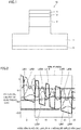
- Fig. 1 is a sectional view of a QCL 10 according to a first embodiment of the present invention.
- the QCL 10 includes a substrate 11 serving as a first contact layer, an active layer 12 disposed on an upper surface of the substrate 11, a second contact layer 13 disposed on an upper surface of the active layer 12, an upper electrode (second electrode) 14 in contact with an upper surface of the second contact layer 13, and a lower electrode (first electrode) 15 in contact with a lower surface of the substrate 11.
- the active layer 12 includes two or more active layer units stacked on top of each other.
- Each of the active layer units includes one or more quantum well layers and one or more barrier layers, and each of the quantum well layers and each of the barrier layers are alternately stacked.
- a part of the substrate 11 on the upper surface side, the active layer 12, and the second contact layer 13 are etched so that the QCL 10 has a mesa shape with a width of, for example, 10 ⁇ m.
- a waveguide is formed.
- the width of the waveguide may be changed in accordance with the use of the QCL 10.
- the width "10 ⁇ m" is merely an example of the width of a waveguide that allows single-mode oscillation of electromagnetic waves in the terahertz range.
- the substrate 11 is made of a compound semiconductor (first compound semiconductor).
- the first compound semiconductor is preferably represented by general formula Al x1 In y1 Ga (1-x1-y1) N (0 ⁇ x1 ⁇ 1, (0 ⁇ y1 ⁇ 1). More preferably, the first compound semiconductor is a material having a lattice constant close to that of a material used for quantum well layers described later. That is, the first compound semiconductor is GaN, InN, a fourth compound semiconductor described later, or a material having a lattice constant that is between the lattice constant of GaN or InN and the lattice constant of the fourth compound semiconductor.
- the substrate 11 is, for example, preferably an m-plane free-standing GaN substrate. More preferably, the substrate 11 is an m-plane free-standing GaN substrate polished after being cut so that the upper surface of the substrate has a (1-100) orientation. Thus, an AlGaN/GaN-based MQW structure having good crystal quality can be grown.
- the substrate 11 may be an m-plane free-standing GaN substrate polished after being cut so that the upper surface of the substrate has an off-angle of ⁇ 1° with respect to a (1-100) orientation. Also in this case, the present inventors have confirmed that an AlGaN/GaN-based MQW structure having good crystal quality can be grown.
- the substrate 11 may be an m-plane free-standing InN substrate. More preferably, the substrate 11 is an m-plane free-standing InN substrate polished after being cut so that the upper surface of the substrate has a (1-100) orientation. Thus, an InGaN/InN-based MQW structure having good crystal quality can be grown.
- the substrate 11 may be an m-plane free-standing InN substrate polished after being cut so that the upper surface of the substrate has an off-angle of ⁇ 1° with respect to a (1-100) orientation. Also in this case, the present inventors have confirmed that an InGaN/InN-based MQW structure having good crystal quality can be grown.
- the substrate 11 preferably contains an n-type dopant (e.g., Si). This decreases the resistance of the substrate 11 itself and also the contact resistance between the substrate 11 and the lower electrode 15.
- the n-type dopant concentration in the substrate 11 is preferably 1 ⁇ 10 17 /cm 3 or more and 5 ⁇ 10 19 /cm 3 or less and more preferably 1 ⁇ 10 17 /cm 3 or more and 3 ⁇ 10 18 /cm 3 or less.
- the thickness of the substrate 11 (the distance from the contact surface between the substrate 11 and the lower electrode 15 to the contact surface between the substrate 11 and the active layer 12) is preferably 0.1 ⁇ m or more and 500 ⁇ m or less and more preferably 0.1 ⁇ m or more and 50 ⁇ m or less.
- the quantum well layer of the active layer 12 is made of a compound semiconductor (third compound semiconductor).
- the vibrational energy of LO phonons of the third compound semiconductor is higher than the vibrational energy of LO phonons of GaAs and lower than or equal to the vibrational energy of LO phonons of AlN.
- the vibrational energy of LO phonons of the third compound semiconductor is higher than the vibrational energy of LO phonons of GaAs
- the difference in energy between carriers thermally excited to a level higher than the bottom of the energy band of the upper lasing level and the lower lasing level is smaller than the vibrational energy of LO phonons of the third compound semiconductor.
- Such a third compound semiconductor is preferably represented by general formula Al x3 In y3 Ga (1-x3-y3) N (0 ⁇ x3 ⁇ 1, 0 ⁇ y3 ⁇ 1).
- the third compound semiconductor is more preferably GaN or Al x3 In y3 Ga (1-x3-y3) N with at least one of x3 and y3 being controlled so as to provide a lattice constant close to the lattice constant of the first compound semiconductor, which is a material for the substrate 11.
- the substrate 11 is a GaN substrate such as an m-plane free-standing GaN substrate
- the third compound semiconductor is preferably GaN. This improves the crystal quality of the quantum well layer made of GaN.
- the third compound semiconductor is preferably InN. This improves the crystal quality of the quantum well layer made of InN.
- the thickness of the quantum well layer is preferably 1 nm or more and 100 nm or less and more preferably 1 nm or more and 6.5 nm or less. Thus, optical gain due to intersubband transition can be obtained.
- the quantum well layers of each of the active layer units may have the same thickness or different thicknesses.
- the thickness of the quantum well layer constituting the upper lasing level is preferably 1 nm or more and 7 nm or less and more preferably 1.5 nm or more and 3.5 nm or less.
- the thickness of the quantum well layer constituting the lower lasing level is preferably 1 nm or more and 7 nm or less and more preferably 1.5 nm or more and 3.5 nm or less.
- the thickness of the quantum well layer constituting the carrier-extraction level is preferably 1 nm or more and 20 nm or less and more preferably 4 nm or more and 12 nm or less.
- the main surface of the quantum well layer (the surface of the quantum well layer on which the barrier layer is formed) preferably has an orientation different from a (0001) orientation.
- a low internal electric field can be achieved in the QCL 10 compared with the case where the main surface of the quantum well layer has a (0001) orientation.
- the main surface of the quantum well layer has a (1-100) orientation.
- the internal electric field is decreased to a negligible degree in the QCL 10, and the crystal growth is easily performed.
- the present inventors have confirmed that even when the main surface of the quantum well layer has an off-angle of ⁇ 1° with respect to a (1-100) orientation, the internal electric field can be decreased to a negligible degree in the QCL 10, and the crystal growth is easily performed.
- the barrier layer of the active layer 12 is made of a compound semiconductor (fourth compound semiconductor).
- the vibrational energy of LO phonons of the fourth compound semiconductor is higher than the vibrational energy of LO phonons of GaAs and lower than or equal to the vibrational energy of LO phonons of AlN.
- the vibrational energy of LO phonons of the fourth compound semiconductor is higher than the vibrational energy of LO phonons of GaAs, even if carriers thermally excited to a level higher than the bottom of the energy band of the upper lasing level leak out to the barrier layer, the carriers can be prevented from losing energy as a result of LO phonon scattering. Thus, even when the QCL 10 is operated at room temperature, nonradiative transition can be effectively prevented.
- Such a fourth compound semiconductor is preferably represented by general formula Al x4 In y4 Ga (1-x4-y4) N (0 ⁇ x4 ⁇ 1, 0 ⁇ y4 ⁇ 1).
- the fourth compound semiconductor also preferably has a band gap energy higher than that of the third compound semiconductor constituting the quantum well layer. Accordingly, when the third compound semiconductor is GaN, the fourth compound semiconductor is preferably AlGaN. When the third compound semiconductor is InN, the fourth compound semiconductor is preferably InGaN. When the third compound semiconductor is Al x3 Ga (1-x3) N (0 ⁇ x3 ⁇ 1), the fourth compound semiconductor is preferably AlN.
- the thickness of the barrier layer is preferably 1 nm or more and 10 nm or less and more preferably 1.8 nm or more and 6.5 nm or less. This provides optical gain due to intersubband transition.
- At least one of the barrier layers preferably has a thickness of 1.8 nm or more. This prevents nonradiative transition of carriers to a different level due to elastic scattering (e.g., impurity scattering or roughness scattering). Therefore, the lasing at room temperature can be further stabilized. More preferably, all the barrier layers included in the active layer 12 have a thickness of 1.8 nm or more. This further prevents nonradiative transition of carriers to a different level due to elastic scattering, and thus the lasing at room temperature can be further stabilized.
- elastic scattering e.g., impurity scattering or roughness scattering
- the barrier layer having a thickness of 1.8 nm or more is disposed between the quantum well layer constituting the upper lasing level and the quantum well layer constituting the lower lasing level. This decreases the overlap between the wave function of the upper lasing level and the wave function of the lower lasing level ( Fig. 2 below). Therefore, the nonradiative transition (nonradiative transition due to elastic scattering such as impurity scattering or roughness scattering) from the upper lasing level to the lower lasing level can be prevented.
- an excessive decrease in the overlap between the wave function of the upper lasing level and the wave function of the lower lasing level because of the large thickness of the barrier layer makes it difficult to efficiently cause stimulated emission.
- the thickness of the barrier layer needs to be controlled to an appropriate thickness.
- the lasing at room temperature can be further stabilized.
- a barrier layer having a thickness of 1.8 nm or more and 3.0 nm or less is disposed between the quantum well layer constituting the upper lasing level and the quantum well layer constituting the lower lasing level.
- All the barrier layers included in the active layer 12 preferably have a thickness of 6.5 nm or less. This prevents an excessive increase in the thickness of each active layer unit, and thus lasing can be caused at a low threshold value.
- the barrier layers may have the same thickness or different thicknesses.
- the main surface of the barrier layer (the surface of the barrier layer on which the quantum well layer is formed) preferably has an orientation different from a (0001) orientation. This suppresses the internal electric field in the QCL 10 compared with the case where the main surface of the barrier layer has a (0001) orientation. Thus, the QCL 10 is easily designed. Furthermore, even if a plurality of barrier layers included in the active layer 12 have different thicknesses or compositions, the performance of the QCL 10 can be prevented from degrading.
- the main surface of the barrier layer has a (1-100) orientation.
- the internal electric field is decreased to a negligible degree in the QCL 10, and the crystal growth is easily performed.
- the present inventors have confirmed that even when the main surface of the barrier layer has an off-angle of ⁇ 1° with respect to a (1-100) orientation, the internal electric field can be decreased to a negligible degree in the QCL 10, and the crystal growth is easily performed.
- the number of active layer units in the active layer 12 is not particularly limited.
- the number of the quantum well layers and the number of the barrier layers in each of the active layer units are not particularly limited.
- Each of the active layer units preferably includes three or more of the quantum well layers and three or more of the barrier layers. This suppresses a decrease in the resistance at a lasing threshold value or lower, which stably causes lasing.
- each of the active layer units includes three of the quantum well layers and three of the barrier layers. This stably causes lasing. Furthermore, a large region where optical gain is generated can be ensured in each of the active layer units, and thus lasing can be caused at a low threshold value.
- the generation of the above-described resonant state can be sometimes prevented until the bias voltage increases to a bias voltage at which the maximum optical gain is maximized (refer to Fig. 4 described below).
- the lasing can be further stabilized at room temperature.
- the optical gain is sometimes present in the above-described resonant state (refer to Fig. 6 described below).
- the lasing can be further stabilized at room temperature.
- the thickness of the active layer 12 is preferably 0.5 ⁇ m or more and 100 ⁇ m or less and more preferably 1 ⁇ m or more and 20 ⁇ m or less.
- the second contact layer 13 is made of a compound semiconductor (second compound semiconductor).
- the second compound semiconductor is preferably represented by general formula Al x2 ln y2 Ga (1-x2-y2) N (0 ⁇ x2 ⁇ 1, (0 ⁇ y2 ⁇ 1). More preferably, the second compound semiconductor is a material having a lattice constant close to that of a material used for the above-described quantum well layer. That is, the second compound semiconductor is GaN, InN, the above-described fourth compound semiconductor, or a material having a lattice constant that is between the lattice constant of GaN or InN and the lattice constant of the fourth compound semiconductor.
- the second contact layer 13 preferably contains an n-type dopant (e.g., Si). This decreases the resistance of the second contact layer 13 itself and also the contact resistance between the second contact layer 13 and the upper electrode 14.
- the n-type dopant concentration in the second contact layer 13 is preferably 1 ⁇ 10 17 /cm 3 or more and 1 ⁇ 10 20 /cm 3 or less and more preferably 1 ⁇ 10 18 /cm 3 or more and 5 ⁇ 10 19 /cm 3 or less.
- the thickness of the second contact layer 13 is preferably 0.05 ⁇ m or more and 3 ⁇ m or less and more preferably 0.1 ⁇ m or more and 1 ⁇ m or less.
- the upper electrode 14 is preferably made of a metal material having good ohmic characteristics with the second contact layer 13.
- the upper electrode 14 is, for example, an ohmic electrode including Ti layers and Al layers stacked on top of each other.
- the upper electrode 14 may be made of a metal different from Ti and Al or may be a transparent oxide electrode.
- the lower electrode 15 is preferably made of a metal material having good ohmic characteristics with the substrate 11.
- the lower electrode 15 is, for example, an ohmic electrode including Ti layers and Al layers stacked on top of each other.
- the lower electrode 15 may be made of a metal different from Ti and Al or may be a transparent oxide electrode.
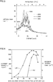
- the horizontal axis shows a position in the active layer in a thickness direction and the vertical axis shows the potential energy of electrons.
- "One period" enclosed in a dotted line corresponds to a single active layer unit.
- L201 to L208 show energy levels (calculated results). In each of L201 to L208, the value on the vertical axis is the potential energy of electrons and the shape corresponds to a shape of the wave function. Furthermore, L210 shows an energy band structure (calculated results) of the active layer.
- the one-period active layer unit includes three quantum well layers and three barrier layers, and each of the quantum well layers and each of the barrier layers are alternately stacked.
- the composition and thickness of each of the quantum well layers and the composition and thickness of each of the barrier layers were as follows.
- the "first layer” described later is a leftmost layer in the region enclosed in a dotted line in Fig. 2 .
- the "sixth layer” described later is a rightmost layer in the region enclosed in a dotted line in Fig. 2 and contains Si in a concentration of 3 ⁇ 10 17 /cm 3 in order to generate electrons.
- the active layer unit included in the region enclosed in a dotted line formed the energy levels L203 to L208.
- the energy levels L203 and L204 are upper lasing levels
- the energy levels L205 and L206 are lower lasing levels
- the energy levels L207 and L208 are carrier-extraction levels.
- the energy levels L201 and L202 are carrier-extraction levels in an active layer unit located on the left side of the active layer unit included in the region enclosed in a dotted line in Fig. 2 .
- the carriers When carriers are injected into the energy levels L203 and L204 from the active layer unit located on the left side of the active layer unit included in the region enclosed in a dotted line in Fig. 2 , the carriers are subjected to stimulated emission from the energy levels L203 and L204 toward the energy levels L205 and L206 (radiative transition). Then, the carriers reach the sixth layer (quantum well layer) by tunneling and are scattered by LO phonons (the vibrational energy of LO phonons of GaN is 92 meV) to cause transition to the energy levels L207 and L208.
- the carriers subjected to the transition to the energy levels L207 and L208 are injected into an active layer unit located on the right side of the active layer unit included in the region enclosed in a dotted line in Fig. 2 .
- the above-described processes are repeatedly conducted.
- the second layer forms the upper lasing level and the fourth layer forms the lower lasing level.
- the third layer located between the second layer and the fourth layer has a thickness of 2.0 mm. This suppresses the nonradiative transition from the upper lasing level to the lower lasing level due to elastic scattering such as impurity scattering or roughness scattering. It has been found from the calculation conducted by the present inventors that such an effect is considerably produced when the barrier layer disposed between the quantum well layer that forms the upper lasing level and the quantum well layer that forms the lower lasing level has a thickness of 1.8 nm or more.
- a thickness of 1.8 nm or more of the barrier layer sharply weakens the bond between the quantum well layer that forms the upper lasing level and the quantum well layer that forms the lower lasing level. In other words, the overlap between the wave function of the upper lasing level and the wave function of the lower lasing level decreases ( Fig. 2 ).
- Fig. 3 illustrates the optical gain obtained when a bias voltage of about 95 meV per active layer unit was applied, the optical gain being calculated by a nonequilibrium Green's function method. It is clear from the results that even when a QCL including the above-described active layer units is operated at 300 K, optical gain is obtained in a wide frequency range of 2.5 to 6 THz. In particular, in a frequency range of 3.2 to 4.8 THz, the optical gain exceeds 10 cm -1 and the maximum optical gain is about 15 cm -1 . Thus, it has been found that the QCL including the above-described active layer units has optical gain sufficient for lasing at room temperature.
- Fig. 4 illustrates the relationship (calculation results) between the bias voltage applied per active layer unit and the current density J and maximum optical gain when a QCL including the above-described active layer units was operated at 300 K.
- L401 shows the relationship between the bias voltage and the current density J
- L402 shows the relationship between the bias voltage and the maximum optical gain.
- a decrease in the current density J has not been confirmed until the bias voltage increases to a value (about 95 meV) at which the maximum optical gain is maximized.
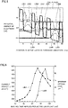
- the horizontal axis shows a position in the active layer in a thickness direction and the vertical axis shows the potential energy of electrons.
- "One period" enclosed in a dotted line corresponds to a single active layer unit.
- L501 to L508 show energy levels (calculated results). In each of L501 to L508, the value on the vertical axis is the potential energy of electrons and the shape corresponds to a shape of the wave function. Furthermore, L510 shows an energy band structure (calculated results) of the active layer.
- each of the quantum well layers and the composition and thickness of each of the barrier layers were as follows.
- the "first layer” described later is a leftmost layer in the region enclosed in a dotted line in Fig. 5 .
- the "sixth layer” described later is a rightmost layer in the region enclosed in a dotted line in Fig. 5 and contains Si in a concentration of 3 ⁇ 10 17 /cm 3 in order to generate electrons.
- the active layer unit included in the region enclosed in a dotted line formed the energy levels L503 to L508.
- the energy levels L503 and L504 are upper lasing levels
- the energy levels L505 and L506 are lower lasing levels
- the energy levels L507 and L508 are carrier-extraction levels.
- the energy levels L501 and L502 are carrier-extraction levels in an active layer unit located on the left side of the active layer unit included in the region enclosed in a dotted line in Fig. 5 .
- the carriers When carriers are injected into the energy levels L503 and L504 from the active layer unit located on the left side of the active layer unit included in the region enclosed in a dotted line in Fig. 5 , the carriers are subjected to stimulated emission from the energy levels L503 and L504 toward the energy levels L505 and L506 (radiative transition). Then, the carriers reach the sixth layer (quantum well layer) by tunneling and are scattered by LO phonons (the vibrational energy of LO phonons of InN is 72.6 meV) to cause transition to the energy levels L507 and L508.
- the sixth layer quantum well layer
- the carriers subjected to the transition to the energy levels L507 and L508 are injected into an active layer unit located on the right side of the active layer unit included in the region enclosed in a dotted line in Fig. 5 .
- the above-described processes are repeatedly conducted.
- the second layer forms the upper lasing level and the fourth layer forms the lower lasing level.
- the third layer located between the second layer and the fourth layer has a thickness of 4.0 mm. Therefore, the overlap between the wave function of the upper lasing level and the wave function of the lower lasing level is believed to be considerably small. This suppresses the nonradiative transition from the upper lasing level to the lower lasing level due to elastic scattering such as impurity scattering or roughness scattering.
- the optical gain obtained when a bias voltage of about 80 meV per active layer unit is applied is calculated by a nonequilibrium Green's function method. It has been found that the optical gain is maximized (20 cm -1 ) at a frequency of about 3 THz.
- Fig. 6 illustrates the relationship (calculation results) between the bias voltage applied per active layer unit and the current density J and maximum optical gain when a QCL including the above-described active layer units was operated at 300 K.
- L601 shows the relationship between the bias voltage and the current density J
- L602 shows the relationship between the bias voltage and the maximum optical gain.
- a decrease in the current density J has been confirmed at a bias voltage of about 73 meV, which is a bias voltage just before a bias voltage (about 90 meV) at which the maximum optical gain is maximized. Therefore, if a bias voltage of about 90 meV per active layer unit is applied, lasing may become unstable. However, even when a bias voltage of about 73 meV per active layer unit is applied, optical gain is still present. Accordingly, it is believed that lasing can be caused by applying a bias voltage of about 73 meV per active layer unit even at room temperature.
- an active layer 12 and a second contact layer 13 are formed on an upper surface of a substrate 11 by, for example, a molecular beam epitaxy (MBE) method or a metal organic vapor phase epitaxy (MOVPE) method.
- MBE molecular beam epitaxy
- MOVPE metal organic vapor phase epitaxy
- an upper electrode 14 is formed on an upper surface of the second contact layer 13 and a lower electrode 15 is formed on a lower surface of the substrate 11 by, for example, an electron-beam deposition method.
- the upper electrode 14, the second contact layer 13, the active layer 12, and a part of the substrate 11 are etched by, for example, a reactive ion etching (RIE) method to form a mesa shape illustrated in Fig. 1 .
- RIE reactive ion etching
- Fig. 7 is a sectional view of a QCL 20 according to a second embodiment of the present invention.
- a supporting substrate 21 is disposed on an upper surface of an upper electrode 14.
- points different from those in the first embodiment will be mainly described.
- the supporting substrate 21 is bonded to the upper electrode 14 or is electrically connected to the upper electrode 14.
- the thickness of the substrate 11 can be decreased.
- the thickness of the substrate 11 can be decreased to 10 ⁇ m or less. Since the distance between the upper electrode 14 and the lower electrode 15 is decreased, the ratio of a region where optical gain is generated in the active layer unit can be increased. Thus, highly efficient lasing can be achieved. For example, lasing can be caused at a low threshold value.
- the QCL 20 can be produced by the following method. First, the upper electrode 14 is formed by the method described in the first embodiment. Then, a supporting substrate 21 is fixed onto an upper surface of the upper electrode 14 using solder such as AuSn. Subsequently, the lower surface of the substrate 11 is polished until the substrate thickness reaches 10 ⁇ m or less. Instead of the polishing of the lower surface of the substrate 11, the thickness of the substrate 11 may be decreased by laser lift-off, chemical etching, or the like. Subsequently, the upper electrode 14, the second contact layer 13, the active layer 12, and the substrate 11 are etched from the lower surface side of the substrate 11 by, for example, an RIE method. A lower electrode 15 is then formed on the lower surface of the substrate 11.
- Fig. 8 is a sectional view of a QCL 30 according to a third embodiment of the present invention. Hereafter, points different from those in the first embodiment will be mainly described.
- a metal layer 31 is disposed between the upper electrode 14 and the lower electrode 15. This increases the confinement factor of electromagnetic waves, which allows lasing at a low threshold value.
- Electromagnetic waves in the terahertz range have a wavelength of several tens of micrometers to several hundred micrometers.
- the thickness of the active layer 12 having optical gain required for lasing is several micrometers to ten micrometers, and electromagnetic waves need to be confined in the active layer 12 in order to efficiently cause lasing. If the metal layer 31 is disposed between the upper electrode 14 and the lower electrode 15, electromagnetic waves in the terahertz range can be confined between the metal layer 31 and the upper electrode 14 with more certainty. Consequently, the overlap of electromagnetic waves and the active layer 12 can be increased compared with the QCL 10, that is, the confinement factor of electromagnetic waves is increased. Thus, lasing can be caused at a low threshold value.
- the metal layer 31 is disposed inside a first contact layer 32.
- the metal layer 31 that produces the above effect can be easily formed.
- the metal layer 31 may be disposed inside the second contact layer 13.
- electromagnetic waves in the terahertz range can be confined between the metal layer 31 and the lower electrode 15 with more certainty. Consequently, the overlap of electromagnetic waves and the active layer 12 can be increased compared with the QCL 10, that is, the confinement factor of electromagnetic waves is increased. Thus, lasing can be caused at a low threshold value, and the metal layer 31 can be easily formed.
- the material for the metal layer 31 is preferably a metal (metal with high thermal resistance), such as tungsten (W) or copper (Cu), that is not altered at a growth temperature at which compound semiconductor layers such as the active layer 12 and the second contact layer 13 are subjected to crystal growth.
- a metal metal with high thermal resistance
- W tungsten
- Cu copper
- the thickness of the metal layer 31 is preferably 0.01 ⁇ m or more and 1 ⁇ m or less and more preferably 0.03 ⁇ m or more and 0.2 ⁇ m or less.
- the first contact layer 32 preferably has the same composition as the second contact layer 13, preferably contains an n-type dopant in the same concentration as that of the second contact layer 13, and preferably has the same thickness as the second contact layer 13.
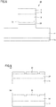
- Figs. 9(a) and 9(b) are sectional views partly illustrating a method for producing the QCL 30 in the order of processes.
- a first contact layer 32 is formed on an upper surface of a substrate 11, and then a metal layer is formed on the entire upper surface of the first contact layer 32 by, for example, a sputtering method.
- the metal layer is patterned by photolithography to form a striped metal layer 31 ( Fig. 9(a) ).
- the stripe formed preferably extends in a direction parallel to a (0001) orientation of a compound semiconductor constituting the first contact layer 32 or in a direction perpendicular to the (0001) orientation.
- the width of openings formed by patterning the metal layer is preferably about 1 ⁇ m, and the width of the metal layer 31 is preferably about 20 ⁇ m.
- the first contact layer 32 is then regrown.
- the first contact layer 32 grows in a transverse direction, and consequently the metal layer 31 is buried in the first contact layer 32 ( Fig. 9(b) ).
- the active layer 12, the second contact layer 13, the upper electrode 14, and the lower electrode 15 are formed by the method described in the first embodiment.
- a QCL 30 is produced.
- the following technique has been widely known.
- selective growth in a transverse direction is promoted using a mask made of a metal or an insulator to form a high-quality thin film.
- the mask is formed inside a layer disposed on at least one layer which is different from the active layer and is disposed on the active layer.
- the substrate 11 When a free-standing substrate is used as the substrate 11, the substrate 11 is formed of a high-quality crystal. Therefore, if selective growth in a transverse direction is promoted using the known mask, a conductivity type dopant is accidentally doped into the growth layer or formation of crystal defects is facilitated in the growth layer.
- the metal layer 31 is disposed in a layer (the first contact layer 32 in this embodiment) that is in contact with the active layer 12 in order to increase the confinement factor of electromagnetic waves. Therefore, the configuration of the metal layer 31 is different from that of the above-described mask.
- the first contact layer 32 is grown in a transverse direction using the metal layer 31 as a mask, a conductivity type dopant can be prevented from being accidentally doped into the first contact layer 32, and the facilitated formation of crystal defects in the first contact layer 32 can be prevented.
- Fig. 10 is a sectional view of a QCL 40 according to a fourth embodiment of the present invention.
- points different from those in the third embodiment will be mainly described.
- the metal layer 31 is disposed on the substrate 11 with the first contact layer 32 sandwiched therebetween. Since the metal layer 31 is electrically connected to the first contact layer 32, a voltage can be directly applied to the metal layer 31. That is, the metal layer 31 can be used as the lower electrode 15 in the first to third embodiments.
- the first contact layer 32 is formed by selective growth using the metal layer 31 as a mask. Therefore, the metal layer 31 functions as a layer for selectively growing the first contact layer 32, functions as a layer for increasing the confinement factor of electromagnetic waves, and functions as a substitute for the lower electrode 15. Thus, the metal layer 31 and the first contact layer 32 can be easily formed.
- the substrate 11 may have an orientation (e.g., a plane ((11-20) orientation)) different from the m plane.
- the substrate 11 may be a composite substrate obtained by forming an m-plane free-standing GaN layer or an m-plane free-standing InN layer on an upper surface of a sapphire substrate or a SiC substrate.
- GaAs-based materials and GaN-based materials which have been used as materials for QCLs, have considerably different physical properties and characteristics. Therefore, when a QCL is produced using a GaN-based material, the QCL needs to be produced under a design guideline different from before.
- the effective mass of GaN-based materials is large, and thus the broadening of energy levels is much larger in GaN-based materials than in GaAs-based materials. Therefore, if a QCL containing a GaN-based material is produced under the same design guideline as that for producing a QCL using a GaAs-based material, problems occur such as unstable operation of the QCL and impossibility of causing lasing in the QCL.
- the QCL containing a GaN-based material can be stably operated.
- the QCL 10 illustrated in Fig. 1 or the like includes a first electrode 15, a first contact layer 11 that is in contact with the first electrode 15 and is made of a first compound semiconductor, a second electrode 14 having a polarity opposite to that of the first electrode 15, a second contact layer 13 that is in contact with the second electrode 14 and is made of a second compound semiconductor, and an active layer 12 disposed between the first contact layer 11 and the second contact layer 13 and including two or more active layer units.
- Each of the active layer units includes one or more quantum well layers made of a third compound semiconductor and one or more barrier layers made of a fourth compound semiconductor, and each of the quantum well layers and each of the barrier layers are alternately stacked.
- the vibrational energies of longitudinal optical phonons of the third compound semiconductor and the fourth compound semiconductor are higher than the vibrational energy of a longitudinal optical phonon of GaAs and lower than or equal to the vibrational energy of a longitudinal optical phonon of AlN.
- lasing can be stably caused at room temperature.
- the third compound semiconductor is preferably Al x3 lny 3 Ga (1-x3-y3) N (0 ⁇ x3 ⁇ 1, (0 ⁇ y3 ⁇ 1)
- the fourth compound semiconductor is preferably Al x4 In y4 Ga (1-x4-y4) N (0 ⁇ x4 ⁇ 1, 0 ⁇ y4 ⁇ 1).
- the fourth compound semiconductor preferably has a band gap energy higher than that of the third compound semiconductor. Thus, crystal growth of the quantum well layer and the barrier layer is easily performed.
- At least one of the barrier layers preferably has a thickness of 1.8 nm or more. This prevents nonradiative transition of carriers to a different level by elastic scattering.
- the barrier layer having a thickness of 1.8 nm or more is disposed between a quantum well layer constituting an upper lasing level and a quantum well layer constituting a lower lasing level. This decreases the overlap between the wave function of the upper lasing level and the wave function of the lower lasing level.
- all the barrier layers included in the active layer 12 have a thickness of 1.8 nm or more. This further prevents nonradiative transition of carriers to a different level by elastic scattering.
- All the barrier layers included in the active layer 12 preferably have a thickness of 6.5 nm or less. This prevents an excessive increase in the thickness of the active layer units.
- Each of the active layer units preferably includes three or more of the quantum well layers and three or more of the barrier layers. This suppresses a decrease in the resistance at a lasing threshold value or lower.
- each of the active layer units includes three of the quantum well layers and three of the barrier layers. This provides a large region where optical gain is generated in each of the active layer units.
- the main surface of each of the quantum well layers and the main surface of each of the barrier layers have an orientation different from a (0001) orientation. This decreases the internal electric field.
- the main surface of each of the quantum well layers and the main surface of each of the barrier layers have an off-angle of ⁇ 1° with respect to a (1-100) orientation. This decreases the internal electric field to a negligible degree.
- a supporting substrate 21 bonded to the first electrode 15 or the second electrode 14 or a supporting substrate 21 electrically connected to the first electrode 15 or the second electrode 14 is preferably further included. This allows lasing at a low threshold value.
- a metal layer 31 is preferably disposed between the first electrode 15 and the second electrode 14. This increases the confinement factor of electromagnetic waves. More preferably, the metal layer 31 is disposed in at least one of the first contact layer 32 and the second contact layer 13.
- At least one of the first contact layer 32 and the second contact layer 13 is preferably formed by selective growth using the metal layer 31 as a mask. This makes it easy to form the first contact layer 32 or the second contact layer 13 and the metal layer 31.
Landscapes
- Physics & Mathematics (AREA)
- Condensed Matter Physics & Semiconductors (AREA)
- General Physics & Mathematics (AREA)
- Electromagnetism (AREA)
- Optics & Photonics (AREA)
- Semiconductor Lasers (AREA)
Abstract
Description
- The present invention relates to a quantum cascade laser.
- Quantum cascade lasers (hereafter referred to as "QCLs") are promising light sources capable of generating electromagnetic waves from the infrared range to the terahertz range (300 GHz to 10 THz) with high power, and the research and development of such quantum cascade lasers has been accelerated in recent years. In particular, there are no promising light sources (small light sources formed of a compound semiconductor) capable of generating electromagnetic waves in the terahertz range, except for QCLs. Therefore, QCLs are the most promising light sources capable of generating electromagnetic waves in the terahertz range. In such QCLs, intersubband population inversion in the conduction band or intersubband population inversion in the valence band in a multiple quantum well (hereafter referred to as "MQW") structure formed of a compound semiconductor occurs, which causes lasing.
- QCLs capable of generating electromagnetic waves in the terahertz range have been often produced using a GaAs-based material, an InP-based material, or a GaSb-based material. However, lasing at a temperature of 200 K or higher has not been reported with any of the materials.
- The factor of inhibiting lasing at a temperature of 200 K or higher is thermally excited phonon scattering. The thermally excited phonon scattering refers to a phenomenon in which when electrons or holes (hereafter referred to as "carriers") at the upper lasing level obtain in-plane kinetic energy by heat and thus the difference in energy between the carriers and the lower lasing level is higher than or equal to the vibrational energy of longitudinal optical (hereafter referred to as "LO") phonons, the carriers are scattered by the LO phonons to cause nonradiative relaxation to the lower lasing level.
- For example, in a QCL (including a GaAs layer as a quantum well layer) that generates electromagnetic waves with about 2 THz (about 9 meV), the energy difference between the upper lasing level and the lower lasing level is about 9 meV (energy corresponding to lasing wavelength). At low temperatures, carriers are often present at the bottom of the energy band of the upper lasing level. Therefore, the transition of carriers present at the upper lasing level to the lower lasing level by LO phonon scattering does not occur.
- However, when the temperature increases, carriers are thermally excited and the distribution becomes similar to, for example, a quasi-Fermi distribution. When the difference in energy between carriers thermally excited to the level higher than the bottom of the energy band of the upper lasing level and the lower lasing level is concordant with the vibrational energy of LO phonons of a compound semiconductor constituting the quantum well layer of the QCL, the thermally excited carriers are subjected to transition to the lower lasing level by LO phonon scattering. This transition occurs with higher probability than the stimulated emission from the upper lasing level to the lower lasing level. That is, the thermally excited carriers lose energy by not generation of electromagnetic waves but by LO phonon scattering. In addition, if the thermally excited carriers are subjected to transition to the lower lasing level by LO phonon scattering, the carriers that have lost energy occupy the lower lasing level, which suppresses the occurrence of population inversion. As a result, lasing is suppressed.
- For example, in the above-described QCL, when carriers present at the upper lasing level obtain an energy of about 27 meV by heat, LO phonon scattering (nonradiative transition) becomes dominant, which suppresses lasing. Herein, the vibrational energy of LO phonons is a physical property intrinsic to materials. Therefore, if a GaAs layer is used as a quantum well layer in a QCL capable of generating electromagnetic waves in the terahertz range, it is difficult to operate the QCL at room temperature.
- It is proposed in
PTL 1 that a layer made of a compound semiconductor different from GaAs is used as a quantum well layer in a QCL capable of generating electromagnetic waves in the terahertz range.PTL 1 discloses that a GaN layer is used as a quantum well layer, and the vibrational energy of LO phonons of GaN is about 90 meV. Therefore, the occurrence of the above-described thermally excited phonon scattering is believed to be prevented. - PTL 1: Japanese Unexamined Patent Application Publication No.
2013-171842 -
Fig. 11 illustrates a spectral function of a GaN-based THz-QCL disclosed inPTL 1. In this GaN-based THz-QCL, an AlGaN/GaN-based MQW structure is formed on an upper surface of a c-plane GaN layer.Fig. 11 illustrates a spectral function in a state in which a bias voltage is applied to a degree that lasing can be caused. The "1 unit " illustrated inFig. 11 includes two quantum well layers. In the state in which a bias voltage is applied to a degree that lasing can be caused, the energy level (3) of the quantum well layer on the left side is higher than the energy level (2) of the quantum well layer on the right side (Fig. 11 ). However, the quantum well width of the quantum well layer on the right side is smaller than the quantum well width of the quantum well layer on the left side, and thus the quantum well layer on the right side has a larger quantum confinement effect than the quantum well layer on the left side. In a state in which the bias voltage is not applied, therefore, the energy level (2) of the quantum well layer on the right side is higher than the energy level (3) of the quantum well layer on the left side. In other words, during the change in the state from no application of bias voltage to application of bias voltage to a degree that lasing can be caused, there is a state (resonant state) in which the energy at the ground level of the quantum well layer on the left side is substantially equal to the energy at the ground level of the quantum well layer on the right side. - In the resonant state, the movement of carriers between the quantum well layer on the left side and the quantum well layer on the right side occurs because of tunneling, and therefore the resistance is substantially decreased. That is, in a state in which the bias voltage is slightly lower than that in the resonant state and in a state in which the bias voltage is slightly higher than that in the resonant state, the resistance is higher than that in the resonant state. Therefore, if the resonant state is generated while a bias voltage lower than the bias voltage required for lasing is applied, the operation of a laser becomes unstable. Thus, it can be expected that the operation of the QCL disclosed in
PTL 1 tends to become unstable. -
PTL 1 does not disclose any restriction concerning the configuration of a barrier layer. Since QCLs are operated by tunneling of carriers through a barrier layer, the configuration of a barrier layer is as important as the configuration of a quantum well layer. If the configuration of a barrier layer is not appropriately selected, carriers that have leaked out to the barrier layer are subjected to nonradiative relaxation by LO phonon scattering between the upper lasing level and the lower lasing level, which sometimes suppresses lasing. - Accordingly, it is an object of the present invention to provide a QCL capable of stably causing lasing at room temperature.
- A quantum cascade laser according to the present invention includes a first electrode, a first contact layer that is in contact with the first electrode and is made of a first compound semiconductor, a second electrode having a polarity opposite to that of the first electrode, a second contact layer that is in contact with the second electrode and is made of a second compound semiconductor, and an active layer disposed between the first contact layer and the second contact layer and including two or more active layer units. Each of the active layer units includes one or more quantum well layers made of a third compound semiconductor and one or more barrier layers made of a fourth compound semiconductor, and each of the quantum well layers and each of the barrier layers are alternately stacked. The vibrational energies of longitudinal optical phonons of the third compound semiconductor and the fourth compound semiconductor are higher than the vibrational energy of a longitudinal optical phonon of GaAs and lower than or equal to the vibrational energy of a longitudinal optical phonon of AlN.
- The third compound semiconductor is preferably Alx3Iny3Ga(1-x3-y3)N (0 ≤ x3 ≤ 1, (0 ≤ y3 ≤ 1). The fourth compound semiconductor is preferably Alx4Iny4Ga(1-x4-y4)N (0 ≤ x4 ≤ 1, 0 ≤ y4 ≤ 1). The fourth compound semiconductor preferably has a band gap energy higher than that of the third compound semiconductor.
- At least one of the barrier layers preferably has a thickness of 1.8 nm or more. More preferably, the barrier layer having a thickness of 1.8 nm or more is disposed between a quantum well layer constituting an upper lasing level and a quantum well layer constituting a lower lasing level.
- All the barrier layers included in the active layer preferably have a thickness of 1.8 nm or more and 6.5 nm or less.
- Each of the active layer units preferably includes three or more of the quantum well layers and three or more of the barrier layers and more preferably includes three of the quantum well layers and three of the barrier layers.
- The main surface of each of the quantum well layers and the main surface of each of the barrier layers preferably have an orientation different from a (0001) orientation and more preferably have an off-angle of ±1° with respect to a (1-100) orientation.
- The quantum cascade laser preferably further includes a supporting substrate bonded to the first electrode or the second electrode or a supporting substrate electrically connected to the first electrode or the second electrode.
- A metal layer is preferably disposed between the first electrode and the second electrode. The metal layer is preferably disposed in at least one of the first contact layer and the second contact layer. At least one of the first contact layer and the second contact layer is preferably formed by selective growth using the metal layer as a mask.
- In the QCL according to the present invention, lasing can be stably caused at room temperature.
-
- [
Fig. 1] Fig. 1 is a sectional view of a QCL according to an embodiment of the present invention. - [
Fig. 2] Fig. 2 illustrates the energy band structure and the shape of a wave function of an active layer according to an embodiment of the present invention. - [
Fig. 3] Fig. 3 is a graph illustrating a gain spectrum of an active layer according to an embodiment of the present invention. - [
Fig. 4] Fig. 4 is a graph illustrating the relationship between a bias voltage applied per active layer unit according to an embodiment of the present invention and the current density J and maximum optical gain. - [
Fig. 5] Fig. 5 illustrates the energy band structure and the shape of a wave function of an active layer according to an embodiment of the present invention. - [
Fig. 6] Fig. 6 is a graph illustrating the relationship between a bias voltage applied per active layer unit according to an embodiment of the present invention and the current density J and maximum optical gain. - [
Fig. 7] Fig. 7 is a sectional view of a QCL according to an embodiment of the present invention. - [
Fig. 8] Fig. 8 is a sectional view of a QCL according to an embodiment of the present invention. - [
Fig. 9] Fig. 9 illustrates sectional views partly illustrating a method for producing a QCL according to an embodiment of the present invention in the order of processes. - [
Fig. 10] Fig. 10 is a sectional view of a QCL according to an embodiment of the present invention. - [
Fig. 11] Fig. 11 is a graph illustrating a spectral function of a QCL disclosed inPTL 1. - Hereafter, the present invention will be described with reference to the attached drawings. Although a QCL that generates electromagnetic waves in the terahertz range will be described below, a QCL of the present invention is not limited to the QCL that generates electromagnetic waves in the terahertz range. In the drawings of the present invention, the same reference numerals denote the same parts or the corresponding parts. The dimensions such as length, width, thickness, and depth are appropriately changed to clarify and simplify the drawings, and do not correspond to the actual dimensions.
-
Fig. 1 is a sectional view of aQCL 10 according to a first embodiment of the present invention. TheQCL 10 includes asubstrate 11 serving as a first contact layer, anactive layer 12 disposed on an upper surface of thesubstrate 11, asecond contact layer 13 disposed on an upper surface of theactive layer 12, an upper electrode (second electrode) 14 in contact with an upper surface of thesecond contact layer 13, and a lower electrode (first electrode) 15 in contact with a lower surface of thesubstrate 11. Theactive layer 12 includes two or more active layer units stacked on top of each other. Each of the active layer units includes one or more quantum well layers and one or more barrier layers, and each of the quantum well layers and each of the barrier layers are alternately stacked. - A part of the
substrate 11 on the upper surface side, theactive layer 12, and thesecond contact layer 13 are etched so that theQCL 10 has a mesa shape with a width of, for example, 10 µm. Thus, a waveguide is formed. The width of the waveguide may be changed in accordance with the use of theQCL 10. The width "10 µm" is merely an example of the width of a waveguide that allows single-mode oscillation of electromagnetic waves in the terahertz range. - The
substrate 11 is made of a compound semiconductor (first compound semiconductor). The first compound semiconductor is preferably represented by general formula Alx1Iny1Ga(1-x1-y1)N (0 ≤ x1 ≤ 1, (0 ≤ y1 ≤ 1). More preferably, the first compound semiconductor is a material having a lattice constant close to that of a material used for quantum well layers described later. That is, the first compound semiconductor is GaN, InN, a fourth compound semiconductor described later, or a material having a lattice constant that is between the lattice constant of GaN or InN and the lattice constant of the fourth compound semiconductor. - The
substrate 11 is, for example, preferably an m-plane free-standing GaN substrate. More preferably, thesubstrate 11 is an m-plane free-standing GaN substrate polished after being cut so that the upper surface of the substrate has a (1-100) orientation. Thus, an AlGaN/GaN-based MQW structure having good crystal quality can be grown. Thesubstrate 11 may be an m-plane free-standing GaN substrate polished after being cut so that the upper surface of the substrate has an off-angle of ±1° with respect to a (1-100) orientation. Also in this case, the present inventors have confirmed that an AlGaN/GaN-based MQW structure having good crystal quality can be grown. - The
substrate 11 may be an m-plane free-standing InN substrate. More preferably, thesubstrate 11 is an m-plane free-standing InN substrate polished after being cut so that the upper surface of the substrate has a (1-100) orientation. Thus, an InGaN/InN-based MQW structure having good crystal quality can be grown. Thesubstrate 11 may be an m-plane free-standing InN substrate polished after being cut so that the upper surface of the substrate has an off-angle of ±1° with respect to a (1-100) orientation. Also in this case, the present inventors have confirmed that an InGaN/InN-based MQW structure having good crystal quality can be grown. - The
substrate 11 preferably contains an n-type dopant (e.g., Si). This decreases the resistance of thesubstrate 11 itself and also the contact resistance between thesubstrate 11 and thelower electrode 15. The n-type dopant concentration in thesubstrate 11 is preferably 1 × 10¹⁷ /cm3 or more and 5 × 10¹⁹ /cm3 or less and more preferably 1 × 10¹⁷ /cm3 or more and 3 × 10¹⁸ /cm3 or less. - The thickness of the substrate 11 (the distance from the contact surface between the
substrate 11 and thelower electrode 15 to the contact surface between thesubstrate 11 and the active layer 12) is preferably 0.1 µm or more and 500 µm or less and more preferably 0.1 µm or more and 50 µm or less. - <Active layer>
- The quantum well layer of the
active layer 12 is made of a compound semiconductor (third compound semiconductor). The vibrational energy of LO phonons of the third compound semiconductor is higher than the vibrational energy of LO phonons of GaAs and lower than or equal to the vibrational energy of LO phonons of AlN. - When the vibrational energy of LO phonons of the third compound semiconductor is higher than the vibrational energy of LO phonons of GaAs, the difference in energy between carriers thermally excited to a level higher than the bottom of the energy band of the upper lasing level and the lower lasing level is smaller than the vibrational energy of LO phonons of the third compound semiconductor. This prevents the transition of thermally excited carriers to the lower lasing level by LO phonon scattering. That is, the thermally excited carriers can be prevented from losing energy as a result of LO phonon scattering. Thus, even when the
QCL 10 is operated at room temperature, nonradiative transition can be prevented. - Furthermore, if the transition of the thermally excited carriers to the lower lasing level by LO phonon scattering can be prevented, carriers that have lost energy can be prevented from occupying the lower lasing level. This facilitates formation of population inversion, which allows lasing. Accordingly, lasing can be stably caused even at room temperature in the QCL 10 (
Fig. 3 described later). - When the vibrational energy of LO phonons of the third compound semiconductor is lower than or equal to the vibrational energy of LO phonons of AlN, an excessive increase in scattering probability by LO phonons can be prevented, which suppresses energy broadening associated with the uncertainty principle. Thus, a decrease in gain due to energy broadening can be suppressed.
- Such a third compound semiconductor is preferably represented by general formula Alx3Iny3Ga(1-x3-y3)N (0 ≤ x3 ≤ 1, 0 ≤ y3 ≤ 1). The third compound semiconductor is more preferably GaN or Alx3Iny3Ga(1-x3-y3)N with at least one of x3 and y3 being controlled so as to provide a lattice constant close to the lattice constant of the first compound semiconductor, which is a material for the
substrate 11. When thesubstrate 11 is a GaN substrate such as an m-plane free-standing GaN substrate, the third compound semiconductor is preferably GaN. This improves the crystal quality of the quantum well layer made of GaN. When thesubstrate 11 is an InN substrate such as an m-plane free-standing InN substrate, the third compound semiconductor is preferably InN. This improves the crystal quality of the quantum well layer made of InN. - The thickness of the quantum well layer is preferably 1 nm or more and 100 nm or less and more preferably 1 nm or more and 6.5 nm or less. Thus, optical gain due to intersubband transition can be obtained.
- The quantum well layers of each of the active layer units may have the same thickness or different thicknesses. For example, the thickness of the quantum well layer constituting the upper lasing level is preferably 1 nm or more and 7 nm or less and more preferably 1.5 nm or more and 3.5 nm or less. The thickness of the quantum well layer constituting the lower lasing level is preferably 1 nm or more and 7 nm or less and more preferably 1.5 nm or more and 3.5 nm or less. The thickness of the quantum well layer constituting the carrier-extraction level is preferably 1 nm or more and 20 nm or less and more preferably 4 nm or more and 12 nm or less.
- The main surface of the quantum well layer (the surface of the quantum well layer on which the barrier layer is formed) preferably has an orientation different from a (0001) orientation. Thus, a low internal electric field can be achieved in the
QCL 10 compared with the case where the main surface of the quantum well layer has a (0001) orientation. This makes it easy to design theQCL 10. Furthermore, even if a plurality of quantum well layers included in theactive layer 12 have different thicknesses or compositions, the performance of theQCL 10 can be prevented from degrading. - More preferably, the main surface of the quantum well layer has a (1-100) orientation. Thus, the internal electric field is decreased to a negligible degree in the
QCL 10, and the crystal growth is easily performed. This makes it easy to design theQCL 10. Herein, the present inventors have confirmed that even when the main surface of the quantum well layer has an off-angle of ±1° with respect to a (1-100) orientation, the internal electric field can be decreased to a negligible degree in theQCL 10, and the crystal growth is easily performed. - The barrier layer of the
active layer 12 is made of a compound semiconductor (fourth compound semiconductor). The vibrational energy of LO phonons of the fourth compound semiconductor is higher than the vibrational energy of LO phonons of GaAs and lower than or equal to the vibrational energy of LO phonons of AlN. - In the case where the vibrational energy of LO phonons of the fourth compound semiconductor is higher than the vibrational energy of LO phonons of GaAs, even if carriers thermally excited to a level higher than the bottom of the energy band of the upper lasing level leak out to the barrier layer, the carriers can be prevented from losing energy as a result of LO phonon scattering. Thus, even when the
QCL 10 is operated at room temperature, nonradiative transition can be effectively prevented. - When the vibrational energy of LO phonons of the fourth compound semiconductor is lower than or equal to the vibrational energy of LO phonons of AlN, an excessive increase in scattering probability by LO phonons can be prevented, which suppresses energy broadening through the uncertainty principle. Thus, a decrease in gain due to energy broadening can be suppressed.
- Such a fourth compound semiconductor is preferably represented by general formula Alx4Iny4Ga(1-x4-y4)N (0 ≤ x4 ≤ 1, 0 ≤ y4 ≤ 1). The fourth compound semiconductor also preferably has a band gap energy higher than that of the third compound semiconductor constituting the quantum well layer. Accordingly, when the third compound semiconductor is GaN, the fourth compound semiconductor is preferably AlGaN. When the third compound semiconductor is InN, the fourth compound semiconductor is preferably InGaN. When the third compound semiconductor is Alx3Ga(1-x3)N (0 < x3 < 1), the fourth compound semiconductor is preferably AlN.
- The thickness of the barrier layer is preferably 1 nm or more and 10 nm or less and more preferably 1.8 nm or more and 6.5 nm or less. This provides optical gain due to intersubband transition.
- At least one of the barrier layers preferably has a thickness of 1.8 nm or more. This prevents nonradiative transition of carriers to a different level due to elastic scattering (e.g., impurity scattering or roughness scattering). Therefore, the lasing at room temperature can be further stabilized. More preferably, all the barrier layers included in the
active layer 12 have a thickness of 1.8 nm or more. This further prevents nonradiative transition of carriers to a different level due to elastic scattering, and thus the lasing at room temperature can be further stabilized. - More preferably, the barrier layer having a thickness of 1.8 nm or more is disposed between the quantum well layer constituting the upper lasing level and the quantum well layer constituting the lower lasing level. This decreases the overlap between the wave function of the upper lasing level and the wave function of the lower lasing level (
Fig. 2 below). Therefore, the nonradiative transition (nonradiative transition due to elastic scattering such as impurity scattering or roughness scattering) from the upper lasing level to the lower lasing level can be prevented. However, an excessive decrease in the overlap between the wave function of the upper lasing level and the wave function of the lower lasing level because of the large thickness of the barrier layer makes it difficult to efficiently cause stimulated emission. Therefore, the thickness of the barrier layer needs to be controlled to an appropriate thickness. By controlling the thickness of the barrier layer to an appropriate thickness, the lasing at room temperature can be further stabilized. More preferably, a barrier layer having a thickness of 1.8 nm or more and 3.0 nm or less is disposed between the quantum well layer constituting the upper lasing level and the quantum well layer constituting the lower lasing level. - All the barrier layers included in the
active layer 12 preferably have a thickness of 6.5 nm or less. This prevents an excessive increase in the thickness of each active layer unit, and thus lasing can be caused at a low threshold value. In each active layer unit, the barrier layers may have the same thickness or different thicknesses. - The main surface of the barrier layer (the surface of the barrier layer on which the quantum well layer is formed) preferably has an orientation different from a (0001) orientation. This suppresses the internal electric field in the
QCL 10 compared with the case where the main surface of the barrier layer has a (0001) orientation. Thus, theQCL 10 is easily designed. Furthermore, even if a plurality of barrier layers included in theactive layer 12 have different thicknesses or compositions, the performance of theQCL 10 can be prevented from degrading. - More preferably, the main surface of the barrier layer has a (1-100) orientation. Thus, the internal electric field is decreased to a negligible degree in the
QCL 10, and the crystal growth is easily performed. This makes it easy to design theQCL 10. Herein, the present inventors have confirmed that even when the main surface of the barrier layer has an off-angle of ±1° with respect to a (1-100) orientation, the internal electric field can be decreased to a negligible degree in theQCL 10, and the crystal growth is easily performed. - The number of active layer units in the
active layer 12 is not particularly limited. The number of the quantum well layers and the number of the barrier layers in each of the active layer units are not particularly limited. - Each of the active layer units preferably includes three or more of the quantum well layers and three or more of the barrier layers. This suppresses a decrease in the resistance at a lasing threshold value or lower, which stably causes lasing.
- More preferably, each of the active layer units includes three of the quantum well layers and three of the barrier layers. This stably causes lasing. Furthermore, a large region where optical gain is generated can be ensured in each of the active layer units, and thus lasing can be caused at a low threshold value.
- When the third compound semiconductor is GaN and the fourth compound semiconductor is AlGaN, the generation of the above-described resonant state can be sometimes prevented until the bias voltage increases to a bias voltage at which the maximum optical gain is maximized (refer to
Fig. 4 described below). Thus, the lasing can be further stabilized at room temperature. - When the third compound semiconductor is InN and the fourth compound semiconductor is InGaN, the optical gain is sometimes present in the above-described resonant state (refer to
Fig. 6 described below). By optimizing the bias voltage, the lasing can be further stabilized at room temperature. - The thickness of the
active layer 12 is preferably 0.5 µm or more and 100 µm or less and more preferably 1 µm or more and 20 µm or less. - The
second contact layer 13 is made of a compound semiconductor (second compound semiconductor). The second compound semiconductor is preferably represented by general formula Alx2lny2Ga(1-x2-y2)N (0 ≤ x2 ≤ 1, (0 ≤ y2 ≤ 1). More preferably, the second compound semiconductor is a material having a lattice constant close to that of a material used for the above-described quantum well layer. That is, the second compound semiconductor is GaN, InN, the above-described fourth compound semiconductor, or a material having a lattice constant that is between the lattice constant of GaN or InN and the lattice constant of the fourth compound semiconductor. - The
second contact layer 13 preferably contains an n-type dopant (e.g., Si). This decreases the resistance of thesecond contact layer 13 itself and also the contact resistance between thesecond contact layer 13 and theupper electrode 14. The n-type dopant concentration in thesecond contact layer 13 is preferably 1 × 10¹⁷ /cm3 or more and 1 × 10²⁰ /cm3 or less and more preferably 1 × 10¹⁸ /cm3 or more and 5 × 10¹⁹ /cm3 or less. - The thickness of the
second contact layer 13 is preferably 0.05 µm or more and 3 µm or less and more preferably 0.1 µm or more and 1 µm or less. - The
upper electrode 14 is preferably made of a metal material having good ohmic characteristics with thesecond contact layer 13. Theupper electrode 14 is, for example, an ohmic electrode including Ti layers and Al layers stacked on top of each other. Theupper electrode 14 may be made of a metal different from Ti and Al or may be a transparent oxide electrode. - The
lower electrode 15 is preferably made of a metal material having good ohmic characteristics with thesubstrate 11. Thelower electrode 15 is, for example, an ohmic electrode including Ti layers and Al layers stacked on top of each other. Thelower electrode 15 may be made of a metal different from Ti and Al or may be a transparent oxide electrode. - The effects of this embodiment were verified by simulation. In this simulation, a single-band Hamiltonian was assumed as an electron Hamiltonian, and Schrodinger's equation and Poisson's equation were solved by a self-consistent calculation method. Thus, the potential energy and wave function of electrons obtained when a bias voltage of about 95 meV per active layer unit was applied were calculated.
Fig. 2 illustrates the calculation results. - In
Fig. 2 , the horizontal axis shows a position in the active layer in a thickness direction and the vertical axis shows the potential energy of electrons. "One period" enclosed in a dotted line corresponds to a single active layer unit. L201 to L208 show energy levels (calculated results). In each of L201 to L208, the value on the vertical axis is the potential energy of electrons and the shape corresponds to a shape of the wave function. Furthermore, L210 shows an energy band structure (calculated results) of the active layer. - In the simulation, a structure formed by connecting many active layer units was used as a structure of the active layer by applying periodic boundary conditions to a one-period active layer unit (single active layer unit). The one-period active layer unit includes three quantum well layers and three barrier layers, and each of the quantum well layers and each of the barrier layers are alternately stacked. The composition and thickness of each of the quantum well layers and the composition and thickness of each of the barrier layers were as follows. The "first layer" described later is a leftmost layer in the region enclosed in a dotted line in
Fig. 2 . The "sixth layer" described later is a rightmost layer in the region enclosed in a dotted line inFig. 2 and contains Si in a concentration of 3 × 10¹⁷ /cm3 in order to generate electrons. - First layer (barrier layer): Al0.2Ga0.8N (thickness: 2.0 nm)
- Second layer (quantum well layer): GaN (thickness: 3.5 nm)
- Third layer (barrier layer): Al0.2Ga0.8N (thickness: 2.0 nm)
- Fourth layer (quantum well layer): GaN (thickness: 3.0 nm)
- Fifth layer (barrier layer): Al0.2Ga0.8N (thickness: 3.0 nm)
- Sixth layer (quantum well layer): GaN (thickness: 6.0 nm)
- As illustrated in
Fig. 2 , the active layer unit included in the region enclosed in a dotted line formed the energy levels L203 to L208. The energy levels L203 and L204 are upper lasing levels, the energy levels L205 and L206 are lower lasing levels, and the energy levels L207 and L208 are carrier-extraction levels. The energy levels L201 and L202 are carrier-extraction levels in an active layer unit located on the left side of the active layer unit included in the region enclosed in a dotted line inFig. 2 . - When carriers are injected into the energy levels L203 and L204 from the active layer unit located on the left side of the active layer unit included in the region enclosed in a dotted line in
Fig. 2 , the carriers are subjected to stimulated emission from the energy levels L203 and L204 toward the energy levels L205 and L206 (radiative transition). Then, the carriers reach the sixth layer (quantum well layer) by tunneling and are scattered by LO phonons (the vibrational energy of LO phonons of GaN is 92 meV) to cause transition to the energy levels L207 and L208. The carriers subjected to the transition to the energy levels L207 and L208 are injected into an active layer unit located on the right side of the active layer unit included in the region enclosed in a dotted line inFig. 2 . The above-described processes are repeatedly conducted. - As illustrated in
Fig. 2 , the second layer forms the upper lasing level and the fourth layer forms the lower lasing level. Herein, the third layer located between the second layer and the fourth layer has a thickness of 2.0 mm. This suppresses the nonradiative transition from the upper lasing level to the lower lasing level due to elastic scattering such as impurity scattering or roughness scattering. It has been found from the calculation conducted by the present inventors that such an effect is considerably produced when the barrier layer disposed between the quantum well layer that forms the upper lasing level and the quantum well layer that forms the lower lasing level has a thickness of 1.8 nm or more. This is because a thickness of 1.8 nm or more of the barrier layer sharply weakens the bond between the quantum well layer that forms the upper lasing level and the quantum well layer that forms the lower lasing level. In other words, the overlap between the wave function of the upper lasing level and the wave function of the lower lasing level decreases (Fig. 2 ). -
Fig. 3 illustrates the optical gain obtained when a bias voltage of about 95 meV per active layer unit was applied, the optical gain being calculated by a nonequilibrium Green's function method. It is clear from the results that even when a QCL including the above-described active layer units is operated at 300 K, optical gain is obtained in a wide frequency range of 2.5 to 6 THz. In particular, in a frequency range of 3.2 to 4.8 THz, the optical gain exceeds 10 cm-1 and the maximum optical gain is about 15 cm-1. Thus, it has been found that the QCL including the above-described active layer units has optical gain sufficient for lasing at room temperature. -
Fig. 4 illustrates the relationship (calculation results) between the bias voltage applied per active layer unit and the current density J and maximum optical gain when a QCL including the above-described active layer units was operated at 300 K. InFig. 4 , L401 shows the relationship between the bias voltage and the current density J, and L402 shows the relationship between the bias voltage and the maximum optical gain. As illustrated inFig. 4 , a decrease in the current density J has not been confirmed until the bias voltage increases to a value (about 95 meV) at which the maximum optical gain is maximized. In view of these results, it is believed that when the QCL including the above-described active layer units is operated at room temperature (300 K), electromagnetic waves in the terahertz range can be stably caused to oscillate. - The structure of the active layer units was changed and the effects of this embodiment were verified. In this simulation, a single-band Hamiltonian was assumed as an electron Hamiltonian, and Schrodinger's equation and Poisson's equation were solved by a self-consistent calculation method. Thus, the potential energy and wave function of electrons obtained when a bias voltage of about 80 meV per active layer unit was applied were calculated.
Fig. 5 illustrates the calculation results. - In
Fig. 5 , the horizontal axis shows a position in the active layer in a thickness direction and the vertical axis shows the potential energy of electrons. "One period" enclosed in a dotted line corresponds to a single active layer unit. L501 to L508 show energy levels (calculated results). In each of L501 to L508, the value on the vertical axis is the potential energy of electrons and the shape corresponds to a shape of the wave function. Furthermore, L510 shows an energy band structure (calculated results) of the active layer. - The composition and thickness of each of the quantum well layers and the composition and thickness of each of the barrier layers were as follows. The "first layer" described later is a leftmost layer in the region enclosed in a dotted line in
Fig. 5 . The "sixth layer" described later is a rightmost layer in the region enclosed in a dotted line inFig. 5 and contains Si in a concentration of 3 × 10¹⁷ /cm3 in order to generate electrons. - First layer (barrier layer): In0.9Ga0.1N (thickness: 4.0 nm)
- Second layer (quantum well layer): InN (thickness: 6.0 nm)
- Third layer (barrier layer): In0.9Ga0.1N (thickness: 4.0 nm)
- Fourth layer (quantum well layer): InN (thickness: 5.0 nm)
- Fifth layer (barrier layer): In0.9Ga0.1N (thickness: 5.0 nm)
- Sixth layer (quantum well layer): InN (thickness: 11.0 nm)
- As illustrated in
Fig. 5 , the active layer unit included in the region enclosed in a dotted line formed the energy levels L503 to L508. The energy levels L503 and L504 are upper lasing levels, the energy levels L505 and L506 are lower lasing levels, and the energy levels L507 and L508 are carrier-extraction levels. The energy levels L501 and L502 are carrier-extraction levels in an active layer unit located on the left side of the active layer unit included in the region enclosed in a dotted line inFig. 5 . - When carriers are injected into the energy levels L503 and L504 from the active layer unit located on the left side of the active layer unit included in the region enclosed in a dotted line in
Fig. 5 , the carriers are subjected to stimulated emission from the energy levels L503 and L504 toward the energy levels L505 and L506 (radiative transition). Then, the carriers reach the sixth layer (quantum well layer) by tunneling and are scattered by LO phonons (the vibrational energy of LO phonons of InN is 72.6 meV) to cause transition to the energy levels L507 and L508. The carriers subjected to the transition to the energy levels L507 and L508 are injected into an active layer unit located on the right side of the active layer unit included in the region enclosed in a dotted line inFig. 5 . The above-described processes are repeatedly conducted. - As illustrated in
Fig. 5 , the second layer forms the upper lasing level and the fourth layer forms the lower lasing level. Herein, the third layer located between the second layer and the fourth layer has a thickness of 4.0 mm. Therefore, the overlap between the wave function of the upper lasing level and the wave function of the lower lasing level is believed to be considerably small. This suppresses the nonradiative transition from the upper lasing level to the lower lasing level due to elastic scattering such as impurity scattering or roughness scattering. - The optical gain obtained when a bias voltage of about 80 meV per active layer unit is applied is calculated by a nonequilibrium Green's function method. It has been found that the optical gain is maximized (20 cm-1) at a frequency of about 3 THz.
-
Fig. 6 illustrates the relationship (calculation results) between the bias voltage applied per active layer unit and the current density J and maximum optical gain when a QCL including the above-described active layer units was operated at 300 K. InFig. 6 , L601 shows the relationship between the bias voltage and the current density J, and L602 shows the relationship between the bias voltage and the maximum optical gain. As illustrated inFig. 6 , a decrease in the current density J has been confirmed at a bias voltage of about 73 meV, which is a bias voltage just before a bias voltage (about 90 meV) at which the maximum optical gain is maximized. Therefore, if a bias voltage of about 90 meV per active layer unit is applied, lasing may become unstable. However, even when a bias voltage of about 73 meV per active layer unit is applied, optical gain is still present. Accordingly, it is believed that lasing can be caused by applying a bias voltage of about 73 meV per active layer unit even at room temperature. - First, an
active layer 12 and asecond contact layer 13 are formed on an upper surface of asubstrate 11 by, for example, a molecular beam epitaxy (MBE) method or a metal organic vapor phase epitaxy (MOVPE) method. Then, anupper electrode 14 is formed on an upper surface of thesecond contact layer 13 and alower electrode 15 is formed on a lower surface of thesubstrate 11 by, for example, an electron-beam deposition method. Then, theupper electrode 14, thesecond contact layer 13, theactive layer 12, and a part of thesubstrate 11 are etched by, for example, a reactive ion etching (RIE) method to form a mesa shape illustrated inFig. 1 . Thus, a QCL inFig. 1 is produced. -
Fig. 7 is a sectional view of aQCL 20 according to a second embodiment of the present invention. In theQCL 20, a supportingsubstrate 21 is disposed on an upper surface of anupper electrode 14. Hereafter, points different from those in the first embodiment will be mainly described. - The supporting
substrate 21 is bonded to theupper electrode 14 or is electrically connected to theupper electrode 14. When theQCL 20 includes the supportingsubstrate 21, the thickness of thesubstrate 11 can be decreased. For example, the thickness of thesubstrate 11 can be decreased to 10 µm or less. Since the distance between theupper electrode 14 and thelower electrode 15 is decreased, the ratio of a region where optical gain is generated in the active layer unit can be increased. Thus, highly efficient lasing can be achieved. For example, lasing can be caused at a low threshold value. - The
QCL 20 can be produced by the following method. First, theupper electrode 14 is formed by the method described in the first embodiment. Then, a supportingsubstrate 21 is fixed onto an upper surface of theupper electrode 14 using solder such as AuSn. Subsequently, the lower surface of thesubstrate 11 is polished until the substrate thickness reaches 10 µm or less. Instead of the polishing of the lower surface of thesubstrate 11, the thickness of thesubstrate 11 may be decreased by laser lift-off, chemical etching, or the like. Subsequently, theupper electrode 14, thesecond contact layer 13, theactive layer 12, and thesubstrate 11 are etched from the lower surface side of thesubstrate 11 by, for example, an RIE method. Alower electrode 15 is then formed on the lower surface of thesubstrate 11. -
Fig. 8 is a sectional view of aQCL 30 according to a third embodiment of the present invention. Hereafter, points different from those in the first embodiment will be mainly described. - A
metal layer 31 is disposed between theupper electrode 14 and thelower electrode 15. This increases the confinement factor of electromagnetic waves, which allows lasing at a low threshold value. - This will be described in detail. Electromagnetic waves in the terahertz range have a wavelength of several tens of micrometers to several hundred micrometers. The thickness of the
active layer 12 having optical gain required for lasing is several micrometers to ten micrometers, and electromagnetic waves need to be confined in theactive layer 12 in order to efficiently cause lasing. If themetal layer 31 is disposed between theupper electrode 14 and thelower electrode 15, electromagnetic waves in the terahertz range can be confined between themetal layer 31 and theupper electrode 14 with more certainty. Consequently, the overlap of electromagnetic waves and theactive layer 12 can be increased compared with theQCL 10, that is, the confinement factor of electromagnetic waves is increased. Thus, lasing can be caused at a low threshold value. - More preferably, the
metal layer 31 is disposed inside afirst contact layer 32. Thus, themetal layer 31 that produces the above effect can be easily formed. - The
metal layer 31 may be disposed inside thesecond contact layer 13. In this case, electromagnetic waves in the terahertz range can be confined between themetal layer 31 and thelower electrode 15 with more certainty. Consequently, the overlap of electromagnetic waves and theactive layer 12 can be increased compared with theQCL 10, that is, the confinement factor of electromagnetic waves is increased. Thus, lasing can be caused at a low threshold value, and themetal layer 31 can be easily formed. - The material for the
metal layer 31 is preferably a metal (metal with high thermal resistance), such as tungsten (W) or copper (Cu), that is not altered at a growth temperature at which compound semiconductor layers such as theactive layer 12 and thesecond contact layer 13 are subjected to crystal growth. - The thickness of the
metal layer 31 is preferably 0.01 µm or more and 1 µm or less and more preferably 0.03 µm or more and 0.2 µm or less. - The
first contact layer 32 preferably has the same composition as thesecond contact layer 13, preferably contains an n-type dopant in the same concentration as that of thesecond contact layer 13, and preferably has the same thickness as thesecond contact layer 13. -
Figs. 9(a) and 9(b) are sectional views partly illustrating a method for producing theQCL 30 in the order of processes. First, afirst contact layer 32 is formed on an upper surface of asubstrate 11, and then a metal layer is formed on the entire upper surface of thefirst contact layer 32 by, for example, a sputtering method. - Subsequently, the metal layer is patterned by photolithography to form a striped metal layer 31 (
Fig. 9(a) ). The stripe formed preferably extends in a direction parallel to a (0001) orientation of a compound semiconductor constituting thefirst contact layer 32 or in a direction perpendicular to the (0001) orientation. The width of openings formed by patterning the metal layer is preferably about 1 µm, and the width of themetal layer 31 is preferably about 20 µm. - The
first contact layer 32 is then regrown. Thefirst contact layer 32 grows in a transverse direction, and consequently themetal layer 31 is buried in the first contact layer 32 (Fig. 9(b) ). Subsequently, theactive layer 12, thesecond contact layer 13, theupper electrode 14, and thelower electrode 15 are formed by the method described in the first embodiment. Thus, aQCL 30 is produced. - The following technique has been widely known. In the crystal growth of nitride semiconductors using a sapphire substrate or a silicon substrate, selective growth in a transverse direction is promoted using a mask made of a metal or an insulator to form a high-quality thin film. In this case, the mask is formed inside a layer disposed on at least one layer which is different from the active layer and is disposed on the active layer.
- When a free-standing substrate is used as the
substrate 11, thesubstrate 11 is formed of a high-quality crystal. Therefore, if selective growth in a transverse direction is promoted using the known mask, a conductivity type dopant is accidentally doped into the growth layer or formation of crystal defects is facilitated in the growth layer. - However, the
metal layer 31 is disposed in a layer (thefirst contact layer 32 in this embodiment) that is in contact with theactive layer 12 in order to increase the confinement factor of electromagnetic waves. Therefore, the configuration of themetal layer 31 is different from that of the above-described mask. - Furthermore, since the
first contact layer 32 is grown in a transverse direction using themetal layer 31 as a mask, a conductivity type dopant can be prevented from being accidentally doped into thefirst contact layer 32, and the facilitated formation of crystal defects in thefirst contact layer 32 can be prevented. -
Fig. 10 is a sectional view of aQCL 40 according to a fourth embodiment of the present invention. Hereafter, points different from those in the third embodiment will be mainly described. - The
metal layer 31 is disposed on thesubstrate 11 with thefirst contact layer 32 sandwiched therebetween. Since themetal layer 31 is electrically connected to thefirst contact layer 32, a voltage can be directly applied to themetal layer 31. That is, themetal layer 31 can be used as thelower electrode 15 in the first to third embodiments. - The
first contact layer 32 is formed by selective growth using themetal layer 31 as a mask. Therefore, themetal layer 31 functions as a layer for selectively growing thefirst contact layer 32, functions as a layer for increasing the confinement factor of electromagnetic waves, and functions as a substitute for thelower electrode 15. Thus, themetal layer 31 and thefirst contact layer 32 can be easily formed. - The
substrate 11 may have an orientation (e.g., a plane ((11-20) orientation)) different from the m plane. Thesubstrate 11 may be a composite substrate obtained by forming an m-plane free-standing GaN layer or an m-plane free-standing InN layer on an upper surface of a sapphire substrate or a SiC substrate. - It is known that GaAs-based materials and GaN-based materials, which have been used as materials for QCLs, have considerably different physical properties and characteristics. Therefore, when a QCL is produced using a GaN-based material, the QCL needs to be produced under a design guideline different from before.
- In particular, the effective mass of GaN-based materials is large, and thus the broadening of energy levels is much larger in GaN-based materials than in GaAs-based materials. Therefore, if a QCL containing a GaN-based material is produced under the same design guideline as that for producing a QCL using a GaAs-based material, problems occur such as unstable operation of the QCL and impossibility of causing lasing in the QCL. When a QCL containing a GaN-based material is produced under the design guideline described in the above embodiments, the QCL containing a GaN-based material can be stably operated.
- The
QCL 10 illustrated inFig. 1 or the like includes afirst electrode 15, afirst contact layer 11 that is in contact with thefirst electrode 15 and is made of a first compound semiconductor, asecond electrode 14 having a polarity opposite to that of thefirst electrode 15, asecond contact layer 13 that is in contact with thesecond electrode 14 and is made of a second compound semiconductor, and anactive layer 12 disposed between thefirst contact layer 11 and thesecond contact layer 13 and including two or more active layer units. Each of the active layer units includes one or more quantum well layers made of a third compound semiconductor and one or more barrier layers made of a fourth compound semiconductor, and each of the quantum well layers and each of the barrier layers are alternately stacked. The vibrational energies of longitudinal optical phonons of the third compound semiconductor and the fourth compound semiconductor are higher than the vibrational energy of a longitudinal optical phonon of GaAs and lower than or equal to the vibrational energy of a longitudinal optical phonon of AlN. Thus, lasing can be stably caused at room temperature. - The third compound semiconductor is preferably Alx3lny3Ga(1-x3-y3)N (0 ≤ x3 ≤ 1, (0 ≤ y3 ≤ 1), and the fourth compound semiconductor is preferably Alx4Iny4Ga(1-x4-y4)N (0 ≤ x4 ≤ 1, 0 ≤ y4 ≤ 1). The fourth compound semiconductor preferably has a band gap energy higher than that of the third compound semiconductor. Thus, crystal growth of the quantum well layer and the barrier layer is easily performed.
- At least one of the barrier layers preferably has a thickness of 1.8 nm or more. This prevents nonradiative transition of carriers to a different level by elastic scattering.
- More preferably, the barrier layer having a thickness of 1.8 nm or more is disposed between a quantum well layer constituting an upper lasing level and a quantum well layer constituting a lower lasing level. This decreases the overlap between the wave function of the upper lasing level and the wave function of the lower lasing level.
- More preferably, all the barrier layers included in the
active layer 12 have a thickness of 1.8 nm or more. This further prevents nonradiative transition of carriers to a different level by elastic scattering. - All the barrier layers included in the
active layer 12 preferably have a thickness of 6.5 nm or less. This prevents an excessive increase in the thickness of the active layer units. - Each of the active layer units preferably includes three or more of the quantum well layers and three or more of the barrier layers. This suppresses a decrease in the resistance at a lasing threshold value or lower.
- More preferably, each of the active layer units includes three of the quantum well layers and three of the barrier layers. This provides a large region where optical gain is generated in each of the active layer units.
- The main surface of each of the quantum well layers and the main surface of each of the barrier layers have an orientation different from a (0001) orientation. This decreases the internal electric field.
- More preferably, the main surface of each of the quantum well layers and the main surface of each of the barrier layers have an off-angle of ±1° with respect to a (1-100) orientation. This decreases the internal electric field to a negligible degree.
- A supporting
substrate 21 bonded to thefirst electrode 15 or thesecond electrode 14 or a supportingsubstrate 21 electrically connected to thefirst electrode 15 or thesecond electrode 14 is preferably further included. This allows lasing at a low threshold value. - A
metal layer 31 is preferably disposed between thefirst electrode 15 and thesecond electrode 14. This increases the confinement factor of electromagnetic waves. More preferably, themetal layer 31 is disposed in at least one of thefirst contact layer 32 and thesecond contact layer 13. - At least one of the
first contact layer 32 and thesecond contact layer 13 is preferably formed by selective growth using themetal layer 31 as a mask. This makes it easy to form thefirst contact layer 32 or thesecond contact layer 13 and themetal layer 31. - The embodiments disclosed herein are illustrative in all respects and should not be understood as being limitative. The scope of the present invention is defined not by the above description but by the claims and is intended to embrace all the modifications within the meaning and range of equivalency of the claims.
-
- 10, 20, 30, 40
- QCL
- 11
- substrate
- 12
- active layer
- 13
- second contact layer
- 14
- upper electrode
- 15
- lower electrode
- 21
- supporting substrate
- 31
- metal layer
- 32
- first contact layer
Claims (14)
- A quantum cascade laser comprising:a first electrode;a first contact layer that is in contact with the first electrode and is made of a first compound semiconductor;a second electrode having a polarity opposite to that of the first electrode;a second contact layer that is in contact with the second electrode and is made of a second compound semiconductor; andan active layer disposed between the first contact layer and the second contact layer and including two or more active layer units,wherein each of the active layer units includes one or more quantum well layers made of a third compound semiconductor and one or more barrier layers made of a fourth compound semiconductor, and each of the quantum well layers and each of the barrier layers are alternately stacked, andvibrational energies of longitudinal optical phonons of the third compound semiconductor and the fourth compound semiconductor are higher than a vibrational energy of a longitudinal optical phonon of GaAs and lower than or equal to a vibrational energy of a longitudinal optical phonon of AlN.
- The quantum cascade laser according to Claim 1,
wherein the third compound semiconductor is Alx3Iny3Ga(1-x3-y3)N (0 ≤ x3 ≤ 1, 0 ≤ y3 ≤ 1),
the fourth compound semiconductor is Alx4Iny4Ga(1-x4-y4)N (0 ≤ x4 ≤ 1, 0 ≤ y4 ≤ 1), and
the fourth compound semiconductor has a band gap energy higher than that of the third compound semiconductor. - The quantum cascade laser according to Claim 1 or 2, wherein at least one of the barrier layers has a thickness of 1.8 nm or more.
- The quantum cascade laser according to Claim 3, wherein the barrier layer having a thickness of 1.8 nm or more is disposed between a quantum well layer constituting an upper lasing level and a quantum well layer constituting a lower lasing level.
- The quantum cascade laser according to any one of Claims 1 to 4, wherein all the barrier layers included in the active layer have a thickness of 1.8 nm or more.
- The quantum cascade laser according to any one of Claims 1 to 5, wherein all the barrier layers included in the active layer have a thickness of 6.5 nm or less.
- The quantum cascade laser according to any one of Claims 1 to 6, wherein each of the active layer units includes three or more of the quantum well layers and three or more of the barrier layers.
- The quantum cascade laser according to Claim 7, wherein each of the active layer units includes three of the quantum well layers and three of the barrier layers.
- The quantum cascade laser according to any one of Claims 1 to 8, wherein a main surface of each of the quantum well layers and a main surface of each of the barrier layers have an orientation different from a (0001) orientation.
- The quantum cascade laser according to Claim 9, wherein the main surface of each of the quantum well layers and the main surface of each of the barrier layers have an off-angle of ±1° with respect to a (1-100) orientation.
- The quantum cascade laser according to any one of Claims 1 to 10, further comprising a supporting substrate bonded to the first electrode or the second electrode or a supporting substrate electrically connected to the first electrode or the second electrode.
- The quantum cascade laser according to any one of Claims 1 to 11, wherein a metal layer is disposed between the first electrode and the second electrode.
- The quantum cascade laser according to Claim 12, wherein the metal layer is disposed in at least one of the first contact layer and the second contact layer.
- The quantum cascade laser according to Claim 13, wherein the at least one of the first contact layer and the second contact layer is formed by selective growth using the metal layer as a mask.
Applications Claiming Priority (2)
| Application Number | Priority Date | Filing Date | Title |
|---|---|---|---|
| JP2014115751 | 2014-06-04 | ||
| PCT/JP2015/063183 WO2015186462A1 (en) | 2014-06-04 | 2015-05-07 | Quantum cascade laser |
Publications (2)
| Publication Number | Publication Date |
|---|---|
| EP3154140A1 true EP3154140A1 (en) | 2017-04-12 |
| EP3154140A4 EP3154140A4 (en) | 2017-06-07 |
Family
ID=54766540
Family Applications (1)
| Application Number | Title | Priority Date | Filing Date |
|---|---|---|---|
| EP15803180.7A Withdrawn EP3154140A4 (en) | 2014-06-04 | 2015-05-07 | Quantum cascade laser |
Country Status (4)
| Country | Link |
|---|---|
| US (1) | US10340662B2 (en) |
| EP (1) | EP3154140A4 (en) |
| JP (1) | JP6309094B2 (en) |
| WO (1) | WO2015186462A1 (en) |
Families Citing this family (2)
| Publication number | Priority date | Publication date | Assignee | Title |
|---|---|---|---|---|
| JP2017126637A (en) * | 2016-01-13 | 2017-07-20 | シャープ株式会社 | Nitride semiconductor element, and quantum cascade laser using the same |
| JP6371332B2 (en) * | 2016-05-20 | 2018-08-08 | シャープ株式会社 | Quantum cascade laser |
Family Cites Families (22)
| Publication number | Priority date | Publication date | Assignee | Title |
|---|---|---|---|---|
| US5727010A (en) * | 1996-03-20 | 1998-03-10 | Lucent Technologies Inc. | Article comprising an improved quantum cascade laser |
| JP4646093B2 (en) | 1999-09-09 | 2011-03-09 | シャープ株式会社 | Nitride semiconductor laser device and manufacturing method thereof |
| US6995389B2 (en) * | 2003-06-18 | 2006-02-07 | Lumileds Lighting, U.S., Llc | Heterostructures for III-nitride light emitting devices |
| JP4250573B2 (en) | 2004-07-16 | 2009-04-08 | キヤノン株式会社 | element |
| US20060215718A1 (en) * | 2005-03-28 | 2006-09-28 | Nat. Inst. Of Inf. & Comm. Tech., Inc. Admin. Agcy | Quantum cascade laser |
| JP4462249B2 (en) * | 2005-09-22 | 2010-05-12 | ソニー株式会社 | Light emitting diode manufacturing method, integrated light emitting diode manufacturing method, and nitride III-V compound semiconductor growth method |
| WO2008007522A1 (en) * | 2006-06-19 | 2008-01-17 | National University Corporation Chiba University | Semiconductor element, optical switching element and quantum cascade laser element |
| JP2008060396A (en) * | 2006-08-31 | 2008-03-13 | Hamamatsu Photonics Kk | Quantum cascade laser |
| JP5641667B2 (en) * | 2007-01-18 | 2014-12-17 | 浜松ホトニクス株式会社 | Quantum cascade laser |
| JP5523759B2 (en) | 2009-07-31 | 2014-06-18 | 浜松ホトニクス株式会社 | Quantum cascade laser |
| JP5446600B2 (en) * | 2009-08-26 | 2014-03-19 | ブラザー工業株式会社 | CONTENT GENERATION SYSTEM, EXERCISE SUPPORT DEVICE, CONTENT GENERATION METHOD, AND PROGRAM |
| US8121164B1 (en) * | 2009-12-22 | 2012-02-21 | Pranalytica, Inc. | Quantum cascade laser: bias-neutral design |
| JP2011187579A (en) * | 2010-03-05 | 2011-09-22 | Sony Corp | Mode-locked semiconductor laser element and driving method thereof |
| JP5776229B2 (en) * | 2011-03-07 | 2015-09-09 | 住友電気工業株式会社 | Quantum cascade laser |
| JP5544574B2 (en) * | 2011-08-02 | 2014-07-09 | 独立行政法人理化学研究所 | Quantum cascade laser device |
| JP2013171842A (en) | 2012-02-17 | 2013-09-02 | National Institute Of Information & Communication Technology | Quantum cascade laser |
| JP2013254765A (en) * | 2012-06-05 | 2013-12-19 | Hamamatsu Photonics Kk | Quantum cascade laser |
| JP6276758B2 (en) * | 2013-05-23 | 2018-02-07 | 浜松ホトニクス株式会社 | Quantum cascade laser |
| JP6161160B2 (en) * | 2013-10-31 | 2017-07-12 | 国立研究開発法人理化学研究所 | Quantum cascade laser device |
| JP6627309B2 (en) * | 2014-08-14 | 2020-01-08 | 国立研究開発法人理化学研究所 | Nitride semiconductor quantum cascade laser |
| JP2017126637A (en) * | 2016-01-13 | 2017-07-20 | シャープ株式会社 | Nitride semiconductor element, and quantum cascade laser using the same |
| JP6371332B2 (en) * | 2016-05-20 | 2018-08-08 | シャープ株式会社 | Quantum cascade laser |
-
2015
- 2015-05-07 JP JP2016525743A patent/JP6309094B2/en not_active Expired - Fee Related
- 2015-05-07 EP EP15803180.7A patent/EP3154140A4/en not_active Withdrawn
- 2015-05-07 US US15/314,630 patent/US10340662B2/en not_active Expired - Fee Related
- 2015-05-07 WO PCT/JP2015/063183 patent/WO2015186462A1/en not_active Ceased
Also Published As
| Publication number | Publication date |
|---|---|
| JP6309094B2 (en) | 2018-04-11 |
| WO2015186462A1 (en) | 2015-12-10 |
| US10340662B2 (en) | 2019-07-02 |
| EP3154140A4 (en) | 2017-06-07 |
| US20170201071A1 (en) | 2017-07-13 |
| JPWO2015186462A1 (en) | 2017-04-20 |
Similar Documents
| Publication | Publication Date | Title |
|---|---|---|
| JP2009065048A (en) | Semiconductor light-emitting element and method of manufacturing the same | |
| JP6627309B2 (en) | Nitride semiconductor quantum cascade laser | |
| JP2014170825A (en) | Quantum cascade semiconductor laser | |
| CN103956653A (en) | Method for reducing electron leakage of GaN-base blue-violet light end emission laser | |
| JPWO2019187583A1 (en) | Semiconductor light emitting element | |
| US20190103729A1 (en) | Electron beam pumped non-c-plane uv emitters | |
| US10340663B2 (en) | Quantum cascade laser | |
| Tarasov | High-power semiconductor separate-confinement double heterostructure lasers | |
| US9099842B2 (en) | Laser emission systems, heterostructure and active zone having coupled quantum-wells, and use for 1.55 mm laser emission | |
| US9368940B2 (en) | Semiconductor device and manufacturing method of semiconductor device | |
| JPH09298341A (en) | Semiconductor laser device | |
| US10340662B2 (en) | Quantum cascade laser | |
| US10666018B2 (en) | Quantum cascade laser element | |
| US9246308B2 (en) | Quantum cascade laser | |
| JPWO2006033237A1 (en) | Current constriction structure and semiconductor laser | |
| US10277010B2 (en) | Semiconductor laser | |
| JP3653843B2 (en) | Semiconductor laser element | |
| US20180261980A1 (en) | Semiconductor laser | |
| JP2002368342A (en) | Multiplex quantum well semiconductor element | |
| US10177534B2 (en) | Electron beam pumping for light emission | |
| Pflugl et al. | Room-temperature continuous-wave operation of long wavelength (λ= 9.5 µm) MOVPE-grown quantum cascade lasers | |
| JPH10256647A (en) | Semiconductor laser device and method of manufacturing the same | |
| Muziol et al. | True‐blue laser diodes grown by plasma‐assisted MBE on bulk GaN substrates | |
| Zubov et al. | Diode lasers with asymmetric barriers for 850 nm spectral range: experimental studies of power characteristics | |
| US11600969B2 (en) | Quantum cascade laser element |
Legal Events
| Date | Code | Title | Description |
|---|---|---|---|
| STAA | Information on the status of an ep patent application or granted ep patent |
Free format text: STATUS: THE INTERNATIONAL PUBLICATION HAS BEEN MADE |
|
| PUAI | Public reference made under article 153(3) epc to a published international application that has entered the european phase |
Free format text: ORIGINAL CODE: 0009012 |
|
| STAA | Information on the status of an ep patent application or granted ep patent |
Free format text: STATUS: REQUEST FOR EXAMINATION WAS MADE |
|
| 17P | Request for examination filed |
Effective date: 20161124 |
|
| AK | Designated contracting states |
Kind code of ref document: A1 Designated state(s): AL AT BE BG CH CY CZ DE DK EE ES FI FR GB GR HR HU IE IS IT LI LT LU LV MC MK MT NL NO PL PT RO RS SE SI SK SM TR |
|
| AX | Request for extension of the european patent |
Extension state: BA ME |
|
| A4 | Supplementary search report drawn up and despatched |
Effective date: 20170511 |
|
| RIC1 | Information provided on ipc code assigned before grant |
Ipc: H01S 5/34 20060101ALI20170502BHEP Ipc: H01S 5/042 20060101ALI20170502BHEP Ipc: H01S 5/022 20060101ALN20170502BHEP Ipc: H01S 5/32 20060101ALN20170502BHEP Ipc: H01S 5/20 20060101ALN20170502BHEP Ipc: H01S 5/22 20060101ALN20170502BHEP Ipc: H01S 5/343 20060101AFI20170502BHEP |
|
| DAV | Request for validation of the european patent (deleted) | ||
| DAX | Request for extension of the european patent (deleted) | ||
| STAA | Information on the status of an ep patent application or granted ep patent |
Free format text: STATUS: EXAMINATION IS IN PROGRESS |
|
| 17Q | First examination report despatched |
Effective date: 20191203 |
|
| RIC1 | Information provided on ipc code assigned before grant |
Ipc: H01S 5/34 20060101ALI20191125BHEP Ipc: H01S 5/32 20060101ALN20191125BHEP Ipc: H01S 5/20 20060101ALN20191125BHEP Ipc: H01S 5/22 20060101ALN20191125BHEP Ipc: H01S 5/022 20060101ALN20191125BHEP Ipc: H01S 5/042 20060101ALI20191125BHEP Ipc: H01S 5/343 20060101AFI20191125BHEP |
|
| STAA | Information on the status of an ep patent application or granted ep patent |
Free format text: STATUS: THE APPLICATION HAS BEEN WITHDRAWN |
|
| 18W | Application withdrawn |
Effective date: 20200113 |