EP3146561B1 - Semiconductor device with bump bonds formed as metal line interconnects - Google Patents
Semiconductor device with bump bonds formed as metal line interconnects Download PDFInfo
- Publication number
- EP3146561B1 EP3146561B1 EP15725962.3A EP15725962A EP3146561B1 EP 3146561 B1 EP3146561 B1 EP 3146561B1 EP 15725962 A EP15725962 A EP 15725962A EP 3146561 B1 EP3146561 B1 EP 3146561B1
- Authority
- EP
- European Patent Office
- Prior art keywords
- source
- drain
- chip
- lead
- bumps
- Prior art date
- Legal status (The legal status is an assumption and is not a legal conclusion. Google has not performed a legal analysis and makes no representation as to the accuracy of the status listed.)
- Active
Links
Images







Classifications
-
- H—ELECTRICITY
- H10—SEMICONDUCTOR DEVICES; ELECTRIC SOLID-STATE DEVICES NOT OTHERWISE PROVIDED FOR
- H10W—GENERIC PACKAGES, INTERCONNECTIONS, CONNECTORS OR OTHER CONSTRUCTIONAL DETAILS OF DEVICES COVERED BY CLASS H10
- H10W20/00—Interconnections in chips, wafers or substrates
- H10W20/40—Interconnections external to wafers or substrates, e.g. back-end-of-line [BEOL] metallisations or vias connecting to gate electrodes
- H10W20/482—Interconnections external to wafers or substrates, e.g. back-end-of-line [BEOL] metallisations or vias connecting to gate electrodes for individual devices provided for in groups H10D8/00 - H10D48/00, e.g. for power transistors
- H10W20/484—Interconnections having extended contours, e.g. pads having mesh shape or interconnections comprising connected parallel stripes
-
- H—ELECTRICITY
- H10—SEMICONDUCTOR DEVICES; ELECTRIC SOLID-STATE DEVICES NOT OTHERWISE PROVIDED FOR
- H10W—GENERIC PACKAGES, INTERCONNECTIONS, CONNECTORS OR OTHER CONSTRUCTIONAL DETAILS OF DEVICES COVERED BY CLASS H10
- H10W70/00—Package substrates; Interposers; Redistribution layers [RDL]
- H10W70/40—Leadframes
- H10W70/411—Chip-supporting parts, e.g. die pads
- H10W70/415—Leadframe inner leads serving as die pads
-
- H—ELECTRICITY
- H10—SEMICONDUCTOR DEVICES; ELECTRIC SOLID-STATE DEVICES NOT OTHERWISE PROVIDED FOR
- H10W—GENERIC PACKAGES, INTERCONNECTIONS, CONNECTORS OR OTHER CONSTRUCTIONAL DETAILS OF DEVICES COVERED BY CLASS H10
- H10W70/00—Package substrates; Interposers; Redistribution layers [RDL]
- H10W70/40—Leadframes
- H10W70/411—Chip-supporting parts, e.g. die pads
- H10W70/417—Bonding materials between chips and die pads
-
- H—ELECTRICITY
- H10—SEMICONDUCTOR DEVICES; ELECTRIC SOLID-STATE DEVICES NOT OTHERWISE PROVIDED FOR
- H10W—GENERIC PACKAGES, INTERCONNECTIONS, CONNECTORS OR OTHER CONSTRUCTIONAL DETAILS OF DEVICES COVERED BY CLASS H10
- H10W70/00—Package substrates; Interposers; Redistribution layers [RDL]
- H10W70/40—Leadframes
- H10W70/421—Shapes or dispositions
-
- H—ELECTRICITY
- H10—SEMICONDUCTOR DEVICES; ELECTRIC SOLID-STATE DEVICES NOT OTHERWISE PROVIDED FOR
- H10W—GENERIC PACKAGES, INTERCONNECTIONS, CONNECTORS OR OTHER CONSTRUCTIONAL DETAILS OF DEVICES COVERED BY CLASS H10
- H10W70/00—Package substrates; Interposers; Redistribution layers [RDL]
- H10W70/40—Leadframes
- H10W70/481—Leadframes for devices being provided for in groups H10D8/00 - H10D48/00
-
- H—ELECTRICITY
- H10—SEMICONDUCTOR DEVICES; ELECTRIC SOLID-STATE DEVICES NOT OTHERWISE PROVIDED FOR
- H10W—GENERIC PACKAGES, INTERCONNECTIONS, CONNECTORS OR OTHER CONSTRUCTIONAL DETAILS OF DEVICES COVERED BY CLASS H10
- H10W72/00—Interconnections or connectors in packages
- H10W72/20—Bump connectors, e.g. solder bumps or copper pillars; Dummy bumps; Thermal bumps
-
- H—ELECTRICITY
- H10—SEMICONDUCTOR DEVICES; ELECTRIC SOLID-STATE DEVICES NOT OTHERWISE PROVIDED FOR
- H10W—GENERIC PACKAGES, INTERCONNECTIONS, CONNECTORS OR OTHER CONSTRUCTIONAL DETAILS OF DEVICES COVERED BY CLASS H10
- H10W72/00—Interconnections or connectors in packages
- H10W72/50—Bond wires
-
- H—ELECTRICITY
- H10—SEMICONDUCTOR DEVICES; ELECTRIC SOLID-STATE DEVICES NOT OTHERWISE PROVIDED FOR
- H10W—GENERIC PACKAGES, INTERCONNECTIONS, CONNECTORS OR OTHER CONSTRUCTIONAL DETAILS OF DEVICES COVERED BY CLASS H10
- H10W72/00—Interconnections or connectors in packages
- H10W72/90—Bond pads, in general
-
- H—ELECTRICITY
- H10—SEMICONDUCTOR DEVICES; ELECTRIC SOLID-STATE DEVICES NOT OTHERWISE PROVIDED FOR
- H10W—GENERIC PACKAGES, INTERCONNECTIONS, CONNECTORS OR OTHER CONSTRUCTIONAL DETAILS OF DEVICES COVERED BY CLASS H10
- H10W74/00—Encapsulations, e.g. protective coatings
- H10W74/10—Encapsulations, e.g. protective coatings characterised by their shape or disposition
- H10W74/111—Encapsulations, e.g. protective coatings characterised by their shape or disposition the semiconductor body being completely enclosed
- H10W74/129—Encapsulations, e.g. protective coatings characterised by their shape or disposition the semiconductor body being completely enclosed forming a chip-scale package [CSP]
-
- H—ELECTRICITY
- H10—SEMICONDUCTOR DEVICES; ELECTRIC SOLID-STATE DEVICES NOT OTHERWISE PROVIDED FOR
- H10W—GENERIC PACKAGES, INTERCONNECTIONS, CONNECTORS OR OTHER CONSTRUCTIONAL DETAILS OF DEVICES COVERED BY CLASS H10
- H10W74/00—Encapsulations, e.g. protective coatings
- H10W74/10—Encapsulations, e.g. protective coatings characterised by their shape or disposition
- H10W74/131—Encapsulations, e.g. protective coatings characterised by their shape or disposition the semiconductor body being only partially enclosed
- H10W74/137—Encapsulations, e.g. protective coatings characterised by their shape or disposition the semiconductor body being only partially enclosed the encapsulations being directly on the semiconductor body
-
- H—ELECTRICITY
- H10—SEMICONDUCTOR DEVICES; ELECTRIC SOLID-STATE DEVICES NOT OTHERWISE PROVIDED FOR
- H10W—GENERIC PACKAGES, INTERCONNECTIONS, CONNECTORS OR OTHER CONSTRUCTIONAL DETAILS OF DEVICES COVERED BY CLASS H10
- H10W90/00—Package configurations
- H10W90/811—Multiple chips on leadframes
-
- H—ELECTRICITY
- H10—SEMICONDUCTOR DEVICES; ELECTRIC SOLID-STATE DEVICES NOT OTHERWISE PROVIDED FOR
- H10W—GENERIC PACKAGES, INTERCONNECTIONS, CONNECTORS OR OTHER CONSTRUCTIONAL DETAILS OF DEVICES COVERED BY CLASS H10
- H10W20/00—Interconnections in chips, wafers or substrates
- H10W20/40—Interconnections external to wafers or substrates, e.g. back-end-of-line [BEOL] metallisations or vias connecting to gate electrodes
- H10W20/41—Interconnections external to wafers or substrates, e.g. back-end-of-line [BEOL] metallisations or vias connecting to gate electrodes characterised by their conductive parts
- H10W20/43—Layouts of interconnections
-
- H—ELECTRICITY
- H10—SEMICONDUCTOR DEVICES; ELECTRIC SOLID-STATE DEVICES NOT OTHERWISE PROVIDED FOR
- H10W—GENERIC PACKAGES, INTERCONNECTIONS, CONNECTORS OR OTHER CONSTRUCTIONAL DETAILS OF DEVICES COVERED BY CLASS H10
- H10W72/00—Interconnections or connectors in packages
- H10W72/071—Connecting or disconnecting
- H10W72/072—Connecting or disconnecting of bump connectors
- H10W72/07251—Connecting or disconnecting of bump connectors characterised by changes in properties of the bump connectors during connecting
- H10W72/07254—Connecting or disconnecting of bump connectors characterised by changes in properties of the bump connectors during connecting changes in dispositions
-
- H—ELECTRICITY
- H10—SEMICONDUCTOR DEVICES; ELECTRIC SOLID-STATE DEVICES NOT OTHERWISE PROVIDED FOR
- H10W—GENERIC PACKAGES, INTERCONNECTIONS, CONNECTORS OR OTHER CONSTRUCTIONAL DETAILS OF DEVICES COVERED BY CLASS H10
- H10W72/00—Interconnections or connectors in packages
- H10W72/20—Bump connectors, e.g. solder bumps or copper pillars; Dummy bumps; Thermal bumps
- H10W72/231—Shapes
- H10W72/232—Plan-view shape, i.e. in top view
-
- H—ELECTRICITY
- H10—SEMICONDUCTOR DEVICES; ELECTRIC SOLID-STATE DEVICES NOT OTHERWISE PROVIDED FOR
- H10W—GENERIC PACKAGES, INTERCONNECTIONS, CONNECTORS OR OTHER CONSTRUCTIONAL DETAILS OF DEVICES COVERED BY CLASS H10
- H10W72/00—Interconnections or connectors in packages
- H10W72/20—Bump connectors, e.g. solder bumps or copper pillars; Dummy bumps; Thermal bumps
- H10W72/241—Dispositions, e.g. layouts
- H10W72/242—Dispositions, e.g. layouts relative to the surface, e.g. recessed, protruding
-
- H—ELECTRICITY
- H10—SEMICONDUCTOR DEVICES; ELECTRIC SOLID-STATE DEVICES NOT OTHERWISE PROVIDED FOR
- H10W—GENERIC PACKAGES, INTERCONNECTIONS, CONNECTORS OR OTHER CONSTRUCTIONAL DETAILS OF DEVICES COVERED BY CLASS H10
- H10W72/00—Interconnections or connectors in packages
- H10W72/20—Bump connectors, e.g. solder bumps or copper pillars; Dummy bumps; Thermal bumps
- H10W72/241—Dispositions, e.g. layouts
- H10W72/244—Dispositions, e.g. layouts relative to underlying supporting features, e.g. bond pads, RDLs or vias
-
- H—ELECTRICITY
- H10—SEMICONDUCTOR DEVICES; ELECTRIC SOLID-STATE DEVICES NOT OTHERWISE PROVIDED FOR
- H10W—GENERIC PACKAGES, INTERCONNECTIONS, CONNECTORS OR OTHER CONSTRUCTIONAL DETAILS OF DEVICES COVERED BY CLASS H10
- H10W72/00—Interconnections or connectors in packages
- H10W72/20—Bump connectors, e.g. solder bumps or copper pillars; Dummy bumps; Thermal bumps
- H10W72/241—Dispositions, e.g. layouts
- H10W72/247—Dispositions of multiple bumps
- H10W72/248—Top-view layouts, e.g. mirror arrays
-
- H—ELECTRICITY
- H10—SEMICONDUCTOR DEVICES; ELECTRIC SOLID-STATE DEVICES NOT OTHERWISE PROVIDED FOR
- H10W—GENERIC PACKAGES, INTERCONNECTIONS, CONNECTORS OR OTHER CONSTRUCTIONAL DETAILS OF DEVICES COVERED BY CLASS H10
- H10W72/00—Interconnections or connectors in packages
- H10W72/20—Bump connectors, e.g. solder bumps or copper pillars; Dummy bumps; Thermal bumps
- H10W72/251—Materials
- H10W72/252—Materials comprising solid metals or solid metalloids, e.g. PbSn, Ag or Cu
-
- H—ELECTRICITY
- H10—SEMICONDUCTOR DEVICES; ELECTRIC SOLID-STATE DEVICES NOT OTHERWISE PROVIDED FOR
- H10W—GENERIC PACKAGES, INTERCONNECTIONS, CONNECTORS OR OTHER CONSTRUCTIONAL DETAILS OF DEVICES COVERED BY CLASS H10
- H10W72/00—Interconnections or connectors in packages
- H10W72/20—Bump connectors, e.g. solder bumps or copper pillars; Dummy bumps; Thermal bumps
- H10W72/251—Materials
- H10W72/253—Materials not comprising solid metals or solid metalloids, e.g. polymers or ceramics
-
- H—ELECTRICITY
- H10—SEMICONDUCTOR DEVICES; ELECTRIC SOLID-STATE DEVICES NOT OTHERWISE PROVIDED FOR
- H10W—GENERIC PACKAGES, INTERCONNECTIONS, CONNECTORS OR OTHER CONSTRUCTIONAL DETAILS OF DEVICES COVERED BY CLASS H10
- H10W72/00—Interconnections or connectors in packages
- H10W72/50—Bond wires
- H10W72/541—Dispositions of bond wires
- H10W72/5449—Dispositions of bond wires not being orthogonal to a side surface of the chip, e.g. fan-out arrangements
-
- H—ELECTRICITY
- H10—SEMICONDUCTOR DEVICES; ELECTRIC SOLID-STATE DEVICES NOT OTHERWISE PROVIDED FOR
- H10W—GENERIC PACKAGES, INTERCONNECTIONS, CONNECTORS OR OTHER CONSTRUCTIONAL DETAILS OF DEVICES COVERED BY CLASS H10
- H10W72/00—Interconnections or connectors in packages
- H10W72/50—Bond wires
- H10W72/551—Materials of bond wires
-
- H—ELECTRICITY
- H10—SEMICONDUCTOR DEVICES; ELECTRIC SOLID-STATE DEVICES NOT OTHERWISE PROVIDED FOR
- H10W—GENERIC PACKAGES, INTERCONNECTIONS, CONNECTORS OR OTHER CONSTRUCTIONAL DETAILS OF DEVICES COVERED BY CLASS H10
- H10W72/00—Interconnections or connectors in packages
- H10W72/90—Bond pads, in general
- H10W72/931—Shapes of bond pads
- H10W72/932—Plan-view shape, i.e. in top view
-
- H—ELECTRICITY
- H10—SEMICONDUCTOR DEVICES; ELECTRIC SOLID-STATE DEVICES NOT OTHERWISE PROVIDED FOR
- H10W—GENERIC PACKAGES, INTERCONNECTIONS, CONNECTORS OR OTHER CONSTRUCTIONAL DETAILS OF DEVICES COVERED BY CLASS H10
- H10W90/00—Package configurations
- H10W90/701—Package configurations characterised by the relative positions of pads or connectors relative to package parts
- H10W90/721—Package configurations characterised by the relative positions of pads or connectors relative to package parts of bump connectors
- H10W90/726—Package configurations characterised by the relative positions of pads or connectors relative to package parts of bump connectors between a chip and a stacked lead frame, conducting package substrate or heat sink
-
- H—ELECTRICITY
- H10—SEMICONDUCTOR DEVICES; ELECTRIC SOLID-STATE DEVICES NOT OTHERWISE PROVIDED FOR
- H10W—GENERIC PACKAGES, INTERCONNECTIONS, CONNECTORS OR OTHER CONSTRUCTIONAL DETAILS OF DEVICES COVERED BY CLASS H10
- H10W90/00—Package configurations
- H10W90/701—Package configurations characterised by the relative positions of pads or connectors relative to package parts
- H10W90/751—Package configurations characterised by the relative positions of pads or connectors relative to package parts of bond wires
- H10W90/756—Package configurations characterised by the relative positions of pads or connectors relative to package parts of bond wires between a chip and a stacked lead frame, conducting package substrate or heat sink
Definitions
- the present disclosure relates to semiconductor devices, e.g., power-FETs or other semiconductor power devices, and more particularly to fabrication of a semiconductor power device to a lead-frame using bump bonds that act as interconnects between separate metal lines.
- Semiconductor power devices typically operate at high current densities, and as such, require current carrying conductors having low enough contact resistances to adequately handle the current to and from the device.
- power-FET power field effect transistor
- having to use back side contact of the power element(s) of the device, e.g., drain requires extensive processing to eliminate the series resistance of the semiconductor substrate, thereby adding significant cost to the final semiconductor power product.
- US Patent US 7,560,808 discloses a chip scale power LDMOS device.
- a semiconductor power chip may have a semiconductor die having a power device fabricated on a substrate thereof, which power device is conductively connected to a corresponding lead-frame by an array of bump bonds, e.g., ball bumps or loaf bumps.
- a semiconductor power chip may have a semiconductor die having a power device fabricated on a substrate thereof, wherein the power device has a plurality of gate metal contact regions, source metal contact regions, and drain metal contact regions arranged on top of the semiconductor die.
- a plurality of ball bumps or a loaf bump may be disposed on each metal contact region, and a lead-frame having an area comprising gate, source, and drain lead-fingers that match up with the plurality of ball bumps or the loaf bump for connecting to each of the metal contact regions.
- the bump or loaf array may comprise a single loaf bump or a plurality of ball bumps arranged in a "bump loaf" configuration on each of the semiconductor elements.
- the semiconductor power device may then be attached to a lead-frame using flip-chip ball bond techniques. This results in lower processing and manufacturing costs, and a smaller form-factor for the semiconductor power device. Low resistance substrates are not needed and an epitaxial silicon growth step is eliminated.
- Such a mounted power device can be combined and connected to a second chip within a housing, wherein the second chip may comprise a microcontroller or pulse width modulation controller.
- the present disclosure provides further inventive improvements to the concepts disclosed in the '108 Application.
- the present disclosure provides a method for forming bump bonds ("bumps") that not only allow connection of the semiconductor device to the lead-frame, but also act as interconnections between separate fab metal lines.
- the bumps can be used to interconnect a plurality of lead-frame traces to a single fab metal line.
- FIGURE 1A shows a general schematic plan view of a semiconductor die 10 having an array of passivation openings 12 formed in a passivation layer, each passivation openings 12 opening to an underlying metal contact region (e.g., gate, source, or drain metal contact region).
- FIGURE 1B shows the semiconductor die 10 of FIGURE 1A with conductive bumps 14 formed in each passivation opening 12.
- FIGURE 1C shows a lead frame 20 having a corresponding pattern to be connected to the bumps 12 shown in FIGURE 1B , thereby forming contact between the underlying metal contact regions of the semiconductor die 10 and the lead frame 20.
- FIGURES 2A and 2B show a schematic plan view of a semiconductor power device and a plan view of a corresponding lead-frame, respectively, e.g., according to the '108 Application.
- a power semiconductor die 102 may comprise a gate (G) metal contact region 110A, drain (D) metal contact regions 110B, and source (S) metal contact regions 110C.
- the elongated metal contact regions 110 may be referred to as "fingers.”
- the bump metal fingers 110 can be formed by a patterned metal layers deposited on the top of the interconnect metal layers, for example, on the top of the second metal layer.
- the source and drain regions may be connected to metal runners on a first metal layer, then a second layer of metal may form wider metal runners that will be where the bump metal of the top contacts will be deposited.
- a corresponding lead-frame 104 having a conductive frame and lead-fingers is adapted to be coupled to the semiconductor power device via a plurality of conductive bumps arranged on the various metal contact regions 110A, 110B, and 110C, in a "flip-chip" configuration, as discussed below.
- the lead-frame 104 shown in FIG. 1 is depicted in a "final state,” in other words, any support joints between the fingers have been removed.
- FIGURE 3 shows the semiconductor power device formed on die 102 of FIGURE 2A , with ball bumps 120A, 120B, and 120C formed on metal contact regions 110A, 110B, and 110C, respectively.
- the ball bumps may comprise solder ball bumps, conductive epoxy ball bumps, etc.
- the lead-frame 104 may be arranged over the semiconductor die 102 in a "flip-chip" configuration, with the fingers of the lead-frame 104 contacting the respective ball bumps 120A, 120B, and 120C on the semiconductor device.
- a gate lead-finger connects to the gate ball bump(s) 110A
- drain lead-fingers connect to the drain ball bumps 110B
- source lead-fingers connect to the source ball bumps 110C, e.g., as discussed in the '108 Application.
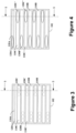
- FIGURE 4 shows the semiconductor power device formed on die 102 of FIGURE 2A , with elongated bumps 120A', 120B', and 120C' (as an alternative to the ball bumps shown in FIGURE 3 ) formed on metal contact regions 110A, 110B, and 110C, respectively.
- the lead-frame 104 may be coupled to the elongated bumps 120A', 120B', and 120C' in a similar manner as discussed above.
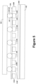
- FIGURE 5 is a cross sectional view of the assembled lead frame and semiconductor power device taken through line "5-5" in either FIGURE 3 or FIGURE 4 .
- the semiconductor power device includes a second metal layer including source metal2 lines 1 10C, drain metal2 lines 110B, and gate metal2 lines 110A formed over a first metal layer including source metal1 lines 130C (as well as drain metal1 lines and gate metal1 lines, which are not shown in this view), wherein the source metal2 lines 110C of the second metal layer are connected to underlying source metal 1 lines 130C of the first metal layer by conductive vias 140.
- a passivation layer 150 formed over the second metal layer includes passivation openings 152 through which bumps 120 or 120' extend into contact with the respective underlying metal contact region of the second metal layer, in this view source metal2 lines 110C.
- the lead frame 104 is arranged in contact with the bumps 120 or 120', thereby conductively connecting the lead-frame to the semiconductor power device.
- FIGURE 6 shows a schematic plan view of the example dual-metal-layer semiconductor power device of FIGURE 5 , showing the arrangement of the second metal layer over the first metal layer, and showing both source metal1 lines 130C and drain metal1 lines 130B of the first metal layer.
- the vias 140 connecting the respective metal 1 and metal2 layers are not shown in Fig. 6 .
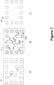
- FIGURES 7A-7C show an example of using bumps to interconnect separate metal contact regions/lines of the semiconductor device, while providing connection to the lead frame.
- FIGURE 7A shows a schematic plan view of a semiconductor die 10 having an array of passivation openings 12 formed in a passivation layer, each opening to an underlying metal contact region, e.g., as discussed above regarding FIGURE 1A .
- the metal layers underlying the openings 12 may not be connected.
- conventional devices would require an additional metal layer. According to this example which is not considered to form part of the invention, such additional layers can be avoided.
- FIGURE 7B shows the semiconductor die 10 of FIGURE 1A with ball bumps 200 formed in some passivation openings 12, and interconnecting bumps 200a', 200c', 200e' formed in other passivation openings 12a-f and extending over the passivation layer to connect two or more underlying metal contact regions.
- interconnecting bump 200a' connects the two metal layers through passivation layer openings 12a and 12b.
- Interconnecting bump 200c' connects the two metal layers through passivation layer openings 12c and 12d
- interconnecting bump 200e' connects the two metal layers through passivation layer openings 12e and 12f.
- Other configurations are possible and an interconnecting bump 200' may also connect more than two underlying metal layers.
- FIGURE 7C shows a lead frame 20 having a corresponding pattern to be connected to the bumps 200 and 200', thereby forming contact between the underlying metal contact regions of the semiconductor die 10 and the lead frame 20.
- Each interconnecting bump 200' may connect any suitable number of underlying metal contact regions, e.g., two, three, four, or more contact regions.
- a particular configuration may include both interconnecting bumps 200' and non-interconnecting bumps 200 (e.g., the ball bumps shown in FIGURE 7B ), or may include only interconnecting bumps 200'.
- Interconnecting bumps 200' may thus provide routing in the bump layer, which may replace one layer of metal interconnect.
- the semiconductor device may need only a single metal interconnect layer, as opposed to the two metal layers included in the design of FIGURES 5 and 6 , which reduction of a metal layer may reduce fabrication costs.
- the use of such interconnecting bumps 200' may provide a "top metal layer" with lower resistance, as compared with the design of FIGURES 5 and 6 .
- FIGURE 8 shows a schematic plan view of an example arrangement of interconnecting bumps 200' on a single-metal-interconnect-layer semiconductor device 210, e.g., a power-FET device, according to one example embodiment.
- device 210 includes a single metal interconnect layer including a gate metal line 230A, drain metal lines 230B, and source metal lines 230C.
- a bump 200A is formed over, and in connection with, gate metal line 230A via a corresponding passivation opening 260.
- the passivation opening 260 may be adapted in size depending on the size of the respective metal line 230A, 230B, 230C.
- a plurality of drain interconnection bumps 200B' are formed to interconnect separate drain metal lines 230B via respective passivation openings, and a plurality of source interconnection bumps 200C' are formed to interconnect separate source metal lines 230C via respective passivation openings.
- FIGURE 9 is a cross sectional view of semiconductor power device 210 of FIGURE 8 , taken through line "9-9" shown in FIGURE 8 , and showing a lead frame 104 assembled to the semiconductor power device 210, in a flip-chip mounting configuration.
- the semiconductor power device 210 includes a single metal interconnect layer including source metal1 lines 230C, drain metal1 lines 230B, and gate metal2 line(s) (not shown), formed on a semiconductor die 240.
- a passivation layer 250 formed over the metal interconnect layer includes passivation openings 252 through which source interconnection bumps 200C' extend into contact with multiple separate underlying source metal 1 lines 230C, such that each source interconnection bump 200C' connects multiple source metal1 lines 230C to the lead-frame, thereby providing routing in the bump layer, and allowing for the elimination of a second metal interconnect layer, as discussed above.
- FIG. 10 shows a first example of a chip 530 mounted on a lead-frame 510 as explained above.
- the lead-frame may have a plurality of external pins 570, in the shown example 8 pins.
- the power transistor chip 530 shown uses four pins 570 for the drain connection and three pins 570 for the source connection.
- a single pin is used for the gate connection.
- the lead-frame may comprise a plurality of support connections, three of which are referenced by reference symbol 540.
- the pins 570 for the external connection may be single pins or form a group of connected pins as shown in FIG. 10 . Thus, any support connection between these pins within a group may remain. Also according to other embodiments, wider pins may be used for the source drain connection to support a higher current.
- control circuits in particular microcontroller applications, require the control of power transistors, for example, switch mode power supply controllers, buck converters or motor control applications. Such applications therefore use generally separate discrete power transistors.
- a pulse width modulator or even a microcontroller can be packaged together with a power transistor as described above.
- FIG. 11 shows an example of a lead-frame 610 that can support a first chip 620, for example a microcontroller chip, coupled to the lead-frame 610 in conventional bonding technique and a second chip 530 comprising one a power transistor as described above and mounted to the lead-frame using the above mentioned flip chip bump bonding technique.
- Reference symbol 570 again indicates an external pin of the lead-frame 510.
- Lead-frame 610 is furthermore shown in FIG. 11 with a plurality of support connections, four of them indicated by reference symbol 540. As mentioned above, these support structures are cut out before enclosing the device in a housing to eliminate any unwanted shorts in the frame and proper connection to the designated pin 570.
- the first chip 620 can be interconnected to at least one of the source, drain and gate fingers at appropriate connection points on the lead-frame 610. While the first chip 620 uses single pins 570 for each connection to a bond pad 650, the section of the lead-frame for the second chip may again connect multiple pins 570 to each source and drain connection to provide a low resistance and support for high currents. However, other external pins, for example, wider pins may be used for the source and/or drain contacts of the second chip 530 according to various embodiments. As mentioned above, the first chip 520 can be a pulse width modulation device, a controller or a microcontroller operable to directly interface with a power transistor. To this end, these devices have integrated drivers that are capable of directly driving the gate of the power transistor.
- FIG. 12 shows yet another embodiment comprising a lead-frame 710 with a microcontroller chip 620 connected by standard wire-bonding and two power transistor chips 720 and 730 mounted in flip chip technology as explained above.
- the section on the right comprises the two power transistors.
- additional external pins 710 are provided in comparison with FIG. 11 for coupling with the interconnected source-drain section 310 via bonding wires 750.
- Any source, drain and/or gate of the two transistor chips 720, 730 may be connected to a bond pad 650 via a bond wire 740 of the microcontroller chip 620 as exemplarily shown in FIG. 12 .
- FIG. 12 shows a plurality of support structures 540 that will be removed before encapsulation.
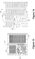
- Fig. 13 shows yet another embodiment comprising a lead-frame 810 with a microcontroller chip 820 or any other control unit as suitable and two power transistor chips 830 and 840.
- all chips are mounted in flip chip technology as explained above.
- the controller chip 820 is also designed in flip chip technology.
- the lead frame 810 is used to provide for the interconnections between the microcontroller chip 820 and the two power transistors 830 and 840.
- the controller chip 820 uses a redistribution layer and is then bumped to the lead frame 810. It's then placed on the lead frame and the lead frame is etched to provide the routing.
- the power transistor 840 is twice the size of the power transistor 830.
- the lower FET with its source connected to ground is two time times the upper FET which is coupled with the supply voltage Vin.
- such an application may use a supply voltage of 12V in and 0.8 to 2.5 output voltage Vout in a switch mode power supply.
- Fig. 13 merely shows one possible arrangement.
- Fig. 14 shows only the lead frame 810 of Fig. 13 alone, wherein the parts 910 that will be finally exposed in the packaged integrated circuit are shaded darker than the other parts 920 of the lead frame. Thus, only the darker shaded areas 910 will get soldered down on a printed circuit board.
- the lighter green areas 920 are still lead-frame, but they are only exposed inside the package where the respective dies will be flipped onto, or they are used for routing signals , in particular for the microcontroller chip 820.
- connection fingers are used to provide a large external connection area for the power transistors 830 and 840 suitable to carry large currents, wherein small square connection pads are provided for the microcontroller chip 820.
- Numeral 930 shows the gate connection to the respective transistors 830 and 840 and the respective connections to the controller chip 820.
- the gate connection is also externally accessible through respective small pads 940 which are here associated with the controller chip 820.
- Fig. 15 shows another example of how a power transistor chip 830 can be mounted and connected to in flip chip technology within a package.
- the vertical lines 1010 are the fab metal1 lines
- the ovals 1020, 1040 are the bumps
- the smaller squares 1030 are the passivation openings.
- Fig. 15 shows how the bump interconnect the individual metal1 lines in one possible arrangement.
- each bump 1020 associated with the drain or source fingers connects multiple fingers, for example 5 fingers wherein the bumps 1040 only use a single opening 1030 to connect to the respective gate fingers.
- This chip 830 is then flipped over onto the stripes of an associated lead-frame 810 as shown in Fig. 13 .
- Fig. 16 shows a bottom view of a microcontroller chip 820 with only the connection pads 1050 showing.
- Fig. 17 shows an enlarged section of Fig. 13 with the microcontroller placed on the lead frame. Similar as shown in Fig. 17 , the chips 820-840 are indicated to be arranged under the lead frame 810.
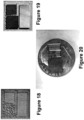
- Fig. 18 shows an actual picture of a lead frame by itself before mounting. The with areas are the areas exposed for external connection.
- Fig. 19 shows the lead frame with 3 semiconductor chips flipped and mounted thereon.
- Fig. 20 shows a top view two final integrated circuit package, wherein one chip has been turned upside down, in comparison to a coin.
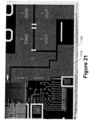
- Fig. 21 shows an exemplary design of a printed circuit board as shown in a respective CAD program. As can be seen large connection areas 1110 and 1120 are provided to connect to the lead frame areas provided for the source and drain for the lower FET 840.
- controller chip and power transistors as shown in the embodiments of Figs. 13-20 can also be applied to a controller and a single power transistor as shown in Fig. 11 .
- the embodiments shown in the various figures are not restricted to field effect transistors but may also be used for any type of bipolar transistor structure.
Landscapes
- Semiconductor Integrated Circuits (AREA)
- Insulated Gate Type Field-Effect Transistor (AREA)
- Engineering & Computer Science (AREA)
- Microelectronics & Electronic Packaging (AREA)
- Internal Circuitry In Semiconductor Integrated Circuit Devices (AREA)
- Junction Field-Effect Transistors (AREA)
Description
- The present disclosure relates to semiconductor devices, e.g., power-FETs or other semiconductor power devices, and more particularly to fabrication of a semiconductor power device to a lead-frame using bump bonds that act as interconnects between separate metal lines.
- Semiconductor power devices typically operate at high current densities, and as such, require current carrying conductors having low enough contact resistances to adequately handle the current to and from the device. There are limitations, however, for metal deposition thickness during fabrication of the semiconductor power device. This metal deposition thickness limitation necessitates having to deposit metal conductors on both the front and back sides of the semiconductor power device, e.g., power field effect transistor (power-FET). But having to use back side contact of the power element(s) of the device, e.g., drain requires extensive processing to eliminate the series resistance of the semiconductor substrate, thereby adding significant cost to the final semiconductor power product.
- US Patent
US 7,560,808 discloses a chip scale power LDMOS device. - Therefore, it is desired to reduce processing steps in manufacturing a semiconductor power device, and thereby reduce manufacturing costs thereof.
- The invention is defined by the independent claim.
- Further enhancements are characterized in the dependent claims.
-
Fig. 1A , B, C show a conventional semiconductor die having an array of passivation openings, solder bumps and lead frame; -
Fig. 2A , B show a conventional power transistor die and associated lead frame; -
Fig. 3 and 4 show conventional arrangement of bumps on power transistor dies; -
Fig. 5 shows a sectional view along lines 5-5 ofFigs. 3 and 4 of a conventional power transistor die mounted on a lead frame in flip chip technology; -
Fig. 6 shows a top view of metal layers of a conventional power transistor die; -
Fig. 7 A, B, C show a semiconductor die having an array of passivation openings, associated solder bumps, and leadframe, according to an example not forming part of the invention; -
Fig. 8 shows a top view of a power transistor chip according to various embodiments; -
Fig. 9 shows a sectional view along lines 9-9 ofFig. 8 ; -
Fig. 10-12 show examples of lead frames with power transistors according to some embodiments; -
Fig. 13 and 14 show a lead frame and power transistor chips arrangement according to some embodiments; -
Fig. 15 shows a power transistor according to yet another embodiment; -
Fig. 16 and 17 show a microcontroller chip and placement on a lead frame in flip-chip technology; -
Fig. 18 shows a photo of a lead frame according to an embodiment; -
Fig. 19 shows a photo of a lead frame with mounted chips according to an embodiment; -
Fig. 20 shows a photo of multi-die integrated circuits in top and bottom view according to an embodiment; -
Fig. 21 shows an exemplary layout of a printed circuit board designed to receive an integrated circuit as shown inFig. 20 . - As disclosed in
US application 13/288,108 filed on November 3, 2011 US 2012/0126406 (hereinafter "the '108 Application"), a semiconductor power chip may have a semiconductor die having a power device fabricated on a substrate thereof, which power device is conductively connected to a corresponding lead-frame by an array of bump bonds, e.g., ball bumps or loaf bumps. For example, a semiconductor power chip may have a semiconductor die having a power device fabricated on a substrate thereof, wherein the power device has a plurality of gate metal contact regions, source metal contact regions, and drain metal contact regions arranged on top of the semiconductor die. A plurality of ball bumps or a loaf bump may be disposed on each metal contact region, and a lead-frame having an area comprising gate, source, and drain lead-fingers that match up with the plurality of ball bumps or the loaf bump for connecting to each of the metal contact regions. - As discussed in the '108 Application, using a bump or loaf array to distribute the current between elements of the semiconductor power device and a much thicker lead-frame eliminates the need for a separate backside contact and subsequent processing step(s). The bump or loaf array may comprise a single loaf bump or a plurality of ball bumps arranged in a "bump loaf" configuration on each of the semiconductor elements. The semiconductor power device may then be attached to a lead-frame using flip-chip ball bond techniques. This results in lower processing and manufacturing costs, and a smaller form-factor for the semiconductor power device. Low resistance substrates are not needed and an epitaxial silicon growth step is eliminated. Such a mounted power device can be combined and connected to a second chip within a housing, wherein the second chip may comprise a microcontroller or pulse width modulation controller.
- The present disclosure provides further inventive improvements to the concepts disclosed in the '108 Application. For example, the present disclosure provides a method for forming bump bonds ("bumps") that not only allow connection of the semiconductor device to the lead-frame, but also act as interconnections between separate fab metal lines. In addition, the bumps can be used to interconnect a plurality of lead-frame traces to a single fab metal line. These concepts are discussed below, after a discussion of the relevant existing technology.
-
FIGURE 1A shows a general schematic plan view of asemiconductor die 10 having an array ofpassivation openings 12 formed in a passivation layer, eachpassivation openings 12 opening to an underlying metal contact region (e.g., gate, source, or drain metal contact region).FIGURE 1B shows the semiconductor die 10 ofFIGURE 1A withconductive bumps 14 formed in each passivation opening 12.FIGURE 1C shows alead frame 20 having a corresponding pattern to be connected to thebumps 12 shown inFIGURE 1B , thereby forming contact between the underlying metal contact regions of thesemiconductor die 10 and thelead frame 20. -
FIGURES 2A and 2B show a schematic plan view of a semiconductor power device and a plan view of a corresponding lead-frame, respectively, e.g., according to the '108 Application. As shown inFIGURE 2A , a power semiconductor die 102 may comprise a gate (G)metal contact region 110A, drain (D)metal contact regions 110B, and source (S)metal contact regions 110C. The elongated metal contact regions 110 may be referred to as "fingers." The bump metal fingers 110 can be formed by a patterned metal layers deposited on the top of the interconnect metal layers, for example, on the top of the second metal layer. For example, the source and drain regions may be connected to metal runners on a first metal layer, then a second layer of metal may form wider metal runners that will be where the bump metal of the top contacts will be deposited. - As shown in
FIGURE 2B , a corresponding lead-frame 104 having a conductive frame and lead-fingers is adapted to be coupled to the semiconductor power device via a plurality of conductive bumps arranged on the variousmetal contact regions frame 104 shown inFIG. 1 is depicted in a "final state," in other words, any support joints between the fingers have been removed. -
FIGURE 3 shows the semiconductor power device formed on die 102 ofFIGURE 2A , withball bumps metal contact regions frame 104 may be arranged over thesemiconductor die 102 in a "flip-chip" configuration, with the fingers of the lead-frame 104 contacting therespective ball bumps drain ball bumps 110B, and source lead-fingers connect to thesource ball bumps 110C, e.g., as discussed in the '108 Application. -
FIGURE 4 shows the semiconductor power device formed on die 102 ofFIGURE 2A , withelongated bumps 120A', 120B', and 120C' (as an alternative to the ball bumps shown inFIGURE 3 ) formed onmetal contact regions frame 104 may be coupled to theelongated bumps 120A', 120B', and 120C' in a similar manner as discussed above. -
FIGURE 5 is a cross sectional view of the assembled lead frame and semiconductor power device taken through line "5-5" in eitherFIGURE 3 or FIGURE 4 . As shown, the semiconductor power device includes a second metal layer includingsource metal2 lines 1 10C,drain metal2 lines 110B, andgate metal2 lines 110A formed over a first metal layer includingsource metal1 lines 130C (as well as drain metal1 lines and gate metal1 lines, which are not shown in this view), wherein thesource metal2 lines 110C of the second metal layer are connected to underlyingsource metal 1lines 130C of the first metal layer byconductive vias 140. - A
passivation layer 150 formed over the second metal layer includespassivation openings 152 through whichbumps 120 or 120' extend into contact with the respective underlying metal contact region of the second metal layer, in this viewsource metal2 lines 110C. Finally, thelead frame 104 is arranged in contact with thebumps 120 or 120', thereby conductively connecting the lead-frame to the semiconductor power device. -
FIGURE 6 shows a schematic plan view of the example dual-metal-layer semiconductor power device ofFIGURE 5 , showing the arrangement of the second metal layer over the first metal layer, and showing bothsource metal1 lines 130C and drainmetal1 lines 130B of the first metal layer. Thevias 140 connecting therespective metal 1 and metal2 layers are not shown inFig. 6 . -
FIGURES 7A-7C show an example of using bumps to interconnect separate metal contact regions/lines of the semiconductor device, while providing connection to the lead frame.FIGURE 7A shows a schematic plan view of asemiconductor die 10 having an array ofpassivation openings 12 formed in a passivation layer, each opening to an underlying metal contact region, e.g., as discussed above regardingFIGURE 1A . Within the semiconductor, the metal layers underlying theopenings 12 may not be connected. Thus, conventional devices would require an additional metal layer. According to this example which is not considered to form part of the invention, such additional layers can be avoided. -
FIGURE 7B shows the semiconductor die 10 ofFIGURE 1A with ball bumps 200 formed in somepassivation openings 12, and interconnectingbumps 200a', 200c', 200e' formed inother passivation openings 12a-f and extending over the passivation layer to connect two or more underlying metal contact regions. Thus, interconnectingbump 200a' connects the two metal layers throughpassivation layer openings bump 200c' connects the two metal layers throughpassivation layer openings bump 200e' connects the two metal layers throughpassivation layer openings -
FIGURE 7C shows alead frame 20 having a corresponding pattern to be connected to thebumps 200 and 200', thereby forming contact between the underlying metal contact regions of the semiconductor die 10 and thelead frame 20. Each interconnecting bump 200' may connect any suitable number of underlying metal contact regions, e.g., two, three, four, or more contact regions. Also, a particular configuration may include both interconnecting bumps 200' and non-interconnecting bumps 200 (e.g., the ball bumps shown inFIGURE 7B ), or may include only interconnecting bumps 200'. - Interconnecting bumps 200' may thus provide routing in the bump layer, which may replace one layer of metal interconnect. Thus, the semiconductor device may need only a single metal interconnect layer, as opposed to the two metal layers included in the design of
FIGURES 5 and6 , which reduction of a metal layer may reduce fabrication costs. In addition, the use of such interconnecting bumps 200' may provide a "top metal layer" with lower resistance, as compared with the design ofFIGURES 5 and6 . -
FIGURE 8 shows a schematic plan view of an example arrangement of interconnecting bumps 200' on a single-metal-interconnect-layer semiconductor device 210, e.g., a power-FET device, according to one example embodiment. As shown,device 210 includes a single metal interconnect layer including agate metal line 230A, drainmetal lines 230B, andsource metal lines 230C. Abump 200A is formed over, and in connection with,gate metal line 230A via a correspondingpassivation opening 260. Thepassivation opening 260 may be adapted in size depending on the size of therespective metal line drain metal lines 230B via respective passivation openings, and a plurality of source interconnection bumps 200C' are formed to interconnect separatesource metal lines 230C via respective passivation openings. -
FIGURE 9 is a cross sectional view ofsemiconductor power device 210 ofFIGURE 8 , taken through line "9-9" shown inFIGURE 8 , and showing alead frame 104 assembled to thesemiconductor power device 210, in a flip-chip mounting configuration. As shown, thesemiconductor power device 210 includes a single metal interconnect layer including source metal1 lines 230C, drainmetal1 lines 230B, and gate metal2 line(s) (not shown), formed on asemiconductor die 240. Apassivation layer 250 formed over the metal interconnect layer includespassivation openings 252 through which source interconnection bumps 200C' extend into contact with multiple separateunderlying source metal 1lines 230C, such that eachsource interconnection bump 200C' connects multiple source metal1 lines 230C to the lead-frame, thereby providing routing in the bump layer, and allowing for the elimination of a second metal interconnect layer, as discussed above. -
FIG. 10 shows a first example of achip 530 mounted on a lead-frame 510 as explained above. The lead-frame may have a plurality ofexternal pins 570, in the shown example 8 pins. Thepower transistor chip 530 shown uses fourpins 570 for the drain connection and threepins 570 for the source connection. A single pin is used for the gate connection. For mounting purposes and before encapsulation, the lead-frame may comprise a plurality of support connections, three of which are referenced byreference symbol 540. Thepins 570 for the external connection may be single pins or form a group of connected pins as shown inFIG. 10 . Thus, any support connection between these pins within a group may remain. Also according to other embodiments, wider pins may be used for the source drain connection to support a higher current. - Certain applications of control circuits, in particular microcontroller applications, require the control of power transistors, for example, switch mode power supply controllers, buck converters or motor control applications. Such applications therefore use generally separate discrete power transistors. According to various embodiments, a pulse width modulator or even a microcontroller can be packaged together with a power transistor as described above.
-
FIG. 11 shows an example of a lead-frame 610 that can support afirst chip 620, for example a microcontroller chip, coupled to the lead-frame 610 in conventional bonding technique and asecond chip 530 comprising one a power transistor as described above and mounted to the lead-frame using the above mentioned flip chip bump bonding technique.Reference symbol 570 again indicates an external pin of the lead-frame 510. Lead-frame 610 is furthermore shown inFIG. 11 with a plurality of support connections, four of them indicated byreference symbol 540. As mentioned above, these support structures are cut out before enclosing the device in a housing to eliminate any unwanted shorts in the frame and proper connection to the designatedpin 570. As shown thefirst chip 620 can be interconnected to at least one of the source, drain and gate fingers at appropriate connection points on the lead-frame 610. While thefirst chip 620 usessingle pins 570 for each connection to abond pad 650, the section of the lead-frame for the second chip may again connectmultiple pins 570 to each source and drain connection to provide a low resistance and support for high currents. However, other external pins, for example, wider pins may be used for the source and/or drain contacts of thesecond chip 530 according to various embodiments. As mentioned above, the first chip 520 can be a pulse width modulation device, a controller or a microcontroller operable to directly interface with a power transistor. To this end, these devices have integrated drivers that are capable of directly driving the gate of the power transistor. -
FIG. 12 shows yet another embodiment comprising a lead-frame 710 with amicrocontroller chip 620 connected by standard wire-bonding and two power transistor chips 720 and 730 mounted in flip chip technology as explained above. The section on the right comprises the two power transistors. Here, additionalexternal pins 710 are provided in comparison withFIG. 11 for coupling with the interconnected source-drain section 310 viabonding wires 750. Any source, drain and/or gate of the twotransistor chips bond pad 650 via abond wire 740 of themicrocontroller chip 620 as exemplarily shown inFIG. 12 . Again,FIG. 12 shows a plurality ofsupport structures 540 that will be removed before encapsulation. -
Fig. 13 shows yet another embodiment comprising a lead-frame 810 with amicrocontroller chip 820 or any other control unit as suitable and two power transistor chips 830 and 840. In this embodiment, all chips are mounted in flip chip technology as explained above. As can be seen in this embodiment, no bond wires are used at all. Thus, thecontroller chip 820 is also designed in flip chip technology. Thelead frame 810 is used to provide for the interconnections between themicrocontroller chip 820 and the twopower transistors controller chip 820 uses a redistribution layer and is then bumped to thelead frame 810. It's then placed on the lead frame and the lead frame is etched to provide the routing. - As can be seen in
Fig. 13 , in this embodiment, thepower transistor 840 is twice the size of thepower transistor 830. For some applications the lower FET with its source connected to ground is two time times the upper FET which is coupled with the supply voltage Vin. For example, such an application may use a supply voltage of 12V in and 0.8 to 2.5 output voltage Vout in a switch mode power supply. However, other dimensions for the FETs may be chosen andFig. 13 merely shows one possible arrangement. -
Fig. 14 shows only thelead frame 810 ofFig. 13 alone, wherein theparts 910 that will be finally exposed in the packaged integrated circuit are shaded darker than theother parts 920 of the lead frame. Thus, only the darkershaded areas 910 will get soldered down on a printed circuit board. The lightergreen areas 920 are still lead-frame, but they are only exposed inside the package where the respective dies will be flipped onto, or they are used for routing signals , in particular for themicrocontroller chip 820. - Thus, elongated strips and parts of the respective connection fingers are used to provide a large external connection area for the
power transistors microcontroller chip 820.Numeral 930 shows the gate connection to therespective transistors controller chip 820. The gate connection is also externally accessible through respectivesmall pads 940 which are here associated with thecontroller chip 820. -
Fig. 15 shows another example of how apower transistor chip 830 can be mounted and connected to in flip chip technology within a package. Thevertical lines 1010 are the fab metal1 lines, theovals smaller squares 1030 are the passivation openings. Thus,Fig. 15 shows how the bump interconnect the individual metal1 lines in one possible arrangement. As can be seen in this embodiment, eachbump 1020 associated with the drain or source fingers connects multiple fingers, for example 5 fingers wherein thebumps 1040 only use asingle opening 1030 to connect to the respective gate fingers. Thischip 830 is then flipped over onto the stripes of an associated lead-frame 810 as shown inFig. 13 . -
Fig. 16 shows a bottom view of amicrocontroller chip 820 with only theconnection pads 1050 showing.Fig. 17 shows an enlarged section ofFig. 13 with the microcontroller placed on the lead frame. Similar as shown inFig. 17 , the chips 820-840 are indicated to be arranged under thelead frame 810. -
Fig. 18 shows an actual picture of a lead frame by itself before mounting. The with areas are the areas exposed for external connection.Fig. 19 shows the lead frame with 3 semiconductor chips flipped and mounted thereon.Fig. 20 shows a top view two final integrated circuit package, wherein one chip has been turned upside down, in comparison to a coin.Fig. 21 shows an exemplary design of a printed circuit board as shown in a respective CAD program. As can be seenlarge connection areas lower FET 840. - The principle arrangement of controller chip and power transistors as shown in the embodiments of
Figs. 13-20 can also be applied to a controller and a single power transistor as shown inFig. 11 . The embodiments shown in the various figures are not restricted to field effect transistors but may also be used for any type of bipolar transistor structure.
Claims (9)
- A semiconductor power device (210) comprising:a semiconductor die (240) with an array of conductive contact elements (230A, B, C; 1010) formed thereon, wherein the array of conductive contact elements (230A, B, C; 1010) comprises at least one gate contact element (230A; 1010), a plurality of elongated source contact strips (230C; 1010), and a plurality of elongated drain contact strips (230B; 1010), wherein the plurality of elongated source and drain contact strips (230B, 230C; 1010) are arranged in parallel and alternatingly next to each other;a passivation layer (250) formed over the array of conductive contact elements (230A, B, C; 1010), the passivation layer (250) comprising passivation openings (252; 260; 1030) over the array of conductive contact elements (230A, B, C; 1010); andan array of conductive bumps (200A; 200B'; 200C'; 1020, 1040) including at least one gate bump (200A; 1040), a plurality of source interconnection bumps (200C'; 1020) and a plurality of drain interconnection bumps (200B'; 1020) formed over the passivation layer (250), wherein the at least one gate bump (200A; 1040) connects via a single passivation opening (260; 1030) with an underlying gate contact element (230A; 1010), wherein each source interconnection bump (200C'; 1020) extends into at least two of the passivation openings (252; 260; 1030) and into contact with at least two underlying source contact strips (230C; 1010) to thereby provide a conductive coupling between the at least two underlying source contact strips (230C; 1010) between which a drain contact strip (230B; 1010) is arranged;characterized bya lead frame (104; 510; 610; 710; 810) having an area comprising source, drain and gate lead-fingers coupled to the array of conductive bumps (200A, 200B', 200C'; 1020, 1040), wherein the source, drain and gate lead-fingers are conductively coupled to each of the source contact strips (230C; 1010), the drain contact strips (230B; 1010) and the at least one gate contact element (230A; 1010), respectively, through the corresponding source, drain and gate bumps (200A; 200B'; 200C'; 1020, 1040) of the array of conductive bumps and wherein the source and drain lead-fingers are perpendicular to the source and drain contact strips (230B, C; 1010), respectively;wherein only a single metal interconnect layer is provided, which includes the array of conductive contact elements (230A, B, C; 1010);wherein each drain interconnection bump (200B'; 1020) extends into at least two of the passivation openings (260; 1030) and into contact with at least two underlying drain contact strips (230B; 1010) to thereby provide a conductive coupling between the at least two underlying drain contact strips (230C; 1010) between which a source contact strip (230C; 1010) is arranged,wherein the drain and source interconnection bumps (200B', 200C'; 1020) are alternatingly arranged along adjacent elongated source and drain contact strips (230B, 230C; 1010) arranged in parallel.
- The semiconductor power device of Claim 1, wherein each source interconnection bump (1020) connects five source contact strips (1010) arranged in parallel and each drain interconnection bump (1020) connects five drain contact strips (1010) arranged in parallel.
- The semiconductor power device (210) according to one of the preceding claims, wherein the plurality of source interconnection bumps (200C'; 1020) comprises at least one source interconnection bump (200C'; 1020) that provides a conductive coupling between at least two source regions that are otherwise electrically isolated within the semiconductor die (240) and wherein the plurality of drain interconnection bumps (200B'; 1020) comprises at least one drain interconnection bump (200B'; 1020) that provides a conductive coupling between at least two drain regions that are otherwise electrically isolated within the semiconductor die (240).
- The semiconductor power device (210) according to one of the preceding claims, wherein the array of conductive bumps (200A, 200B', 200C'; 1020, 1040) includes a plurality of gate bumps (200A, 1040), each extending into contact with only a single underlying gate contact element (230A, 1010).
- The semiconductor power device according to one of claims 1-4, further comprising
a housing surrounding said semiconductor power die (240) and said lead-frame (104; 510; 610; 710; 810). - A multi-chip semiconductor device comprising a semiconductor power device according to one of claims 1-4, further comprising:another chip (620; 820);wherein the lead-frame (610; 710) also has a second area configured for wire bonding said another chip (620) or wherein said another chip (820) is mounted in flip-chip fashion on the lead frame (810), anda housing surrounding said semiconductor power device, said another chip (620; 820), and said lead-frame (610; 710; 810).
- The semiconductor device according to claim 6, wherein the another chip (620; 820) is a microcontroller chip operable to control said semiconductor power device or a pulse width modulation chip (620) operable to control said semiconductor power device.
- A multi-chip semiconductor device comprising at least a first and second semiconductor power device, each semiconductor power device being formed according to one of the preceding claims 1-4 using the same lead-frame (710; 810), further comprising:a third chip (620; 820);wherein the lead-frame (710; 810) has a first and second area each first and second area comprising gate, source and drain lead-fingers adapted to match up with the array of conductive bumps (200A, 200B', 200C'; 1020, 1040) for connecting to each of the at least one gate contact element (230A; 1010), the plurality of source contact strips (230C; 1010) and the plurality of drain contact strips (230B; 1010) of said first and second semiconductor devices, respectively, and wherein either the lead frame (710) also has a third area configured for wire bonding said third chip (620) or said third chip (820) is mounted in flip-chip fashion on the lead frame (810), anda housing surrounding said first and second semiconductor power devices, said third chip (620; 820) and said lead-frame (710; 810).
- The semiconductor device according to claim 8, wherein the third chip (620; 820) is a microcontroller chip operable to control said first and second semiconductor power devices.
Applications Claiming Priority (3)
| Application Number | Priority Date | Filing Date | Title |
|---|---|---|---|
| US201462002164P | 2014-05-22 | 2014-05-22 | |
| US14/673,347 US9812380B2 (en) | 2014-05-22 | 2015-03-30 | Bumps bonds formed as metal line interconnects in a semiconductor device |
| PCT/US2015/031377 WO2015179294A2 (en) | 2014-05-22 | 2015-05-18 | Bumps bonds formed as metal line interconnects in a semiconductor device |
Publications (2)
| Publication Number | Publication Date |
|---|---|
| EP3146561A2 EP3146561A2 (en) | 2017-03-29 |
| EP3146561B1 true EP3146561B1 (en) | 2024-03-20 |
Family
ID=53274844
Family Applications (1)
| Application Number | Title | Priority Date | Filing Date |
|---|---|---|---|
| EP15725962.3A Active EP3146561B1 (en) | 2014-05-22 | 2015-05-18 | Semiconductor device with bump bonds formed as metal line interconnects |
Country Status (6)
| Country | Link |
|---|---|
| US (1) | US9812380B2 (en) |
| EP (1) | EP3146561B1 (en) |
| KR (1) | KR20170005000A (en) |
| CN (1) | CN106463461B (en) |
| TW (1) | TWI663696B (en) |
| WO (1) | WO2015179294A2 (en) |
Families Citing this family (5)
| Publication number | Priority date | Publication date | Assignee | Title |
|---|---|---|---|---|
| US10163773B1 (en) | 2017-08-11 | 2018-12-25 | General Electric Company | Electronics package having a self-aligning interconnect assembly and method of making same |
| US10847483B2 (en) * | 2018-08-29 | 2020-11-24 | Texas Instruments Incorporated | Integrated circuits with conductive bumps having a profile with a wave pattern |
| US10833036B2 (en) * | 2018-12-27 | 2020-11-10 | Texas Instruments Incorporated | Interconnect for electronic device |
| KR20220090793A (en) | 2020-12-23 | 2022-06-30 | 삼성전자주식회사 | Semiconductor package |
| CN114823593B (en) * | 2022-03-23 | 2026-03-24 | 华为数字能源技术有限公司 | A bidirectional switch packaging structure, semiconductor device, and power converter |
Family Cites Families (17)
| Publication number | Priority date | Publication date | Assignee | Title |
|---|---|---|---|---|
| US6150722A (en) | 1994-11-02 | 2000-11-21 | Texas Instruments Incorporated | Ldmos transistor with thick copper interconnect |
| US5665996A (en) * | 1994-12-30 | 1997-09-09 | Siliconix Incorporated | Vertical power mosfet having thick metal layer to reduce distributed resistance |
| DE19613409B4 (en) * | 1996-04-03 | 2005-11-17 | Texas Instruments Deutschland Gmbh | Power component arrangement |
| US6927491B1 (en) | 1998-12-04 | 2005-08-09 | Nec Corporation | Back electrode type electronic part and electronic assembly with the same mounted on printed circuit board |
| US6645791B2 (en) * | 2001-04-23 | 2003-11-11 | Fairchild Semiconductor | Semiconductor die package including carrier with mask |
| US6969909B2 (en) | 2002-12-20 | 2005-11-29 | Vlt, Inc. | Flip chip FET device |
| JP4294405B2 (en) * | 2003-07-31 | 2009-07-15 | 株式会社ルネサステクノロジ | Semiconductor device |
| JP4130668B2 (en) | 2004-08-05 | 2008-08-06 | 富士通株式会社 | Substrate processing method |
| JP2006128543A (en) * | 2004-11-01 | 2006-05-18 | Nec Electronics Corp | Manufacturing method of electronic device |
| JP4357434B2 (en) * | 2005-02-25 | 2009-11-04 | 株式会社東芝 | Manufacturing method of semiconductor device |
| US7560808B2 (en) | 2005-10-19 | 2009-07-14 | Texas Instruments Incorporated | Chip scale power LDMOS device |
| US7944048B2 (en) * | 2006-08-09 | 2011-05-17 | Monolithic Power Systems, Inc. | Chip scale package for power devices and method for making the same |
| JP2009170747A (en) * | 2008-01-18 | 2009-07-30 | Toshiba Corp | Semiconductor device and manufacturing method thereof |
| JP2011100932A (en) * | 2009-11-09 | 2011-05-19 | Toshiba Corp | Semiconductor package and dc-dc converter |
| JP5457292B2 (en) * | 2010-07-12 | 2014-04-02 | パナソニック株式会社 | Nitride semiconductor device |
| US9093433B2 (en) | 2010-11-18 | 2015-07-28 | Microchip Technology Incorporated | Using bump bonding to distribute current flow on a semiconductor power device |
| CN102110691A (en) * | 2010-12-03 | 2011-06-29 | 杭州矽力杰半导体技术有限公司 | Power field effect transistor and layout method thereof |
-
2015
- 2015-03-30 US US14/673,347 patent/US9812380B2/en active Active
- 2015-05-18 EP EP15725962.3A patent/EP3146561B1/en active Active
- 2015-05-18 CN CN201580026338.7A patent/CN106463461B/en active Active
- 2015-05-18 WO PCT/US2015/031377 patent/WO2015179294A2/en not_active Ceased
- 2015-05-18 KR KR1020167031660A patent/KR20170005000A/en not_active Withdrawn
- 2015-05-22 TW TW104116554A patent/TWI663696B/en active
Also Published As
| Publication number | Publication date |
|---|---|
| EP3146561A2 (en) | 2017-03-29 |
| WO2015179294A3 (en) | 2016-01-14 |
| KR20170005000A (en) | 2017-01-11 |
| TWI663696B (en) | 2019-06-21 |
| CN106463461A (en) | 2017-02-22 |
| US20160013121A1 (en) | 2016-01-14 |
| CN106463461B (en) | 2019-06-18 |
| TW201603223A (en) | 2016-01-16 |
| WO2015179294A2 (en) | 2015-11-26 |
| US9812380B2 (en) | 2017-11-07 |
Similar Documents
| Publication | Publication Date | Title |
|---|---|---|
| US9698143B2 (en) | Wireless module with active devices | |
| KR101906458B1 (en) | Semiconductor product | |
| CN103975427B (en) | The power management application of interconnection substrate | |
| US8941250B1 (en) | Electronic component package fabrication method and structure | |
| US20160307826A1 (en) | PACKAGING SOLUTIONS FOR DEVICES AND SYSTEMS COMPRISING LATERAL GaN POWER TRANSISTORS | |
| US20110193208A1 (en) | Semiconductor package of a flipped mosfet and its manufacturing method | |
| US9812380B2 (en) | Bumps bonds formed as metal line interconnects in a semiconductor device | |
| US8648449B2 (en) | Electrical connectivity for circuit applications | |
| CN112185931B (en) | semiconductor devices | |
| US10707160B2 (en) | Electrical connectivity of die to a host substrate | |
| US8921986B2 (en) | Insulated bump bonding | |
| TWI619253B (en) | Power metal oxide semiconductor transistor with improved metal contact | |
| US12593738B2 (en) | Flip chip package for semiconductor devices | |
| US9721928B1 (en) | Integrated circuit package having two substrates | |
| US20050230850A1 (en) | Microelectronic assembly having a redistribution conductor over a microelectronic die | |
| HK1073723B (en) | Semiconductor power device having a diamond shaped metal interconnect scheme |
Legal Events
| Date | Code | Title | Description |
|---|---|---|---|
| STAA | Information on the status of an ep patent application or granted ep patent |
Free format text: STATUS: THE INTERNATIONAL PUBLICATION HAS BEEN MADE |
|
| PUAI | Public reference made under article 153(3) epc to a published international application that has entered the european phase |
Free format text: ORIGINAL CODE: 0009012 |
|
| STAA | Information on the status of an ep patent application or granted ep patent |
Free format text: STATUS: REQUEST FOR EXAMINATION WAS MADE |
|
| 17P | Request for examination filed |
Effective date: 20161220 |
|
| AK | Designated contracting states |
Kind code of ref document: A2 Designated state(s): AL AT BE BG CH CY CZ DE DK EE ES FI FR GB GR HR HU IE IS IT LI LT LU LV MC MK MT NL NO PL PT RO RS SE SI SK SM TR |
|
| AX | Request for extension of the european patent |
Extension state: BA ME |
|
| DAV | Request for validation of the european patent (deleted) | ||
| DAX | Request for extension of the european patent (deleted) | ||
| STAA | Information on the status of an ep patent application or granted ep patent |
Free format text: STATUS: EXAMINATION IS IN PROGRESS |
|
| 17Q | First examination report despatched |
Effective date: 20210121 |
|
| GRAP | Despatch of communication of intention to grant a patent |
Free format text: ORIGINAL CODE: EPIDOSNIGR1 |
|
| STAA | Information on the status of an ep patent application or granted ep patent |
Free format text: STATUS: GRANT OF PATENT IS INTENDED |
|
| INTG | Intention to grant announced |
Effective date: 20231016 |
|
| GRAS | Grant fee paid |
Free format text: ORIGINAL CODE: EPIDOSNIGR3 |
|
| GRAA | (expected) grant |
Free format text: ORIGINAL CODE: 0009210 |
|
| STAA | Information on the status of an ep patent application or granted ep patent |
Free format text: STATUS: THE PATENT HAS BEEN GRANTED |
|
| AK | Designated contracting states |
Kind code of ref document: B1 Designated state(s): AL AT BE BG CH CY CZ DE DK EE ES FI FR GB GR HR HU IE IS IT LI LT LU LV MC MK MT NL NO PL PT RO RS SE SI SK SM TR |
|
| REG | Reference to a national code |
Ref country code: GB Ref legal event code: FG4D |
|
| REG | Reference to a national code |
Ref country code: CH Ref legal event code: EP |
|
| REG | Reference to a national code |
Ref country code: IE Ref legal event code: FG4D |
|
| REG | Reference to a national code |
Ref country code: DE Ref legal event code: R096 Ref document number: 602015087977 Country of ref document: DE |
|
| PG25 | Lapsed in a contracting state [announced via postgrant information from national office to epo] |
Ref country code: LT Free format text: LAPSE BECAUSE OF FAILURE TO SUBMIT A TRANSLATION OF THE DESCRIPTION OR TO PAY THE FEE WITHIN THE PRESCRIBED TIME-LIMIT Effective date: 20240320 |
|
| REG | Reference to a national code |
Ref country code: LT Ref legal event code: MG9D |
|
| PG25 | Lapsed in a contracting state [announced via postgrant information from national office to epo] |
Ref country code: GR Free format text: LAPSE BECAUSE OF FAILURE TO SUBMIT A TRANSLATION OF THE DESCRIPTION OR TO PAY THE FEE WITHIN THE PRESCRIBED TIME-LIMIT Effective date: 20240621 |
|
| PG25 | Lapsed in a contracting state [announced via postgrant information from national office to epo] |
Ref country code: HR Free format text: LAPSE BECAUSE OF FAILURE TO SUBMIT A TRANSLATION OF THE DESCRIPTION OR TO PAY THE FEE WITHIN THE PRESCRIBED TIME-LIMIT Effective date: 20240320 Ref country code: RS Free format text: LAPSE BECAUSE OF FAILURE TO SUBMIT A TRANSLATION OF THE DESCRIPTION OR TO PAY THE FEE WITHIN THE PRESCRIBED TIME-LIMIT Effective date: 20240620 |
|
| REG | Reference to a national code |
Ref country code: NL Ref legal event code: MP Effective date: 20240320 |
|
| PG25 | Lapsed in a contracting state [announced via postgrant information from national office to epo] |
Ref country code: RS Free format text: LAPSE BECAUSE OF FAILURE TO SUBMIT A TRANSLATION OF THE DESCRIPTION OR TO PAY THE FEE WITHIN THE PRESCRIBED TIME-LIMIT Effective date: 20240620 Ref country code: NO Free format text: LAPSE BECAUSE OF FAILURE TO SUBMIT A TRANSLATION OF THE DESCRIPTION OR TO PAY THE FEE WITHIN THE PRESCRIBED TIME-LIMIT Effective date: 20240620 Ref country code: LT Free format text: LAPSE BECAUSE OF FAILURE TO SUBMIT A TRANSLATION OF THE DESCRIPTION OR TO PAY THE FEE WITHIN THE PRESCRIBED TIME-LIMIT Effective date: 20240320 Ref country code: HR Free format text: LAPSE BECAUSE OF FAILURE TO SUBMIT A TRANSLATION OF THE DESCRIPTION OR TO PAY THE FEE WITHIN THE PRESCRIBED TIME-LIMIT Effective date: 20240320 Ref country code: GR Free format text: LAPSE BECAUSE OF FAILURE TO SUBMIT A TRANSLATION OF THE DESCRIPTION OR TO PAY THE FEE WITHIN THE PRESCRIBED TIME-LIMIT Effective date: 20240621 Ref country code: FI Free format text: LAPSE BECAUSE OF FAILURE TO SUBMIT A TRANSLATION OF THE DESCRIPTION OR TO PAY THE FEE WITHIN THE PRESCRIBED TIME-LIMIT Effective date: 20240320 Ref country code: BG Free format text: LAPSE BECAUSE OF FAILURE TO SUBMIT A TRANSLATION OF THE DESCRIPTION OR TO PAY THE FEE WITHIN THE PRESCRIBED TIME-LIMIT Effective date: 20240320 |
|
| REG | Reference to a national code |
Ref country code: AT Ref legal event code: MK05 Ref document number: 1668612 Country of ref document: AT Kind code of ref document: T Effective date: 20240320 |
|
| PG25 | Lapsed in a contracting state [announced via postgrant information from national office to epo] |
Ref country code: SE Free format text: LAPSE BECAUSE OF FAILURE TO SUBMIT A TRANSLATION OF THE DESCRIPTION OR TO PAY THE FEE WITHIN THE PRESCRIBED TIME-LIMIT Effective date: 20240320 Ref country code: LV Free format text: LAPSE BECAUSE OF FAILURE TO SUBMIT A TRANSLATION OF THE DESCRIPTION OR TO PAY THE FEE WITHIN THE PRESCRIBED TIME-LIMIT Effective date: 20240320 |
|
| PG25 | Lapsed in a contracting state [announced via postgrant information from national office to epo] |
Ref country code: NL Free format text: LAPSE BECAUSE OF FAILURE TO SUBMIT A TRANSLATION OF THE DESCRIPTION OR TO PAY THE FEE WITHIN THE PRESCRIBED TIME-LIMIT Effective date: 20240320 |
|
| PG25 | Lapsed in a contracting state [announced via postgrant information from national office to epo] |
Ref country code: NL Free format text: LAPSE BECAUSE OF FAILURE TO SUBMIT A TRANSLATION OF THE DESCRIPTION OR TO PAY THE FEE WITHIN THE PRESCRIBED TIME-LIMIT Effective date: 20240320 |
|
| PG25 | Lapsed in a contracting state [announced via postgrant information from national office to epo] |
Ref country code: IS Free format text: LAPSE BECAUSE OF FAILURE TO SUBMIT A TRANSLATION OF THE DESCRIPTION OR TO PAY THE FEE WITHIN THE PRESCRIBED TIME-LIMIT Effective date: 20240720 |
|
| PG25 | Lapsed in a contracting state [announced via postgrant information from national office to epo] |
Ref country code: PT Free format text: LAPSE BECAUSE OF FAILURE TO SUBMIT A TRANSLATION OF THE DESCRIPTION OR TO PAY THE FEE WITHIN THE PRESCRIBED TIME-LIMIT Effective date: 20240722 Ref country code: SM Free format text: LAPSE BECAUSE OF FAILURE TO SUBMIT A TRANSLATION OF THE DESCRIPTION OR TO PAY THE FEE WITHIN THE PRESCRIBED TIME-LIMIT Effective date: 20240320 |
|
| PG25 | Lapsed in a contracting state [announced via postgrant information from national office to epo] |
Ref country code: ES Free format text: LAPSE BECAUSE OF FAILURE TO SUBMIT A TRANSLATION OF THE DESCRIPTION OR TO PAY THE FEE WITHIN THE PRESCRIBED TIME-LIMIT Effective date: 20240320 |
|
| PG25 | Lapsed in a contracting state [announced via postgrant information from national office to epo] |
Ref country code: EE Free format text: LAPSE BECAUSE OF FAILURE TO SUBMIT A TRANSLATION OF THE DESCRIPTION OR TO PAY THE FEE WITHIN THE PRESCRIBED TIME-LIMIT Effective date: 20240320 Ref country code: CZ Free format text: LAPSE BECAUSE OF FAILURE TO SUBMIT A TRANSLATION OF THE DESCRIPTION OR TO PAY THE FEE WITHIN THE PRESCRIBED TIME-LIMIT Effective date: 20240320 |
|
| PG25 | Lapsed in a contracting state [announced via postgrant information from national office to epo] |
Ref country code: AT Free format text: LAPSE BECAUSE OF FAILURE TO SUBMIT A TRANSLATION OF THE DESCRIPTION OR TO PAY THE FEE WITHIN THE PRESCRIBED TIME-LIMIT Effective date: 20240320 |
|
| PG25 | Lapsed in a contracting state [announced via postgrant information from national office to epo] |
Ref country code: PL Free format text: LAPSE BECAUSE OF FAILURE TO SUBMIT A TRANSLATION OF THE DESCRIPTION OR TO PAY THE FEE WITHIN THE PRESCRIBED TIME-LIMIT Effective date: 20240320 |
|
| PG25 | Lapsed in a contracting state [announced via postgrant information from national office to epo] |
Ref country code: SK Free format text: LAPSE BECAUSE OF FAILURE TO SUBMIT A TRANSLATION OF THE DESCRIPTION OR TO PAY THE FEE WITHIN THE PRESCRIBED TIME-LIMIT Effective date: 20240320 |
|
| PG25 | Lapsed in a contracting state [announced via postgrant information from national office to epo] |
Ref country code: SM Free format text: LAPSE BECAUSE OF FAILURE TO SUBMIT A TRANSLATION OF THE DESCRIPTION OR TO PAY THE FEE WITHIN THE PRESCRIBED TIME-LIMIT Effective date: 20240320 Ref country code: SK Free format text: LAPSE BECAUSE OF FAILURE TO SUBMIT A TRANSLATION OF THE DESCRIPTION OR TO PAY THE FEE WITHIN THE PRESCRIBED TIME-LIMIT Effective date: 20240320 Ref country code: RO Free format text: LAPSE BECAUSE OF FAILURE TO SUBMIT A TRANSLATION OF THE DESCRIPTION OR TO PAY THE FEE WITHIN THE PRESCRIBED TIME-LIMIT Effective date: 20240320 Ref country code: PT Free format text: LAPSE BECAUSE OF FAILURE TO SUBMIT A TRANSLATION OF THE DESCRIPTION OR TO PAY THE FEE WITHIN THE PRESCRIBED TIME-LIMIT Effective date: 20240722 Ref country code: PL Free format text: LAPSE BECAUSE OF FAILURE TO SUBMIT A TRANSLATION OF THE DESCRIPTION OR TO PAY THE FEE WITHIN THE PRESCRIBED TIME-LIMIT Effective date: 20240320 Ref country code: IS Free format text: LAPSE BECAUSE OF FAILURE TO SUBMIT A TRANSLATION OF THE DESCRIPTION OR TO PAY THE FEE WITHIN THE PRESCRIBED TIME-LIMIT Effective date: 20240720 Ref country code: ES Free format text: LAPSE BECAUSE OF FAILURE TO SUBMIT A TRANSLATION OF THE DESCRIPTION OR TO PAY THE FEE WITHIN THE PRESCRIBED TIME-LIMIT Effective date: 20240320 Ref country code: EE Free format text: LAPSE BECAUSE OF FAILURE TO SUBMIT A TRANSLATION OF THE DESCRIPTION OR TO PAY THE FEE WITHIN THE PRESCRIBED TIME-LIMIT Effective date: 20240320 Ref country code: CZ Free format text: LAPSE BECAUSE OF FAILURE TO SUBMIT A TRANSLATION OF THE DESCRIPTION OR TO PAY THE FEE WITHIN THE PRESCRIBED TIME-LIMIT Effective date: 20240320 Ref country code: AT Free format text: LAPSE BECAUSE OF FAILURE TO SUBMIT A TRANSLATION OF THE DESCRIPTION OR TO PAY THE FEE WITHIN THE PRESCRIBED TIME-LIMIT Effective date: 20240320 |
|
| PG25 | Lapsed in a contracting state [announced via postgrant information from national office to epo] |
Ref country code: IT Free format text: LAPSE BECAUSE OF FAILURE TO SUBMIT A TRANSLATION OF THE DESCRIPTION OR TO PAY THE FEE WITHIN THE PRESCRIBED TIME-LIMIT Effective date: 20240320 |
|
| REG | Reference to a national code |
Ref country code: DE Ref legal event code: R097 Ref document number: 602015087977 Country of ref document: DE |
|
| REG | Reference to a national code |
Ref country code: CH Ref legal event code: PL |
|
| PG25 | Lapsed in a contracting state [announced via postgrant information from national office to epo] |
Ref country code: IT Free format text: LAPSE BECAUSE OF FAILURE TO SUBMIT A TRANSLATION OF THE DESCRIPTION OR TO PAY THE FEE WITHIN THE PRESCRIBED TIME-LIMIT Effective date: 20240320 |
|
| PG25 | Lapsed in a contracting state [announced via postgrant information from national office to epo] |
Ref country code: MC Free format text: LAPSE BECAUSE OF FAILURE TO SUBMIT A TRANSLATION OF THE DESCRIPTION OR TO PAY THE FEE WITHIN THE PRESCRIBED TIME-LIMIT Effective date: 20240320 |
|
| PG25 | Lapsed in a contracting state [announced via postgrant information from national office to epo] |
Ref country code: DK Free format text: LAPSE BECAUSE OF FAILURE TO SUBMIT A TRANSLATION OF THE DESCRIPTION OR TO PAY THE FEE WITHIN THE PRESCRIBED TIME-LIMIT Effective date: 20240320 |
|
| PG25 | Lapsed in a contracting state [announced via postgrant information from national office to epo] |
Ref country code: LU Free format text: LAPSE BECAUSE OF NON-PAYMENT OF DUE FEES Effective date: 20240518 |
|
| PLBE | No opposition filed within time limit |
Free format text: ORIGINAL CODE: 0009261 |
|
| STAA | Information on the status of an ep patent application or granted ep patent |
Free format text: STATUS: NO OPPOSITION FILED WITHIN TIME LIMIT |
|
| PG25 | Lapsed in a contracting state [announced via postgrant information from national office to epo] |
Ref country code: MC Free format text: LAPSE BECAUSE OF FAILURE TO SUBMIT A TRANSLATION OF THE DESCRIPTION OR TO PAY THE FEE WITHIN THE PRESCRIBED TIME-LIMIT Effective date: 20240320 Ref country code: LU Free format text: LAPSE BECAUSE OF NON-PAYMENT OF DUE FEES Effective date: 20240518 Ref country code: DK Free format text: LAPSE BECAUSE OF FAILURE TO SUBMIT A TRANSLATION OF THE DESCRIPTION OR TO PAY THE FEE WITHIN THE PRESCRIBED TIME-LIMIT Effective date: 20240320 Ref country code: CH Free format text: LAPSE BECAUSE OF NON-PAYMENT OF DUE FEES Effective date: 20240531 |
|
| REG | Reference to a national code |
Ref country code: BE Ref legal event code: MM Effective date: 20240531 |
|
| 26N | No opposition filed |
Effective date: 20241223 |
|
| GBPC | Gb: european patent ceased through non-payment of renewal fee |
Effective date: 20240620 |
|
| PG25 | Lapsed in a contracting state [announced via postgrant information from national office to epo] |
Ref country code: IE Free format text: LAPSE BECAUSE OF NON-PAYMENT OF DUE FEES Effective date: 20240518 |
|
| PG25 | Lapsed in a contracting state [announced via postgrant information from national office to epo] |
Ref country code: SI Free format text: LAPSE BECAUSE OF FAILURE TO SUBMIT A TRANSLATION OF THE DESCRIPTION OR TO PAY THE FEE WITHIN THE PRESCRIBED TIME-LIMIT Effective date: 20240320 Ref country code: BE Free format text: LAPSE BECAUSE OF NON-PAYMENT OF DUE FEES Effective date: 20240531 |
|
| PG25 | Lapsed in a contracting state [announced via postgrant information from national office to epo] |
Ref country code: FR Free format text: LAPSE BECAUSE OF NON-PAYMENT OF DUE FEES Effective date: 20240520 |
|
| PG25 | Lapsed in a contracting state [announced via postgrant information from national office to epo] |
Ref country code: GB Free format text: LAPSE BECAUSE OF NON-PAYMENT OF DUE FEES Effective date: 20240620 |
|
| PGFP | Annual fee paid to national office [announced via postgrant information from national office to epo] |
Ref country code: DE Payment date: 20250423 Year of fee payment: 11 |
|
| PG25 | Lapsed in a contracting state [announced via postgrant information from national office to epo] |
Ref country code: CY Free format text: LAPSE BECAUSE OF FAILURE TO SUBMIT A TRANSLATION OF THE DESCRIPTION OR TO PAY THE FEE WITHIN THE PRESCRIBED TIME-LIMIT; INVALID AB INITIO Effective date: 20150518 |
|
| PG25 | Lapsed in a contracting state [announced via postgrant information from national office to epo] |
Ref country code: HU Free format text: LAPSE BECAUSE OF FAILURE TO SUBMIT A TRANSLATION OF THE DESCRIPTION OR TO PAY THE FEE WITHIN THE PRESCRIBED TIME-LIMIT; INVALID AB INITIO Effective date: 20150518 |
|
| REG | Reference to a national code |
Ref country code: DE Ref legal event code: R079 Ref document number: 602015087977 Country of ref document: DE Free format text: PREVIOUS MAIN CLASS: H01L0023485000 Ipc: H10W0070600000 |