EP3144688A2 - Systems and methods for placing an imaging tool in a test and measurement tool - Google Patents
Systems and methods for placing an imaging tool in a test and measurement tool Download PDFInfo
- Publication number
- EP3144688A2 EP3144688A2 EP16189325.0A EP16189325A EP3144688A2 EP 3144688 A2 EP3144688 A2 EP 3144688A2 EP 16189325 A EP16189325 A EP 16189325A EP 3144688 A2 EP3144688 A2 EP 3144688A2
- Authority
- EP
- European Patent Office
- Prior art keywords
- tool
- test
- imaging tool
- measurement
- imaging
- Prior art date
- Legal status (The legal status is an assumption and is not a legal conclusion. Google has not performed a legal analysis and makes no representation as to the accuracy of the status listed.)
- Granted
Links
Images


Classifications
-
- G—PHYSICS
- G01—MEASURING; TESTING
- G01R—MEASURING ELECTRIC VARIABLES; MEASURING MAGNETIC VARIABLES
- G01R31/00—Arrangements for testing electric properties; Arrangements for locating electric faults; Arrangements for electrical testing characterised by what is being tested not provided for elsewhere
-
- H—ELECTRICITY
- H04—ELECTRIC COMMUNICATION TECHNIQUE
- H04N—PICTORIAL COMMUNICATION, e.g. TELEVISION
- H04N23/00—Cameras or camera modules comprising electronic image sensors; Control thereof
- H04N23/57—Mechanical or electrical details of cameras or camera modules specially adapted for being embedded in other devices
-
- G—PHYSICS
- G01—MEASURING; TESTING
- G01D—MEASURING NOT SPECIALLY ADAPTED FOR A SPECIFIC VARIABLE; ARRANGEMENTS FOR MEASURING TWO OR MORE VARIABLES NOT COVERED IN A SINGLE OTHER SUBCLASS; TARIFF METERING APPARATUS; MEASURING OR TESTING NOT OTHERWISE PROVIDED FOR
- G01D21/00—Measuring or testing not otherwise provided for
- G01D21/02—Measuring two or more variables by means not covered by a single other subclass
-
- G—PHYSICS
- G01—MEASURING; TESTING
- G01J—MEASUREMENT OF INTENSITY, VELOCITY, SPECTRAL CONTENT, POLARISATION, PHASE OR PULSE CHARACTERISTICS OF INFRARED, VISIBLE OR ULTRAVIOLET LIGHT; COLORIMETRY; RADIATION PYROMETRY
- G01J5/00—Radiation pyrometry, e.g. infrared or optical thermometry
- G01J5/02—Constructional details
- G01J5/04—Casings
- G01J5/048—Protective parts
-
- G—PHYSICS
- G01—MEASURING; TESTING
- G01J—MEASUREMENT OF INTENSITY, VELOCITY, SPECTRAL CONTENT, POLARISATION, PHASE OR PULSE CHARACTERISTICS OF INFRARED, VISIBLE OR ULTRAVIOLET LIGHT; COLORIMETRY; RADIATION PYROMETRY
- G01J5/00—Radiation pyrometry, e.g. infrared or optical thermometry
- G01J5/02—Constructional details
- G01J5/08—Optical arrangements
- G01J5/0875—Windows; Arrangements for fastening thereof
-
- G—PHYSICS
- G01—MEASURING; TESTING
- G01J—MEASUREMENT OF INTENSITY, VELOCITY, SPECTRAL CONTENT, POLARISATION, PHASE OR PULSE CHARACTERISTICS OF INFRARED, VISIBLE OR ULTRAVIOLET LIGHT; COLORIMETRY; RADIATION PYROMETRY
- G01J5/00—Radiation pyrometry, e.g. infrared or optical thermometry
- G01J5/10—Radiation pyrometry, e.g. infrared or optical thermometry using electric radiation detectors
- G01J5/12—Radiation pyrometry, e.g. infrared or optical thermometry using electric radiation detectors using thermoelectric elements, e.g. thermocouples
-
- G—PHYSICS
- G01—MEASURING; TESTING
- G01J—MEASUREMENT OF INTENSITY, VELOCITY, SPECTRAL CONTENT, POLARISATION, PHASE OR PULSE CHARACTERISTICS OF INFRARED, VISIBLE OR ULTRAVIOLET LIGHT; COLORIMETRY; RADIATION PYROMETRY
- G01J5/00—Radiation pyrometry, e.g. infrared or optical thermometry
- G01J5/10—Radiation pyrometry, e.g. infrared or optical thermometry using electric radiation detectors
- G01J5/28—Radiation pyrometry, e.g. infrared or optical thermometry using electric radiation detectors using photoemissive or photovoltaic cells
-
- G—PHYSICS
- G01—MEASURING; TESTING
- G01R—MEASURING ELECTRIC VARIABLES; MEASURING MAGNETIC VARIABLES
- G01R15/00—Details of measuring arrangements of the types provided for in groups G01R17/00 - G01R29/00, G01R33/00 - G01R33/26 or G01R35/00
- G01R15/14—Adaptations providing voltage or current isolation, e.g. for high-voltage or high-current networks
-
- G—PHYSICS
- G01—MEASURING; TESTING
- G01R—MEASURING ELECTRIC VARIABLES; MEASURING MAGNETIC VARIABLES
- G01R15/00—Details of measuring arrangements of the types provided for in groups G01R17/00 - G01R29/00, G01R33/00 - G01R33/26 or G01R35/00
- G01R15/14—Adaptations providing voltage or current isolation, e.g. for high-voltage or high-current networks
- G01R15/146—Measuring arrangements for current not covered by other subgroups of G01R15/14, e.g. using current dividers, shunts, or measuring a voltage drop
- G01R15/148—Measuring arrangements for current not covered by other subgroups of G01R15/14, e.g. using current dividers, shunts, or measuring a voltage drop involving the measuring of a magnetic field or electric field
-
- H—ELECTRICITY
- H04—ELECTRIC COMMUNICATION TECHNIQUE
- H04N—PICTORIAL COMMUNICATION, e.g. TELEVISION
- H04N23/00—Cameras or camera modules comprising electronic image sensors; Control thereof
- H04N23/20—Cameras or camera modules comprising electronic image sensors; Control thereof for generating image signals from infrared radiation only
- H04N23/23—Cameras or camera modules comprising electronic image sensors; Control thereof for generating image signals from infrared radiation only from thermal infrared radiation
-
- H—ELECTRICITY
- H04—ELECTRIC COMMUNICATION TECHNIQUE
- H04N—PICTORIAL COMMUNICATION, e.g. TELEVISION
- H04N23/00—Cameras or camera modules comprising electronic image sensors; Control thereof
- H04N23/50—Constructional details
- H04N23/51—Housings
-
- G—PHYSICS
- G01—MEASURING; TESTING
- G01J—MEASUREMENT OF INTENSITY, VELOCITY, SPECTRAL CONTENT, POLARISATION, PHASE OR PULSE CHARACTERISTICS OF INFRARED, VISIBLE OR ULTRAVIOLET LIGHT; COLORIMETRY; RADIATION PYROMETRY
- G01J5/00—Radiation pyrometry, e.g. infrared or optical thermometry
- G01J2005/0077—Imaging
-
- G—PHYSICS
- G01—MEASURING; TESTING
- G01J—MEASUREMENT OF INTENSITY, VELOCITY, SPECTRAL CONTENT, POLARISATION, PHASE OR PULSE CHARACTERISTICS OF INFRARED, VISIBLE OR ULTRAVIOLET LIGHT; COLORIMETRY; RADIATION PYROMETRY
- G01J5/00—Radiation pyrometry, e.g. infrared or optical thermometry
- G01J5/10—Radiation pyrometry, e.g. infrared or optical thermometry using electric radiation detectors
- G01J5/12—Radiation pyrometry, e.g. infrared or optical thermometry using electric radiation detectors using thermoelectric elements, e.g. thermocouples
- G01J2005/123—Thermoelectric array
-
- G—PHYSICS
- G01—MEASURING; TESTING
- G01R—MEASURING ELECTRIC VARIABLES; MEASURING MAGNETIC VARIABLES
- G01R1/00—Details of instruments or arrangements of the types included in groups G01R5/00 - G01R13/00 and G01R31/00
- G01R1/02—General constructional details
- G01R1/04—Housings; Supporting members; Arrangements of terminals
-
- G—PHYSICS
- G01—MEASURING; TESTING
- G01R—MEASURING ELECTRIC VARIABLES; MEASURING MAGNETIC VARIABLES
- G01R15/00—Details of measuring arrangements of the types provided for in groups G01R17/00 - G01R29/00, G01R33/00 - G01R33/26 or G01R35/00
- G01R15/12—Circuits for multi-testers, i.e. multimeters, e.g. for measuring voltage, current, or impedance at will
- G01R15/125—Circuits for multi-testers, i.e. multimeters, e.g. for measuring voltage, current, or impedance at will for digital multimeters
Definitions
- This disclosure generally relates to electrical test tools capable of withstanding high voltages and associated imaging tools.
- Various information regarding parameters of system components may be useful in analyzing individual component's performance, operating conditions, lifespan, and other various aspects. Some such information includes measureable quantities, such as a current, voltage, power, impedance, vibration, and the like. Analysis of components of a system may provide insight into ways the system may be improved, for example, by repairing or replacing faulty or otherwise non-optimal components. Various test and measurement tools are capable of performing such measurements, and are often used in analyzing such components.
- imaging techniques such as infrared imaging, may provide useful additional information.
- Infrared imagery of a system or components thereof can provide thermal patterns of the scene, highlighting temperature abnormalities in system components. Such imagery may be useful in diagnosing similar or different issues that may be detected or otherwise analyzed using standard test and measurement tools as discussed above.
- imaging and other analysis e.g., electrical measurement analysis
- instances may occur in which the imaging apparatus is exposed to or proximate potentially high voltage environments.
- additional safety measures may be necessary for protecting the user from exposure to potentially dangerous signals via the imaging apparatus.
- Embodiments in this disclosure include systems comprising a test and measurement tool comprising a test and measurement circuit and being configured to generate measurement data representative of at least one parameter of an object under test.
- a system can further include an imaging tool configured to generate image data representative of a target scene.
- the imaging tool can include an infrared (IR) imaging tool and/or a visible light (VL) imaging tool.
- Exemplary systems can include a housing enclosing the test and measurement tool and the imaging tool and can include an aperture permitting electromagnetic radiation to enter the housing so that the imaging tool receives the electromagnetic radiation.
- the system can include at least one electrical isolation mechanism configured and arranged so that a user operating the analysis tool is electrically isolated from the test and measurement circuit through the imaging tool.
- the electrical isolation mechanism includes an insulating coating surrounding at least a portion of the imaging tool and having an opening proximate the imaging tool.
- electromagnetic radiation can enter the opening and reach the imaging tool.
- the opening in the insulating coating is sized so that a standard finger cannot penetrate the opening to within a predetermined distance of the imaging tool.
- the standard finger and the predetermined distance meet IEC 61010 standards.
- the opening prevents an object of standard dimensions (e.g., as defined by the IEC) from reaching within the predetermined distance of the imaging tool.
- the predetermined distance can be based, for example, on a maximum voltage rating of the test and measurement circuit.
- the system includes a window substantially covering the opening in the coating.
- the window can prevent the user (e.g., the finger of a user) from entering the housing and coming within a predetermined distance of the imaging tool.
- the window can provide electrically insulating properties to at least partially protect the user from electrical shocks from the imaging tool.
- the predetermined distance in embodiments including such a window can be less than the predetermined distance in embodiments not including the window.
- Test and measurement tools can be generally capable of determining at least one parameter of a device under test.
- Exemplary test and measurement tools can include, but are not limited to, digital multimeters, current measurement tools, power quality tools, vibration tools, portable oscilloscope tools, laser alignment tools, ultrasonic test tools, insulation resistance testers, multi-function electrical test tools, single-function electrical test tools, contact temperature measurement tools, humidity measurement tools, air-flow measurement tools, air temperature measurement tools , air quality and particulate measurement tools, and the like.
- one or more such test and measurement tools can produce and/or measure an electrical signal that is unsafe for the operator of the test and measurement tool without proper protection.
- One or more imaging devices can be integrated with or otherwise attached or attachable to a test and measurement tool such as described in U.S. Patent Application No. 14/855,884 entitled “TEST AND MEASUREMENT SYSTEM WITH REMOVABLE IMAGING TOOL,” now published as U.S. Patent Publication No. 2016/0080666 , or U.S. Patent Application No. 14,855/844 entitled “METHOD OF ATTACHING CAMERA OR IMAGING SENSOR TO TEST AND MEASUREMENT TOOLS,” now published as U.S. Patent Publication No. 2016/0076936 , each of which was filed September 16, 2015, is assigned to the assignee of the instant application, and is hereby incorporated by reference in its entirety.
- the imaging tool interfacing with a test and measurement tool can be sensitive to any of a variety of wavelengths.
- Exemplary imaging components can include sensors which can detect visible, near infrared (NIR), short-wavelength infrared (SWIR), long wavelength infrared (LWIR), terahertz (THz), ultraviolet (UV), X-Ray or other wavelengths.
- the imaging component can include one or more imaging sensors, for example, infrared (IR) and visible light (VL) cameras.
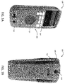
- FIGS. 1A and 1B provide front and back views of an exemplary system including a test and measurement tool and an imaging tool.
- the embodiment of FIGS. 1A and 1B includes a test and measurement tool 100 and an imaging tool 110 combined into a single combination tool 120.
- test and measurement tool 100 includes a back surface 102 through which the imaging tool 110 receives radiation from a target scene.
- imaging tool 110 can include a plurality of sensing components.
- imaging tool 110 may include one or both of an infrared (IR) camera and a visible light (VL) camera.
- IR infrared
- VL visible light
- various imaging tools such as 110 can include any combination of appropriate sensors capable of detecting a variety of wavelengths.
- imaging tool 110 is integrated into test and measurement tool 100. That is, the system of FIG. 1 shows a combination tool 120 having integral test and measurement tool 100 and imaging tool 110.
- Imaging tool 110 includes a camera capable of detecting radiation in one or more ranges of wavelengths. As described, imaging tool 110 may include a plurality of cameras for detecting radiation in different wavelength spectrums. In some examples, the imaging tool may include a plurality of sensor arrays, each sensor array sensitive to a different range of wavelengths. Some such embodiments include optics for separating light incident to imaging tool and substantially directing light within certain wavelength ranges to corresponding sensor arrays.
- the combination tool 120 of FIGS. 1A and 1B may be configured to generate image data and measurement data substantially simultaneously.
- combination tool 120 includes a display 108 capable of presenting one or more of image data, measurement data, or other information.
- any one or more of the test and measurement tool 100, imaging tool 110, and combination tool 120 can communicate one or more of measurement data, image data, or combined measurement and image data to any other system component.
- such data may be communicated to an external device, as described in U.S. Patent Application No. 14/855,989, filed September 16, 2015 , entitled "DISPLAY OF IMAGES FROM AN IMAGING TOOL EMBEDDED OR ATTACHED TO A TEST AND MEASUREMENT TOOL," now published as U.S. Patent Publication No. 2016/0076937 , which is assigned to the assignee of the instant application, and which is hereby incorporated by reference in its entirety.
- the tool 120 includes inputs 130, for example, for receiving one or more accessories (e.g., test leads).
- the one or more accessories can be used for interfacing with an object under test for generating measurement data representative of at least one parameter of a device under test.
- test and measurement tool 100 in combination tool 120 may perform a plurality of different measurement functions via inputs 130.
- the measurement function is selectable, for example, via a user interface 150.
- Interface 150 can include one or more elements by which a user can interact with the tool 120, such as a selection knob 152 or buttons 154, or other interface elements such as a touchscreen, switches, and the like.
- Combination tool 120 includes a display 108.
- Display 108 can be used to present various information to the user.
- display 108 can be configured to present measurement data generated by the test and measurement tool 100. Additionally or alternatively, the display 108 can be configured to present image data generated by imaging tool 110. In some embodiments, a combination of measurement data and image data can be presented on the display 108 for presentation to a user.
- FIG. 2 is an exemplary schematic diagram of a test and measurement tool comprising a variety of components.
- the test and measurement tool 200 may include one or power supplies 230 for providing electrical power to any of a variety of system components for performing a variety of tasks, such a performing one or more primary functions.
- the one or more power supplies 230 may include one or more batteries.
- the test and measurement tool 200 may be capable of running on AC power, e.g., from a standard wall receptacle. In some such embodiments, one or more batteries of the test and measurement tool 200 may be charged while the tool 200 is operating on or otherwise plugged into an AC power source.
- the test and measurement tool may include one or more inputs 220 configured to interface with an object under test for performing a measurement of a parameter thereof.
- the one or more inputs 220 may include any appropriate input for performing a measurement of a parameter of a device under test.
- the one or more inputs 220 may provide a signal indicative the parameter of the object under test to any combination of electronics 222 and a processor 224 for further processing of the signal.
- the test and measurement tool 200 includes a memory 226 for storing information indicative of one or more parameters of a device under test.
- processor 224 and memory 226 may be integrated into electronics 222.
- test and measurement tool 200 may include an interface 228 for interacting with a user.
- interface 228 may include one or more controls for receiving user inputs. Controls may include, for example, buttons, switches, knobs, touch screens, etc.
- a user may initiate a measurement or other test and measurement tool 200 function using controls.
- the interface may include a display for communicating information to a user. For example, the display may present a user with selectable options, such as various functions selectable by the user via controls. Additionally or alternatively, the display may be configured to present the results of one or more measurements performed by the test and measurement tool for observation by a user.
- a display is capable of presenting textual measurement information (e.g., letters, numbers, etc.), but is not capable of displaying image information, such as described elsewhere herein.
- power supply 230 is not capable of supporting a continuous image display without severely depleting the available power supply. Thus, in some examples, presentation of image data via interface 228 may be impossible or impractical.
- interface 228 may provide an interface with additional equipment.
- interface 228 can provide a communication interface between the test and measurement tool 200 and an imaging tool (e.g., 110) or an external device (e.g., smartphone, tablet, etc.).
- interface 228 can be used to export received measurement data, such as from inputs 220, or a processed result, for example, from processor 224.
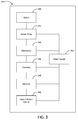
- FIG. 3 shows an example block diagram of an imaging tool configured for receiving electromagnetic radiation according to some exemplary systems.
- imaging tool 310 includes optics 340, a sensor array 342, electronics 344, one or more processors 346, memory units 348, input/output devices 350, and a power supply 352.
- the optics 340 can include optics for focusing, deflecting, and/or reflecting electromagnetic radiation from a target object onto the sensor array 342.
- the sensor array 342 may include an infrared sensor array sensitive to infrared radiation.
- An imaging tool including such an infrared sensor array may be used to make non-contact temperature measurements.
- the infrared sensor array 342 can include one or more thermal detectors such as microbolometers or thermopiles, or could be composed of photon detectors such as photodiodes or phototransistors, or other thermal or photon detection device.
- an infrared sensor array may include a single detector, for instance, for determining a spot temperature within a target scene.
- an infrared sensor array may comprise a plurality of such detectors for acquiring at least one of a spot temperature (e.g., via an average value of sensor array sensors) and a two-dimensional infrared image.
- the sensor array is fixed within the imaging tool 310 to provide a more durable device having fewer moving and moveable parts.
- the size and positioning of the detector depends on the characteristics of the optical system (e.g., the relationship between optics 340 and sensor array 342).
- the detector is generally circular having a diameter of 0.5 mm to 3 mm.
- detectors of any size and shape should be considered within the scope of the invention.
- the detector produces a signal as a function of the radiation or other scene data imaged thereupon. These signals can be processed by known methods to indicate a temperature or other metric indicated via the received radiation.
- the infrared sensor array 342 responds to infrared radiation ranging from approximately 0.7 microns to approximately 30 microns and can have a peak sensitivity within this range.
- the electronics 344 receive the output signals from the sensor array 342 and pass them to the processor 346 for analysis.
- the processor 346 can be used to run infrared thermometer applications including, but not limited to, deciding if the target object sufficiently fills the field of view, and averaging output signals for a period of time to reduce the impact of noisy measurements on the accuracy of the measured temperature.
- the processor 346 may be used to run corresponding imaging applications.
- Memory 348 can include but is not limited to, RAM, ROM, and any combination of volatile and non-volatile memory.
- a power supply 352 can include, but is not limited to, a battery, a parasitic energy system (e.g., an inductive system), and components for directly receiving AC power.
- the power supply 352 can provide power to the sensor array 342, electronics 344, processor 346, memory 348, and/or input/output devices 350.
- An input/output device 350 can include, but is not limited to, triggers to start and stop the image capture, visual displays, speakers, and communication devices that operate through wired or wireless communications.
- the input/output device 350 of the imaging tool 310 can include a display capable of displaying an image produced from data conveyed or captured by one or more sensor arrays 342.
- the display can be further configured to show other data, for instance, data from the test and measurement tool (e.g., via a communication port (not shown)) or other external sources.
- input/output device 350 may be capable of one or more of receiving measurement data from a measurement tool and communicating at least one of image data and received measurement data to an external device, such as a tablet, smartphone, computer, etc.
- a combination tool comprising a test and measurement tool and an imaging tool can include a processor capable of performing the processing functions of processor 224 and processor 346.
- a single memory in a combination tool can be capable of performing the functions of memory 226 and memory 348.
- such a combination tool can include a single power supply, interface, or the like.
- combination tools having both a test and measurement tool and an imaging tool can share any of a variety of components configured to interface with both the test and measurement tool and the imaging too.
- an imaging tool can be removably attached to a test and measurement tool to form a combination tool.
- the imaging tool and the test and measurement tool can include various components, such as a processor, memory, interface, display, and the like. Wired and/or wireless communication between the imaging tool and test and measurement tool can be used to communicate measurement data and/or image data between the tools.
- imaging tool and test and measurement tool can be in communication with an external device.
- the external device may include components such as memory, a processor, and/or a display.
- such components can be used in addition to similar components in the test and measurement tool and/or the imaging tool, or can replace the functionality of such components.
- image data and/or measurement data can be communicated to an external device for processing and/or display.
- a test and measurement tool may be capable of measuring high voltages. Accordingly, in some instances, such high voltages (or other potentially dangerous and/or damaging signals) may at times be present within circuitry (e.g., electronics 222) of the test and measurement tool. Standards and practices exist to protect users of typical test and measurement tools from being exposed to such high voltages. For example, one or both of solid state insulation and sufficient spacing between potentially high voltage portions of a test and measurement tool and location physically accessible to a user may provide protective electrical isolation to an operator.
- IEC 61010 standard for CAT III 1000V rated products requires approximately 16 millimeters spacing from components on which at high voltage could be present.
- IEC 61010 can require different spacing for different voltage ratings.
- the amount of spacing required can be reduced when solid materials (e.g., electrically insulating materials) are disposed between the potentially high voltage components and a user, such as an insulating casing of a test tool.
- an electrically insulating casing of a test tool provides sufficient insulation between a user and potentially high voltage components internal to the test tool.
- seams in the insulating casing are positioned that, even when tracing through the seams, the path length to any potentially high voltage component meets the required distance standard.
- an imaging tool when incorporated (e.g., built-in, removably attached, etc.) into a test and measurement tool capable of performing such high-voltage measurements, the imaging tool may provide a weak point in the protective insulating properties of the test and measurement tool.
- insulating casings used in test tools are often too opaque to allow radiation of desired wavelengths to pass therethrough. Accordingly, in some such embodiments, the imaging tool at least cannot be fully surrounded by such an insulating material.
- an imaging tool that is in close proximity with or in communication with a potentially high voltage portion of a test and measurement tool, or is in communication with a common component (e.g., a processor, memory, etc.), may include components at dangerously high voltages.
- an imaging tool can be recessed into a housing of the combination tool so that the distance between the imaging tool and the exterior of the tool meets any electrical isolation requirements.
- an imaging tool typically requires an opening in an insulating material to allow radiation to pass therethrough, for example, to reach one or more sensor arrays for generating image data.
- the combination tool can include an insulating casing including an opening to allow radiation to pass therethrough to reach a recessed imaging tool.
- an opening in the insulating casing of the combination tool to allow radiation to pass therethrough may also allow a user to access the internal imaging tool, for example, with their finger.
- Such portions of the combination tool and/or the imaging tool providing a shock risk for the user even though the imaging tool itself does not necessarily require dangerously high voltages for operation.
- the opening may be sized so as to reduce the likelihood of a user's accessing parts of the imaging tool.
- the opening is sized so that a user's finger is unlikely to reach to an unsafe distance from the imaging tool.
- the opening in the imaging tool can be sized so that a typical-sized finger from reaching unsafe internal portions of the combined tool.
- IEC International Electrotechnical Commission
- the opening can be configured so that such a "standard" finger, when inserted into the opening, is prevented from reaching a certain distance from any potentially high voltage components of the imaging tool.
- FIG. 4 shows a cross-sectional view of an exemplary imaging tool configured to reduce the risk of shocks from the imaging tool to the user.
- imaging tool 410 is embedded in a combination tool 400.
- the imaging tool 410 is surrounded by an insulating coating 420 of the combination tool 400.
- the insulating coating 420 includes an insulating material (shown in a crosshatch pattern) having sufficient thickness to provide proper electrical isolation between the imaging tool 410 and a user handling the combination tool 400.
- the shape of the insulating coating is exemplary, and that many appropriate shapes are possible.
- the combination tool 400 includes a housing substantially surrounding the insulating coating 420 to provide a convenient shape for holding by the user.
- the housing comprises insulating coating 420.
- the imaging tool 410 includes a receiving end 412 configured to receive electromagnetic radiation and to direct the received radiation to an imaging element such as a sensor array.
- the receiving end can include, for example, one or more lenses, filters, windows, or the like.
- the insulating coating 420 includes an opening 424 proximate the receiving end 412 of the imaging tool 410 for allowing electromagnetic radiation to pass therethrough and reach the receiving end 412 of the imaging tool 410.
- the opening 424 is shaped to limit the depth of penetration of the tip 432 of a finger 430 (e.g., a standard finger as defined by the IEC) into the opening.
- the opening 424 is angled so that the tip 432 of the finger 430 cannot get within a distance D 1 of the closest end (e.g., receiving end 412) of the imaging tool 410.
- the distance D 1 is a minimum distance required to provide adequate isolation between the imaging tool 410 and the tip 432 of a finger 430 inserted as far into the opening 424 as possible.
- the distance D 1 may depend on a variety of factors, such as one or more of the maximum voltage expected to be present or possibly present at the imaging tool 410, materials disposed between the imaging tool 410 and the tip 432 of finger 430, the standard of safety being applied (e.g., IEC standards), and the like.
- the test and measurement tool of the combination tool 400 is capable of receiving voltages up to 1000V, and that the imaging tool 410 may similarly reach approximately 1000V relative to earth ground in some instances. Applying 1000V CAT III isolation according to IEC standards, distance D 1 may be approximately 16 millimeters (mm).
- opening 424 may be sized/shaped so that the tip 432 of a standard finger 430 (i.e., a finger size/shape according to a standard such as the IEC) cannot come within 16 millimeters of the imaging tool 410 when fully inserted into the opening 424.
- a minimum value for the distance D 1 is dictated by safety standards.
- the distance D 1 is based on IEC 61010 safety standards.
- the actual distance D 1 can be dependent on the voltage rating of the tool combined with the IEC 61010 standard. That is, for example, a tool rated at fewer than 1000V may allow spacing that is less than 16 millimeters.
- imaging tool 410 may include a narrow field of view (e.g., via a lens or other optics) so that the insulating coating 420 proximate the opening 424 does not significantly block part of the field of view of the imaging tool 410.
- a narrow field of view e.g., via a lens or other optics
- the diagram of FIG. 4 is exemplary and is intended to show the implementation of one or more design options. Unless otherwise stated, elements shown in FIG. 4 , or other figures herein, are not necessarily drawn to scale or intended to show exact dimensions or configurations.
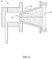
- FIG. 5 shows a cross-sectional view of an alternative exemplary imaging tool in a combination tool configured to reduce the risk of shocks from the imaging tool to the user.
- combination tool 500 includes an imaging tool 510 embedded therein.
- the imaging tool 510 is embedded in an insulating coating 520 of the combination tool 500.
- the insulating coating 520 includes an insulating material (shown in a crosshatch pattern) having sufficient thickness to provide proper electrical isolation between the imaging tool 510 and a user handling the combination tool 500.
- the combination tool 500 can include a housing surrounding the insulating coating 520 and shaped for convenient grasping by a user. Additionally or alternatively, such a housing can include the insulating coating 520.
- the imaging tool 510 includes a receiving end 512 configured to receive electromagnetic radiation and to direct the received radiation to an imaging element such as a sensor array.
- the receiving end 512 can include one or more lenses, filters, windows, or combinations thereof. In some examples, receiving end need not include any additional components. Additionally or alternatively, the receiving end can include the imaging element, such as a sensor array.
- the insulating coating 520 includes an opening 524 proximate the receiving end 512 of the imaging tool for allowing electromagnetic radiation to pass therethrough and reach the receiving end 512 of the imaging tool 510.
- the opening 524 is covered at a distal end by a window 530.
- window 530 can effectively prevent a user from inserting an object (e.g., a finger) into the opening 524 and toward a potentially high voltage component of imaging tool 510.
- the window 530 may be bonded or molded to the insulating coating 520 or other component, such as a housing surrounding the imaging tool 510.
- the window 530 is rigidly secured over the opening 524 to deter objects from entering the opening 524 and potentially encountering the imaging tool 510.
- the user is protected from high voltage inside the tool 500 by construction providing sufficient spacing and/or sufficiently insulative materials, including through all seams and edges including around the window 530.
- the window 530 is optically transmissive in one or more spectral regions detectable by the imaging tool 510, allowing the imaging tool 510 to receive radiation through the window 530.
- an imaging tool e.g., 510
- the imaging tool 510 can receive radiation in such spectral regions from a target scene and generate corresponding image data.
- the imaging tool 510 can be capable of generating image data from different spectral regions, such as separate infrared image data and visible light image data.
- Window 530 may be made of a material capable of effectively transmitting wavelengths of radiation detectable by a sensor array of the imaging tool 510, such as infrared and/or visible light radiation.
- window 530 can include an infrared-transmissive material, such as germanium.
- the window 530 is positioned a distance D 2 from the receiving end 512 of the imaging tool 510.
- the distance D 2 may be determined based on a minimum distance to meet a certain isolation standard, such as a 1000V CAT III isolation standard, to provide sufficient electrical isolation between a user and the imaging tool 510. Additionally or alternatively, the distance D 2 can depend on the material of window 530. For example, if window 530 comprises a substantially electrically insulating material, the distance D 2 required to provide sufficient isolation may be less than if the window 530 comprises an electrically conductive material. In some embodiments, the window does not provide sufficient insulation to protect a user from a high voltage at the imaging tool 510.
- distance D 2 may be at least the distance required to provide sufficient electrical isolation between a user and the imaging tool 510 without a window present (e.g., similar to the distance D 1 in FIG. 4 ). More insulating materials used as window 530 may allow a shorter distance to provide similarly effective isolation. That is, in some examples, an electrically insulating window 530 may provide additional protection to a user so that the minimum safe distance for a user of the tool 500 of FIG. 5 can be less than that for a user of tool 400 of FIG. 4 .
- window 530 is at least partially electrically insulating
- imaging tools 410 and 510 of FIGS. 4 and 5 respectively, can be operated with reduced risk of shock to an operator, wherein D 2 and D 1 are minimum safe operating distances and D 2 ⁇ D 1 .
- window 530 may prevent a user from inserting an object (e.g., a finger) into the opening 524.
- an object e.g., a finger
- a user may be sufficiently protected from the imaging tool 510 without restriction on the size or shape of the opening 524.
- the imaging tool 510 comprises an infrared camera module sensitive to infrared radiation and capable of generating infrared radiation.
- the thermal profile of the window 530 may lead to errors in generated infrared image data. That is, infrared radiation from the window 530 can be detected by the imaging tool and undesirably be incorporated into generated thermal image data.
- portions of the electrically insulating coating 520 may comprise a thermally conductive material.
- a thermally conductive material may place the imaging tool 510 and the window 530 in substantial thermal equilibrium and reduce errors in infrared image data due to window temperature offsets.
- portions of one or both of the imaging tool 510 and the window 530 can be thermally isolated from other system components, particularly those which may act as heat sources to alter the temperature of the imaging tool 510 or window 530.
- thermally isolating materials may be placed between one or both of the imaging tool 510 and the window 530 and a power source or other powered component that may generate heat.
- FIGS. 4 and 5 show exemplary methods for embedding an imaging tool into a test and measurement tool so that, if the imaging tool is at high voltage, a user is substantially protected from electrical shock from the imaging tool and test and measurement tool.
- an embedded imaging tool can be fixedly integrated with a test and measurement tool to form a single combination tool.
- a modular combination tool can include an imaging tool that may be removably attached to the test and measurement tool.
- the test and measurement tool may be configured to receive the imaging tool such that, once combined with the test and measurement tool, any potentially high voltage portions of the imaging tool are electrically isolated from a user.
- FIG. 4 and 5 are illustrative in nature. Components in FIGS. 4 and 5 are not necessarily drawn to scale unless otherwise specified. While certain aspects of the figures (e.g., distances D 1 , D 2 ) may be shown as meeting certain standards (e.g., IEC 61010 standards), such aspects can be achieved in a variety of ways. Additionally or alternatively, the shapes and sizes of other portions of the tool (e.g., the shape and/or size of the insulating coating surrounding the imaging tool, the imaging tool itself, etc.) may vary without departing from the scope of the disclosure.
- standards e.g., IEC 61010 standards
- FIGS. 4 and 5 provide electrical isolation between a user and the imaging tool by embedding the imaging tool within electrical isolation (e.g., insulating coating), other ways of safely operating an imaging tool communicating with a test and measurement tool are possible, such as described, for example, in U.S. Provisional Application No. 62/219,415 , which is incorporated herein by reference, and U.S. Patent Application No. 15/262,820, filed September 12, 2016 , and entitled "ELECTRICAL ISOLATION FOR A CAMERA IN A TEST AND MEASUREMENT TOOL," which is assigned to the assignee of the instant application, and is incorporated herein by reference in its entirety.
- electrical isolation e.g., insulating coating
- the imaging tool may itself be electrically isolated from portions of the test and measurement tool. In such embodiments, even if portions of the test and measurement tool are at a high voltage, the imaging tool may remain safe to the touch and need not be isolated from a user.
- Examples provide an analysis system comprising a test and measurement tool, comprising a test and measurement circuit configured to interface with a device under test and to generate measurement data representative of at least one parameter of the device under test, an imaging tool attached to the test and measurement tool and configured to receive electromagnetic radiation from a target scene and to generate image data representative of the target scene, a housing enclosing the test and measurement tool and the imaging tool, the housing comprising an aperture for permitting electromagnetic radiation to enter the housing so that the imaging tool receives the electromagnetic radiation, a processor in communication with the test and measurement circuit of the test and measurement tool and the imaging tool and configured to receive and process measurement data and image data, and at least one electrical isolation mechanism configured and arranged so that a user operating the analysis tool is electrically isolated from the test and measurement circuit through the imaging tool.
- the at least one electrical isolation mechanism comprises an insulating coating surrounding at least a portion of the imaging tool and having an opening proximate the imaging tool such that electromagnetic radiation can enter the opening and reach the imaging tool.
- the opening in the insulating coating is sized so that a standard finger cannot penetrate the opening to within a predetermined distance of the imaging tool.
- the standard finger and the predetermined distance meet IEC 61010 standards.
- Some examples further comprise a window substantially covering the opening in the insulating coating proximate the imaging tool.
- the window is positioned at least a first distance from the imaging tool.
- the first distance is dependent on electrical characteristics of the window and a voltage rating of the test and measurement circuit.
- the imaging tool comprises an infrared camera module, and wherein the window comprises an infrared-transmissive material.
- the imaging tool further comprises a visible light camera module, and wherein the window is substantially transparent to visible light.
- the window is in thermal communication with a thermally conductive portion of the electrically isolating material.
- the imaging tool is removably attached to the test and measurement tool.
- Examples provide an analysis system comprising a test and measurement tool, comprising a test and measurement circuit configured to interface with a device under test and to generate measurement data representative of at least one parameter of the device under test, an imaging tool attached to the test and measurement tool and configured to receive electromagnetic radiation from a target scene via a receiving end of the imaging tool and to generate image data representative of the target scene, the imaging tool being electrically coupleable to the test and measurement circuit of the test and measurement tool, and a housing comprising an insulating material at least partially surrounding the imaging tool, the insulating material having an aperture proximate the receiving end of the imaging tool and the housing being configured to prevent a user from accessing a portion of the imaging device within the housing.
- the imaging tool is fixedly attached to the test and measurement tool.
- the housing comprises an opening shaped and sized to prevent a standard finger from reaching within a predetermined distance of the receiving end of the imaging tool.
- the opening is frustoconical in shape.
- the imaging tool comprises a wide angle lens.
- Some examples further comprise a window positioned to prevent access to the imaging tool via the opening, and wherein the housing is configured to support the window in place over the opening.
- the portion of the housing supporting the window comprises an electrically insulating and thermally conductive material.
- the imaging tool comprises an infrared camera module, and wherein the window is substantially transparent to infrared radiation.
- the test and measurement tool comprises a digital multimeter.
- Examples provide a combination tool comprising a test and measurement circuit configured to interface with a device under test in order to measure at least one electrical parameter of the device under test, an imaging tool fixedly attached to and in electrical communication with the test and measurement tool, the imaging tool being configured to generate image data representative of a target scene, and a housing comprising an insulating material and surrounding at least a portion of the test and measurement circuit and the imaging tool, the housing having an opening proximate the imaging tool so that electromagnetic radiation from the target scene travels through the opening in the housing and is received by the imaging tool, wherein the housing is configured to prevent a standard sized finger from accessing the imaging tool within the housing.
- the housing is configured to support a window over the opening in order to prevent the standard sized finger from accessing a position within a predetermined distance from the imaging tool via the opening, the predetermined distance depending on the electrical characteristics of the window.
- the opening is frustoconical in shape and is sized so that a finger inserted into the housing cannot within a predetermined distance from the imaging tool via the opening, and wherein the predetermined distance depends on a voltage rating of the test and measurement circuit.
Landscapes
- Physics & Mathematics (AREA)
- General Physics & Mathematics (AREA)
- Engineering & Computer Science (AREA)
- Multimedia (AREA)
- Signal Processing (AREA)
- Spectroscopy & Molecular Physics (AREA)
- Health & Medical Sciences (AREA)
- Toxicology (AREA)
- Radiation Pyrometers (AREA)
- Photometry And Measurement Of Optical Pulse Characteristics (AREA)
- Length Measuring Devices By Optical Means (AREA)
- Analysing Materials By The Use Of Radiation (AREA)
Abstract
Description
- This application claims the benefit of
U.S. Provisional Application No. 62/219,415, filed September 16, 2015 - This disclosure generally relates to electrical test tools capable of withstanding high voltages and associated imaging tools.
- Various information regarding parameters of system components may be useful in analyzing individual component's performance, operating conditions, lifespan, and other various aspects. Some such information includes measureable quantities, such as a current, voltage, power, impedance, vibration, and the like. Analysis of components of a system may provide insight into ways the system may be improved, for example, by repairing or replacing faulty or otherwise non-optimal components. Various test and measurement tools are capable of performing such measurements, and are often used in analyzing such components.
- In some instances, when analyzing electrical equipment, dangerously high voltages may at times be present in various parts of the circuit in the analysis instrument. Standards and practices exist to protect users from being exposed to these voltages, such as solid insulation between any potentially high voltage portions and the user.
- In some examples, additional information may be helpful in analyzing such components. For example, imaging techniques, such as infrared imaging, may provide useful additional information. Infrared imagery of a system or components thereof can provide thermal patterns of the scene, highlighting temperature abnormalities in system components. Such imagery may be useful in diagnosing similar or different issues that may be detected or otherwise analyzed using standard test and measurement tools as discussed above.
- Since the advent of thermal imaging applications in electrical environments, there has been a need to keep the operator at a safe distance from the electrical circuits under observation. In some situations, companies have developed optical windows for switch gear cabinets, enabling physical isolation from the high voltage, but allowing optical measurements.
- In the event that a user is performing both imaging and other analysis (e.g., electrical measurement analysis), instances may occur in which the imaging apparatus is exposed to or proximate potentially high voltage environments. Thus, additional safety measures may be necessary for protecting the user from exposure to potentially dangerous signals via the imaging apparatus.
- Aspects of this disclosure are directed toward systems and methods for providing combined test and measurement analysis and imaging analysis while providing adequate safety to a user. Embodiments in this disclosure include systems comprising a test and measurement tool comprising a test and measurement circuit and being configured to generate measurement data representative of at least one parameter of an object under test. A system can further include an imaging tool configured to generate image data representative of a target scene. In various embodiments, the imaging tool can include an infrared (IR) imaging tool and/or a visible light (VL) imaging tool.
- Exemplary systems can include a housing enclosing the test and measurement tool and the imaging tool and can include an aperture permitting electromagnetic radiation to enter the housing so that the imaging tool receives the electromagnetic radiation. The system can include at least one electrical isolation mechanism configured and arranged so that a user operating the analysis tool is electrically isolated from the test and measurement circuit through the imaging tool.
- In some examples, the electrical isolation mechanism includes an insulating coating surrounding at least a portion of the imaging tool and having an opening proximate the imaging tool. In some such examples, electromagnetic radiation can enter the opening and reach the imaging tool. However, in some embodiments, the opening in the insulating coating is sized so that a standard finger cannot penetrate the opening to within a predetermined distance of the imaging tool.
- In some examples, the standard finger and the predetermined distance meet IEC 61010 standards. For instance in some embodiments, the opening prevents an object of standard dimensions (e.g., as defined by the IEC) from reaching within the predetermined distance of the imaging tool. The predetermined distance can be based, for example, on a maximum voltage rating of the test and measurement circuit.
- Additionally or alternatively, in some examples, the system includes a window substantially covering the opening in the coating. The window can prevent the user (e.g., the finger of a user) from entering the housing and coming within a predetermined distance of the imaging tool. In some such embodiments, the window can provide electrically insulating properties to at least partially protect the user from electrical shocks from the imaging tool. Thus, in some such examples, the predetermined distance in embodiments including such a window can be less than the predetermined distance in embodiments not including the window.
- The details of one or more examples are set forth in the accompanying drawings and the description below. Other features, objects, and advantages will be apparent from the description and drawings, and from the claims.
-
-
FIGS. 1A and 1B provide front and back views of an exemplary system including a test and measurement tool and an imaging tool. -
FIG. 2 is an exemplary schematic diagram of a test and measurement tool comprising a variety of components. -
FIG. 3 shows an example block diagram of an imaging tool configured for receiving electromagnetic radiation according to some exemplary systems. -
FIG. 4 shows a cross-sectional view of an exemplary imaging tool configured to reduce the risk of shocks from the imaging tool to the user. -
FIG. 5 shows a cross-sectional view of an alternative exemplary imaging tool in a combination tool configured to reduce the risk of shocks from the imaging tool to the user. - Aspects of the disclosure generally relate to systems and methods providing electrical isolation for user safety in combination imaging and test and measurement tools. Test and measurement tools can be generally capable of determining at least one parameter of a device under test. Exemplary test and measurement tools can include, but are not limited to, digital multimeters, current measurement tools, power quality tools, vibration tools, portable oscilloscope tools, laser alignment tools, ultrasonic test tools, insulation resistance testers, multi-function electrical test tools, single-function electrical test tools, contact temperature measurement tools, humidity measurement tools, air-flow measurement tools, air temperature measurement tools , air quality and particulate measurement tools, and the like. In some embodiments, one or more such test and measurement tools can produce and/or measure an electrical signal that is unsafe for the operator of the test and measurement tool without proper protection.
- One or more imaging devices can be integrated with or otherwise attached or attachable to a test and measurement tool such as described in
U.S. Patent Application No. 14/855,884 entitled "TEST AND MEASUREMENT SYSTEM WITH REMOVABLE IMAGING TOOL," now published asU.S. Patent Publication No. 2016/0080666 , orU.S. Patent Application No. 14,855/844 U.S. Patent Publication No. 2016/0076936 , each of which was filed September 16, 2015, is assigned to the assignee of the instant application, and is hereby incorporated by reference in its entirety. In various examples, the imaging tool interfacing with a test and measurement tool can be sensitive to any of a variety of wavelengths. Exemplary imaging components can include sensors which can detect visible, near infrared (NIR), short-wavelength infrared (SWIR), long wavelength infrared (LWIR), terahertz (THz), ultraviolet (UV), X-Ray or other wavelengths. In some embodiments, the imaging component can include one or more imaging sensors, for example, infrared (IR) and visible light (VL) cameras. -
FIGS. 1A and 1B provide front and back views of an exemplary system including a test and measurement tool and an imaging tool. The embodiment ofFIGS. 1A and 1B includes a test andmeasurement tool 100 and animaging tool 110 combined into asingle combination tool 120. In the illustrated embodiment, test andmeasurement tool 100 includes aback surface 102 through which theimaging tool 110 receives radiation from a target scene. - In some examples,
imaging tool 110 can include a plurality of sensing components. For example,imaging tool 110 may include one or both of an infrared (IR) camera and a visible light (VL) camera. It will be appreciated that various imaging tools such as 110 can include any combination of appropriate sensors capable of detecting a variety of wavelengths. - In the example of
FIGS. 1A and 1B ,imaging tool 110 is integrated into test andmeasurement tool 100. That is, the system ofFIG. 1 shows acombination tool 120 having integral test andmeasurement tool 100 andimaging tool 110.Imaging tool 110 includes a camera capable of detecting radiation in one or more ranges of wavelengths. As described,imaging tool 110 may include a plurality of cameras for detecting radiation in different wavelength spectrums. In some examples, the imaging tool may include a plurality of sensor arrays, each sensor array sensitive to a different range of wavelengths. Some such embodiments include optics for separating light incident to imaging tool and substantially directing light within certain wavelength ranges to corresponding sensor arrays. - The
combination tool 120 ofFIGS. 1A and 1B may be configured to generate image data and measurement data substantially simultaneously. In some examples,combination tool 120 includes a display 108 capable of presenting one or more of image data, measurement data, or other information. Additionally or alternatively, any one or more of the test andmeasurement tool 100,imaging tool 110, andcombination tool 120 can communicate one or more of measurement data, image data, or combined measurement and image data to any other system component. In some examples, such data may be communicated to an external device, as described inU.S. Patent Application No. 14/855,989, filed September 16, 2015 U.S. Patent Publication No. 2016/0076937 , which is assigned to the assignee of the instant application, and which is hereby incorporated by reference in its entirety. - In the front view of
FIG. 1A , thetool 120 includesinputs 130, for example, for receiving one or more accessories (e.g., test leads). The one or more accessories can be used for interfacing with an object under test for generating measurement data representative of at least one parameter of a device under test. In some embodiments, test andmeasurement tool 100 incombination tool 120 may perform a plurality of different measurement functions viainputs 130. In some embodiments, the measurement function is selectable, for example, via a user interface 150. Interface 150 can include one or more elements by which a user can interact with thetool 120, such as aselection knob 152 orbuttons 154, or other interface elements such as a touchscreen, switches, and the like. -
Combination tool 120 includes a display 108. Display 108 can be used to present various information to the user. In some examples, display 108 can be configured to present measurement data generated by the test andmeasurement tool 100. Additionally or alternatively, the display 108 can be configured to present image data generated byimaging tool 110. In some embodiments, a combination of measurement data and image data can be presented on the display 108 for presentation to a user. -
FIG. 2 is an exemplary schematic diagram of a test and measurement tool comprising a variety of components. In the illustrated example, the test andmeasurement tool 200 may include one orpower supplies 230 for providing electrical power to any of a variety of system components for performing a variety of tasks, such a performing one or more primary functions. In some embodiments, the one ormore power supplies 230 may include one or more batteries. Additionally or alternatively, the test andmeasurement tool 200 may be capable of running on AC power, e.g., from a standard wall receptacle. In some such embodiments, one or more batteries of the test andmeasurement tool 200 may be charged while thetool 200 is operating on or otherwise plugged into an AC power source. - The test and measurement tool may include one or
more inputs 220 configured to interface with an object under test for performing a measurement of a parameter thereof. In various examples, the one ormore inputs 220 may include any appropriate input for performing a measurement of a parameter of a device under test. The one ormore inputs 220 may provide a signal indicative the parameter of the object under test to any combination ofelectronics 222 and aprocessor 224 for further processing of the signal. In some examples, the test andmeasurement tool 200 includes amemory 226 for storing information indicative of one or more parameters of a device under test. In some embodiments, one or both ofprocessor 224 andmemory 226 may be integrated intoelectronics 222. - In some embodiments, test and
measurement tool 200 may include aninterface 228 for interacting with a user. In some examples,interface 228 may include one or more controls for receiving user inputs. Controls may include, for example, buttons, switches, knobs, touch screens, etc. In some embodiments, a user may initiate a measurement or other test andmeasurement tool 200 function using controls. Additionally or alternatively, the interface may include a display for communicating information to a user. For example, the display may present a user with selectable options, such as various functions selectable by the user via controls. Additionally or alternatively, the display may be configured to present the results of one or more measurements performed by the test and measurement tool for observation by a user. In some examples, a display is capable of presenting textual measurement information (e.g., letters, numbers, etc.), but is not capable of displaying image information, such as described elsewhere herein. Additionally or alternatively, in some embodiments,power supply 230 is not capable of supporting a continuous image display without severely depleting the available power supply. Thus, in some examples, presentation of image data viainterface 228 may be impossible or impractical. - In some examples,
interface 228 may provide an interface with additional equipment. For example, in some embodiments,interface 228 can provide a communication interface between the test andmeasurement tool 200 and an imaging tool (e.g., 110) or an external device (e.g., smartphone, tablet, etc.). In various embodiments,interface 228 can be used to export received measurement data, such as frominputs 220, or a processed result, for example, fromprocessor 224. -
FIG. 3 shows an example block diagram of an imaging tool configured for receiving electromagnetic radiation according to some exemplary systems. In the illustrated embodiment,imaging tool 310 includesoptics 340, asensor array 342,electronics 344, one ormore processors 346,memory units 348, input/output devices 350, and apower supply 352. - The
optics 340 can include optics for focusing, deflecting, and/or reflecting electromagnetic radiation from a target object onto thesensor array 342. In some examples, thesensor array 342 may include an infrared sensor array sensitive to infrared radiation. An imaging tool including such an infrared sensor array may be used to make non-contact temperature measurements. - In such embodiments, the
infrared sensor array 342 can include one or more thermal detectors such as microbolometers or thermopiles, or could be composed of photon detectors such as photodiodes or phototransistors, or other thermal or photon detection device. In some examples, an infrared sensor array may include a single detector, for instance, for determining a spot temperature within a target scene. Alternatively, an infrared sensor array may comprise a plurality of such detectors for acquiring at least one of a spot temperature (e.g., via an average value of sensor array sensors) and a two-dimensional infrared image. - One having ordinary skill in the art will recognize that various sensor arrays (e.g. photon sensor arrays) can be used, and can be used in combination with one or more infrared sensor arrays. In some examples, the sensor array is fixed within the
imaging tool 310 to provide a more durable device having fewer moving and moveable parts. In various examples, the size and positioning of the detector depends on the characteristics of the optical system (e.g., the relationship betweenoptics 340 and sensor array 342). In some embodiments, the detector is generally circular having a diameter of 0.5 mm to 3 mm. However detectors of any size and shape should be considered within the scope of the invention. The detector produces a signal as a function of the radiation or other scene data imaged thereupon. These signals can be processed by known methods to indicate a temperature or other metric indicated via the received radiation. - A person having ordinary skill in the art will recognize that many materials and materials technologies may be suitable for use in an infrared sensor array. In some examples, the
infrared sensor array 342 responds to infrared radiation ranging from approximately 0.7 microns to approximately 30 microns and can have a peak sensitivity within this range. Theelectronics 344 receive the output signals from thesensor array 342 and pass them to theprocessor 346 for analysis. - When an infrared sensor assembly is used, the
processor 346 can be used to run infrared thermometer applications including, but not limited to, deciding if the target object sufficiently fills the field of view, and averaging output signals for a period of time to reduce the impact of noisy measurements on the accuracy of the measured temperature. In the case of alternative sensor arrays (e.g., sensitive to one or more of visible light, ultraviolet light, X-rays, etc.), theprocessor 346 may be used to run corresponding imaging applications. -
Memory 348 can include but is not limited to, RAM, ROM, and any combination of volatile and non-volatile memory. Apower supply 352 can include, but is not limited to, a battery, a parasitic energy system (e.g., an inductive system), and components for directly receiving AC power. Thepower supply 352 can provide power to thesensor array 342,electronics 344,processor 346,memory 348, and/or input/output devices 350. An input/output device 350 can include, but is not limited to, triggers to start and stop the image capture, visual displays, speakers, and communication devices that operate through wired or wireless communications. - For instance, in some examples, the input/
output device 350 of theimaging tool 310 can include a display capable of displaying an image produced from data conveyed or captured by one ormore sensor arrays 342. In some examples, the display can be further configured to show other data, for instance, data from the test and measurement tool (e.g., via a communication port (not shown)) or other external sources. Additionally or alternatively, input/output device 350 may be capable of one or more of receiving measurement data from a measurement tool and communicating at least one of image data and received measurement data to an external device, such as a tablet, smartphone, computer, etc. - In some embodiments, the functionality of one or more components of one or both of the test and
measurement tool 200 orimaging tool 310 can be shared between the components. For example, in some embodiments, a combination tool comprising a test and measurement tool and an imaging tool can include a processor capable of performing the processing functions ofprocessor 224 andprocessor 346. Additionally or alternatively, a single memory in a combination tool can be capable of performing the functions ofmemory 226 andmemory 348. Similarly, such a combination tool can include a single power supply, interface, or the like. In general, combination tools having both a test and measurement tool and an imaging tool can share any of a variety of components configured to interface with both the test and measurement tool and the imaging too. - As described elsewhere herein, in some examples, an imaging tool can be removably attached to a test and measurement tool to form a combination tool. In some such examples, one or both of the imaging tool and the test and measurement tool can include various components, such as a processor, memory, interface, display, and the like. Wired and/or wireless communication between the imaging tool and test and measurement tool can be used to communicate measurement data and/or image data between the tools. Several such configurations are described in
U.S. Patent Application No. 14/855,884 , entitled "TEST AND MEASUREMENT SYSTEM WITH REMOVABLE IMAGING TOOL," now published asU.S. Patent Publication No. 2016/0080666 , which is incorporated by reference. Similarly, one or both of imaging tool and test and measurement tool can be in communication with an external device. The external device may include components such as memory, a processor, and/or a display. In various embodiments, such components can be used in addition to similar components in the test and measurement tool and/or the imaging tool, or can replace the functionality of such components. For instance, in some examples, image data and/or measurement data can be communicated to an external device for processing and/or display. Some such configurations are described inU.S. Patent Application No. 14/855,989, filed September 16, 2015 U.S. Patent Publication No. 2016/0076937 , which is incorporated by reference. - In some embodiments, a test and measurement tool may be capable of measuring high voltages. Accordingly, in some instances, such high voltages (or other potentially dangerous and/or damaging signals) may at times be present within circuitry (e.g., electronics 222) of the test and measurement tool. Standards and practices exist to protect users of typical test and measurement tools from being exposed to such high voltages. For example, one or both of solid state insulation and sufficient spacing between potentially high voltage portions of a test and measurement tool and location physically accessible to a user may provide protective electrical isolation to an operator.
- For example, IEC 61010 standard for CAT III 1000V rated products requires approximately 16 millimeters spacing from components on which at high voltage could be present. Similarly, IEC 61010 can require different spacing for different voltage ratings. In some examples, the amount of spacing required can be reduced when solid materials (e.g., electrically insulating materials) are disposed between the potentially high voltage components and a user, such as an insulating casing of a test tool. In some examples, an electrically insulating casing of a test tool provides sufficient insulation between a user and potentially high voltage components internal to the test tool. In some embodiments, seams in the insulating casing are positioned that, even when tracing through the seams, the path length to any potentially high voltage component meets the required distance standard.
- However, when an imaging tool is incorporated (e.g., built-in, removably attached, etc.) into a test and measurement tool capable of performing such high-voltage measurements, the imaging tool may provide a weak point in the protective insulating properties of the test and measurement tool. For example, insulating casings used in test tools are often too opaque to allow radiation of desired wavelengths to pass therethrough. Accordingly, in some such embodiments, the imaging tool at least cannot be fully surrounded by such an insulating material. Thus, an imaging tool that is in close proximity with or in communication with a potentially high voltage portion of a test and measurement tool, or is in communication with a common component (e.g., a processor, memory, etc.), may include components at dangerously high voltages.
- In some configurations of a combination tool such as shown in
FIGS. 1A and 1B , an imaging tool can be recessed into a housing of the combination tool so that the distance between the imaging tool and the exterior of the tool meets any electrical isolation requirements. As described, an imaging tool typically requires an opening in an insulating material to allow radiation to pass therethrough, for example, to reach one or more sensor arrays for generating image data. Thus, the combination tool can include an insulating casing including an opening to allow radiation to pass therethrough to reach a recessed imaging tool. - However, an opening in the insulating casing of the combination tool to allow radiation to pass therethrough may also allow a user to access the internal imaging tool, for example, with their finger. Such portions of the combination tool and/or the imaging tool providing a shock risk for the user even though the imaging tool itself does not necessarily require dangerously high voltages for operation.
- In some embodiments, to minimize the risk of a user accessing a potentially high-voltage imaging tool, the opening may be sized so as to reduce the likelihood of a user's accessing parts of the imaging tool. For instance, in some embodiments, the opening is sized so that a user's finger is unlikely to reach to an unsafe distance from the imaging tool. For instance, in some examples, the opening in the imaging tool can be sized so that a typical-sized finger from reaching unsafe internal portions of the combined tool. For example, the International Electrotechnical Commission (IEC) provides dimensions for finger-sized probes in order to approximate the depth a finger may penetrate a structure. The opening can be configured so that such a "standard" finger, when inserted into the opening, is prevented from reaching a certain distance from any potentially high voltage components of the imaging tool.
-
FIG. 4 shows a cross-sectional view of an exemplary imaging tool configured to reduce the risk of shocks from the imaging tool to the user. In the illustrated example,imaging tool 410 is embedded in acombination tool 400. Theimaging tool 410 is surrounded by an insulatingcoating 420 of thecombination tool 400. The insulatingcoating 420 includes an insulating material (shown in a crosshatch pattern) having sufficient thickness to provide proper electrical isolation between theimaging tool 410 and a user handling thecombination tool 400. It will be appreciated that the shape of the insulating coating is exemplary, and that many appropriate shapes are possible. In some embodiments, thecombination tool 400 includes a housing substantially surrounding the insulatingcoating 420 to provide a convenient shape for holding by the user. In some such embodiments, the housing comprises insulatingcoating 420. - In the illustrated embodiment, the
imaging tool 410 includes a receivingend 412 configured to receive electromagnetic radiation and to direct the received radiation to an imaging element such as a sensor array. The receiving end can include, for example, one or more lenses, filters, windows, or the like. The insulatingcoating 420 includes anopening 424 proximate the receivingend 412 of theimaging tool 410 for allowing electromagnetic radiation to pass therethrough and reach the receivingend 412 of theimaging tool 410. - In the illustrated embodiment, the
opening 424 is shaped to limit the depth of penetration of thetip 432 of a finger 430 (e.g., a standard finger as defined by the IEC) into the opening. For example, in some configurations theopening 424 is angled so that thetip 432 of thefinger 430 cannot get within a distance D1 of the closest end (e.g., receiving end 412) of theimaging tool 410. In some examples, the distance D1 is a minimum distance required to provide adequate isolation between theimaging tool 410 and thetip 432 of afinger 430 inserted as far into theopening 424 as possible. - The distance D1 may depend on a variety of factors, such as one or more of the maximum voltage expected to be present or possibly present at the
imaging tool 410, materials disposed between theimaging tool 410 and thetip 432 offinger 430, the standard of safety being applied (e.g., IEC standards), and the like. In an exemplary embodiment, the test and measurement tool of thecombination tool 400 is capable of receiving voltages up to 1000V, and that theimaging tool 410 may similarly reach approximately 1000V relative to earth ground in some instances. Applying 1000V CAT III isolation according to IEC standards, distance D1 may be approximately 16 millimeters (mm). That is, opening 424 may be sized/shaped so that thetip 432 of a standard finger 430 (i.e., a finger size/shape according to a standard such as the IEC) cannot come within 16 millimeters of theimaging tool 410 when fully inserted into theopening 424. In some examples, a minimum value for the distance D1 is dictated by safety standards. For instance, in some embodiments, the distance D1 is based on IEC 61010 safety standards. In some such examples, the actual distance D1 can be dependent on the voltage rating of the tool combined with the IEC 61010 standard. That is, for example, a tool rated at fewer than 1000V may allow spacing that is less than 16 millimeters. - In various embodiments,
imaging tool 410 may include a narrow field of view (e.g., via a lens or other optics) so that the insulatingcoating 420 proximate theopening 424 does not significantly block part of the field of view of theimaging tool 410. It will be appreciated that the diagram ofFIG. 4 is exemplary and is intended to show the implementation of one or more design options. Unless otherwise stated, elements shown inFIG. 4 , or other figures herein, are not necessarily drawn to scale or intended to show exact dimensions or configurations. -
FIG. 5 shows a cross-sectional view of an alternative exemplary imaging tool in a combination tool configured to reduce the risk of shocks from the imaging tool to the user. In the illustrated example,combination tool 500 includes animaging tool 510 embedded therein. Theimaging tool 510 is embedded in an insulatingcoating 520 of thecombination tool 500. The insulatingcoating 520 includes an insulating material (shown in a crosshatch pattern) having sufficient thickness to provide proper electrical isolation between theimaging tool 510 and a user handling thecombination tool 500. As described elsewhere herein, thecombination tool 500 can include a housing surrounding the insulatingcoating 520 and shaped for convenient grasping by a user. Additionally or alternatively, such a housing can include the insulatingcoating 520. - In the illustrated embodiment of
FIG. 5 , theimaging tool 510 includes a receivingend 512 configured to receive electromagnetic radiation and to direct the received radiation to an imaging element such as a sensor array. Similarly to the receivingend 412 ofimaging tool 410, in some embodiments, the receivingend 512 can include one or more lenses, filters, windows, or combinations thereof. In some examples, receiving end need not include any additional components. Additionally or alternatively, the receiving end can include the imaging element, such as a sensor array. - The insulating
coating 520 includes anopening 524 proximate the receivingend 512 of the imaging tool for allowing electromagnetic radiation to pass therethrough and reach the receivingend 512 of theimaging tool 510. In the illustrative embodiment ofFIG. 5 , theopening 524 is covered at a distal end by awindow 530. In some examples,window 530 can effectively prevent a user from inserting an object (e.g., a finger) into theopening 524 and toward a potentially high voltage component ofimaging tool 510. In some embodiments, thewindow 530 may be bonded or molded to the insulatingcoating 520 or other component, such as a housing surrounding theimaging tool 510. In various embodiments, thewindow 530 is rigidly secured over theopening 524 to deter objects from entering theopening 524 and potentially encountering theimaging tool 510. In such embodiments, the user is protected from high voltage inside thetool 500 by construction providing sufficient spacing and/or sufficiently insulative materials, including through all seams and edges including around thewindow 530. - In some examples, the
window 530 is optically transmissive in one or more spectral regions detectable by theimaging tool 510, allowing theimaging tool 510 to receive radiation through thewindow 530. For instance, in some examples, an imaging tool (e.g., 510) may include a sensor array capable of detecting radiation in one or more spectral regions, such as infrared and/or visible light radiation. Theimaging tool 510 can receive radiation in such spectral regions from a target scene and generate corresponding image data. As discussed elsewhere herein, in some embodiments, theimaging tool 510 can be capable of generating image data from different spectral regions, such as separate infrared image data and visible light image data.Window 530 may be made of a material capable of effectively transmitting wavelengths of radiation detectable by a sensor array of theimaging tool 510, such as infrared and/or visible light radiation. For example, in the case of an infrared imaging device,window 530 can include an infrared-transmissive material, such as germanium. - In the illustrated embodiment, the
window 530 is positioned a distance D2 from the receivingend 512 of theimaging tool 510. The distance D2 may be determined based on a minimum distance to meet a certain isolation standard, such as a 1000V CAT III isolation standard, to provide sufficient electrical isolation between a user and theimaging tool 510. Additionally or alternatively, the distance D2 can depend on the material ofwindow 530. For example, ifwindow 530 comprises a substantially electrically insulating material, the distance D2 required to provide sufficient isolation may be less than if thewindow 530 comprises an electrically conductive material. In some embodiments, the window does not provide sufficient insulation to protect a user from a high voltage at theimaging tool 510. Accordingly, distance D2 may be at least the distance required to provide sufficient electrical isolation between a user and theimaging tool 510 without a window present (e.g., similar to the distance D1 inFIG. 4 ). More insulating materials used aswindow 530 may allow a shorter distance to provide similarly effective isolation. That is, in some examples, an electrically insulatingwindow 530 may provide additional protection to a user so that the minimum safe distance for a user of thetool 500 ofFIG. 5 can be less than that for a user oftool 400 ofFIG. 4 . Thus, according to some embodiments in whichwindow 530 is at least partially electrically insulating,imaging tools FIGS. 4 and5 , respectively, can be operated with reduced risk of shock to an operator, wherein D2 and D1 are minimum safe operating distances and D2<D1. - As described elsewhere herein, the presence of
window 530 may prevent a user from inserting an object (e.g., a finger) into theopening 524. Thus, in such instances, a user may be sufficiently protected from theimaging tool 510 without restriction on the size or shape of theopening 524. - As discussed elsewhere herein, in the embodiments, the
imaging tool 510 comprises an infrared camera module sensitive to infrared radiation and capable of generating infrared radiation. In some such embodiments, the thermal profile of thewindow 530 may lead to errors in generated infrared image data. That is, infrared radiation from thewindow 530 can be detected by the imaging tool and undesirably be incorporated into generated thermal image data. - In some cases, errors are caused by and/or compounded by temperature discrepancies between the
imaging tool 510 and thewindow 530. Accordingly, in some examples, portions of the electrically insulatingcoating 520 may comprise a thermally conductive material. A thermally conductive material may place theimaging tool 510 and thewindow 530 in substantial thermal equilibrium and reduce errors in infrared image data due to window temperature offsets. Additionally or alternatively, portions of one or both of theimaging tool 510 and thewindow 530 can be thermally isolated from other system components, particularly those which may act as heat sources to alter the temperature of theimaging tool 510 orwindow 530. For example, thermally isolating materials may be placed between one or both of theimaging tool 510 and thewindow 530 and a power source or other powered component that may generate heat. - The examples illustrated in
FIGS. 4 and5 show exemplary methods for embedding an imaging tool into a test and measurement tool so that, if the imaging tool is at high voltage, a user is substantially protected from electrical shock from the imaging tool and test and measurement tool. As described elsewhere herein, an embedded imaging tool can be fixedly integrated with a test and measurement tool to form a single combination tool. In other embodiments, a modular combination tool can include an imaging tool that may be removably attached to the test and measurement tool. For instance, the test and measurement tool may be configured to receive the imaging tool such that, once combined with the test and measurement tool, any potentially high voltage portions of the imaging tool are electrically isolated from a user. - It will be appreciated that the exemplary configurations shown in
FIG. 4 and5 are illustrative in nature. Components inFIGS. 4 and5 are not necessarily drawn to scale unless otherwise specified. While certain aspects of the figures (e.g., distances D1, D2) may be shown as meeting certain standards (e.g., IEC 61010 standards), such aspects can be achieved in a variety of ways. Additionally or alternatively, the shapes and sizes of other portions of the tool (e.g., the shape and/or size of the insulating coating surrounding the imaging tool, the imaging tool itself, etc.) may vary without departing from the scope of the disclosure. - While the embodiments of
FIGS. 4 and5 provide electrical isolation between a user and the imaging tool by embedding the imaging tool within electrical isolation (e.g., insulating coating), other ways of safely operating an imaging tool communicating with a test and measurement tool are possible, such as described, for example, inU.S. Provisional Application No. 62/219,415 U.S. Patent Application No. 15/262,820, filed September 12, 2016 - Examples provide an analysis system comprising a test and measurement tool, comprising a test and measurement circuit configured to interface with a device under test and to generate measurement data representative of at least one parameter of the device under test, an imaging tool attached to the test and measurement tool and configured to receive electromagnetic radiation from a target scene and to generate image data representative of the target scene, a housing enclosing the test and measurement tool and the imaging tool, the housing comprising an aperture for permitting electromagnetic radiation to enter the housing so that the imaging tool receives the electromagnetic radiation, a processor in communication with the test and measurement circuit of the test and measurement tool and the imaging tool and configured to receive and process measurement data and image data, and at least one electrical isolation mechanism configured and arranged so that a user operating the analysis tool is electrically isolated from the test and measurement circuit through the imaging tool.
- In some examples, the at least one electrical isolation mechanism comprises an insulating coating surrounding at least a portion of the imaging tool and having an opening proximate the imaging tool such that electromagnetic radiation can enter the opening and reach the imaging tool.
- In some examples, the opening in the insulating coating is sized so that a standard finger cannot penetrate the opening to within a predetermined distance of the imaging tool.
- In some examples, the standard finger and the predetermined distance meet IEC 61010 standards.
- Some examples further comprise a window substantially covering the opening in the insulating coating proximate the imaging tool.
- In some examples, the window is positioned at least a first distance from the imaging tool.
- In some examples, the first distance is dependent on electrical characteristics of the window and a voltage rating of the test and measurement circuit.
- In some examples, the imaging tool comprises an infrared camera module, and wherein the window comprises an infrared-transmissive material.
- In some examples, the imaging tool further comprises a visible light camera module, and wherein the window is substantially transparent to visible light.
- In some examples, the window is in thermal communication with a thermally conductive portion of the electrically isolating material.
- In some examples, the imaging tool is removably attached to the test and measurement tool.
- Examples provide an analysis system comprising a test and measurement tool, comprising a test and measurement circuit configured to interface with a device under test and to generate measurement data representative of at least one parameter of the device under test, an imaging tool attached to the test and measurement tool and configured to receive electromagnetic radiation from a target scene via a receiving end of the imaging tool and to generate image data representative of the target scene, the imaging tool being electrically coupleable to the test and measurement circuit of the test and measurement tool, and a housing comprising an insulating material at least partially surrounding the imaging tool, the insulating material having an aperture proximate the receiving end of the imaging tool and the housing being configured to prevent a user from accessing a portion of the imaging device within the housing.
- In some examples, the imaging tool is fixedly attached to the test and measurement tool.
- In some examples, the housing comprises an opening shaped and sized to prevent a standard finger from reaching within a predetermined distance of the receiving end of the imaging tool.
- In some examples, the opening is frustoconical in shape.
- In some examples, the imaging tool comprises a wide angle lens.
- Some examples further comprise a window positioned to prevent access to the imaging tool via the opening, and wherein the housing is configured to support the window in place over the opening.
- In some examples, the portion of the housing supporting the window comprises an electrically insulating and thermally conductive material.
- In some examples, the imaging tool comprises an infrared camera module, and wherein the window is substantially transparent to infrared radiation.
- In some examples, the test and measurement tool comprises a digital multimeter.
- Examples provide a combination tool comprising a test and measurement circuit configured to interface with a device under test in order to measure at least one electrical parameter of the device under test, an imaging tool fixedly attached to and in electrical communication with the test and measurement tool, the imaging tool being configured to generate image data representative of a target scene, and a housing comprising an insulating material and surrounding at least a portion of the test and measurement circuit and the imaging tool, the housing having an opening proximate the imaging tool so that electromagnetic radiation from the target scene travels through the opening in the housing and is received by the imaging tool, wherein the housing is configured to prevent a standard sized finger from accessing the imaging tool within the housing.
- In some examples, the housing is configured to support a window over the opening in order to prevent the standard sized finger from accessing a position within a predetermined distance from the imaging tool via the opening, the predetermined distance depending on the electrical characteristics of the window.
- In some examples, the opening is frustoconical in shape and is sized so that a finger inserted into the housing cannot within a predetermined distance from the imaging tool via the opening, and wherein the predetermined distance depends on a voltage rating of the test and measurement circuit.
- Various examples have been described. These and other examples are within the scope of the following embodiments.
Claims (15)
- An analysis system comprising
a test and measurement tool comprising a test and measurement circuit configured to interface with a device under test and to generate measurement data representative of at least one parameter of the device under test;
an imaging tool attached to the test and measurement tool and configured to receive electromagnetic radiation from a target scene and to generate image data representative of the target scene;
a housing enclosing the test and measurement tool and the imaging tool, the housing comprising an aperture for permitting electromagnetic radiation to enter the housing so that the imaging tool receives the electromagnetic radiation;
a processor in communication with the test and measurement circuit of the test and measurement tool and the imaging tool and configured to receive and process measurement data and image data; and
at least one electrical isolation mechanism configured and arranged so that a user operating the analysis tool is electrically isolated from the test and measurement circuit through the imaging tool. - The analysis system of claim 1, wherein the at least one electrical isolation mechanism comprises an insulating coating surrounding at least a portion of the imaging tool and having an opening proximate the imaging tool such that electromagnetic radiation can enter the opening and reach the imaging tool.
- The analysis system of claim 2, wherein the opening in the insulating coating is sized so that a standard finger cannot penetrate the opening to within a predetermined distance of the imaging tool; optionallywherein the standard finger and the predetermined distance meet IEC 61010 standards.
- The analysis system of claim 2 or 3, further comprising a window substantially covering the opening in the insulating coating proximate the imaging tool.
- The analysis system of claim 4 wherein the window is positioned at least a first distance from the imaging tool; optionallywherein the first distance is dependent on electrical characteristics of the window and a voltage rating of the test and measurement circuit.
- The analysis system of claim 4 or 5, wherein the imaging tool comprises an infrared camera module, and wherein the window comprises an infrared-transmissive material; and/orwherein the imaging tool further comprises a visible light camera module, and wherein the window is substantially transparent to visible light.
- The analysis system of any of claims 4 to 6, wherein the window is in thermal communication with a thermally conductive portion of the electrically isolating material.
- The analysis system of any preceding claim, wherein the imaging tool is removably attached to the test and measurement tool.
- An analysis system comprising:a test and measurement tool comprising a test and measurement circuit configured to interface with a device under test and to generate measurement data representative of at least one parameter of the device under test;an imaging tool attached to the test and measurement tool and configured to receive electromagnetic radiation from a target scene via a receiving end of the imaging tool and to generate image data representative of the target scene, the imaging tool being electrically coupleable to the test and measurement circuit of the test and measurement tool; anda housing comprising an insulating material at least partially surrounding the imaging tool, the insulating material having an aperture proximate the receiving end of the imaging tool and the housing being configured to prevent a user from accessing a portion of the imaging device within the housing.
- The analysis system of claim 9, wherein the imaging tool is fixedly attached to the test and measurement tool.
- The analysis system of claims 9 or 10, wherein the housing comprises an opening shaped and sized to prevent a standard finger from reaching within a predetermined distance of the receiving end of the imaging tool; optionallywherein the opening is frustoconical in shape.
- The analysis system of any of claims 9 to 11, wherein the imaging tool comprises a wide angle lens.
- The analysis system of any of claims 9 to 12, further comprising a window positioned to prevent access to the imaging tool via the opening, and wherein the housing is configured to support the window in place over the opening; optionallywherein the portion of the housing supporting the window comprises an electrically insulating and thermally conductive material; and/orwherein the imaging tool comprises an infrared camera module, and wherein the window is substantially transparent to infrared radiation.
- The analysis system of any of claims 9 to 13, wherein the test and measurement tool comprises a digital multimeter.
- A combination tool comprising:a test and measurement circuit configured to interface with a device under test in order to measure at least one electrical parameter of the device under test;an imaging tool fixedly attached to and in electrical communication with the test and measurement tool, the imaging tool being configured to generate image data representative of a target scene; anda housing comprising an insulating material and surrounding at least a portion of the test and measurement circuit and the imaging tool, the housing having an opening proximate the imaging tool so that electromagnetic radiation from the target scene travels through the opening in the housing and is received by the imaging tool; whereinthe housing is configured to prevent a standard sized finger from accessing the imaging tool within the housing.
Applications Claiming Priority (1)
| Application Number | Priority Date | Filing Date | Title |
|---|---|---|---|
| US201562219415P | 2015-09-16 | 2015-09-16 |
Publications (3)
| Publication Number | Publication Date |
|---|---|
| EP3144688A2 true EP3144688A2 (en) | 2017-03-22 |
| EP3144688A3 EP3144688A3 (en) | 2017-06-21 |
| EP3144688B1 EP3144688B1 (en) | 2023-03-01 |
Family
ID=56943397
Family Applications (2)
| Application Number | Title | Priority Date | Filing Date |
|---|---|---|---|
| EP16189325.0A Active EP3144688B1 (en) | 2015-09-16 | 2016-09-16 | System for placing an imaging tool in a test and measurement tool |
| EP16189333.4A Withdrawn EP3144689A3 (en) | 2015-09-16 | 2016-09-16 | Electrical isolation for a camera in a test and measurement tool |
Family Applications After (1)
| Application Number | Title | Priority Date | Filing Date |
|---|---|---|---|
| EP16189333.4A Withdrawn EP3144689A3 (en) | 2015-09-16 | 2016-09-16 | Electrical isolation for a camera in a test and measurement tool |
Country Status (3)
| Country | Link |
|---|---|
| US (2) | US20170078544A1 (en) |
| EP (2) | EP3144688B1 (en) |
| CN (2) | CN106546849A (en) |
Cited By (2)
| Publication number | Priority date | Publication date | Assignee | Title |
|---|---|---|---|---|
| WO2019241280A1 (en) * | 2018-06-11 | 2019-12-19 | Tektronix, Inc. | Test-and-measurement probe having a touchscreen |
| EP3686609A1 (en) * | 2019-01-25 | 2020-07-29 | Rohde & Schwarz GmbH & Co. KG | Measurement system and method for recording context information of a measurement |
Families Citing this family (11)
| Publication number | Priority date | Publication date | Assignee | Title |
|---|---|---|---|---|
| US10602082B2 (en) | 2014-09-17 | 2020-03-24 | Fluke Corporation | Triggered operation and/or recording of test and measurement or imaging tools |
| WO2016065261A1 (en) | 2014-10-24 | 2016-04-28 | Fluke Corporation | Imaging system employing fixed, modular mobile, and portable infrared cameras with ability to receive, communicate, and display data and images with proximity detection |
| US20170078544A1 (en) | 2015-09-16 | 2017-03-16 | Fluke Corporation | Electrical isolation for a camera in a test and measurement tool |
| WO2017070629A1 (en) | 2015-10-23 | 2017-04-27 | Fluke Corporation | Imaging tool for vibration and/or misalignment analysis |
| CN108731814B (en) * | 2017-04-21 | 2021-06-18 | 富泰华工业(深圳)有限公司 | Mainboard analysis device and method |
| CN108955771A (en) * | 2018-08-01 | 2018-12-07 | 陕西比瑞控制技术设备有限公司 | A kind of power equipment intellectual analysis and early warning system |
| US12000871B2 (en) * | 2019-01-29 | 2024-06-04 | Klein Tools, Inc. | Circuit energization status test device and method |
| US11825182B2 (en) | 2020-10-12 | 2023-11-21 | Waymo Llc | Camera module with IR LEDs for uniform illumination |
| CN117233515B (en) * | 2023-11-13 | 2024-02-13 | 广东电网有限责任公司佛山供电局 | An outlet pressure plate status measurement method and system |
| USD1120785S1 (en) * | 2023-12-29 | 2026-03-31 | Fluke Corporation | Multimeter |
| USD1091346S1 (en) * | 2024-01-25 | 2025-09-02 | Fluke Corporation | Charging station analyzer |
Citations (3)
| Publication number | Priority date | Publication date | Assignee | Title |
|---|---|---|---|---|
| US20160080666A1 (en) | 2014-09-17 | 2016-03-17 | Fluke Corporation | Test and measurement system with removable imaging tool |
| US20160076937A1 (en) | 2014-09-17 | 2016-03-17 | Fluke Corporation | Display of images from an imaging tool embedded or attached to a test and measurement tool |
| US20160076936A1 (en) | 2014-09-17 | 2016-03-17 | Fluke Corporation | Method of attaching camera or imaging sensor to test and measurement tools |
Family Cites Families (177)
| Publication number | Priority date | Publication date | Assignee | Title |
|---|---|---|---|---|
| US4467279A (en) | 1981-02-12 | 1984-08-21 | Emerson Electric Co. | Temperature compensated resistance test board |
| US5065249A (en) * | 1988-09-26 | 1991-11-12 | Vicon Industries, Inc. | Portable video camera/monitor support |
| US4954094A (en) | 1989-09-15 | 1990-09-04 | Gte Products Corporation | Sliding gimbal connector |
| US5844719A (en) | 1992-12-11 | 1998-12-01 | Canon Kabushiki Kaisha | Light deflection apparatus |
| JPH07105772A (en) * | 1993-10-08 | 1995-04-21 | Fujitsu Ltd | Insulation element |
| JPH10143640A (en) * | 1996-11-15 | 1998-05-29 | Nippon Lsi Card Kk | Portable computer, information management system using the same, and method of creating three-dimensional map using the same |
| JP4187329B2 (en) | 1997-11-21 | 2008-11-26 | オメガ エンジニアリング,インコーポレイテッド | Emissivity display method using one-handed instrument and one-handed instrument equipped with emissivity display means |
| US6988061B2 (en) | 2000-06-16 | 2006-01-17 | Compliance West Usa | Operational verification for product safety testers |
| WO2002003029A1 (en) | 2000-06-30 | 2002-01-10 | Alignment Solutions Llc | Machinery alignment method and apparatus |
| EP1389301A4 (en) | 2001-05-21 | 2010-10-13 | Pressco Tech Inc | APPARATUS AND METHOD FOR INSTANTANEOUS THERMAL INFRARED IMAGING USED IN AUTOMATED ARTICLE CONTROL AND PROCESS CONTROL APPLICATIONS |
| US6907799B2 (en) | 2001-11-13 | 2005-06-21 | Bae Systems Advanced Technologies, Inc. | Apparatus and method for non-destructive inspection of large structures |
| WO2003054503A2 (en) | 2001-12-07 | 2003-07-03 | Battelle Memorial Institute | Methods and systems for analyzing the degradation and failure of mechanical systems |
| US20040004482A1 (en) | 2002-04-18 | 2004-01-08 | Photon Dynamics, Inc. | Industrial inspection using combination of functional testing and structural inspection |
| US7445377B2 (en) | 2003-03-12 | 2008-11-04 | Peng Lee | Nondestructive residential inspection method and apparatus |
| CN1403825A (en) * | 2002-10-16 | 2003-03-19 | 陈立珉 | Intelligent integrated power measuring and controlling meter |
| US20050259715A1 (en) | 2003-03-12 | 2005-11-24 | Peng Lee | Nondestructive residential inspection method |
| CN1548967A (en) | 2003-05-16 | 2004-11-24 | 孙艺夫 | Electrical equipment on-line monitoring method |
| US9900478B2 (en) | 2003-09-04 | 2018-02-20 | Flir Systems, Inc. | Device attachment with infrared imaging sensor |
| DE102004007314A1 (en) | 2004-02-14 | 2005-08-25 | Robert Bosch Gmbh | Short-range unit for detecting objects in a medium, e.g. pipes or electrical wiring buried in a wall, has a high-frequency capacitive sensor and at least one other sensor e.g. inductive, radar, broadband pulsed radar or infrared |
| US7308626B2 (en) | 2004-02-19 | 2007-12-11 | International Business Machines Corporation | Method and structure for picosecond-imaging-circuit-analysis based built-in-self-test diagnostic |
| US7057401B2 (en) | 2004-03-23 | 2006-06-06 | Pass & Seymour, Inc. | Electrical wiring inspection system |
| DE102004029552A1 (en) | 2004-06-18 | 2006-01-05 | Peter Mäckel | Method for visualizing and measuring oscillations of oscillating objects by means of a combination of a synchronized, stroboscopic image recording with image correlation method |
| US7248986B2 (en) | 2004-06-23 | 2007-07-24 | Avo Multi-Amp Corporation | Programmable system for device testing and control |
| US7245133B2 (en) | 2004-07-13 | 2007-07-17 | Credence Systems Corporation | Integration of photon emission microscope and focused ion beam |
| US7561200B2 (en) | 2004-07-26 | 2009-07-14 | Csi Technology, Inc. | Apparatus and method for automation of imaging and dynamic signal analyses |
| US7208733B2 (en) | 2004-08-24 | 2007-04-24 | International Electronic Machines Corp. | Non-visible radiation imaging and inspection |
| US20060046793A1 (en) | 2004-08-31 | 2006-03-02 | Alistair Hamilton | Universal accessory interface for mobile computing terminals |
| US7038474B2 (en) | 2004-09-24 | 2006-05-02 | International Business Machines Corporation | Laser-induced critical parameter analysis of CMOS devices |
| CN101111748B (en) | 2004-12-03 | 2014-12-17 | 弗卢克公司 | Combined visible and IR image camera with laser pointer |
| US8531562B2 (en) | 2004-12-03 | 2013-09-10 | Fluke Corporation | Visible light and IR combined image camera with a laser pointer |
| US7535002B2 (en) | 2004-12-03 | 2009-05-19 | Fluke Corporation | Camera with visible light and infrared image blending |
| US7114383B2 (en) | 2005-01-07 | 2006-10-03 | Bridgestone Firestone North American Tire, Llc | Method and apparatus for monitoring tire performance |
| US8253619B2 (en) | 2005-02-15 | 2012-08-28 | Techtronic Power Tools Technology Limited | Electromagnetic scanning imager |
| JP2006318148A (en) | 2005-05-12 | 2006-11-24 | Yokogawa Electric Corp | Field equipment control system |
| DE602005002131T2 (en) | 2005-05-20 | 2008-05-15 | Verigy (Singapore) Pte. Ltd. | Test device with adaptation of the test parameter |
| US20080295582A1 (en) | 2005-06-21 | 2008-12-04 | Peng Lee | Nondestructive Residential Inspection Method |
| JP4778755B2 (en) | 2005-09-09 | 2011-09-21 | 株式会社日立ハイテクノロジーズ | Defect inspection method and apparatus using the same |
| US7851758B1 (en) * | 2005-09-29 | 2010-12-14 | Flir Systems, Inc. | Portable multi-function inspection systems and methods |
| US7528372B2 (en) | 2005-10-19 | 2009-05-05 | Csi Technology, Inc. | Apparatus and method for infrared imaging with performance algorithm |
| US7369955B2 (en) | 2006-02-23 | 2008-05-06 | Homesafe Inspection, Inc. | Method for residential indoor environmental quality inspection and monitoring |
| US20080091470A1 (en) | 2006-06-01 | 2008-04-17 | Igeacare Systems Inc. | Remote health care diagnostic tool |
| US7431619B2 (en) | 2006-06-30 | 2008-10-07 | Perceptron, Inc. | Detachable coupling for a remote inspection device |
| JP5201741B2 (en) | 2006-08-04 | 2013-06-05 | アドバンテスト (シンガポール) プライベート リミテッド | Test module with general purpose blocks and dedicated resource blocks |
| US8289372B2 (en) | 2006-10-16 | 2012-10-16 | Flir Systems Ab | Method for displaying a thermal image in an IR camera and an IR camera |
| JP4827687B2 (en) | 2006-10-25 | 2011-11-30 | キヤノン株式会社 | Step motor driving device, lens driving device and camera |
| JP4888901B2 (en) | 2007-03-16 | 2012-02-29 | 公益財団法人鉄道総合技術研究所 | Deterioration state measuring device and deterioration state measuring method |
| US8166874B2 (en) | 2007-07-17 | 2012-05-01 | The Minster Machine Company | Vibration severity monitor to control press operating shutheight and process operating conditions |
| US7810001B2 (en) | 2007-07-31 | 2010-10-05 | Texas Instruments Incorporated | Parallel test system |
| US8374438B1 (en) | 2007-10-04 | 2013-02-12 | Redshift Systems Corporation | Visual template-based thermal inspection system |
| US8159540B2 (en) | 2007-11-28 | 2012-04-17 | Semiconductor Components Industries, Llc | Semiconductor device and imaging capturing apparatus |
| US8205499B2 (en) | 2007-12-20 | 2012-06-26 | Apple Inc. | Method and apparatus for checking an acoustic test fixture |
| DE102008004785B4 (en) | 2008-01-17 | 2012-06-21 | Dräger Safety AG & Co. KGaA | System for protecting and / or guiding people in dangerous situations |
| US20130085935A1 (en) | 2008-01-18 | 2013-04-04 | Mitek Systems | Systems and methods for mobile image capture and remittance processing |
| WO2009094591A2 (en) | 2008-01-24 | 2009-07-30 | Micropower Appliance | Video delivery systems using wireless cameras |
| US8212210B2 (en) | 2008-02-04 | 2012-07-03 | Flir Systems Ab | IR camera and method for presenting IR information |
| JP2010518412A (en) | 2008-02-20 | 2010-05-27 | ヴェリジー(シンガポール) プライベート リミテッド | System, method, and computer program for detecting electrostatic discharge phenomenon |
| WO2009111743A1 (en) | 2008-03-07 | 2009-09-11 | Milwaukee Electric Tool Corporation | Battery pack for use with a power tool and a non-motorized sensing tool |
| CN201302600Y (en) * | 2008-06-04 | 2009-09-02 | 王�忠 | Single-phase AC power supply line electric leakage and stealing recognition and indication circuit |
| US8186873B1 (en) | 2008-10-08 | 2012-05-29 | Flir Systems, Inc. | Determination of thermal resistance using infrared thermography |
| US8217646B2 (en) | 2008-10-17 | 2012-07-10 | Ge Inspection Technologies, Lp | Inspection apparatus for performing inspections |
| CN102203574B (en) | 2008-10-21 | 2013-10-30 | 生命扫描有限公司 | Infrared temperature measurement of test strips |
| DE102008043190B4 (en) | 2008-10-27 | 2026-06-11 | Robert Bosch Gmbh | Tracking device |
| US8154316B2 (en) * | 2008-12-11 | 2012-04-10 | Fluke Corporation | Method and apparatus for indexing an adjustable test probe tip |
| US9442019B2 (en) | 2008-12-26 | 2016-09-13 | Fluke Corporation | Infrared imaging probe |
| US8520970B2 (en) | 2010-04-23 | 2013-08-27 | Flir Systems Ab | Infrared resolution and contrast enhancement with fusion |
| US8749635B2 (en) | 2009-06-03 | 2014-06-10 | Flir Systems, Inc. | Infrared camera systems and methods for dual sensor applications |
| US9473681B2 (en) | 2011-06-10 | 2016-10-18 | Flir Systems, Inc. | Infrared camera system housing with metalized surface |
| US8208026B2 (en) | 2009-03-02 | 2012-06-26 | Flir Systems, Inc. | Systems and methods for processing infrared images |
| WO2012170946A2 (en) | 2011-06-10 | 2012-12-13 | Flir Systems, Inc. | Low power and small form factor infrared imaging |
| US9664808B2 (en) | 2009-03-06 | 2017-05-30 | Milwaukee Electric Tool Corporation | Wall scanner |
| US8700789B2 (en) | 2009-03-16 | 2014-04-15 | Apple Inc. | Accessory and mobile computing device communication using an application communication protocol |
| US8467735B2 (en) | 2009-03-23 | 2013-06-18 | Apple Inc. | Methods and apparatus for testing and integration of modules within an electronic device |
| US8186876B2 (en) | 2009-04-20 | 2012-05-29 | Welch Allyn, Inc. | Calibrated assembly for IR thermometer apparatus |
| US9716843B2 (en) * | 2009-06-03 | 2017-07-25 | Flir Systems, Inc. | Measurement device for electrical installations and related methods |
| WO2013052383A1 (en) | 2011-10-07 | 2013-04-11 | Flir Systems, Inc. | Smart surveillance camera systems and methods |
| WO2014043592A2 (en) | 2012-09-14 | 2014-03-20 | Flir Systems, Inc. | Measurement device for electrical installations and related methods |
| JP2011027912A (en) | 2009-07-23 | 2011-02-10 | Olympus Corp | Endoscope, measuring method, and program |
| CN101672864A (en) | 2009-08-06 | 2010-03-17 | 东莞华仪仪表科技有限公司 | Multifunctional measuring instrument with safety protection device |
| DE102009050474B4 (en) | 2009-10-23 | 2013-08-29 | Testo Ag | Imaging inspection device |
| US8335593B2 (en) | 2009-11-12 | 2012-12-18 | Bank Of America Corporation | Power-using device monitor |
| US8599264B2 (en) | 2009-11-20 | 2013-12-03 | Fluke Corporation | Comparison of infrared images |
| US9338276B2 (en) | 2010-01-26 | 2016-05-10 | Apple Inc. | Gating accessory connection |
| DE102010013377B4 (en) | 2010-03-30 | 2012-02-02 | Testo Ag | Image processing method and thermal imaging camera |
| US9049351B2 (en) * | 2010-05-03 | 2015-06-02 | Inspectron, Inc. | Insulator design for video inspection devices |
| US9615147B2 (en) | 2010-05-17 | 2017-04-04 | Flir Systems, Inc. | Multisensory meter system |
| DE102010027072A1 (en) | 2010-07-13 | 2012-01-19 | Prüftechnik Dieter Busch AG | Method and system for predicting errors in components of rotating machines using thermography |
| US8427192B2 (en) | 2010-07-23 | 2013-04-23 | II David M. Barbour | System, apparatuses, methods, and computer program products for electric motor testing and analysis |
| US9709973B2 (en) | 2010-07-28 | 2017-07-18 | Fisher-Rosemount Systems, Inc. | Handheld field maintenance tool with improved diagnostics |
| CN201819940U (en) * | 2010-08-11 | 2011-05-04 | 山东科技大学 | Multi-channel electrical isolation digital oscilloscope dedicated for power detection |
| CN103188990B (en) | 2010-08-27 | 2016-10-19 | 密尔沃基电动工具公司 | Thermal detection systems, methods and devices |
| US8803698B1 (en) | 2010-11-23 | 2014-08-12 | Fluke Corporation | Removable stand alone vibration monitor with automatically configured alarm thresholds |
| US8976039B2 (en) | 2010-12-20 | 2015-03-10 | Redfish Instruments, Inc. | Remote operation and monitoring of measurement systems and remote measurement data processing |
| CA2750975C (en) | 2011-02-11 | 2016-02-16 | Research In Motion Limited | System and method for calibrating a magnetometer with visual affordance |
| KR101246918B1 (en) | 2011-09-08 | 2013-03-25 | 유덕봉 | Non-Contact Type Temperature Monitoring System |
| JP5603807B2 (en) | 2011-03-07 | 2014-10-08 | Ntn株式会社 | Electric vehicle drive motor diagnosis device and diagnosis method, and electric vehicle drive motor diagnosis device |
| US20120244290A1 (en) * | 2011-03-24 | 2012-09-27 | United Technologies Corporation | Deposition Substrate Temperature and Monitoring |
| EP2689576B1 (en) | 2011-03-25 | 2020-03-04 | Exxonmobil Upstream Research Company | Autonomous detection of chemical plumes |
| US8929859B2 (en) | 2011-04-26 | 2015-01-06 | Openet Telecom Ltd. | Systems for enabling subscriber monitoring of telecommunications network usage and service plans |
| WO2012170718A1 (en) | 2011-06-08 | 2012-12-13 | Apple Inc. | Camera test and calibration based on spectral monitoring of light |
| WO2012170953A2 (en) | 2011-06-10 | 2012-12-13 | Flir Systems, Inc. | Systems and methods for intelligent monitoring of thoroughfares using thermal imaging |
| WO2012170954A2 (en) | 2011-06-10 | 2012-12-13 | Flir Systems, Inc. | Line based image processing and flexible memory system |
| US9509924B2 (en) | 2011-06-10 | 2016-11-29 | Flir Systems, Inc. | Wearable apparatus with integrated infrared imaging module |
| US9706137B2 (en) | 2011-06-10 | 2017-07-11 | Flir Systems, Inc. | Electrical cabinet infrared monitor |
| US20130278771A1 (en) | 2011-06-10 | 2013-10-24 | Flir Systems, Inc. | Systems and methods for monitoring vehicle wheel assembly |
| US9058653B1 (en) | 2011-06-10 | 2015-06-16 | Flir Systems, Inc. | Alignment of visible light sources based on thermal images |
| US9143703B2 (en) | 2011-06-10 | 2015-09-22 | Flir Systems, Inc. | Infrared camera calibration techniques |
| CN103875235B (en) | 2011-06-10 | 2018-10-12 | 菲力尔系统公司 | Non-uniformity Correction Technique for Infrared Imaging Device |
| US9235023B2 (en) | 2011-06-10 | 2016-01-12 | Flir Systems, Inc. | Variable lens sleeve spacer |
| US20120320189A1 (en) | 2011-06-20 | 2012-12-20 | Fluke Corporation | Thermal imager that analyzes temperature measurement calculation accuracy |
| US10965889B2 (en) | 2011-06-20 | 2021-03-30 | Fluke Corporation | Thermal imager that analyzes temperature measurement calculation accuracy |
| US20130006570A1 (en) | 2011-06-30 | 2013-01-03 | Kaplan Sidney J | Unbound oscilloscope probe systems-using rf and or optical test point links - provides operational access and mobility |
| US8760145B2 (en) | 2011-07-08 | 2014-06-24 | John Charles Tutton | Electronic device for detecting an object beneath a wall section of interest having a persistent image display |
| US8599311B2 (en) * | 2011-07-14 | 2013-12-03 | Amimon Ltd. | Methods circuits devices and systems for transmission and display of video |
| US9596398B2 (en) | 2011-09-02 | 2017-03-14 | Microsoft Technology Licensing, Llc | Automatic image capture |
| US9477223B2 (en) | 2011-09-14 | 2016-10-25 | General Electric Company | Condition monitoring system and method |
| US20130078908A1 (en) | 2011-09-27 | 2013-03-28 | Rivada Research, Llc | Method and System for Providing Explosion Proof Emergency Communication Relay Module |
| CN103907342B (en) | 2011-10-07 | 2018-10-23 | 菲力尔系统公司 | The method and apparatus for determining absolute radiation value using barrier infrared sensor |
| CN102539916A (en) * | 2011-12-07 | 2012-07-04 | 中国人民解放军海军工程大学 | Synchronous phasor measuring device of ship electrical power system |
| US20130155249A1 (en) | 2011-12-20 | 2013-06-20 | Fluke Corporation | Thermal imaging camera for infrared rephotography |
| US20130162835A1 (en) * | 2011-12-23 | 2013-06-27 | Fluke Corporation | Thermal imaging camera for infrared rephotography |
| US9733616B2 (en) * | 2011-12-28 | 2017-08-15 | Exfo Inc. | Portable digital holographic probe for the inspection of optical fiber connectors, and inspection system and method for the same |
| US9509923B2 (en) | 2012-01-10 | 2016-11-29 | General Electric Company | Continuous infrared thermography monitoring and life management system for heat recovery steam generators |
| US20130253551A1 (en) | 2012-02-07 | 2013-09-26 | Edward M. Boyle, M.D. | Phlebectomy device and system |
| US9042736B2 (en) | 2012-02-09 | 2015-05-26 | N2 Imaging Systems, LLC | Intrapersonal data communication systems |
| US9581665B2 (en) | 2012-04-20 | 2017-02-28 | General Electric Company | Systems and methods for damping common-mode energy |
| US8780359B2 (en) | 2012-04-30 | 2014-07-15 | Apple Inc. | Optical base plate alignment |
| US20130321621A1 (en) | 2012-05-31 | 2013-12-05 | Martin M. Menzel | Method for Mapping Hidden Objects Using Sensor Data |
| US9258495B2 (en) | 2012-06-21 | 2016-02-09 | Providence Photonics, Llc | Multi-spectral infrared imaging system for flare combustion efficiency monitoring |
| GB2503707A (en) | 2012-07-05 | 2014-01-08 | Martin Richard Lambert | A smartphone based remote monitoring and control system including a microcontroller unit to which are coupled one or more sensors and/or actuators |
| WO2014012070A1 (en) | 2012-07-12 | 2014-01-16 | Flir Systems, Inc. | Infant monitoring systems and methods using thermal imaging |
| US10794769B2 (en) | 2012-08-02 | 2020-10-06 | Milwaukee Electric Tool Corporation | Thermal detection systems, methods, and devices |
| US8907282B2 (en) | 2012-08-10 | 2014-12-09 | Fluke Corporation | Thermal imaging camera with intermittent image capture |
| US20140058797A1 (en) | 2012-08-24 | 2014-02-27 | Nicolas Roy | Dynamic and secure testing and data transmission infrastructure in a multi level supply chain hierarchy |
| US8620841B1 (en) | 2012-08-31 | 2013-12-31 | Nest Labs, Inc. | Dynamic distributed-sensor thermostat network for forecasting external events |
| KR101961097B1 (en) | 2012-09-06 | 2019-03-25 | 삼성전자 주식회사 | Test apparatus for semiconductor packages |
| CN102866300A (en) * | 2012-09-11 | 2013-01-09 | 南京鼎尔特科技有限公司 | Low-frequency micro-current constant-current exciting circuit and storage battery internal resistance measuring circuit |
| US9514664B2 (en) | 2012-09-25 | 2016-12-06 | The Boeing Company | Measuring latency in a test system using captured images |
| US9264154B1 (en) | 2012-10-09 | 2016-02-16 | The United States Of America As Represented By The Administrator Of National Aeronautics And Space Administration | Dynamic range enhancement of high-speed electrical signal data via non-linear compression |
| US8937882B2 (en) | 2012-10-26 | 2015-01-20 | Ixia | Methods, systems, and computer readable media for automatically decoding uplink data |
| CN205157051U (en) | 2012-11-26 | 2016-04-13 | 菲力尔系统公司 | Infrared Sensor Assembly |
| WO2014085699A1 (en) | 2012-11-27 | 2014-06-05 | Flir Systems, Inc. | Infrared imager with integrated metal layers |
| EP2744116A1 (en) | 2012-12-13 | 2014-06-18 | British Telecommunications public limited company | Fault localisation |
| WO2014093721A2 (en) | 2012-12-14 | 2014-06-19 | Flir Systems, Inc. | Abnormal clock rate detection in imaging sensor arrays |
| CN204927290U (en) | 2012-12-14 | 2015-12-30 | 菲力尔系统公司 | Systems with Segmented Focal Plane Arrays |
| JP2014127945A (en) | 2012-12-27 | 2014-07-07 | Rohm Co Ltd | Inspection system, inspection method, pixel circuit, and image sensor |
| JP6091255B2 (en) | 2013-02-28 | 2017-03-08 | オリンパス株式会社 | Blur amount detection device and imaging device |
| KR102133619B1 (en) | 2013-03-13 | 2020-07-14 | 씨에스아이알 | Apparatus, methods and systems for measuring and detecting electrical discharge |
| EP2973071B1 (en) | 2013-03-15 | 2020-05-06 | Fluke Corporation | Automatic recording and graphing of measurement data |
| US9377485B2 (en) | 2013-03-15 | 2016-06-28 | Fluke Corporation | Handheld measurement system with selectable options |
| US20140267757A1 (en) | 2013-03-15 | 2014-09-18 | Fluke Corporation | Parallax correction in thermal imaging cameras |
| US9551597B2 (en) * | 2013-03-15 | 2017-01-24 | Fluke Corporation | Measurement system with image capture capabilities |
| SE537145C2 (en) | 2013-04-16 | 2015-02-17 | Megger Ltd | Method and apparatus for determining power system parameters |
| US20140313325A1 (en) | 2013-04-18 | 2014-10-23 | Ge Aviation Systems Llc | Method of generating a spatial and spectral object model |
| CN103412234A (en) * | 2013-07-26 | 2013-11-27 | 国家电网公司 | Leakage current testing system based on TMS320F2812 |
| US9625495B2 (en) | 2013-08-22 | 2017-04-18 | Tektronix, Inc. | Isolated probe with digital multimeter or digital voltmeter |
| US9536304B2 (en) * | 2013-08-30 | 2017-01-03 | Dairy Quality Inc. | Determining pathogens based on an image of somatic cells in a fluid sample |
| WO2015058166A2 (en) | 2013-10-18 | 2015-04-23 | Flir Systems, Inc. | Measurement device for lighting installations and related methods |
| CN103606276B (en) | 2013-11-21 | 2015-09-30 | 四川九洲电器集团有限责任公司 | A kind of auxiliary control system for road traffic snapshot machine |
| DE102013226186A1 (en) | 2013-12-17 | 2015-06-18 | Evonik Industries Ag | Process for the maintenance of equipment of large-scale plants or manufacturing plants |
| US9766270B2 (en) | 2013-12-30 | 2017-09-19 | Fluke Corporation | Wireless test measurement |
| US20150205135A1 (en) | 2014-01-21 | 2015-07-23 | Osterhout Group, Inc. | See-through computer display systems |
| CN103760448A (en) | 2014-01-27 | 2014-04-30 | 国家电网公司 | Comprehensive live test method of insulation defects of metal oxide arrester for electric power |
| US9990730B2 (en) | 2014-03-21 | 2018-06-05 | Fluke Corporation | Visible light image with edge marking for enhancing IR imagery |
| US9464984B2 (en) | 2014-06-20 | 2016-10-11 | Fluke Corporation | Laser illuminated gas imaging device for determining inoperable gas detection pixels |
| US9568368B2 (en) | 2014-09-17 | 2017-02-14 | Fluke Corporation | Mobile device used with isolated test and measurement input block |
| US10602082B2 (en) | 2014-09-17 | 2020-03-24 | Fluke Corporation | Triggered operation and/or recording of test and measurement or imaging tools |
| SG10201406596XA (en) | 2014-10-14 | 2016-05-30 | Rohde & Schwarz Asia Pte Ltd | Technique for testing wireless network load produced by mobile app-carrying devices |
| US10433195B2 (en) | 2014-10-14 | 2019-10-01 | Rohde & Schwarz Gmbh & Co. Kg | Technique for testing wireless network load produced by mobile app-carrying devices |
| WO2016065262A1 (en) | 2014-10-24 | 2016-04-28 | Fluke Corporation | Underlying wall structure finder and infrared camera |
| WO2016065261A1 (en) | 2014-10-24 | 2016-04-28 | Fluke Corporation | Imaging system employing fixed, modular mobile, and portable infrared cameras with ability to receive, communicate, and display data and images with proximity detection |
| US20160131607A1 (en) | 2014-11-06 | 2016-05-12 | Fluke Corporation | Method of combined use of infrared camera, non-contact infrared sensor, or contact temperature sensor with insulation resistance tester for automatic temperature normalization |
| US10062411B2 (en) | 2014-12-11 | 2018-08-28 | Jeffrey R. Hay | Apparatus and method for visualizing periodic motions in mechanical components |
| DE102015206038A1 (en) * | 2015-04-02 | 2016-10-06 | Robert Bosch Gmbh | Temperature measuring device and method for its operation |
| US10152811B2 (en) | 2015-08-27 | 2018-12-11 | Fluke Corporation | Edge enhancement for thermal-visible combined images and cameras |
| US20170078544A1 (en) | 2015-09-16 | 2017-03-16 | Fluke Corporation | Electrical isolation for a camera in a test and measurement tool |
| US10367713B2 (en) | 2015-10-15 | 2019-07-30 | Fluke Corporation | Cloud based system and method for managing testing configurations for cable test devices |
| WO2017070629A1 (en) | 2015-10-23 | 2017-04-27 | Fluke Corporation | Imaging tool for vibration and/or misalignment analysis |
-
2016
- 2016-09-12 US US15/262,820 patent/US20170078544A1/en not_active Abandoned
- 2016-09-12 US US15/262,873 patent/US10530977B2/en active Active
- 2016-09-14 CN CN201610922530.0A patent/CN106546849A/en active Pending
- 2016-09-14 CN CN201610922537.2A patent/CN106546792B/en active Active
- 2016-09-16 EP EP16189325.0A patent/EP3144688B1/en active Active
- 2016-09-16 EP EP16189333.4A patent/EP3144689A3/en not_active Withdrawn
Patent Citations (3)
| Publication number | Priority date | Publication date | Assignee | Title |
|---|---|---|---|---|
| US20160080666A1 (en) | 2014-09-17 | 2016-03-17 | Fluke Corporation | Test and measurement system with removable imaging tool |
| US20160076937A1 (en) | 2014-09-17 | 2016-03-17 | Fluke Corporation | Display of images from an imaging tool embedded or attached to a test and measurement tool |
| US20160076936A1 (en) | 2014-09-17 | 2016-03-17 | Fluke Corporation | Method of attaching camera or imaging sensor to test and measurement tools |
Cited By (5)
| Publication number | Priority date | Publication date | Assignee | Title |
|---|---|---|---|---|
| WO2019241280A1 (en) * | 2018-06-11 | 2019-12-19 | Tektronix, Inc. | Test-and-measurement probe having a touchscreen |
| US11719721B2 (en) | 2018-06-11 | 2023-08-08 | Tektronix, Inc. | Test and measurement probe having a touchscreen |
| EP3686609A1 (en) * | 2019-01-25 | 2020-07-29 | Rohde & Schwarz GmbH & Co. KG | Measurement system and method for recording context information of a measurement |
| CN111486885A (en) * | 2019-01-25 | 2020-08-04 | 罗德施瓦兹两合股份有限公司 | Measurement system and method for recording contextual information of measurements |
| US11543435B2 (en) | 2019-01-25 | 2023-01-03 | Rohde & Schwarz Gmbh & Co. Kg | Measurement system and method for recording context information of a measurement |
Also Published As
| Publication number | Publication date |
|---|---|
| CN106546792A (en) | 2017-03-29 |
| EP3144688B1 (en) | 2023-03-01 |
| EP3144689A2 (en) | 2017-03-22 |
| EP3144689A3 (en) | 2017-06-21 |
| US20170078544A1 (en) | 2017-03-16 |
| EP3144688A3 (en) | 2017-06-21 |
| CN106546849A (en) | 2017-03-29 |
| US20170078545A1 (en) | 2017-03-16 |
| CN106546792B (en) | 2020-10-16 |
| US10530977B2 (en) | 2020-01-07 |
Similar Documents
| Publication | Publication Date | Title |
|---|---|---|
| EP3144688B1 (en) | System for placing an imaging tool in a test and measurement tool | |
| US10271020B2 (en) | Imaging system employing fixed, modular mobile, and portable infrared cameras with ability to receive, communicate, and display data and images with proximity detection | |
| US11892890B2 (en) | Power converter failure detection and prevention | |
| EP3194985B1 (en) | Triggered operation and/or recording of test and measurement or imaging tools | |
| US9568368B2 (en) | Mobile device used with isolated test and measurement input block | |
| US10281334B2 (en) | Temperature measurement appliance and method for the operation thereof | |
| EP2827581B1 (en) | Activity and/or environment driven annotation prompts for thermal imager | |
| US20120320189A1 (en) | Thermal imager that analyzes temperature measurement calculation accuracy | |
| US20160080666A1 (en) | Test and measurement system with removable imaging tool | |
| US20100292951A1 (en) | Method and system for measuring thermal radiation to determine temperature and emissivity of an object | |
| US20160076936A1 (en) | Method of attaching camera or imaging sensor to test and measurement tools | |
| US9255900B2 (en) | Hand held toxicity tester | |
| US10816404B2 (en) | Method for determining a temperature without contact, and infrared measuring system | |
| US20190154510A1 (en) | Method for Determining a Temperature without Contact and Infrared Measuring System | |
| US9621824B2 (en) | Thermal imager | |
| US20220364921A1 (en) | Inflammable spark estimation system | |
| CN202599529U (en) | Detection device for solar equipment | |
| KR101164640B1 (en) | Apparatus of thermal infrared camera with identical visibility and visual image | |
| EP3210368B1 (en) | Imaging system employing fixed, modular mobile, and portable infrared cameras with ability to receive, communicate, and display data and images with proximity detection | |
| JP2013019822A (en) | System and method for measuring temperature of electrical equipment | |
| KR101630408B1 (en) | Scanning system and method thereof | |
| Palka | VISUALIZATION OF OVERLAPPING OF SCANNED AREAS AT MEAN RADIANT TEMPERATURE MEASUREMENT. |
Legal Events
| Date | Code | Title | Description |
|---|---|---|---|
| PUAI | Public reference made under article 153(3) epc to a published international application that has entered the european phase |
Free format text: ORIGINAL CODE: 0009012 |
|
| STAA | Information on the status of an ep patent application or granted ep patent |
Free format text: STATUS: THE APPLICATION HAS BEEN PUBLISHED |
|
| AK | Designated contracting states |
Kind code of ref document: A2 Designated state(s): AL AT BE BG CH CY CZ DE DK EE ES FI FR GB GR HR HU IE IS IT LI LT LU LV MC MK MT NL NO PL PT RO RS SE SI SK SM TR |
|
| AX | Request for extension of the european patent |
Extension state: BA ME |
|
| PUAL | Search report despatched |
Free format text: ORIGINAL CODE: 0009013 |
|
| AK | Designated contracting states |
Kind code of ref document: A3 Designated state(s): AL AT BE BG CH CY CZ DE DK EE ES FI FR GB GR HR HU IE IS IT LI LT LU LV MC MK MT NL NO PL PT RO RS SE SI SK SM TR |
|
| AX | Request for extension of the european patent |
Extension state: BA ME |
|
| RIC1 | Information provided on ipc code assigned before grant |
Ipc: G01R 15/12 20060101ALI20170515BHEP Ipc: G01R 29/08 20060101ALI20170515BHEP Ipc: G01R 31/319 20060101AFI20170515BHEP Ipc: G01R 15/14 20060101ALI20170515BHEP Ipc: G01R 1/04 20060101ALI20170515BHEP Ipc: H04N 5/33 20060101ALI20170515BHEP Ipc: G06T 7/00 20170101ALI20170515BHEP Ipc: H04N 5/225 20060101ALI20170515BHEP |
|
| STAA | Information on the status of an ep patent application or granted ep patent |
Free format text: STATUS: REQUEST FOR EXAMINATION WAS MADE |
|
| 17P | Request for examination filed |
Effective date: 20171218 |
|
| RBV | Designated contracting states (corrected) |
Designated state(s): AL AT BE BG CH CY CZ DE DK EE ES FI FR GB GR HR HU IE IS IT LI LT LU LV MC MK MT NL NO PL PT RO RS SE SI SK SM TR |
|
| STAA | Information on the status of an ep patent application or granted ep patent |
Free format text: STATUS: EXAMINATION IS IN PROGRESS |
|
| 17Q | First examination report despatched |
Effective date: 20190718 |
|
| GRAP | Despatch of communication of intention to grant a patent |
Free format text: ORIGINAL CODE: EPIDOSNIGR1 |
|
| STAA | Information on the status of an ep patent application or granted ep patent |
Free format text: STATUS: GRANT OF PATENT IS INTENDED |
|
| INTG | Intention to grant announced |
Effective date: 20220525 |
|
| GRAJ | Information related to disapproval of communication of intention to grant by the applicant or resumption of examination proceedings by the epo deleted |
Free format text: ORIGINAL CODE: EPIDOSDIGR1 |
|
| STAA | Information on the status of an ep patent application or granted ep patent |
Free format text: STATUS: EXAMINATION IS IN PROGRESS |
|
| INTC | Intention to grant announced (deleted) | ||
| GRAP | Despatch of communication of intention to grant a patent |
Free format text: ORIGINAL CODE: EPIDOSNIGR1 |
|
| STAA | Information on the status of an ep patent application or granted ep patent |
Free format text: STATUS: GRANT OF PATENT IS INTENDED |
|
| INTG | Intention to grant announced |
Effective date: 20221122 |
|
| GRAS | Grant fee paid |
Free format text: ORIGINAL CODE: EPIDOSNIGR3 |
|
| GRAA | (expected) grant |
Free format text: ORIGINAL CODE: 0009210 |
|
| STAA | Information on the status of an ep patent application or granted ep patent |
Free format text: STATUS: THE PATENT HAS BEEN GRANTED |
|
| AK | Designated contracting states |
Kind code of ref document: B1 Designated state(s): AL AT BE BG CH CY CZ DE DK EE ES FI FR GB GR HR HU IE IS IT LI LT LU LV MC MK MT NL NO PL PT RO RS SE SI SK SM TR |
|
| REG | Reference to a national code |
Ref country code: GB Ref legal event code: FG4D |
|
| REG | Reference to a national code |
Ref country code: CH Ref legal event code: EP Ref country code: AT Ref legal event code: REF Ref document number: 1551344 Country of ref document: AT Kind code of ref document: T Effective date: 20230315 |
|
| REG | Reference to a national code |
Ref country code: DE Ref legal event code: R096 Ref document number: 602016078031 Country of ref document: DE |
|
| REG | Reference to a national code |
Ref country code: IE Ref legal event code: FG4D |
|
| REG | Reference to a national code |
Ref country code: LT Ref legal event code: MG9D |
|
| REG | Reference to a national code |
Ref country code: NL Ref legal event code: MP Effective date: 20230301 |
|
| PG25 | Lapsed in a contracting state [announced via postgrant information from national office to epo] |
Ref country code: RS Free format text: LAPSE BECAUSE OF FAILURE TO SUBMIT A TRANSLATION OF THE DESCRIPTION OR TO PAY THE FEE WITHIN THE PRESCRIBED TIME-LIMIT Effective date: 20230301 Ref country code: NO Free format text: LAPSE BECAUSE OF FAILURE TO SUBMIT A TRANSLATION OF THE DESCRIPTION OR TO PAY THE FEE WITHIN THE PRESCRIBED TIME-LIMIT Effective date: 20230601 Ref country code: LV Free format text: LAPSE BECAUSE OF FAILURE TO SUBMIT A TRANSLATION OF THE DESCRIPTION OR TO PAY THE FEE WITHIN THE PRESCRIBED TIME-LIMIT Effective date: 20230301 Ref country code: LT Free format text: LAPSE BECAUSE OF FAILURE TO SUBMIT A TRANSLATION OF THE DESCRIPTION OR TO PAY THE FEE WITHIN THE PRESCRIBED TIME-LIMIT Effective date: 20230301 Ref country code: HR Free format text: LAPSE BECAUSE OF FAILURE TO SUBMIT A TRANSLATION OF THE DESCRIPTION OR TO PAY THE FEE WITHIN THE PRESCRIBED TIME-LIMIT Effective date: 20230301 Ref country code: ES Free format text: LAPSE BECAUSE OF FAILURE TO SUBMIT A TRANSLATION OF THE DESCRIPTION OR TO PAY THE FEE WITHIN THE PRESCRIBED TIME-LIMIT Effective date: 20230301 |
|
| REG | Reference to a national code |
Ref country code: AT Ref legal event code: MK05 Ref document number: 1551344 Country of ref document: AT Kind code of ref document: T Effective date: 20230301 |
|
| PG25 | Lapsed in a contracting state [announced via postgrant information from national office to epo] |
Ref country code: SE Free format text: LAPSE BECAUSE OF FAILURE TO SUBMIT A TRANSLATION OF THE DESCRIPTION OR TO PAY THE FEE WITHIN THE PRESCRIBED TIME-LIMIT Effective date: 20230301 Ref country code: PL Free format text: LAPSE BECAUSE OF FAILURE TO SUBMIT A TRANSLATION OF THE DESCRIPTION OR TO PAY THE FEE WITHIN THE PRESCRIBED TIME-LIMIT Effective date: 20230301 Ref country code: NL Free format text: LAPSE BECAUSE OF FAILURE TO SUBMIT A TRANSLATION OF THE DESCRIPTION OR TO PAY THE FEE WITHIN THE PRESCRIBED TIME-LIMIT Effective date: 20230301 Ref country code: GR Free format text: LAPSE BECAUSE OF FAILURE TO SUBMIT A TRANSLATION OF THE DESCRIPTION OR TO PAY THE FEE WITHIN THE PRESCRIBED TIME-LIMIT Effective date: 20230602 Ref country code: FI Free format text: LAPSE BECAUSE OF FAILURE TO SUBMIT A TRANSLATION OF THE DESCRIPTION OR TO PAY THE FEE WITHIN THE PRESCRIBED TIME-LIMIT Effective date: 20230301 |
|
| PG25 | Lapsed in a contracting state [announced via postgrant information from national office to epo] |
Ref country code: SM Free format text: LAPSE BECAUSE OF FAILURE TO SUBMIT A TRANSLATION OF THE DESCRIPTION OR TO PAY THE FEE WITHIN THE PRESCRIBED TIME-LIMIT Effective date: 20230301 Ref country code: RO Free format text: LAPSE BECAUSE OF FAILURE TO SUBMIT A TRANSLATION OF THE DESCRIPTION OR TO PAY THE FEE WITHIN THE PRESCRIBED TIME-LIMIT Effective date: 20230301 Ref country code: PT Free format text: LAPSE BECAUSE OF FAILURE TO SUBMIT A TRANSLATION OF THE DESCRIPTION OR TO PAY THE FEE WITHIN THE PRESCRIBED TIME-LIMIT Effective date: 20230703 Ref country code: EE Free format text: LAPSE BECAUSE OF FAILURE TO SUBMIT A TRANSLATION OF THE DESCRIPTION OR TO PAY THE FEE WITHIN THE PRESCRIBED TIME-LIMIT Effective date: 20230301 Ref country code: CZ Free format text: LAPSE BECAUSE OF FAILURE TO SUBMIT A TRANSLATION OF THE DESCRIPTION OR TO PAY THE FEE WITHIN THE PRESCRIBED TIME-LIMIT Effective date: 20230301 Ref country code: AT Free format text: LAPSE BECAUSE OF FAILURE TO SUBMIT A TRANSLATION OF THE DESCRIPTION OR TO PAY THE FEE WITHIN THE PRESCRIBED TIME-LIMIT Effective date: 20230301 |
|
| PG25 | Lapsed in a contracting state [announced via postgrant information from national office to epo] |
Ref country code: SK Free format text: LAPSE BECAUSE OF FAILURE TO SUBMIT A TRANSLATION OF THE DESCRIPTION OR TO PAY THE FEE WITHIN THE PRESCRIBED TIME-LIMIT Effective date: 20230301 Ref country code: IS Free format text: LAPSE BECAUSE OF FAILURE TO SUBMIT A TRANSLATION OF THE DESCRIPTION OR TO PAY THE FEE WITHIN THE PRESCRIBED TIME-LIMIT Effective date: 20230701 |
|
| REG | Reference to a national code |
Ref country code: DE Ref legal event code: R097 Ref document number: 602016078031 Country of ref document: DE |
|
| PLBE | No opposition filed within time limit |
Free format text: ORIGINAL CODE: 0009261 |
|
| STAA | Information on the status of an ep patent application or granted ep patent |
Free format text: STATUS: NO OPPOSITION FILED WITHIN TIME LIMIT |
|
| PG25 | Lapsed in a contracting state [announced via postgrant information from national office to epo] |
Ref country code: SI Free format text: LAPSE BECAUSE OF FAILURE TO SUBMIT A TRANSLATION OF THE DESCRIPTION OR TO PAY THE FEE WITHIN THE PRESCRIBED TIME-LIMIT Effective date: 20230301 Ref country code: DK Free format text: LAPSE BECAUSE OF FAILURE TO SUBMIT A TRANSLATION OF THE DESCRIPTION OR TO PAY THE FEE WITHIN THE PRESCRIBED TIME-LIMIT Effective date: 20230301 |
|
| 26N | No opposition filed |
Effective date: 20231204 |
|
| REG | Reference to a national code |
Ref country code: CH Ref legal event code: PL |
|
| PG25 | Lapsed in a contracting state [announced via postgrant information from national office to epo] |
Ref country code: LU Free format text: LAPSE BECAUSE OF NON-PAYMENT OF DUE FEES Effective date: 20230916 |
|
| REG | Reference to a national code |
Ref country code: BE Ref legal event code: MM Effective date: 20230930 |
|
| PG25 | Lapsed in a contracting state [announced via postgrant information from national office to epo] |
Ref country code: LU Free format text: LAPSE BECAUSE OF NON-PAYMENT OF DUE FEES Effective date: 20230916 Ref country code: IT Free format text: LAPSE BECAUSE OF FAILURE TO SUBMIT A TRANSLATION OF THE DESCRIPTION OR TO PAY THE FEE WITHIN THE PRESCRIBED TIME-LIMIT Effective date: 20230301 Ref country code: MC Free format text: LAPSE BECAUSE OF FAILURE TO SUBMIT A TRANSLATION OF THE DESCRIPTION OR TO PAY THE FEE WITHIN THE PRESCRIBED TIME-LIMIT Effective date: 20230301 |
|
| REG | Reference to a national code |
Ref country code: IE Ref legal event code: MM4A |
|
| PG25 | Lapsed in a contracting state [announced via postgrant information from national office to epo] |
Ref country code: IE Free format text: LAPSE BECAUSE OF NON-PAYMENT OF DUE FEES Effective date: 20230916 |
|
| PG25 | Lapsed in a contracting state [announced via postgrant information from national office to epo] |
Ref country code: CH Free format text: LAPSE BECAUSE OF NON-PAYMENT OF DUE FEES Effective date: 20230930 |
|
| PG25 | Lapsed in a contracting state [announced via postgrant information from national office to epo] |
Ref country code: IE Free format text: LAPSE BECAUSE OF NON-PAYMENT OF DUE FEES Effective date: 20230916 Ref country code: CH Free format text: LAPSE BECAUSE OF NON-PAYMENT OF DUE FEES Effective date: 20230930 |
|
| PG25 | Lapsed in a contracting state [announced via postgrant information from national office to epo] |
Ref country code: BE Free format text: LAPSE BECAUSE OF NON-PAYMENT OF DUE FEES Effective date: 20230930 |
|
| PG25 | Lapsed in a contracting state [announced via postgrant information from national office to epo] |
Ref country code: BG Free format text: LAPSE BECAUSE OF FAILURE TO SUBMIT A TRANSLATION OF THE DESCRIPTION OR TO PAY THE FEE WITHIN THE PRESCRIBED TIME-LIMIT Effective date: 20230301 |
|
| PG25 | Lapsed in a contracting state [announced via postgrant information from national office to epo] |
Ref country code: BG Free format text: LAPSE BECAUSE OF FAILURE TO SUBMIT A TRANSLATION OF THE DESCRIPTION OR TO PAY THE FEE WITHIN THE PRESCRIBED TIME-LIMIT Effective date: 20230301 |
|
| PG25 | Lapsed in a contracting state [announced via postgrant information from national office to epo] |
Ref country code: CY Free format text: LAPSE BECAUSE OF FAILURE TO SUBMIT A TRANSLATION OF THE DESCRIPTION OR TO PAY THE FEE WITHIN THE PRESCRIBED TIME-LIMIT; INVALID AB INITIO Effective date: 20160916 |
|
| PG25 | Lapsed in a contracting state [announced via postgrant information from national office to epo] |
Ref country code: HU Free format text: LAPSE BECAUSE OF FAILURE TO SUBMIT A TRANSLATION OF THE DESCRIPTION OR TO PAY THE FEE WITHIN THE PRESCRIBED TIME-LIMIT; INVALID AB INITIO Effective date: 20160916 |
|
| PGFP | Annual fee paid to national office [announced via postgrant information from national office to epo] |
Ref country code: DE Payment date: 20250929 Year of fee payment: 10 |
|
| PGFP | Annual fee paid to national office [announced via postgrant information from national office to epo] |
Ref country code: GB Payment date: 20250929 Year of fee payment: 10 |
|
| PGFP | Annual fee paid to national office [announced via postgrant information from national office to epo] |
Ref country code: FR Payment date: 20250925 Year of fee payment: 10 |
|
| PG25 | Lapsed in a contracting state [announced via postgrant information from national office to epo] |
Ref country code: TR Free format text: LAPSE BECAUSE OF FAILURE TO SUBMIT A TRANSLATION OF THE DESCRIPTION OR TO PAY THE FEE WITHIN THE PRESCRIBED TIME-LIMIT Effective date: 20230301 |