EP3142311A1 - Pulse shaping for radio frequency transmitters - Google Patents
Pulse shaping for radio frequency transmitters Download PDFInfo
- Publication number
- EP3142311A1 EP3142311A1 EP16185151.4A EP16185151A EP3142311A1 EP 3142311 A1 EP3142311 A1 EP 3142311A1 EP 16185151 A EP16185151 A EP 16185151A EP 3142311 A1 EP3142311 A1 EP 3142311A1
- Authority
- EP
- European Patent Office
- Prior art keywords
- symbol
- pulse
- pulses
- series
- load modulation
- Prior art date
- Legal status (The legal status is an assumption and is not a legal conclusion. Google has not performed a legal analysis and makes no representation as to the accuracy of the status listed.)
- Granted
Links
Images

Classifications
-
- H—ELECTRICITY
- H04—ELECTRIC COMMUNICATION TECHNIQUE
- H04B—TRANSMISSION
- H04B1/00—Details of transmission systems, not covered by a single one of groups H04B3/00 - H04B13/00; Details of transmission systems not characterised by the medium used for transmission
- H04B1/02—Transmitters
- H04B1/04—Circuits
-
- G—PHYSICS
- G06—COMPUTING OR CALCULATING; COUNTING
- G06K—GRAPHICAL DATA READING; PRESENTATION OF DATA; RECORD CARRIERS; HANDLING RECORD CARRIERS
- G06K19/00—Record carriers for use with machines and with at least a part designed to carry digital markings
- G06K19/06—Record carriers for use with machines and with at least a part designed to carry digital markings characterised by the kind of the digital marking, e.g. shape, nature, code
- G06K19/067—Record carriers with conductive marks, printed circuits or semiconductor circuit elements, e.g. credit or identity cards also with resonating or responding marks without active components
- G06K19/07—Record carriers with conductive marks, printed circuits or semiconductor circuit elements, e.g. credit or identity cards also with resonating or responding marks without active components with integrated circuit chips
- G06K19/0723—Record carriers with conductive marks, printed circuits or semiconductor circuit elements, e.g. credit or identity cards also with resonating or responding marks without active components with integrated circuit chips the record carrier comprising an arrangement for non-contact communication, e.g. wireless communication circuits on transponder cards, non-contact smart cards or RFIDs
-
- G—PHYSICS
- G06—COMPUTING OR CALCULATING; COUNTING
- G06K—GRAPHICAL DATA READING; PRESENTATION OF DATA; RECORD CARRIERS; HANDLING RECORD CARRIERS
- G06K7/00—Methods or arrangements for sensing record carriers, e.g. for reading patterns
- G06K7/10—Methods or arrangements for sensing record carriers, e.g. for reading patterns by electromagnetic radiation, e.g. optical sensing; by corpuscular radiation
- G06K7/10009—Methods or arrangements for sensing record carriers, e.g. for reading patterns by electromagnetic radiation, e.g. optical sensing; by corpuscular radiation sensing by radiation using wavelengths larger than 0.1 mm, e.g. radio-waves or microwaves
- G06K7/10237—Methods or arrangements for sensing record carriers, e.g. for reading patterns by electromagnetic radiation, e.g. optical sensing; by corpuscular radiation sensing by radiation using wavelengths larger than 0.1 mm, e.g. radio-waves or microwaves the reader and the record carrier being capable of selectively switching between reader and record carrier appearance, e.g. in near field communication [NFC] devices where the NFC device may function as an RFID reader or as an RFID tag
-
- H—ELECTRICITY
- H04—ELECTRIC COMMUNICATION TECHNIQUE
- H04B—TRANSMISSION
- H04B1/00—Details of transmission systems, not covered by a single one of groups H04B3/00 - H04B13/00; Details of transmission systems not characterised by the medium used for transmission
- H04B1/02—Transmitters
- H04B1/04—Circuits
- H04B1/0475—Circuits with means for limiting noise, interference or distortion
-
- H—ELECTRICITY
- H04—ELECTRIC COMMUNICATION TECHNIQUE
- H04B—TRANSMISSION
- H04B15/00—Suppression or limitation of noise or interference
- H04B15/02—Reducing interference from electric apparatus by means located at or near the interfering apparatus
- H04B15/04—Reducing interference from electric apparatus by means located at or near the interfering apparatus the interference being caused by substantially sinusoidal oscillations, e.g. in a receiver or in a tape-recorder
-
- H—ELECTRICITY
- H04—ELECTRIC COMMUNICATION TECHNIQUE
- H04B—TRANSMISSION
- H04B5/00—Near-field transmission systems, e.g. inductive or capacitive transmission systems
- H04B5/70—Near-field transmission systems, e.g. inductive or capacitive transmission systems specially adapted for specific purposes
- H04B5/72—Near-field transmission systems, e.g. inductive or capacitive transmission systems specially adapted for specific purposes for local intradevice communication
-
- H—ELECTRICITY
- H04—ELECTRIC COMMUNICATION TECHNIQUE
- H04L—TRANSMISSION OF DIGITAL INFORMATION, e.g. TELEGRAPHIC COMMUNICATION
- H04L25/00—Baseband systems
-
- H—ELECTRICITY
- H04—ELECTRIC COMMUNICATION TECHNIQUE
- H04L—TRANSMISSION OF DIGITAL INFORMATION, e.g. TELEGRAPHIC COMMUNICATION
- H04L25/00—Baseband systems
- H04L25/02—Details ; arrangements for supplying electrical power along data transmission lines
- H04L25/03—Shaping networks in transmitter or receiver, e.g. adaptive shaping networks
- H04L25/03006—Arrangements for removing intersymbol interference
-
- H—ELECTRICITY
- H04—ELECTRIC COMMUNICATION TECHNIQUE
- H04L—TRANSMISSION OF DIGITAL INFORMATION, e.g. TELEGRAPHIC COMMUNICATION
- H04L25/00—Baseband systems
- H04L25/02—Details ; arrangements for supplying electrical power along data transmission lines
- H04L25/03—Shaping networks in transmitter or receiver, e.g. adaptive shaping networks
- H04L25/03006—Arrangements for removing intersymbol interference
- H04L25/03343—Arrangements at the transmitter end
-
- H—ELECTRICITY
- H04—ELECTRIC COMMUNICATION TECHNIQUE
- H04L—TRANSMISSION OF DIGITAL INFORMATION, e.g. TELEGRAPHIC COMMUNICATION
- H04L25/00—Baseband systems
- H04L25/02—Details ; arrangements for supplying electrical power along data transmission lines
- H04L25/03—Shaping networks in transmitter or receiver, e.g. adaptive shaping networks
- H04L25/03828—Arrangements for spectral shaping; Arrangements for providing signals with specified spectral properties
- H04L25/03834—Arrangements for spectral shaping; Arrangements for providing signals with specified spectral properties using pulse shaping
-
- H—ELECTRICITY
- H04—ELECTRIC COMMUNICATION TECHNIQUE
- H04L—TRANSMISSION OF DIGITAL INFORMATION, e.g. TELEGRAPHIC COMMUNICATION
- H04L25/00—Baseband systems
- H04L25/02—Details ; arrangements for supplying electrical power along data transmission lines
- H04L25/03—Shaping networks in transmitter or receiver, e.g. adaptive shaping networks
- H04L25/03828—Arrangements for spectral shaping; Arrangements for providing signals with specified spectral properties
- H04L25/03834—Arrangements for spectral shaping; Arrangements for providing signals with specified spectral properties using pulse shaping
- H04L25/03853—Shaping by digital methods other than look up tables or up/down converters
-
- H—ELECTRICITY
- H04—ELECTRIC COMMUNICATION TECHNIQUE
- H04W—WIRELESS COMMUNICATION NETWORKS
- H04W4/00—Services specially adapted for wireless communication networks; Facilities therefor
- H04W4/80—Services using short range communication, e.g. near-field communication [NFC], radio-frequency identification [RFID] or low energy communication
-
- H—ELECTRICITY
- H04—ELECTRIC COMMUNICATION TECHNIQUE
- H04B—TRANSMISSION
- H04B5/00—Near-field transmission systems, e.g. inductive or capacitive transmission systems
- H04B5/20—Near-field transmission systems, e.g. inductive or capacitive transmission systems characterised by the transmission technique; characterised by the transmission medium
- H04B5/24—Inductive coupling
- H04B5/26—Inductive coupling using coils
-
- H—ELECTRICITY
- H04—ELECTRIC COMMUNICATION TECHNIQUE
- H04B—TRANSMISSION
- H04B5/00—Near-field transmission systems, e.g. inductive or capacitive transmission systems
- H04B5/40—Near-field transmission systems, e.g. inductive or capacitive transmission systems characterised by components specially adapted for near-field transmission
- H04B5/45—Transponders
-
- H—ELECTRICITY
- H04—ELECTRIC COMMUNICATION TECHNIQUE
- H04L—TRANSMISSION OF DIGITAL INFORMATION, e.g. TELEGRAPHIC COMMUNICATION
- H04L25/00—Baseband systems
- H04L25/02—Details ; arrangements for supplying electrical power along data transmission lines
- H04L25/03—Shaping networks in transmitter or receiver, e.g. adaptive shaping networks
- H04L25/03006—Arrangements for removing intersymbol interference
- H04L2025/0335—Arrangements for removing intersymbol interference characterised by the type of transmission
- H04L2025/03375—Passband transmission
-
- H—ELECTRICITY
- H04—ELECTRIC COMMUNICATION TECHNIQUE
- H04L—TRANSMISSION OF DIGITAL INFORMATION, e.g. TELEGRAPHIC COMMUNICATION
- H04L25/00—Baseband systems
- H04L25/02—Details ; arrangements for supplying electrical power along data transmission lines
- H04L25/03—Shaping networks in transmitter or receiver, e.g. adaptive shaping networks
- H04L25/03006—Arrangements for removing intersymbol interference
- H04L2025/03433—Arrangements for removing intersymbol interference characterised by equaliser structure
- H04L2025/03439—Fixed structures
- H04L2025/03445—Time domain
- H04L2025/03471—Tapped delay lines
Definitions
- aspects of various embodiments are directed to pulse shaping or wave shaping by a transmitter, more particular aspects are directed toward pulse shaping for a transmitter that uses load modulation, such as active load modulation (ALM).
- load modulation such as active load modulation (ALM).
- Certain wireless radio frequency (RF) communication protocols are designed to facilitate transmitter circuits that occupy a small physical footprint, are relatively inexpensive, and consume low amounts of power.
- One such communication protocol is referred to as near-field communication (NFC) protocol.
- NFC devices can use magnetic induction (near field communications) between two antennas to effect communications.
- the NFC protocol specifies the use of an unlicensed radio frequency ISM band of 13.56 MHz.
- NFC-enabled devices can support three modes of operation: card-emulation mode, peer-to-peer mode, and reader/writer mode.
- NFC technology for the different operating modes are based on the ISO/IEC 18092 NFC IP-1, JIS X 6319-4 and ISO/IEC 14443 contactless smart card standards (sometimes referred to as NFC-A, NFC-B and NFC-F).
- card emulation mode an NFC-capable device functions like a smart card to allow for existing infrastructure, normally used with smart cards, to be used to perform transactions such as credit/debit purchases and ticketing.
- NFC-capable devices that operate in card emulation mode can use load modulation of a received RF signal to transmit data.
- the NFC-capable devices may suffer from problems associated with poor modulation amplitude, such as small functional communication distances that are worsened by antenna orientation mismatches.
- Active load modulation can increase the modulation amplitude but may have undesired side-effects.
- a method for compensating for transients caused by load modulation by adjusting pulse shapes comprising: modulating a radio frequency (RF) carrier signal using load modulation; detecting, for the modulated RF carrier signal, a particular symbol pattern for a first symbol that precedes a second symbol that does not use load modulation; and adjusting, in response to the detecting, a pulse shape of the first symbol to mitigate the transients.
- RF radio frequency
- the detecting further includes detecting that the first symbol uses active load modulation in a second half of the first symbol.
- the first symbol includes a series of pulses located at a second half of the first symbol.
- the adjusting further includes shortening a duration for a pulse of the series of pulses.
- the adjusting further includes removing a pulse form the series of pulses.
- the adjusting further includes removing multiple pulses form the series of pulses.
- the adjusting further includes reducing an amplitude for the series of pulses.
- the adjusting further includes shortening a duration for a pulse of the series of pulses, removing at least one pulse form the series of pulses, and reducing an amplitude for the series of pulses.
- the adjusting is responsive to feedback that is based upon a transient of the first symbol being detected in the second symbol.
- the modulation of the RF carrier signal is consistent with NFC protocols for a card-emulation mode.
- a device comprising a modulation circuit configured to modulate a radio frequency (RF) carrier signal using load modulation and according to a plurality of symbols; a detection circuit configured to detect, for the modulated RF carrier signal, a first symbol pattern of a first symbol preceding a second symbol pattern of a second symbol that does not use load modulation; and a pulse shaping circuit configured to adjust, in response to the detection circuit, a pulse shape of the first symbol to mitigate transients in the second symbol.
- RF radio frequency
- the detection circuit is further configured to detect that the first symbol uses active load modulation in a second half of the first symbol.
- the first symbol includes a series of pulses located at a second half of the first symbol.
- the pulse shaping circuit is further configured to adjust the pulse shape of the first symbol by shortening a duration for a pulse of the series of pulses.
- the pulse shaping circuit is further configured to adjust the pulse shape of the first symbol by removing a pulse form the series of pulses.
- the pulse shaping circuit is further configured to adjust the pulse shape of the first symbol by removing multiple pulses form the series of pulses.
- the pulse shaping circuit is further configured to adjust the pulse shape of the first symbol by reducing an amplitude for the series of pulses.
- the pulse shaping circuit is further configured to adjust the pulse shape of the first symbol in response to feedback that is based upon transients of the first symbol being detected in the second symbol.
- the RF carrier signal and the plurality of symbols are consistent with NFC protocols for a card-emulation mode.
- aspects of the present disclosure are believed to be applicable to a variety of different types of apparatuses, systems and methods involving pulse shaping in response to detected symbol patterns and combinations.
- aspects of the present disclosure have been shown to be beneficial when used in the context of NFC-capable devices.
- the NFC-capable devices use ALM in a card emulation mode.
- a transmitter device can include circuits that are configured to detect specific communication pattern(s) that are subject to communication errors caused by transient responses and to modify a pulse shape for the detected communication patterns.
- Particular embodiments are directed toward transients resulting from the use of load modulation (such as ALM) in a communication protocol that also uses the lack of modulation to convey data, such as identifying the end of a communication with an unmodulated symbol period.
- the circuits can be configured to detect an end of communication condition and to adjust, in response to the detection, the pulse shape of a preceding symbol in a manner that mitigates a transient from the adjusted pulse.
- the circuits can be configured to detect a communication pattern where a symbol corresponding to a particular type(s) of symbol immediately precedes an unmodulated symbol period. In response to this detection, the pulse shape of the preceding symbol can be adjusted to mitigate a transient in the unmodulated symbol period.
- the adjustment of the pulse shape can include shortening the duration of the pulse. For instance, the end of the pulse can be moved earlier in time so that there is more time between the end of the pulse and the unmodulated symbol period. This can be particularly useful for shifting the timing of the corresponding transient earlier so that some, or all, of the transient is no longer present during the unmodulated symbol period.
- the circuits can be configured to communicate using NFC protocols, and more particularly, using ALM as part of a card emulation mode.
- the card emulation mode can include a communication pattern where at least a portion of the second half of a symbol is modulated and that symbol is immediately followed by an unmodulated symbol that identifies the end of the communication. Accordingly, a transient from the second half of the symbol that appears in the unmodulated symbol can result in a receiver circuit incorrectly detecting modulation during the unmodulated symbol.
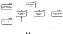
- FIG. 1 depicts a block diagram for a transmitter device with pulse shaping capabilities, consistent with embodiments of the present disclosure.
- the transmitter device shown in FIG. 1 can be used to modulate a received RF carrier signal according to a communication protocol. More particularly, an RF carrier signal can be received from a transmitter circuit and associated coil 112.
- the RF carrier signal can be processed by an RF carrier circuit 104 to produce an output signal that can be used by modulation circuit 106 to provide load modulation, which can be ALM in various embodiments.
- the RF carrier circuit 104 can include a phase-locked loop (PLL) circuit that is driven by the received RF carrier signal.
- PLL phase-locked loop
- Base band data source and encoder circuit 102 can be configured to retrieve data from a memory circuit or other source.
- the data can then be encoded according to a particular transport protocol and using, for example Miller coding or Manchester coding.
- the transport protocol defines data communications according to data frames that have start and stops defined with particular coding patterns.
- the transport protocol can indicate the end of a frame (EOF) (also referred to as end-of-communication or "EOC”), at least in part, by the presence of at least one unmodulated symbol period.
- EEF end-of-communication
- Modulation circuit 106 can be configured to provide an ALM control signal that is based upon the output from the RF carrier circuit 104 and the baseband data source and encoder circuit 102.
- the ALM control signal can produce an RF signal that is phase-aligned with the received RF carrier signal and that is windowed or gated by the output of the baseband data source and encoder circuit 102.
- the output of modulation circuit 106 is a set of pulses for corresponding symbol periods. Each pulse can be generated from windowing the RF signal according to the encoding protocol and at a subcarrier frequency.
- NFC communications can use a 13.56 MHz RF carrier signal, while the subcarrier frequency can be around 848 KHz.
- the subcarrier can then be modulated by the encoded data signal at a bit rate of 106 kBit/s. Accordingly, each bit can contain multiple subcarrier pulses and each subcarrier pulse can contain multiple RF signal pulses.
- Pattern detection circuit 108 can be configured to detect a particular encoding/symbol pattern for the data encoded by baseband data source and encoder circuit 102.
- the pattern detection circuit 108 can be configured to detect an unmodulated symbol period (e.g., indicating an EOF) that is preceded by a particular symbol having a transient that can carry over into the unmodulated symbol period. This particular symbol may include modulation of the RF carrier signal in the second half of a time period for the particular symbol.
- the pattern detection circuit 108 can provide a notification signal to a pulse shaping circuit 110.
- the output of pulse shaping circuit 110 can be provided to a transmitter circuit and a coil 112 for transmission of the data from baseband data source and encoder circuit 102 (via load modulation of the RF carrier signal).
- the pulse shaping circuit 110 can be configured to respond to a notification from the pattern detection circuit 108 by adjusting a pulse in the symbol preceding the unmodulated symbol period.
- the adjustment can include shortening the subcarrier pulse duration by adjusting the windowing of the RF carrier signal for a last subcarrier pulse in the symbol preceding the unmodulated symbol period (or just the "preceding symbol").
- the adjustment can include completely removing the last subcarrier pulse from the preceding symbol.
- Pulse shaping circuit 110 can also be configured to shift the timing of the last subcarrier pulse earlier in the preceding symbol period. In certain embodiments, pulse shaping circuit 110 can be configured to lessen the amplitude of the signal.
- Pulse shaping circuit 110 can be configured to use one or more combinations of the different pulse shaping adjustments discussed herein.
- the last subcarrier pulse could be shifted in time and shortened in duration.
- the drive strength of the ALM could be lessened along with a shifting of the subcarrier pulse timing, a shortening of the subcarrier pulse duration, or both shifting and shortening.
- amplitude reduction can be used with one or both of shifting and shortening of the subcarrier pulses. Pulse shaping adjustments other than those expressly stated herein can also be used.
- pulse shaping circuit 110 can provide pulse shaping for subcarrier pulses that are not identified by pattern detection circuit 108. This pulse shaping can be used for overshoot and undershoot protection. This can include producing wave shapes that comply with specification requirements (consider an example of how the prior pattern was modified). When a signal from pattern detection circuit 108 is received, however, pulse shaping circuit 110 can provide a different adjustment relative to the other subcarrier pulses.
- the circuits depicted in FIG. 1 can be implemented using a specially-programmed processor circuit or microcontroller circuit, programmable logic device (PLD), discrete logic, or combinations thereof.
- PLD programmable logic device
- multiple ones of the depicted circuits can use the same circuitry (e.g., using a common microcontroller).
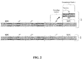
- FIG. 2 depicts a timing diagram for communication frames, consistent with embodiments of the present disclosure.
- FIG. 2 shows timing diagrams for two different frames 202, 204.
- Each of the frames begins with a start-of-communication (SOC) pattern and ends with an end-of-communication (EOC) pattern.
- SOC start-of-communication
- EOC end-of-communication
- each symbol period is divided into two portions, corresponding to a first half and a second half of the symbol period. Modulation of the RF carrier signal in the first half of the symbol can represent a binary "1," while modulation of the RF carrier signal in the second half of the symbol can represent a binary "0.” It is understood that the binary values and associated symbol portions are arbitrary, and further, that different encoding schemes can be used.
- the transmission of frame 202 is depicted with the last data bit corresponding to a "0" value, which results in modulation occurring at, or near, the end of the symbol period.
- the symbol period that immediately follows represents an EOC for which there is no modulation during the symbol period. This can result in a transient from the modulation appearing in the first half of the symbol period for the EOC, which would then be interpreted as a "1" value instead of an EOC.
- a pattern detection circuit can be configured to detect this pattern, where there is a "0" bit followed by an EOC. More generally, the pattern can be modulated in the second half of a symbol period that is followed by an unmodulated symbol period (which can correspond to an EOC).
- a subcarrier pulse of the symbol preceding the EOC can be shaped in the manner discussed herein so as to remove or mitigate the transient relative to the EOC.
- the transmission of frame 204 is depicted with the last data bit corresponding to a "1" value, which results in the modulation occurring at, or near, the beginning of the symbol period (in this case throughout the first half of the symbol period.
- the transient from the modulation is not present in the EOC in any meaningful amount, if at all. Accordingly, the pattern detection circuit will not detect this pattern as requiring pulse shaping relative to a transient in the EOC.
- FIG. 2 shows a signaling scheme that is based upon a symbol period that is split into two halves with modulation occurring during either of the halves
- the pattern detection circuit can be configured to accommodate such schemes by detecting patterns in which modulation occurs in the second half of the symbol period (whether or not the modulation occurs during the entire second half of the symbol period).
- the pattern detection circuit can be configured to detect more specific patterns, such as discriminating between patterns based upon whether or not modulation occurs at the end (or sufficiently close to the end) of the symbol period to result in unwanted transients in the following symbol.
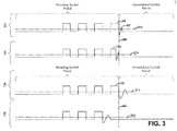
- FIG. 3 depicts a timing diagram for subcarrier pulses, consistent with embodiments of the present disclosure.
- a first timing diagram 302 shows a communication pattern where the subcarrier pulses occur near the end of the last data-carrying symbol period, which is the symbol period immediately preceding the unmodulated symbol period (e.g., representing the EOC).
- each of the subcarrier pulses can be generated using ALM.
- the last pulse 310 ends proximate to the unmodulated symbol period resulting in a situation where the transient 312 is sufficient to cause a false reading in the unmodulated period. For example, if the detection threshold 314 for modulation is exceeded, then the receiver circuit may decode the unmodulated symbol period as carrying valid data (e.g., a "1" if using the encoding described in connection with FIG. 2 ).
- Timing diagram 304 shows the same communication pattern as diagram 302 with additional pulse shaping.
- the pulse shaping involves shortening the duration of the pulse 310 such that some, or all, of the transient is moved from the unmodulated symbol period to the preceding symbol period.
- reducing the duration of the pulse can also reduce the strength of the transient, which can further reduce the likelihood of a false data bit being detected.
- Timing diagram 306 shows a communication pattern where the subcarrier pulses occur near the end of the last data-carrying symbol period, which is the symbol period immediately preceding the unmodulated symbol period (e.g., representing the EOC). Relative to timing diagrams 302 and 304, the duration that the transient is above the threshold 314 is longer and simply shortening the duration of the last pulse 310 may be insufficient. Accordingly, the pulse shaping shown by timing diagram 308 includes completely removing the last pulse 310.
- each of the pulse shaping solutions depicted in timing diagrams 304 and 308 can be done in combination with a reduction in the amplitude of the pulses.
- the reduction can be accomplished by reducing the drive strength of the ALM (or by using only passive load modulation).
- the last pulse 310 can be completely removed while the second to last pulse can also be shortened.
- FIG. 4 depicts a flow diagram for use with a transmitter device with pulse shaping capabilities, consistent with embodiments of the present disclosure.
- the flow beings at block 402 with start of a transmission.
- the transmitter device determines whether or not transient compensation, consistent with the discussion herein, is enabled at decision block 404. If transient compensation is not enabled, then a standard pulse shaping profile (or no pulse shaping at all) can be used, per block 406. If transient compensation is enabled, the transmitter device can attempt to detect a particular pattern that is subject to problems with transients, per block 410.
- the transmitter device may always have transient compensation enabled, in which case, decision block 404 can be skipped.
- Various embodiments allow for transient compensation to be selectively enabled.
- the transient compensation could be determined based upon a manufacturer setting that corresponds to the particular type of device and/or application for which the transmitter is being used (e.g., a cellular telephone vs a laptop computer). This allows the transmitter circuit to be configured for different applications, some of which may not need or benefit from transient compensation.
- the enable condition can be dynamically set based upon failed communication attempts. For example, the transient compensation could start out disabled and be enabled in response to a failed attempt at communication (e.g., due to a false bit caused by a transient in an unmodulated symbol period).
- the transmitter device does not detect a particular pattern (e.g., a particular bit in a symbol period that proceeds an unmodulated symbol period), then the standard pulse shaping profile (or no pulse shaping at all) can be used, per block 406. If the particular pattern is detected by the transmitter device, then a transient profile can be applied for pulse shaping, per block 412.
- a particular pattern e.g., a particular bit in a symbol period that proceeds an unmodulated symbol period
- the transmitter device can optionally change and adjust the dynamically transient profile in response to feedback from the system, per blocks 414 and 416. This can include, for example, providing feedback about unsuccessful communication attempts. In response, the transmitter device could change the transient profile to more aggressively shape the pulse by, for example, reducing the pulse duration further. If this optional adjustment to the transient profile is not used, then the flow can return to block 404 directly from block 412.
- a "block” also sometimes “circuit”, “logic circuitry”, or “module”
- a hard-wired control block can be used to minimize the area for such an implementation in case a limited flexibility is sufficient.
- one or more modules are discreet logic circuits or programmable logic circuits configured and arranged for implementing these operations/activities.
Landscapes
- Engineering & Computer Science (AREA)
- Computer Networks & Wireless Communication (AREA)
- Signal Processing (AREA)
- Physics & Mathematics (AREA)
- Power Engineering (AREA)
- Toxicology (AREA)
- Health & Medical Sciences (AREA)
- General Physics & Mathematics (AREA)
- Theoretical Computer Science (AREA)
- Spectroscopy & Molecular Physics (AREA)
- Microelectronics & Electronic Packaging (AREA)
- Computer Hardware Design (AREA)
- Electromagnetism (AREA)
- General Health & Medical Sciences (AREA)
- Artificial Intelligence (AREA)
- Computer Vision & Pattern Recognition (AREA)
- Near-Field Transmission Systems (AREA)
Abstract
Description
- Aspects of various embodiments are directed to pulse shaping or wave shaping by a transmitter, more particular aspects are directed toward pulse shaping for a transmitter that uses load modulation, such as active load modulation (ALM).
- Certain wireless radio frequency (RF) communication protocols are designed to facilitate transmitter circuits that occupy a small physical footprint, are relatively inexpensive, and consume low amounts of power. One such communication protocol is referred to as near-field communication (NFC) protocol. NFC devices can use magnetic induction (near field communications) between two antennas to effect communications. The NFC protocol specifies the use of an unlicensed radio frequency ISM band of 13.56 MHz.
- NFC-enabled devices can support three modes of operation: card-emulation mode, peer-to-peer mode, and reader/writer mode. NFC technology for the different operating modes are based on the ISO/IEC 18092 NFC IP-1, JIS X 6319-4 and ISO/IEC 14443 contactless smart card standards (sometimes referred to as NFC-A, NFC-B and NFC-F).. In card emulation mode, an NFC-capable device functions like a smart card to allow for existing infrastructure, normally used with smart cards, to be used to perform transactions such as credit/debit purchases and ticketing.
- NFC-capable devices that operate in card emulation mode can use load modulation of a received RF signal to transmit data. The NFC-capable devices may suffer from problems associated with poor modulation amplitude, such as small functional communication distances that are worsened by antenna orientation mismatches. Active load modulation can increase the modulation amplitude but may have undesired side-effects.
- These and other matters have presented challenges to efficiencies of wireless communication devices, methods, and implementations, for a variety of applications.
- According to a first aspect of the present disclosure, a method for compensating for transients caused by load modulation by adjusting pulse shapes is conceived, the method comprising: modulating a radio frequency (RF) carrier signal using load modulation; detecting, for the modulated RF carrier signal, a particular symbol pattern for a first symbol that precedes a second symbol that does not use load modulation; and adjusting, in response to the detecting, a pulse shape of the first symbol to mitigate the transients.
- In one or more embodiments of the method, the detecting further includes detecting that the first symbol uses active load modulation in a second half of the first symbol.
- In one or more embodiments of the method, the first symbol includes a series of pulses located at a second half of the first symbol.
- In one or more embodiments of the method, the adjusting further includes shortening a duration for a pulse of the series of pulses.
- In one or more embodiments of the method, the adjusting further includes removing a pulse form the series of pulses.
- In one or more embodiments of the method, the adjusting further includes removing multiple pulses form the series of pulses.
- In one or more embodiments of the method, the adjusting further includes reducing an amplitude for the series of pulses.
- In one or more embodiments of the method, the adjusting further includes shortening a duration for a pulse of the series of pulses, removing at least one pulse form the series of pulses, and reducing an amplitude for the series of pulses.
- In one or more embodiments of the method, the adjusting is responsive to feedback that is based upon a transient of the first symbol being detected in the second symbol.
- In one or more embodiments of the method, the modulation of the RF carrier signal is consistent with NFC protocols for a card-emulation mode.
- According to a second aspect of the present disclosure, a device is provided, comprising a modulation circuit configured to modulate a radio frequency (RF) carrier signal using load modulation and according to a plurality of symbols; a detection circuit configured to detect, for the modulated RF carrier signal, a first symbol pattern of a first symbol preceding a second symbol pattern of a second symbol that does not use load modulation; and a pulse shaping circuit configured to adjust, in response to the detection circuit, a pulse shape of the first symbol to mitigate transients in the second symbol.
- In one or more embodiments of the device, the detection circuit is further configured to detect that the first symbol uses active load modulation in a second half of the first symbol.
- In one or more embodiments of the device, the first symbol includes a series of pulses located at a second half of the first symbol.
- In one or more embodiments of the device, the pulse shaping circuit is further configured to adjust the pulse shape of the first symbol by shortening a duration for a pulse of the series of pulses.
- In one or more embodiments of the device, the pulse shaping circuit is further configured to adjust the pulse shape of the first symbol by removing a pulse form the series of pulses.
- In one or more embodiments of the device, the pulse shaping circuit is further configured to adjust the pulse shape of the first symbol by removing multiple pulses form the series of pulses.
- In one or more embodiments of the device, the pulse shaping circuit is further configured to adjust the pulse shape of the first symbol by reducing an amplitude for the series of pulses.
- In one or more embodiments of the device, the pulse shaping circuit is further configured to adjust the pulse shape of the first symbol in response to feedback that is based upon transients of the first symbol being detected in the second symbol.
- In one or more embodiments of the device, the RF carrier signal and the plurality of symbols are consistent with NFC protocols for a card-emulation mode.
- The above discussion/summary is not intended to describe each embodiment or every implementation of the present disclosure. The figures and detailed description that follow also exemplify various embodiments.
- Various example embodiments may be more completely understood in consideration of the following detailed description in connection with the accompanying drawings, in which:
-
FIG. 1 depicts a block diagram for a transmitter device with pulse shaping capabilities, consistent with embodiments of the present disclosure; -
FIG. 2 depicts a timing diagram for communication frames, consistent with embodiments of the present disclosure; -
FIG. 3 depicts a timing diagram for subcarrier pulses, consistent with embodiments of the present disclosure; and -
FIG. 4 depicts a flow diagram for use with a transmitter device with pulse shaping capabilities, consistent with embodiments of the present disclosure. - While various embodiments discussed herein are amenable to modifications and alternative forms, aspects thereof have been shown by way of example in the drawings and will be described in detail. It should be understood, however, that the intention is not to limit the invention to the particular embodiments described. On the contrary, the intention is to cover all modifications, equivalents, and alternatives falling within the scope of the disclosure including aspects defined in the claims. In addition, the term "example" as used throughout this application is only by way of illustration, and not limitation.
- Aspects of the present disclosure are believed to be applicable to a variety of different types of apparatuses, systems and methods involving pulse shaping in response to detected symbol patterns and combinations. In certain implementations, aspects of the present disclosure have been shown to be beneficial when used in the context of NFC-capable devices. In some embodiments, the NFC-capable devices use ALM in a card emulation mode. These and other aspects can be implemented to address challenges, including those discussed in the background above. While not necessarily so limited, various aspects may be appreciated through a discussion of examples using such exemplary contexts.
- Various embodiments of the present disclosure are directed toward the mitigation of transient responses in wireless communications. For instance, a transmitter device can include circuits that are configured to detect specific communication pattern(s) that are subject to communication errors caused by transient responses and to modify a pulse shape for the detected communication patterns. Particular embodiments are directed toward transients resulting from the use of load modulation (such as ALM) in a communication protocol that also uses the lack of modulation to convey data, such as identifying the end of a communication with an unmodulated symbol period. The circuits can be configured to detect an end of communication condition and to adjust, in response to the detection, the pulse shape of a preceding symbol in a manner that mitigates a transient from the adjusted pulse.
- In some instances, the circuits can be configured to detect a communication pattern where a symbol corresponding to a particular type(s) of symbol immediately precedes an unmodulated symbol period. In response to this detection, the pulse shape of the preceding symbol can be adjusted to mitigate a transient in the unmodulated symbol period.
- Consistent with embodiments, the adjustment of the pulse shape can include shortening the duration of the pulse. For instance, the end of the pulse can be moved earlier in time so that there is more time between the end of the pulse and the unmodulated symbol period. This can be particularly useful for shifting the timing of the corresponding transient earlier so that some, or all, of the transient is no longer present during the unmodulated symbol period.
- In particular embodiments, the circuits can be configured to communicate using NFC protocols, and more particularly, using ALM as part of a card emulation mode. As discussed in more detail herein, the card emulation mode can include a communication pattern where at least a portion of the second half of a symbol is modulated and that symbol is immediately followed by an unmodulated symbol that identifies the end of the communication. Accordingly, a transient from the second half of the symbol that appears in the unmodulated symbol can result in a receiver circuit incorrectly detecting modulation during the unmodulated symbol.
- While various embodiments are discussed in the context of ALM, it is recognized that transmitters that use passive load modulation can also suffer from problems with transients in unmodulated symbols. Accordingly, the various types of pulse shaping discussed herein can be generally also be applied in connection with passive load modulation.
- Turning now to the figures,
FIG. 1 depicts a block diagram for a transmitter device with pulse shaping capabilities, consistent with embodiments of the present disclosure. The transmitter device shown inFIG. 1 can be used to modulate a received RF carrier signal according to a communication protocol. More particularly, an RF carrier signal can be received from a transmitter circuit and associatedcoil 112. The RF carrier signal can be processed by anRF carrier circuit 104 to produce an output signal that can be used bymodulation circuit 106 to provide load modulation, which can be ALM in various embodiments. For instance, theRF carrier circuit 104 can include a phase-locked loop (PLL) circuit that is driven by the received RF carrier signal. - Base band data source and
encoder circuit 102 can be configured to retrieve data from a memory circuit or other source. The data can then be encoded according to a particular transport protocol and using, for example Miller coding or Manchester coding. In certain embodiments, the transport protocol defines data communications according to data frames that have start and stops defined with particular coding patterns. For example, the transport protocol can indicate the end of a frame (EOF) (also referred to as end-of-communication or "EOC"), at least in part, by the presence of at least one unmodulated symbol period. -
Modulation circuit 106 can be configured to provide an ALM control signal that is based upon the output from theRF carrier circuit 104 and the baseband data source andencoder circuit 102. In particular, the ALM control signal can produce an RF signal that is phase-aligned with the received RF carrier signal and that is windowed or gated by the output of the baseband data source andencoder circuit 102. Consistent with embodiments, the output ofmodulation circuit 106 is a set of pulses for corresponding symbol periods. Each pulse can be generated from windowing the RF signal according to the encoding protocol and at a subcarrier frequency. For example, NFC communications can use a 13.56 MHz RF carrier signal, while the subcarrier frequency can be around 848 KHz. The subcarrier can then be modulated by the encoded data signal at a bit rate of 106 kBit/s. Accordingly, each bit can contain multiple subcarrier pulses and each subcarrier pulse can contain multiple RF signal pulses. - The output of the
ALM circuit 106 can then be provided topulse shaping circuit 110, which is configured to adjust the subcarrier pulse shape in response to a signal provided bypattern detection circuit 108.Pattern detection circuit 108 can be configured to detect a particular encoding/symbol pattern for the data encoded by baseband data source andencoder circuit 102. For example, thepattern detection circuit 108 can be configured to detect an unmodulated symbol period (e.g., indicating an EOF) that is preceded by a particular symbol having a transient that can carry over into the unmodulated symbol period. This particular symbol may include modulation of the RF carrier signal in the second half of a time period for the particular symbol. Upon detection of the particular pattern, thepattern detection circuit 108 can provide a notification signal to apulse shaping circuit 110. The output ofpulse shaping circuit 110 can be provided to a transmitter circuit and acoil 112 for transmission of the data from baseband data source and encoder circuit 102 (via load modulation of the RF carrier signal). - According to embodiments of the present disclosure, the
pulse shaping circuit 110 can be configured to respond to a notification from thepattern detection circuit 108 by adjusting a pulse in the symbol preceding the unmodulated symbol period. In some embodiments, the adjustment can include shortening the subcarrier pulse duration by adjusting the windowing of the RF carrier signal for a last subcarrier pulse in the symbol preceding the unmodulated symbol period (or just the "preceding symbol"). In various embodiments, the adjustment can include completely removing the last subcarrier pulse from the preceding symbol.Pulse shaping circuit 110 can also be configured to shift the timing of the last subcarrier pulse earlier in the preceding symbol period. In certain embodiments,pulse shaping circuit 110 can be configured to lessen the amplitude of the signal. This can be done by lessening the drive strength for the ALM of the last subcarrier pulse, or use (passive) load modulation for the last subcarrier pulse.Pulse shaping circuit 110 can be configured to use one or more combinations of the different pulse shaping adjustments discussed herein. For example, the last subcarrier pulse could be shifted in time and shortened in duration. As another example, the drive strength of the ALM could be lessened along with a shifting of the subcarrier pulse timing, a shortening of the subcarrier pulse duration, or both shifting and shortening. Further, amplitude reduction can be used with one or both of shifting and shortening of the subcarrier pulses. Pulse shaping adjustments other than those expressly stated herein can also be used. - In certain embodiments,
pulse shaping circuit 110 can provide pulse shaping for subcarrier pulses that are not identified bypattern detection circuit 108. This pulse shaping can be used for overshoot and undershoot protection. This can include producing wave shapes that comply with specification requirements (consider an example of how the prior pattern was modified). When a signal frompattern detection circuit 108 is received, however,pulse shaping circuit 110 can provide a different adjustment relative to the other subcarrier pulses. - Consistent with embodiments, the circuits depicted in
FIG. 1 can be implemented using a specially-programmed processor circuit or microcontroller circuit, programmable logic device (PLD), discrete logic, or combinations thereof. In some embodiments, multiple ones of the depicted circuits can use the same circuitry (e.g., using a common microcontroller). -
FIG. 2 depicts a timing diagram for communication frames, consistent with embodiments of the present disclosure.FIG. 2 shows timing diagrams for twodifferent frames FIG. 2 , each symbol period is divided into two portions, corresponding to a first half and a second half of the symbol period. Modulation of the RF carrier signal in the first half of the symbol can represent a binary "1," while modulation of the RF carrier signal in the second half of the symbol can represent a binary "0." It is understood that the binary values and associated symbol portions are arbitrary, and further, that different encoding schemes can be used. - The transmission of
frame 202 is depicted with the last data bit corresponding to a "0" value, which results in modulation occurring at, or near, the end of the symbol period. The symbol period that immediately follows represents an EOC for which there is no modulation during the symbol period. This can result in a transient from the modulation appearing in the first half of the symbol period for the EOC, which would then be interpreted as a "1" value instead of an EOC. As discussed herein, a pattern detection circuit can be configured to detect this pattern, where there is a "0" bit followed by an EOC. More generally, the pattern can be modulated in the second half of a symbol period that is followed by an unmodulated symbol period (which can correspond to an EOC). In response, a subcarrier pulse of the symbol preceding the EOC can be shaped in the manner discussed herein so as to remove or mitigate the transient relative to the EOC. - The transmission of
frame 204 is depicted with the last data bit corresponding to a "1" value, which results in the modulation occurring at, or near, the beginning of the symbol period (in this case throughout the first half of the symbol period. As such, the transient from the modulation is not present in the EOC in any meaningful amount, if at all. Accordingly, the pattern detection circuit will not detect this pattern as requiring pulse shaping relative to a transient in the EOC. - While
FIG. 2 shows a signaling scheme that is based upon a symbol period that is split into two halves with modulation occurring during either of the halves, other signaling schemes are possible. The pattern detection circuit can be configured to accommodate such schemes by detecting patterns in which modulation occurs in the second half of the symbol period (whether or not the modulation occurs during the entire second half of the symbol period). In certain embodiments, the pattern detection circuit can be configured to detect more specific patterns, such as discriminating between patterns based upon whether or not modulation occurs at the end (or sufficiently close to the end) of the symbol period to result in unwanted transients in the following symbol. -
FIG. 3 depicts a timing diagram for subcarrier pulses, consistent with embodiments of the present disclosure. A first timing diagram 302 shows a communication pattern where the subcarrier pulses occur near the end of the last data-carrying symbol period, which is the symbol period immediately preceding the unmodulated symbol period (e.g., representing the EOC). As discussed herein, each of the subcarrier pulses can be generated using ALM. Thelast pulse 310 ends proximate to the unmodulated symbol period resulting in a situation where the transient 312 is sufficient to cause a false reading in the unmodulated period. For example, if thedetection threshold 314 for modulation is exceeded, then the receiver circuit may decode the unmodulated symbol period as carrying valid data (e.g., a "1" if using the encoding described in connection withFIG. 2 ). - Timing diagram 304 shows the same communication pattern as diagram 302 with additional pulse shaping. In particular, the pulse shaping involves shortening the duration of the
pulse 310 such that some, or all, of the transient is moved from the unmodulated symbol period to the preceding symbol period. Moreover, reducing the duration of the pulse can also reduce the strength of the transient, which can further reduce the likelihood of a false data bit being detected. - Timing diagram 306 shows a communication pattern where the subcarrier pulses occur near the end of the last data-carrying symbol period, which is the symbol period immediately preceding the unmodulated symbol period (e.g., representing the EOC). Relative to timing diagrams 302 and 304, the duration that the transient is above the
threshold 314 is longer and simply shortening the duration of thelast pulse 310 may be insufficient. Accordingly, the pulse shaping shown by timing diagram 308 includes completely removing thelast pulse 310. - As discussed herein, the pulse shaping can be done in other manners and combinations. For instance, each of the pulse shaping solutions depicted in timing diagrams 304 and 308 can be done in combination with a reduction in the amplitude of the pulses. The reduction can be accomplished by reducing the drive strength of the ALM (or by using only passive load modulation). In some instances, the
last pulse 310 can be completely removed while the second to last pulse can also be shortened. -
FIG. 4 depicts a flow diagram for use with a transmitter device with pulse shaping capabilities, consistent with embodiments of the present disclosure. The flow beings atblock 402 with start of a transmission. The transmitter device determines whether or not transient compensation, consistent with the discussion herein, is enabled atdecision block 404. If transient compensation is not enabled, then a standard pulse shaping profile (or no pulse shaping at all) can be used, perblock 406. If transient compensation is enabled, the transmitter device can attempt to detect a particular pattern that is subject to problems with transients, perblock 410. - In some embodiments, the transmitter device may always have transient compensation enabled, in which case,
decision block 404 can be skipped. Various embodiments allow for transient compensation to be selectively enabled. For example, the transient compensation could be determined based upon a manufacturer setting that corresponds to the particular type of device and/or application for which the transmitter is being used (e.g., a cellular telephone vs a laptop computer). This allows the transmitter circuit to be configured for different applications, some of which may not need or benefit from transient compensation. In some instances, the enable condition can be dynamically set based upon failed communication attempts. For example, the transient compensation could start out disabled and be enabled in response to a failed attempt at communication (e.g., due to a false bit caused by a transient in an unmodulated symbol period). - If the transmitter device does not detect a particular pattern (e.g., a particular bit in a symbol period that proceeds an unmodulated symbol period), then the standard pulse shaping profile (or no pulse shaping at all) can be used, per
block 406. If the particular pattern is detected by the transmitter device, then a transient profile can be applied for pulse shaping, perblock 412. - Consistent with some embodiments, the transmitter device can optionally change and adjust the dynamically transient profile in response to feedback from the system, per
blocks block 412. - Various blocks, modules or other circuits may be implemented to carry out one or more of the operations and activities described herein and/or shown in the figures. In these contexts, a "block" (also sometimes "circuit", "logic circuitry", or "module") can be implemented using a circuit that carries out one or more of these or related operations/activities. In various embodiments, a hard-wired control block can be used to minimize the area for such an implementation in case a limited flexibility is sufficient. Alternatively and/or in addition, in certain of the above-discussed embodiments, one or more modules are discreet logic circuits or programmable logic circuits configured and arranged for implementing these operations/activities.
- Based upon the above discussion and illustrations, those skilled in the art will readily recognize that various modifications and changes may be made to the various embodiments without strictly following the exemplary embodiments and applications illustrated and described herein. For example, an apparatus can include different signal processing components and use different encoding and modulation techniques and configurations than illustrated by the various Figures. Further, the various embodiments and associated features can be used in a variety of different combinations, some of which are not expressly stated for brevity. Such modifications do not depart from the true spirit and scope of various aspects of the invention, including aspects set forth in the claims.
Claims (15)
- A method for compensating for transients caused by load modulation by adjusting pulse shapes, the method comprising:modulating a radio frequency (RF) carrier signal using load modulation;detecting, for the modulated RF carrier signal, a particular symbol pattern for a first symbol that precedes a second symbol that does not use load modulation; andadjusting, in response to the detecting, a pulse shape of the first symbol to mitigate the transients.
- The method of claim 1, wherein the detecting further includes detecting that the first symbol uses active load modulation in a second half of the first symbol.
- The method of claim 1 or 2, wherein the first symbol includes a series of pulses located at a second half of the first symbol.
- The method of claim 3, wherein the adjusting further includes shortening a duration for a pulse of the series of pulses.
- The method of claim 3 or 4, wherein the adjusting further includes removing a pulse from the series of pulses.
- The method of any one of claims 3 to 5, wherein the adjusting further includes removing multiple pulses from the series of pulses.
- The method of any one of claims 3 to 6, wherein the adjusting further includes reducing an amplitude for the series of pulses.
- The method of any one of claims 3 to 7, wherein the adjusting further includes shortening a duration for a pulse of the series of pulses, removing at least one pulse from the series of pulses, and reducing an amplitude for the series of pulses.
- The method of any preceding claim, wherein the adjusting is responsive to feedback that is based upon a transient of the first symbol being detected in the second symbol.
- The method of any preceding claim, wherein the modulation of the RF carrier signal is consistent with NFC protocols for a card-emulation mode.
- A device comprising
a modulation circuit configured to modulate a radio frequency (RF) carrier signal using load modulation and according to a plurality of symbols;
a detection circuit configured to detect, for the modulated RF carrier signal, a first symbol pattern of a first symbol preceding a second symbol pattern of a second symbol that does not use load modulation; and
a pulse shaping circuit configured to adjust, in response to the detection circuit, a pulse shape of the first symbol to mitigate transients in the second symbol. - The device of claim 11, wherein the detection circuit is further configured to detect that the first symbol uses active load modulation in a second half of the first symbol.
- The device of claim 11 or 12, wherein the first symbol includes a series of pulses located at a second half of the first symbol.
- The device of claim 13, wherein the pulse shaping circuit is further configured to adjust the pulse shape of the first symbol by shortening a duration for a pulse of the series of pulses.
- The device of claim 13 or 14, wherein the pulse shaping circuit is further configured to adjust the pulse shape of the first symbol by removing a pulse from the series of pulses.
Applications Claiming Priority (1)
| Application Number | Priority Date | Filing Date | Title |
|---|---|---|---|
| US14/847,810 US9742443B2 (en) | 2015-09-08 | 2015-09-08 | Pulse shaping for radio frequency transmitters |
Publications (2)
| Publication Number | Publication Date |
|---|---|
| EP3142311A1 true EP3142311A1 (en) | 2017-03-15 |
| EP3142311B1 EP3142311B1 (en) | 2019-11-13 |
Family
ID=56925967
Family Applications (1)
| Application Number | Title | Priority Date | Filing Date |
|---|---|---|---|
| EP16185151.4A Active EP3142311B1 (en) | 2015-09-08 | 2016-08-22 | Pulse shaping for radio frequency transmitters |
Country Status (3)
| Country | Link |
|---|---|
| US (1) | US9742443B2 (en) |
| EP (1) | EP3142311B1 (en) |
| CN (1) | CN106506416B (en) |
Families Citing this family (3)
| Publication number | Priority date | Publication date | Assignee | Title |
|---|---|---|---|---|
| US10396975B2 (en) | 2016-06-29 | 2019-08-27 | Maxim Integrated Products, Inc. | Clock recovery system and method for near field communication with active load modulation |
| US12047284B2 (en) * | 2018-08-27 | 2024-07-23 | Drivenets Ltd. | System and a method for using a network cloud software |
| FR3102625B1 (en) * | 2019-10-28 | 2021-11-12 | St Microelectronics Sa | NFC device emulated in card mode comprising a digital phase-locked loop, and corresponding communication method. |
Citations (3)
| Publication number | Priority date | Publication date | Assignee | Title |
|---|---|---|---|---|
| WO2009148372A1 (en) * | 2008-06-05 | 2009-12-10 | Telefonaktiebolaget L M Ericsson (Publ) | Method and arrangement in a cellular communications system |
| US20140004794A1 (en) * | 2012-07-02 | 2014-01-02 | Marvell World Trade Ltd. | Shaping Near-Field Transmission Signals |
| WO2015036682A1 (en) * | 2013-09-13 | 2015-03-19 | Inside Secure | Method and device for transmitting data by inductive coupling with controlled self-oscillation |
Family Cites Families (10)
| Publication number | Priority date | Publication date | Assignee | Title |
|---|---|---|---|---|
| US6144862A (en) * | 1998-07-28 | 2000-11-07 | Motorola, Inc. | Pulse-shaping look-up table with transient suppression |
| US7002483B2 (en) * | 2001-07-11 | 2006-02-21 | Trw Inc. | Configurable arrangement of multiple transmitters and multiple receivers for the performance of remote convenience functions |
| KR100450765B1 (en) * | 2002-10-11 | 2004-10-02 | 한국전자통신연구원 | Wireless communication medium and method for operation thereof |
| DE102004020816A1 (en) * | 2004-04-22 | 2005-11-17 | Atmel Germany Gmbh | Method and circuit for load modulation in a connection of a transmitting oscillating circuit and a receiving resonant circuit |
| US7868600B2 (en) * | 2005-11-16 | 2011-01-11 | Intersil Americas Inc. | Adaptive PWM pulse positioning for fast transient response |
| JP4525747B2 (en) * | 2007-02-20 | 2010-08-18 | セイコーエプソン株式会社 | Power transmission control device, power transmission device, electronic device, and non-contact power transmission system |
| CN102196605B (en) * | 2010-03-15 | 2014-02-26 | 国民技术股份有限公司 | Mobile radio frequency device, radio frequency IC (Integrated Circuit) card and radio frequency storage card |
| WO2013176751A1 (en) * | 2012-05-20 | 2013-11-28 | Access Business Group International Llc | System and method for communication in wireless power supply systems |
| US8902965B2 (en) * | 2012-09-27 | 2014-12-02 | Qualcomm Incorporated | Pulse shaping for generating NFC initiator transmit waveform |
| US9042816B2 (en) * | 2012-11-05 | 2015-05-26 | Qualcomm Incorporated | Methods and apparatus for improving NFC coil tuning based on proximity to a remote NFC device |
-
2015
- 2015-09-08 US US14/847,810 patent/US9742443B2/en active Active
-
2016
- 2016-08-22 EP EP16185151.4A patent/EP3142311B1/en active Active
- 2016-09-06 CN CN201610806615.2A patent/CN106506416B/en active Active
Patent Citations (4)
| Publication number | Priority date | Publication date | Assignee | Title |
|---|---|---|---|---|
| WO2009148372A1 (en) * | 2008-06-05 | 2009-12-10 | Telefonaktiebolaget L M Ericsson (Publ) | Method and arrangement in a cellular communications system |
| US20140004794A1 (en) * | 2012-07-02 | 2014-01-02 | Marvell World Trade Ltd. | Shaping Near-Field Transmission Signals |
| WO2015036682A1 (en) * | 2013-09-13 | 2015-03-19 | Inside Secure | Method and device for transmitting data by inductive coupling with controlled self-oscillation |
| US20160197718A1 (en) * | 2013-09-13 | 2016-07-07 | Inside Secure | Method and device for transmitting data by inductive coupling with controlled self-oscillation |
Also Published As
| Publication number | Publication date |
|---|---|
| CN106506416B (en) | 2020-11-20 |
| CN106506416A (en) | 2017-03-15 |
| US9742443B2 (en) | 2017-08-22 |
| EP3142311B1 (en) | 2019-11-13 |
| US20170070245A1 (en) | 2017-03-09 |
Similar Documents
| Publication | Publication Date | Title |
|---|---|---|
| JP5039856B2 (en) | Electronic device and method for communicating via transfer jet and NFC transmitter and receiver pairing | |
| EP2763076B1 (en) | Wireless communications using active modulation | |
| KR101492948B1 (en) | Near field commnunications device having adjustable gain | |
| US8874033B2 (en) | Communication apparatus, communication method, and program | |
| US20130344805A1 (en) | Automatic gain control for an nfc reader demodulator | |
| US20160072556A1 (en) | Feedback-Based Adaptive Load Modulation (ALM) for a Near Field Communication (NFC) Device | |
| EP2779018B1 (en) | Clock synchronization in an RFID equipped device | |
| US9408015B2 (en) | Reducing receiver performance degradation due to frequency coexistence | |
| JP2016517662A (en) | Load modulation of direct power transmission in near field communication devices | |
| KR102883342B1 (en) | Clock recovery circuit for nfc(near field communication) transceiver, nfc transceiver, and operating apparatus, operating method, and training method of network based on domain adaptation | |
| EP3142311B1 (en) | Pulse shaping for radio frequency transmitters | |
| US9520987B2 (en) | Systems and methods for timing recovery in near-field communication | |
| US9654186B2 (en) | Portable terminal | |
| CN116208454B (en) | Device and method for decoding data from a wireless signal | |
| EP1877952B1 (en) | Circuit for a communication device and method of controlling a transmission | |
| US11171687B2 (en) | Method and system for operating a communications device that communicates via inductive coupling | |
| JP2009271775A (en) | Receiving apparatus | |
| EP4012935B1 (en) | Wave-shaping for over- and undershoot prevention | |
| JP2001307031A (en) | Non-contact IC card reader / writer | |
| JP5245860B2 (en) | Non-contact communication device and demodulator | |
| JP4670556B2 (en) | Communication apparatus and method | |
| US20150263789A1 (en) | Circuit arrangement | |
| JP2010109699A (en) | Communication apparatus and semiconductor device |
Legal Events
| Date | Code | Title | Description |
|---|---|---|---|
| PUAI | Public reference made under article 153(3) epc to a published international application that has entered the european phase |
Free format text: ORIGINAL CODE: 0009012 |
|
| STAA | Information on the status of an ep patent application or granted ep patent |
Free format text: STATUS: THE APPLICATION HAS BEEN PUBLISHED |
|
| AK | Designated contracting states |
Kind code of ref document: A1 Designated state(s): AL AT BE BG CH CY CZ DE DK EE ES FI FR GB GR HR HU IE IS IT LI LT LU LV MC MK MT NL NO PL PT RO RS SE SI SK SM TR |
|
| AX | Request for extension of the european patent |
Extension state: BA ME |
|
| STAA | Information on the status of an ep patent application or granted ep patent |
Free format text: STATUS: REQUEST FOR EXAMINATION WAS MADE |
|
| 17P | Request for examination filed |
Effective date: 20170915 |
|
| RBV | Designated contracting states (corrected) |
Designated state(s): AL AT BE BG CH CY CZ DE DK EE ES FI FR GB GR HR HU IE IS IT LI LT LU LV MC MK MT NL NO PL PT RO RS SE SI SK SM TR |
|
| STAA | Information on the status of an ep patent application or granted ep patent |
Free format text: STATUS: EXAMINATION IS IN PROGRESS |
|
| 17Q | First examination report despatched |
Effective date: 20190118 |
|
| GRAP | Despatch of communication of intention to grant a patent |
Free format text: ORIGINAL CODE: EPIDOSNIGR1 |
|
| STAA | Information on the status of an ep patent application or granted ep patent |
Free format text: STATUS: GRANT OF PATENT IS INTENDED |
|
| INTG | Intention to grant announced |
Effective date: 20190621 |
|
| GRAS | Grant fee paid |
Free format text: ORIGINAL CODE: EPIDOSNIGR3 |
|
| GRAA | (expected) grant |
Free format text: ORIGINAL CODE: 0009210 |
|
| STAA | Information on the status of an ep patent application or granted ep patent |
Free format text: STATUS: THE PATENT HAS BEEN GRANTED |
|
| AK | Designated contracting states |
Kind code of ref document: B1 Designated state(s): AL AT BE BG CH CY CZ DE DK EE ES FI FR GB GR HR HU IE IS IT LI LT LU LV MC MK MT NL NO PL PT RO RS SE SI SK SM TR |
|
| REG | Reference to a national code |
Ref country code: CH Ref legal event code: EP Ref country code: AT Ref legal event code: REF Ref document number: 1202850 Country of ref document: AT Kind code of ref document: T Effective date: 20191115 |
|
| REG | Reference to a national code |
Ref country code: DE Ref legal event code: R096 Ref document number: 602016024177 Country of ref document: DE |
|
| REG | Reference to a national code |
Ref country code: IE Ref legal event code: FG4D |
|
| REG | Reference to a national code |
Ref country code: NL Ref legal event code: MP Effective date: 20191113 |
|
| REG | Reference to a national code |
Ref country code: LT Ref legal event code: MG4D |
|
| PG25 | Lapsed in a contracting state [announced via postgrant information from national office to epo] |
Ref country code: LV Free format text: LAPSE BECAUSE OF FAILURE TO SUBMIT A TRANSLATION OF THE DESCRIPTION OR TO PAY THE FEE WITHIN THE PRESCRIBED TIME-LIMIT Effective date: 20191113 Ref country code: SE Free format text: LAPSE BECAUSE OF FAILURE TO SUBMIT A TRANSLATION OF THE DESCRIPTION OR TO PAY THE FEE WITHIN THE PRESCRIBED TIME-LIMIT Effective date: 20191113 Ref country code: NL Free format text: LAPSE BECAUSE OF FAILURE TO SUBMIT A TRANSLATION OF THE DESCRIPTION OR TO PAY THE FEE WITHIN THE PRESCRIBED TIME-LIMIT Effective date: 20191113 Ref country code: PT Free format text: LAPSE BECAUSE OF FAILURE TO SUBMIT A TRANSLATION OF THE DESCRIPTION OR TO PAY THE FEE WITHIN THE PRESCRIBED TIME-LIMIT Effective date: 20200313 Ref country code: GR Free format text: LAPSE BECAUSE OF FAILURE TO SUBMIT A TRANSLATION OF THE DESCRIPTION OR TO PAY THE FEE WITHIN THE PRESCRIBED TIME-LIMIT Effective date: 20200214 Ref country code: PL Free format text: LAPSE BECAUSE OF FAILURE TO SUBMIT A TRANSLATION OF THE DESCRIPTION OR TO PAY THE FEE WITHIN THE PRESCRIBED TIME-LIMIT Effective date: 20191113 Ref country code: NO Free format text: LAPSE BECAUSE OF FAILURE TO SUBMIT A TRANSLATION OF THE DESCRIPTION OR TO PAY THE FEE WITHIN THE PRESCRIBED TIME-LIMIT Effective date: 20200213 Ref country code: FI Free format text: LAPSE BECAUSE OF FAILURE TO SUBMIT A TRANSLATION OF THE DESCRIPTION OR TO PAY THE FEE WITHIN THE PRESCRIBED TIME-LIMIT Effective date: 20191113 Ref country code: LT Free format text: LAPSE BECAUSE OF FAILURE TO SUBMIT A TRANSLATION OF THE DESCRIPTION OR TO PAY THE FEE WITHIN THE PRESCRIBED TIME-LIMIT Effective date: 20191113 Ref country code: BG Free format text: LAPSE BECAUSE OF FAILURE TO SUBMIT A TRANSLATION OF THE DESCRIPTION OR TO PAY THE FEE WITHIN THE PRESCRIBED TIME-LIMIT Effective date: 20200213 |
|
| PG25 | Lapsed in a contracting state [announced via postgrant information from national office to epo] |
Ref country code: HR Free format text: LAPSE BECAUSE OF FAILURE TO SUBMIT A TRANSLATION OF THE DESCRIPTION OR TO PAY THE FEE WITHIN THE PRESCRIBED TIME-LIMIT Effective date: 20191113 Ref country code: RS Free format text: LAPSE BECAUSE OF FAILURE TO SUBMIT A TRANSLATION OF THE DESCRIPTION OR TO PAY THE FEE WITHIN THE PRESCRIBED TIME-LIMIT Effective date: 20191113 Ref country code: IS Free format text: LAPSE BECAUSE OF FAILURE TO SUBMIT A TRANSLATION OF THE DESCRIPTION OR TO PAY THE FEE WITHIN THE PRESCRIBED TIME-LIMIT Effective date: 20200313 |
|
| PG25 | Lapsed in a contracting state [announced via postgrant information from national office to epo] |
Ref country code: AL Free format text: LAPSE BECAUSE OF FAILURE TO SUBMIT A TRANSLATION OF THE DESCRIPTION OR TO PAY THE FEE WITHIN THE PRESCRIBED TIME-LIMIT Effective date: 20191113 |
|
| PG25 | Lapsed in a contracting state [announced via postgrant information from national office to epo] |
Ref country code: RO Free format text: LAPSE BECAUSE OF FAILURE TO SUBMIT A TRANSLATION OF THE DESCRIPTION OR TO PAY THE FEE WITHIN THE PRESCRIBED TIME-LIMIT Effective date: 20191113 Ref country code: EE Free format text: LAPSE BECAUSE OF FAILURE TO SUBMIT A TRANSLATION OF THE DESCRIPTION OR TO PAY THE FEE WITHIN THE PRESCRIBED TIME-LIMIT Effective date: 20191113 Ref country code: DK Free format text: LAPSE BECAUSE OF FAILURE TO SUBMIT A TRANSLATION OF THE DESCRIPTION OR TO PAY THE FEE WITHIN THE PRESCRIBED TIME-LIMIT Effective date: 20191113 Ref country code: ES Free format text: LAPSE BECAUSE OF FAILURE TO SUBMIT A TRANSLATION OF THE DESCRIPTION OR TO PAY THE FEE WITHIN THE PRESCRIBED TIME-LIMIT Effective date: 20191113 Ref country code: CZ Free format text: LAPSE BECAUSE OF FAILURE TO SUBMIT A TRANSLATION OF THE DESCRIPTION OR TO PAY THE FEE WITHIN THE PRESCRIBED TIME-LIMIT Effective date: 20191113 |
|
| REG | Reference to a national code |
Ref country code: DE Ref legal event code: R097 Ref document number: 602016024177 Country of ref document: DE |
|
| REG | Reference to a national code |
Ref country code: AT Ref legal event code: MK05 Ref document number: 1202850 Country of ref document: AT Kind code of ref document: T Effective date: 20191113 |
|
| PG25 | Lapsed in a contracting state [announced via postgrant information from national office to epo] |
Ref country code: SK Free format text: LAPSE BECAUSE OF FAILURE TO SUBMIT A TRANSLATION OF THE DESCRIPTION OR TO PAY THE FEE WITHIN THE PRESCRIBED TIME-LIMIT Effective date: 20191113 Ref country code: SM Free format text: LAPSE BECAUSE OF FAILURE TO SUBMIT A TRANSLATION OF THE DESCRIPTION OR TO PAY THE FEE WITHIN THE PRESCRIBED TIME-LIMIT Effective date: 20191113 |
|
| PLBE | No opposition filed within time limit |
Free format text: ORIGINAL CODE: 0009261 |
|
| STAA | Information on the status of an ep patent application or granted ep patent |
Free format text: STATUS: NO OPPOSITION FILED WITHIN TIME LIMIT |
|
| 26N | No opposition filed |
Effective date: 20200814 |
|
| PG25 | Lapsed in a contracting state [announced via postgrant information from national office to epo] |
Ref country code: SI Free format text: LAPSE BECAUSE OF FAILURE TO SUBMIT A TRANSLATION OF THE DESCRIPTION OR TO PAY THE FEE WITHIN THE PRESCRIBED TIME-LIMIT Effective date: 20191113 Ref country code: AT Free format text: LAPSE BECAUSE OF FAILURE TO SUBMIT A TRANSLATION OF THE DESCRIPTION OR TO PAY THE FEE WITHIN THE PRESCRIBED TIME-LIMIT Effective date: 20191113 |
|
| PG25 | Lapsed in a contracting state [announced via postgrant information from national office to epo] |
Ref country code: IT Free format text: LAPSE BECAUSE OF FAILURE TO SUBMIT A TRANSLATION OF THE DESCRIPTION OR TO PAY THE FEE WITHIN THE PRESCRIBED TIME-LIMIT Effective date: 20191113 |
|
| PG25 | Lapsed in a contracting state [announced via postgrant information from national office to epo] |
Ref country code: MC Free format text: LAPSE BECAUSE OF FAILURE TO SUBMIT A TRANSLATION OF THE DESCRIPTION OR TO PAY THE FEE WITHIN THE PRESCRIBED TIME-LIMIT Effective date: 20191113 |
|
| REG | Reference to a national code |
Ref country code: CH Ref legal event code: PL |
|
| GBPC | Gb: european patent ceased through non-payment of renewal fee |
Effective date: 20200822 |
|
| PG25 | Lapsed in a contracting state [announced via postgrant information from national office to epo] |
Ref country code: CH Free format text: LAPSE BECAUSE OF NON-PAYMENT OF DUE FEES Effective date: 20200831 Ref country code: LU Free format text: LAPSE BECAUSE OF NON-PAYMENT OF DUE FEES Effective date: 20200822 Ref country code: LI Free format text: LAPSE BECAUSE OF NON-PAYMENT OF DUE FEES Effective date: 20200831 |
|
| REG | Reference to a national code |
Ref country code: BE Ref legal event code: MM Effective date: 20200831 |
|
| PG25 | Lapsed in a contracting state [announced via postgrant information from national office to epo] |
Ref country code: BE Free format text: LAPSE BECAUSE OF NON-PAYMENT OF DUE FEES Effective date: 20200831 Ref country code: GB Free format text: LAPSE BECAUSE OF NON-PAYMENT OF DUE FEES Effective date: 20200822 Ref country code: IE Free format text: LAPSE BECAUSE OF NON-PAYMENT OF DUE FEES Effective date: 20200822 |
|
| PG25 | Lapsed in a contracting state [announced via postgrant information from national office to epo] |
Ref country code: TR Free format text: LAPSE BECAUSE OF FAILURE TO SUBMIT A TRANSLATION OF THE DESCRIPTION OR TO PAY THE FEE WITHIN THE PRESCRIBED TIME-LIMIT Effective date: 20191113 Ref country code: MT Free format text: LAPSE BECAUSE OF FAILURE TO SUBMIT A TRANSLATION OF THE DESCRIPTION OR TO PAY THE FEE WITHIN THE PRESCRIBED TIME-LIMIT Effective date: 20191113 Ref country code: CY Free format text: LAPSE BECAUSE OF FAILURE TO SUBMIT A TRANSLATION OF THE DESCRIPTION OR TO PAY THE FEE WITHIN THE PRESCRIBED TIME-LIMIT Effective date: 20191113 |
|
| PG25 | Lapsed in a contracting state [announced via postgrant information from national office to epo] |
Ref country code: MK Free format text: LAPSE BECAUSE OF FAILURE TO SUBMIT A TRANSLATION OF THE DESCRIPTION OR TO PAY THE FEE WITHIN THE PRESCRIBED TIME-LIMIT Effective date: 20191113 |
|
| P01 | Opt-out of the competence of the unified patent court (upc) registered |
Effective date: 20230725 |
|
| PGFP | Annual fee paid to national office [announced via postgrant information from national office to epo] |
Ref country code: DE Payment date: 20250724 Year of fee payment: 10 |
|
| PGFP | Annual fee paid to national office [announced via postgrant information from national office to epo] |
Ref country code: FR Payment date: 20250723 Year of fee payment: 10 |