EP3141968A1 - Procédé et appareil de conversion d'intervalle de temps en mot numérique utilisant un schéma d'approximations successives - Google Patents
Procédé et appareil de conversion d'intervalle de temps en mot numérique utilisant un schéma d'approximations successives Download PDFInfo
- Publication number
- EP3141968A1 EP3141968A1 EP15200980.9A EP15200980A EP3141968A1 EP 3141968 A1 EP3141968 A1 EP 3141968A1 EP 15200980 A EP15200980 A EP 15200980A EP 3141968 A1 EP3141968 A1 EP 3141968A1
- Authority
- EP
- European Patent Office
- Prior art keywords
- capacitor
- signal
- current source
- capacitors
- control module
- Prior art date
- Legal status (The legal status is an assumption and is not a legal conclusion. Google has not performed a legal analysis and makes no representation as to the accuracy of the status listed.)
- Granted
Links
- 238000006243 chemical reaction Methods 0.000 title claims abstract description 38
- 238000000034 method Methods 0.000 title claims abstract description 17
- 239000003990 capacitor Substances 0.000 claims abstract description 227
- 230000003247 decreasing effect Effects 0.000 claims description 3
- 238000001514 detection method Methods 0.000 claims description 3
- 238000005070 sampling Methods 0.000 description 3
- 230000007423 decrease Effects 0.000 description 2
- 238000010586 diagram Methods 0.000 description 1
- 238000005516 engineering process Methods 0.000 description 1
- 238000012544 monitoring process Methods 0.000 description 1
- 230000003071 parasitic effect Effects 0.000 description 1
- 230000002123 temporal effect Effects 0.000 description 1
Images

Classifications
-
- G—PHYSICS
- G04—HOROLOGY
- G04F—TIME-INTERVAL MEASURING
- G04F10/00—Apparatus for measuring unknown time intervals by electric means
- G04F10/005—Time-to-digital converters [TDC]
-
- H—ELECTRICITY
- H03—ELECTRONIC CIRCUITRY
- H03M—CODING; DECODING; CODE CONVERSION IN GENERAL
- H03M1/00—Analogue/digital conversion; Digital/analogue conversion
- H03M1/12—Analogue/digital converters
- H03M1/34—Analogue value compared with reference values
- H03M1/38—Analogue value compared with reference values sequentially only, e.g. successive approximation type
Definitions
- the subject of this invention is a method and an apparatus for conversion of a time interval to a digital word using a successive approximation scheme that can be applied in monitoring and control systems.
- a method for conversion of a time interval to a digital word known from a patent description US 9,063,518 WO2011 /152744 ) consists of two stages.
- a time interval is translated to a portion of electric charge through charging a sampling capacitor by a current source during the input time interval.
- the portion of electric charge is directly proportional to the time interval.
- the second stage of conversion starts.
- the portion of electric charge is converted to the digital word by its redistribution from the sampling capacitor to a set of capacitors of binary-weighted capacitances. Each capacitor corresponds to a bit in output digital word.
- each step of the second stage of conversion the redistribution is realized by charge transfer between two capacitors.
- a capacitor that is actually a source of charge is called a current source capacitor.
- a capacitor that actually collects charge is called a current destination capacitor.
- the current destination capacitor has always lower capacitance than the current source capacitor. Moving the charge results in growing the voltage on the current destination capacitor and at the same time in falling the voltage on the current source capacitor. If the voltage on the current destination capacitor reaches the reference voltage before the voltage on the current source capacitor falls to zero, then, in the next conversion step, the charge transfer is continued to a new destination capacitor whose capacitance is twice lower than a capacitance of the current destination capacitor.
- the current destination capacitor becomes a new source capacitor, and a new destination capacitor has a capacitance twice lower than a capacitance of the current destination capacitor. If a voltage on a particular capacitor equals the reference voltage, then a value one is assigned to a bit in the output digital word corresponding to this capacitor, and a value zero is assigned to other bits.
- An apparatus for conversion of a time interval to a digital word known from the patent description US 9,063,518 ( WO2011/152744 ) comprises a sampling capacitor and a set of binary-weighted capacitances.
- the bottom plate of each capacitor is connected through a change-over switch to the ground of the circuit, or to a source of auxiliary voltage, while a value of auxiliary voltage is higher enough than a value of a reference voltage.
- a non-inverting input of a first comparator is also connected to the source of auxiliary voltage. The first comparator is used to detect that a source capacitor is completely discharged.
- the inverting input of the first comparator is connected to a source rail.
- a non-inverting input of a second comparator is connected to the source of reference voltage, and an inverting input of the second comparator is connected to a destination rail.
- the second comparator is used to detect that a voltage on a destination capacitor reaches the reference voltage.
- the destination rail is connected through an on-off switch to the ground of the circuit and to an output of a current source whose input is connected through a change-over switch to the source rail or to a source of supply voltage.
- a top plate of each capacitor is connected through a source on-off switch to the source rail, and a destination on-off switch to the destination rail. Control inputs of the change-over switches and on-off switches are connected to relevant control outputs of a control module.
- a destination on-off switch corresponding to a given capacitor is controlled by the same control output of the control module, while a source on-off switch is controlled by another control output of the control module.
- Outputs of both comparators and a time input are also connected to the control module.
- the control module comprises a digital output and a complete conversion output.
- a method for conversion of a time interval to a digital word using a successive approximation scheme consists in a detection of a beginning and of an end of the time interval by the use of a control module and in assignment of a corresponding binary value represented by n-bit output digital word to the time interval by the use of the control module.
- the essence of the method consists in that the time interval is mapped to a difference of a length of a reference time and a length of a signal time.
- the reference time is generated from an instant when the beginning of the time interval is detected by the use the control module, and the signal time is generated from an instant when the end the time interval is detected by the use the control module. The generation of the reference time and the signal time is terminated at the same instant.
- the generation of the reference time is realized by charging a capacitor using a reference current source, while this capacitor is selected by the use of the control module from a set of capacitors that comprise capacitors, such that a capacitance of a capacitor of a given index is twice as high as a capacitance of a capacitor of the previous index.
- a capacitor of the highest capacitance in the set of capacitors is selected first.
- a selected capacitor is charged as long as the reference voltage increasing on the selected capacitor and compared to the threshold voltage by the use of the reference comparator reaches the threshold voltage.
- a next capacitor in the set of capacitors is started to be charged while this capacitor has the highest capacitance among the capacitors that have not been charged yet.
- the reference voltage increasing on the capacitor being charged is compared to the threshold voltage by the use of the reference comparator, and the cycle is repeated to the end of generation of both time intervals.
- the generation of the signal time is realized by charging a capacitor by the use of the signal current source, while this capacitor selected by the use of the control module from a set of capacitors has the highest capacitance among the capacitors that have not been charged yet.
- the selected capacitor is charged as long as the signal voltage increasing on this capacitor and compared to the threshold voltage by the use of the signal comparator equals the threshold voltage.
- a next capacitor in the set of capacitors is started to be charged by the use of the signal current source while this capacitor is selected in the same way and the cycle is repeated to the end of generation of both time intervals.
- the generation of the reference time, and the generation of the signal time are terminated during the time when the capacitor of the lowest capacitance in the set of capacitors is charged, and when the reference voltage increasing on a capacitor charged by the use of the reference current source, or when the signal voltage increasing on a capacitor charged by the use of the signal current source reaches the threshold voltage.
- intensity of the reference current source is lower than intensity of the signal current source during the time interval, and intensity of the reference current source is increased by the use of the control module to intensity of the signal current source at the instant when generation of the time interval is terminated by the use of the control module.
- n-bit output digital word being a conversion result is evaluated by the use of the control module by subtracting a value of a second n-bit digital word from a value of a first n-bit digital word.
- a value one is assigned to bits of the first digital word if capacitors in the set of capacitors corresponding to these bits have been charged by the reference current source.
- a value zero is assigned to other bits of the first digital word.
- the inverted values of the first digital word are assigned to corresponding bits of the second digital word by the use of the control module.
- the value of n-bit output digital word is decreased by one if a voltage on the last capacitor charged by the reference current source has not reached the threshold voltage.
- the control module assigns a value one to a bit in this digital word if a next capacitor is not started to be charged by the use of the signal current source during a time when a capacitor corresponding to the particular bit in the set of capacitors is charged by the use of the reference current source.
- the control module assigns also a value one to a bit in this digital word if, a next capacitor is started to be charged by the use of the reference current source during a time when a capacitor corresponding to the particular bit in the set of capacitors is charged by the use of the signal current source.
- the control module assigns a value zero to the bit otherwise.
- An apparatus for conversion of a time interval to a digital word comprising a control module having a time input, a digital output, a complete conversion output, a reference input connected to a reference comparator output, a signal input connected to a signal comparator output, a reference output connected to a control input of a reference current source, a signal output connected to a control input of a signal current source, and control outputs of change-over switches of a set of capacitors.
- a capacitance value of a capacitor of a given index is twice as high as a capacitance value of the capacitor of the previous index.
- a non-inverting input of the reference comparator is connected to a reference rail and to an output of the reference current source, whose input is connected to a source of a voltage supply.
- An inverting input of the reference comparator is connected to a source of a threshold voltage.
- the essence of the apparatus consists in that a non-inverting input of the signal comparator is connected to the signal rail and to the output of the signal current source whose input is connected to the source of the voltage supply.
- the inverting input of the signal comparator is connected to the source of the threshold voltage and to the inverting input of the reference comparator.
- Bottom plates of capacitors of the set of capacitors are connected to a ground of the circuit, and top plates of capacitors are connected respectively to moving contacts of change-over switches.
- First stationary contacts of the change-over switches are connected to the signal rail, second stationary contacts are connected to the ground of the circuit, and third stationary contacts are connected to the reference rail.
- the advantage of the solution consists in that the operation of the apparatus is timed by two comparators which detect instants when particular conversion stages are completed. In this way a need of using an external source of timing signal that consumes considerable amount of energy is eliminated. Thereby, energy efficiency of conversion is improved.
- High energy efficiency of method and apparatus, according to the invention results also from the idle operation between conversion cycles because the solution consumes then less power if it is implemented in CMOS technology.
- the use of the reference current source with controlled intensity enables independent tuning of converter input range and the maximum length of the signal time. In this way, the conversion time of the converter can be reduced compared to the situation when the reference current source of fixed intensity equal to the signal current source is used.
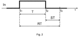
- the method for conversion of a time interval to a digital word using a successive approximation scheme consists in determining a difference between a length of a reference time RT and a length of a signal time ST ( Fig. 2 ).
- the reference time RT is generated from an instant t 1 when the beginning of the time interval T is detected by the use the control module CM.
- the signal time ST is generated from an instant t 2 when the end of the time interval T is detected by the use the control module CM.
- the generation of the reference time RT and the signal time ST is terminated at the same instant t 3 when each capacitor in the set of capacitors was charged.
- a binary representation of the difference between the length of the reference time RT and the length of the signal time ST is assigned by the control module to the n-bit output digital word B.
- the generation of the reference time RT is realized by charging a capacitor using a reference current source I R .
- This capacitor is selected by the use of the control module CM from a set of capacitors CS comprising capacitors C n-1 , C n-2 , ..., C 1 , Co.
- the capacitor C n-1 of the highest capacitance in the set of capacitors CS is selected first.
- a selected capacitor is charged as long as the reference voltage U R increasing on the selected capacitor and compared to the threshold voltage U TH by the use of the reference comparator K R reaches the threshold voltage U TH .
- a next capacitor in the set of capacitors CS is started to be charged while this capacitor has the highest capacitance among the capacitors that have not been charged yet, and the reference voltage U R increasing on this capacitor being charged is compared to the threshold voltage U TH by the use of the reference comparator K R .
- the cycle is repeated until all the capacitors C n-1 , C n-2 , ..., C 1 , Co are charged.
- Intensity of the reference current source I R and the signal current source Is are fixed and the same.
- the generation of the signal time ST is realized by charging a capacitor by the use of the signal current source Is.
- This capacitor selected by the use of the control module CM from a set of capacitors CS has the highest capacitance among the capacitors that have not been charged yet.
- the selected capacitor is charged as long as the signal voltage Us increasing on this capacitor and compared to the threshold voltage U TH by the use of the signal comparator Ks equals the threshold voltage U TH .
- a next capacitor in the set of capacitors CS is started to be charged by the use of the signal current source Is, while this capacitor is selected in the same way. The cycle is repeated until all the capacitors C n-1 , C n-2 , ..., C 1 , Co are charged.
- the generation of the reference time RT and the generation of the signal time ST are terminated during the time when the capacitor Co of the lowest capacitance in the set of capacitors CS is charged, and when the reference voltage U R increasing on a capacitor charged by the use of the reference current source I R , or when the signal voltage U R increasing on a capacitor charged by the use of the signal current source Is reaches the threshold voltage U TH .
- Another version of the method for conversion of a time interval to a digital word using a successive approximation scheme differs from the aforementioned version in that intensity of the reference current source I R is twice lower than intensity of the signal current source Is during the time interval T. Intensity of the reference current source I R is increased by the use of the control module CM to intensity of the signal current source Is at the instant t 2 when the generation of the time interval T is terminated by the use of the control module CM.
- a binary value represented by the n-bit output digital word B is evaluated by the use of the control module CM by subtracting a value of a second n-bit digital word from a value of a first n-bit digital word.
- a value one is assigned to bits of the first digital word if capacitors in the set of capacitors CS corresponding to these bits have been charged by the reference current source I R , and a value zero is assigned to other bits of the first digital word.
- Inverted values of the first digital word are assigned to corresponding bits of the second digital word by the use of the control module CM.
- the binary value of n-bit output digital word B is decreased by one if a voltage on the last capacitor charged by the reference current source I R has not reached the threshold voltage U TH .
- a binary value represented by the n-bit output digital word B is evaluated by the use of the control module CM such that the control module CM assigns a value one to a bit b j in this digital word if a next capacitor C j-i is not started to be charged by the use of the signal current source Is during a time when a capacitor C j corresponding to the bit b j in the set of capacitors CS is charged by the use of the reference current source I R , or a next capacitor C j-i is started to be charged by the use of the reference current source I R during a time when a capacitor C j is charged by the use of the signal current source Is.
- the control module CM assigns a value zero to the bit b j otherwise.
- an apparatus for conversion of a time interval to a digital word using a successive approximation scheme comprises a control module CM having a time input In, a digital output B, a complete conversion output RDY.
- a reference input In R of the control module CM is connected to an output of a reference comparator K R
- a signal input Ins of the control module CM is connected to an output of a signal comparator Ks ( Fig. 1 ).
- a reference output P R of the control module CM is connected to a control input of a reference current source I R
- a signal output Ps of the control module CM is connected to a control input of a signal current source Is.
- Control outputs P n-1 , P n-2 , ..., P 1 , Po of the control module CM are connected respectively to control inputs of change-over switches S n-1 , S n-2 , ..., S 1 , So of a set of capacitors CS.
- the inverting input of the signal comparator Ks is connected to the source of the threshold voltage U TH and to the inverting input of the reference comparator K R .
- Bottom plates of capacitors C n-1 , C n-2 , ..., C 1 , Co of the set of capacitors CS are connected to a ground of a circuit, and top plates of the capacitors C n-1 , C n-2 , ..., C 1 , Co are connected respectively to moving contacts of change-over switches S n-1 , S n-2 , ..., S 1 , So.
- First stationary contacts of the change-over switches S n-1 , S n-2 , ..., S 1 , So are connected to the signal rail S, second stationary contacts are connected to the ground of the circuit, and third stationary contacts are connected to the reference rail R.
- the signal current source Is and the reference current source I R have the same intensity in the first embodiment.
- the apparatus differs from the version presented in the first embodiment in that intensity of the reference current source I R is controllable, and is changed by the reference output P R of the control module CM.
- the control module CM causes the switching off the reference current source I R by the use of the signal from the reference output P R , and also the switching off the signal current source Is by the use of the signal from the signal output Ps. Additionally, by the use of signals from the control outputs P n-1 , P n-2 , ..., P 1 , P 0 , the control module CM causes the switching of change-over switches S n-1 , S n-2 , ..., S 1 , So and the connection of the top plates of the capacitors C n-1 , C n-2 , ..., C 1 , Co in the set of capacitors CS to the ground of the circuit enforcing a complete discharge of all the capacitors C n-1 , C n-2 , ..., C 1 , Co in the set of capacitors CS.
- the control module CM when the control module CM detects the beginning of the time interval T on the input time interval In, the control module CM introduces the complete conversion output RDY to an inactive state.
- the control module CM starts generation of the reference time RT ( Fig. 2 ).
- the control module CM causes the switching of the change-over switch S n-1 and the connection of an output of the reference current source I R to the top plate of the capacitor C n-1 having the highest capacitance in the set of capacitors CS.
- the control module CM causes the switching on the reference current source I R .
- control module assigns a value one to a bit b n-1 of the first n-bit digital word, and a value zero to a bit b n-1 of the second n-bit digital word.
- the reference voltage U R increasing on a capacitor C x charged by the use of the reference current source I R is compared to the threshold voltage U TH by the use of the reference comparator K R .
- the control module CM by the use of the signal from the control output P x causes the switching of the change-over switch S x and the connection of the top plate of the capacitor C x to the ground of the circuit enforcing a complete discharge of this capacitor.
- the control module CM by the use of the signal from the control output P z causes the switching of the change-over switch S z and the connection of the output of the reference current source I R to the top plate of the capacitor C z such that it has the highest capacitance among the capacitors CS in the set of capacitors that have not been charged yet.
- the control module assigns a value one to a bit b z of the first n-bit digital word, and a value zero to a bit b z of the second n-bit digital word.
- the reference voltage U R increasing on a capacitor C x charged by the use of the reference current source I R is compared to the threshold voltage U TH by the use of the reference comparator K R .
- the cycle is repeated until the generation of the reference time RT is terminated at the same instant t 3 .
- the control module CM detects the end of the time interval T on the input time interval In, the control module CM starts to generate the signal time ST ( Fig. 2 ).
- the control module CM causes the switching of the change-over switch S z and the connection of an output of the signal current source Is to the top plate of the capacitor C z such that it has the highest capacitance among the capacitors CS in the set of capacitors that have not been charged yet.
- the control module CM causes the switching on the signal current source Is.
- the control module assigns a value zero to a bit b n-1 of the first n-bit digital word, and a value one to a bit b n-1 of the second n-bit digital word.
- the signal voltage Us increasing on a capacitor C y charged by the use of the signal current source Is is compared to the threshold voltage U TH by the use of the signal comparator Ks.
- the control module CM by the use of the signal from the control output P y causes the switching of the change-over switch S y and the connection of the top plate of the capacitor C y to the ground of the circuit enforcing a complete discharge of this capacitor.
- control module CM by the use of the signal from the control output P z causes the switching of the change-over switch S z and the connection of the output of the signal current source Is to the top plate of the capacitor C z such that it has the highest capacitance among the capacitors CS in the set of capacitors that have not been charged yet.
- the cycle is repeated until generation of the signal time ST is terminated at the same instant t 3 .
- the generation of the reference time RT and the generation of the signal time ST are terminated by the control module CM at the instant t 3 ( Fig. 2 ) when the capacitor Co of the lowest capacitance in the set of capacitors CS is charged, and when the control module CM on the basis of the output signal of the reference comparator K R detects that the reference voltage U R increasing on a capacitor C x charged by the use of the reference current source I R equals the threshold voltage U TH , or when the control module CM on the basis of the output signal of the source comparator Ks detects that the signal voltage U s increasing on a capacitor C y charged by the use of the signal current source Is equals the threshold voltage U TH . In the latter case, the value of the first n-bit digital word is decreases by one by use of the control module CM.
- the control module CM by the use of the signal from the reference output Ps causes the switching off the reference current source I R and by the use of the signal from the signal output Ps causes the switching off the signal current source Is. Additionally, by the use of the signal from the control outputs P n-1 , P n-2 , ..., P 1 , P 0 , the control module CM causes the switching of the change-over switches S n-1 , S n-2 , ..., S 1 , So and the connection of the top plates of all the capacitors C n-1 , C n-2 , ..., C 1 , Co to the ground of the circuit enforcing a complete discharge of all the capacitors C n-1 , C n-2 , ..., C 1 , Co in the set of capacitors CS.
- the control module CM evaluates values of bits b n-1 , b n-2 , ..., b 1 , bo in the n-bit output digital word B subtracting a value of the second n-bit digital word from a value of the first n-bit digital word.
- the control module CM introduces the complete conversion output RDY to an active state.
- the apparatus for conversion of a time interval to a digital word using a successive approximation scheme differs from the version presented in aforementioned example in that the control module CM by the use of the control signal from the reference output P R causes a decrease of intensity of the reference current source I R below intensity of the signal current source Is at the instant t 1 , when the control module CM detects the beginning of the time interval T on the input time interval In.
- the control module CM by the use of the control signal from the reference output P R causes an increase of intensity of the reference current source I R to intensity of the signal current source Is.
- the control module CM evaluates values of bits b n-1 , b n-2 , ..., b 1 , bo in the n-bit output digital word B as a conversion result by assigning a value one to a bit b x in this digital word B if, a next capacitor C x-1 is not started to be charged by the use of the signal current source Is during a time when a capacitor C x corresponding to the bit b x in the set of capacitors CS is charged by the use of the reference current source I R , or, a next capacitor C y-1 is started to be charged by the use of the reference current source I R during a time when a capacitor C y corresponding to the bit b y in the set of capacitors CS is charged by the use of the signal current source Is. Otherwise, the control module CM assigns a value zero to the bits in this digital word B.
Landscapes
- Physics & Mathematics (AREA)
- General Physics & Mathematics (AREA)
- Engineering & Computer Science (AREA)
- Theoretical Computer Science (AREA)
- Analogue/Digital Conversion (AREA)
Applications Claiming Priority (2)
| Application Number | Priority Date | Filing Date | Title |
|---|---|---|---|
| PL413960A PL227451B1 (pl) | 2015-09-14 | 2015-09-14 | Sposób przetwarzania interwału czasu na słowo cyfrowe metodą kompensacji wagowej |
| PL413964A PL227455B1 (pl) | 2015-09-14 | 2015-09-14 | Układ do przetwarzania interwału czasu na słowo cyfrowe metodą kompensacji wagowej |
Publications (2)
| Publication Number | Publication Date |
|---|---|
| EP3141968A1 true EP3141968A1 (fr) | 2017-03-15 |
| EP3141968B1 EP3141968B1 (fr) | 2021-03-31 |
Family
ID=55068785
Family Applications (1)
| Application Number | Title | Priority Date | Filing Date |
|---|---|---|---|
| EP15200980.9A Active EP3141968B1 (fr) | 2015-09-14 | 2015-12-17 | Procédé et appareil de conversion d'intervalle de temps en mot numérique utilisant un schéma d'approximations successives |
Country Status (2)
| Country | Link |
|---|---|
| US (1) | US9612581B1 (fr) |
| EP (1) | EP3141968B1 (fr) |
Citations (2)
| Publication number | Priority date | Publication date | Assignee | Title |
|---|---|---|---|---|
| WO2011152744A2 (fr) | 2010-06-05 | 2011-12-08 | Akademia Gorniczo-Hutnicza Im. Stanislawa Staszica | Procédé et appareil pour conversion d'intervalle temporel en mot numérique |
| US20130207826A1 (en) * | 2012-01-31 | 2013-08-15 | Dariusz Koscielnik | Method and apparatus for clockless conversion of time interval to digital word |
Family Cites Families (1)
| Publication number | Priority date | Publication date | Assignee | Title |
|---|---|---|---|---|
| PL220448B1 (pl) * | 2012-01-31 | 2015-10-30 | Akademia Górniczo Hutnicza Im Stanisława Staszica W Krakowie | Sposób i układ do bezzegarowego przetwarzania chwilowej wielkości napięcia elektrycznego na słowo cyfrowe |
-
2015
- 2015-12-17 EP EP15200980.9A patent/EP3141968B1/fr active Active
- 2015-12-18 US US14/974,190 patent/US9612581B1/en active Active
Patent Citations (3)
| Publication number | Priority date | Publication date | Assignee | Title |
|---|---|---|---|---|
| WO2011152744A2 (fr) | 2010-06-05 | 2011-12-08 | Akademia Gorniczo-Hutnicza Im. Stanislawa Staszica | Procédé et appareil pour conversion d'intervalle temporel en mot numérique |
| US9063518B2 (en) | 2010-06-05 | 2015-06-23 | Akademia Gorniczo-Hutnicza Im. Stanislawa Staszica, Al. | Method and apparatus for conversion of time interval to digital word |
| US20130207826A1 (en) * | 2012-01-31 | 2013-08-15 | Dariusz Koscielnik | Method and apparatus for clockless conversion of time interval to digital word |
Also Published As
| Publication number | Publication date |
|---|---|
| US20170075311A1 (en) | 2017-03-16 |
| US9612581B1 (en) | 2017-04-04 |
| EP3141968B1 (fr) | 2021-03-31 |
Similar Documents
| Publication | Publication Date | Title |
|---|---|---|
| CN102386923B (zh) | 异步逐次逼近模数转换器及转换方法 | |
| KR102028266B1 (ko) | 정전용량형 지문 센서 | |
| US7969204B1 (en) | Sample hold circuit and method thereof for eliminating offset voltage of analog signal | |
| CN104410419A (zh) | 带有数字可编程选通窗的模数转换器 | |
| CN109792498B (zh) | 模数转换电路、图像传感器和模数转换方法 | |
| CN102640228A (zh) | 用于模数转换器的输入配置 | |
| US8928516B2 (en) | Method and apparatus for conversion of voltage value to digital word | |
| CN106656190A (zh) | 连续逼近式模拟数字转换电路及其方法 | |
| US9612581B1 (en) | Method and apparatus for conversion of time interval to digital word using successive approximation scheme | |
| CN109450449B (zh) | 参考电压控制电路和模数转换器 | |
| EP3145087B1 (fr) | Procédé et appareil de conversion indirecte de valeur de tension en mot numérique | |
| KR101768385B1 (ko) | 충전 시간을 이용한 최대전력지점 추적 기법을 적용한 에너지 하베스팅 시스템 | |
| US10084471B1 (en) | Analog to digital converter and wireless communication device | |
| JP2017026347A (ja) | 半導体装置、電池監視装置および電池セルの電圧検出方法 | |
| US9374101B2 (en) | Sensor device including high-resolution analog to digital converter | |
| Kościelnik et al. | A clockless time-to-digital converter | |
| KR102632360B1 (ko) | 병렬 카운팅 구조를 갖는 듀얼 슬로프 아날로그-디지털 변환기 | |
| US8922417B2 (en) | Method and apparatus for conversion of portion of electric charge to digital word | |
| CN108028660A (zh) | 用于对模数转换器的输入信号进行滤波的滤波器电路 | |
| US11757460B2 (en) | Analog-to-digital converter | |
| KR102028555B1 (ko) | 고해상도 아날로그-디지털 변환기를 포함하는 센서 장치 | |
| US20240162897A1 (en) | Delay apparatus and delay method | |
| PL227452B1 (pl) | Sposób pośredniego przetwarzania próbki napięcia elektrycznego na słowo cyfrowe | |
| JP2015186111A (ja) | アナログ‐デジタル変換装置 | |
| Kościelnik et al. | Analysis of conversion time of time-to-digital converters with charge redistribution |
Legal Events
| Date | Code | Title | Description |
|---|---|---|---|
| PUAI | Public reference made under article 153(3) epc to a published international application that has entered the european phase |
Free format text: ORIGINAL CODE: 0009012 |
|
| STAA | Information on the status of an ep patent application or granted ep patent |
Free format text: STATUS: THE APPLICATION HAS BEEN PUBLISHED |
|
| AK | Designated contracting states |
Kind code of ref document: A1 Designated state(s): AL AT BE BG CH CY CZ DE DK EE ES FI FR GB GR HR HU IE IS IT LI LT LU LV MC MK MT NL NO PL PT RO RS SE SI SK SM TR |
|
| AX | Request for extension of the european patent |
Extension state: BA ME |
|
| STAA | Information on the status of an ep patent application or granted ep patent |
Free format text: STATUS: REQUEST FOR EXAMINATION WAS MADE |
|
| 17P | Request for examination filed |
Effective date: 20170915 |
|
| GRAP | Despatch of communication of intention to grant a patent |
Free format text: ORIGINAL CODE: EPIDOSNIGR1 |
|
| STAA | Information on the status of an ep patent application or granted ep patent |
Free format text: STATUS: GRANT OF PATENT IS INTENDED |
|
| INTG | Intention to grant announced |
Effective date: 20201027 |
|
| GRAS | Grant fee paid |
Free format text: ORIGINAL CODE: EPIDOSNIGR3 |
|
| GRAA | (expected) grant |
Free format text: ORIGINAL CODE: 0009210 |
|
| STAA | Information on the status of an ep patent application or granted ep patent |
Free format text: STATUS: THE PATENT HAS BEEN GRANTED |
|
| AK | Designated contracting states |
Kind code of ref document: B1 Designated state(s): AL AT BE BG CH CY CZ DE DK EE ES FI FR GB GR HR HU IE IS IT LI LT LU LV MC MK MT NL NO PL PT RO RS SE SI SK SM TR |
|
| REG | Reference to a national code |
Ref country code: GB Ref legal event code: FG4D Ref country code: CH Ref legal event code: EP |
|
| REG | Reference to a national code |
Ref country code: AT Ref legal event code: REF Ref document number: 1377637 Country of ref document: AT Kind code of ref document: T Effective date: 20210415 |
|
| REG | Reference to a national code |
Ref country code: DE Ref legal event code: R096 Ref document number: 602015067419 Country of ref document: DE |
|
| REG | Reference to a national code |
Ref country code: IE Ref legal event code: FG4D |
|
| REG | Reference to a national code |
Ref country code: LT Ref legal event code: MG9D |
|
| PG25 | Lapsed in a contracting state [announced via postgrant information from national office to epo] |
Ref country code: NO Free format text: LAPSE BECAUSE OF FAILURE TO SUBMIT A TRANSLATION OF THE DESCRIPTION OR TO PAY THE FEE WITHIN THE PRESCRIBED TIME-LIMIT Effective date: 20210630 Ref country code: BG Free format text: LAPSE BECAUSE OF FAILURE TO SUBMIT A TRANSLATION OF THE DESCRIPTION OR TO PAY THE FEE WITHIN THE PRESCRIBED TIME-LIMIT Effective date: 20210630 Ref country code: FI Free format text: LAPSE BECAUSE OF FAILURE TO SUBMIT A TRANSLATION OF THE DESCRIPTION OR TO PAY THE FEE WITHIN THE PRESCRIBED TIME-LIMIT Effective date: 20210331 Ref country code: HR Free format text: LAPSE BECAUSE OF FAILURE TO SUBMIT A TRANSLATION OF THE DESCRIPTION OR TO PAY THE FEE WITHIN THE PRESCRIBED TIME-LIMIT Effective date: 20210331 |
|
| PG25 | Lapsed in a contracting state [announced via postgrant information from national office to epo] |
Ref country code: SE Free format text: LAPSE BECAUSE OF FAILURE TO SUBMIT A TRANSLATION OF THE DESCRIPTION OR TO PAY THE FEE WITHIN THE PRESCRIBED TIME-LIMIT Effective date: 20210331 Ref country code: RS Free format text: LAPSE BECAUSE OF FAILURE TO SUBMIT A TRANSLATION OF THE DESCRIPTION OR TO PAY THE FEE WITHIN THE PRESCRIBED TIME-LIMIT Effective date: 20210331 Ref country code: LV Free format text: LAPSE BECAUSE OF FAILURE TO SUBMIT A TRANSLATION OF THE DESCRIPTION OR TO PAY THE FEE WITHIN THE PRESCRIBED TIME-LIMIT Effective date: 20210331 |
|
| REG | Reference to a national code |
Ref country code: NL Ref legal event code: MP Effective date: 20210331 |
|
| REG | Reference to a national code |
Ref country code: AT Ref legal event code: MK05 Ref document number: 1377637 Country of ref document: AT Kind code of ref document: T Effective date: 20210331 |
|
| PG25 | Lapsed in a contracting state [announced via postgrant information from national office to epo] |
Ref country code: SM Free format text: LAPSE BECAUSE OF FAILURE TO SUBMIT A TRANSLATION OF THE DESCRIPTION OR TO PAY THE FEE WITHIN THE PRESCRIBED TIME-LIMIT Effective date: 20210331 Ref country code: AT Free format text: LAPSE BECAUSE OF FAILURE TO SUBMIT A TRANSLATION OF THE DESCRIPTION OR TO PAY THE FEE WITHIN THE PRESCRIBED TIME-LIMIT Effective date: 20210331 Ref country code: NL Free format text: LAPSE BECAUSE OF FAILURE TO SUBMIT A TRANSLATION OF THE DESCRIPTION OR TO PAY THE FEE WITHIN THE PRESCRIBED TIME-LIMIT Effective date: 20210331 Ref country code: LT Free format text: LAPSE BECAUSE OF FAILURE TO SUBMIT A TRANSLATION OF THE DESCRIPTION OR TO PAY THE FEE WITHIN THE PRESCRIBED TIME-LIMIT Effective date: 20210331 Ref country code: CZ Free format text: LAPSE BECAUSE OF FAILURE TO SUBMIT A TRANSLATION OF THE DESCRIPTION OR TO PAY THE FEE WITHIN THE PRESCRIBED TIME-LIMIT Effective date: 20210331 Ref country code: EE Free format text: LAPSE BECAUSE OF FAILURE TO SUBMIT A TRANSLATION OF THE DESCRIPTION OR TO PAY THE FEE WITHIN THE PRESCRIBED TIME-LIMIT Effective date: 20210331 |
|
| PG25 | Lapsed in a contracting state [announced via postgrant information from national office to epo] |
Ref country code: ES Free format text: LAPSE BECAUSE OF FAILURE TO SUBMIT A TRANSLATION OF THE DESCRIPTION OR TO PAY THE FEE WITHIN THE PRESCRIBED TIME-LIMIT Effective date: 20210331 Ref country code: PT Free format text: LAPSE BECAUSE OF FAILURE TO SUBMIT A TRANSLATION OF THE DESCRIPTION OR TO PAY THE FEE WITHIN THE PRESCRIBED TIME-LIMIT Effective date: 20210802 Ref country code: PL Free format text: LAPSE BECAUSE OF FAILURE TO SUBMIT A TRANSLATION OF THE DESCRIPTION OR TO PAY THE FEE WITHIN THE PRESCRIBED TIME-LIMIT Effective date: 20210331 Ref country code: SK Free format text: LAPSE BECAUSE OF FAILURE TO SUBMIT A TRANSLATION OF THE DESCRIPTION OR TO PAY THE FEE WITHIN THE PRESCRIBED TIME-LIMIT Effective date: 20210331 Ref country code: RO Free format text: LAPSE BECAUSE OF FAILURE TO SUBMIT A TRANSLATION OF THE DESCRIPTION OR TO PAY THE FEE WITHIN THE PRESCRIBED TIME-LIMIT Effective date: 20210331 Ref country code: IS Free format text: LAPSE BECAUSE OF FAILURE TO SUBMIT A TRANSLATION OF THE DESCRIPTION OR TO PAY THE FEE WITHIN THE PRESCRIBED TIME-LIMIT Effective date: 20210731 |
|
| REG | Reference to a national code |
Ref country code: DE Ref legal event code: R097 Ref document number: 602015067419 Country of ref document: DE |
|
| PG25 | Lapsed in a contracting state [announced via postgrant information from national office to epo] |
Ref country code: AL Free format text: LAPSE BECAUSE OF FAILURE TO SUBMIT A TRANSLATION OF THE DESCRIPTION OR TO PAY THE FEE WITHIN THE PRESCRIBED TIME-LIMIT Effective date: 20210331 Ref country code: DK Free format text: LAPSE BECAUSE OF FAILURE TO SUBMIT A TRANSLATION OF THE DESCRIPTION OR TO PAY THE FEE WITHIN THE PRESCRIBED TIME-LIMIT Effective date: 20210331 |
|
| PGFP | Annual fee paid to national office [announced via postgrant information from national office to epo] |
Ref country code: FR Payment date: 20211220 Year of fee payment: 7 Ref country code: DE Payment date: 20211220 Year of fee payment: 7 Ref country code: GB Payment date: 20211222 Year of fee payment: 7 |
|
| PLBE | No opposition filed within time limit |
Free format text: ORIGINAL CODE: 0009261 |
|
| STAA | Information on the status of an ep patent application or granted ep patent |
Free format text: STATUS: NO OPPOSITION FILED WITHIN TIME LIMIT |
|
| 26N | No opposition filed |
Effective date: 20220104 |
|
| PG25 | Lapsed in a contracting state [announced via postgrant information from national office to epo] |
Ref country code: IS Free format text: LAPSE BECAUSE OF FAILURE TO SUBMIT A TRANSLATION OF THE DESCRIPTION OR TO PAY THE FEE WITHIN THE PRESCRIBED TIME-LIMIT Effective date: 20210731 |
|
| PG25 | Lapsed in a contracting state [announced via postgrant information from national office to epo] |
Ref country code: MC Free format text: LAPSE BECAUSE OF FAILURE TO SUBMIT A TRANSLATION OF THE DESCRIPTION OR TO PAY THE FEE WITHIN THE PRESCRIBED TIME-LIMIT Effective date: 20210331 Ref country code: IT Free format text: LAPSE BECAUSE OF FAILURE TO SUBMIT A TRANSLATION OF THE DESCRIPTION OR TO PAY THE FEE WITHIN THE PRESCRIBED TIME-LIMIT Effective date: 20210331 |
|
| REG | Reference to a national code |
Ref country code: CH Ref legal event code: PL |
|
| REG | Reference to a national code |
Ref country code: BE Ref legal event code: MM Effective date: 20211231 |
|
| PG25 | Lapsed in a contracting state [announced via postgrant information from national office to epo] |
Ref country code: LU Free format text: LAPSE BECAUSE OF NON-PAYMENT OF DUE FEES Effective date: 20211217 Ref country code: IE Free format text: LAPSE BECAUSE OF NON-PAYMENT OF DUE FEES Effective date: 20211217 |
|
| PG25 | Lapsed in a contracting state [announced via postgrant information from national office to epo] |
Ref country code: BE Free format text: LAPSE BECAUSE OF NON-PAYMENT OF DUE FEES Effective date: 20211231 |
|
| PG25 | Lapsed in a contracting state [announced via postgrant information from national office to epo] |
Ref country code: LI Free format text: LAPSE BECAUSE OF NON-PAYMENT OF DUE FEES Effective date: 20211231 Ref country code: CH Free format text: LAPSE BECAUSE OF NON-PAYMENT OF DUE FEES Effective date: 20211231 |
|
| PG25 | Lapsed in a contracting state [announced via postgrant information from national office to epo] |
Ref country code: HU Free format text: LAPSE BECAUSE OF FAILURE TO SUBMIT A TRANSLATION OF THE DESCRIPTION OR TO PAY THE FEE WITHIN THE PRESCRIBED TIME-LIMIT; INVALID AB INITIO Effective date: 20151217 |
|
| PG25 | Lapsed in a contracting state [announced via postgrant information from national office to epo] |
Ref country code: CY Free format text: LAPSE BECAUSE OF FAILURE TO SUBMIT A TRANSLATION OF THE DESCRIPTION OR TO PAY THE FEE WITHIN THE PRESCRIBED TIME-LIMIT Effective date: 20210331 |
|
| REG | Reference to a national code |
Ref country code: DE Ref legal event code: R119 Ref document number: 602015067419 Country of ref document: DE |
|
| PG25 | Lapsed in a contracting state [announced via postgrant information from national office to epo] |
Ref country code: GR Free format text: LAPSE BECAUSE OF FAILURE TO SUBMIT A TRANSLATION OF THE DESCRIPTION OR TO PAY THE FEE WITHIN THE PRESCRIBED TIME-LIMIT Effective date: 20210331 |
|
| GBPC | Gb: european patent ceased through non-payment of renewal fee |
Effective date: 20221217 |
|
| PG25 | Lapsed in a contracting state [announced via postgrant information from national office to epo] |
Ref country code: GB Free format text: LAPSE BECAUSE OF NON-PAYMENT OF DUE FEES Effective date: 20221217 Ref country code: DE Free format text: LAPSE BECAUSE OF NON-PAYMENT OF DUE FEES Effective date: 20230701 |
|
| PG25 | Lapsed in a contracting state [announced via postgrant information from national office to epo] |
Ref country code: FR Free format text: LAPSE BECAUSE OF NON-PAYMENT OF DUE FEES Effective date: 20221231 |
|
| PG25 | Lapsed in a contracting state [announced via postgrant information from national office to epo] |
Ref country code: MK Free format text: LAPSE BECAUSE OF FAILURE TO SUBMIT A TRANSLATION OF THE DESCRIPTION OR TO PAY THE FEE WITHIN THE PRESCRIBED TIME-LIMIT Effective date: 20210331 |