EP3139551A1 - Distributed multi-die protocol application interface - Google Patents
Distributed multi-die protocol application interface Download PDFInfo
- Publication number
- EP3139551A1 EP3139551A1 EP16187034.0A EP16187034A EP3139551A1 EP 3139551 A1 EP3139551 A1 EP 3139551A1 EP 16187034 A EP16187034 A EP 16187034A EP 3139551 A1 EP3139551 A1 EP 3139551A1
- Authority
- EP
- European Patent Office
- Prior art keywords
- circuit
- fifo
- data streams
- data
- die
- Prior art date
- Legal status (The legal status is an assumption and is not a legal conclusion. Google has not performed a legal analysis and makes no representation as to the accuracy of the status listed.)
- Granted
Links
Images


Classifications
-
- H—ELECTRICITY
- H04—ELECTRIC COMMUNICATION TECHNIQUE
- H04L—TRANSMISSION OF DIGITAL INFORMATION, e.g. TELEGRAPHIC COMMUNICATION
- H04L12/00—Data switching networks
- H04L12/28—Data switching networks characterised by path configuration, e.g. LAN [Local Area Networks] or WAN [Wide Area Networks]
- H04L12/40—Bus networks
- H04L12/40052—High-speed IEEE 1394 serial bus
- H04L12/40091—Bus bridging
-
- G—PHYSICS
- G06—COMPUTING OR CALCULATING; COUNTING
- G06F—ELECTRIC DIGITAL DATA PROCESSING
- G06F13/00—Interconnection of, or transfer of information or other signals between, memories, input/output devices or central processing units
- G06F13/38—Information transfer, e.g. on bus
- G06F13/42—Bus transfer protocol, e.g. handshake; Synchronisation
- G06F13/4282—Bus transfer protocol, e.g. handshake; Synchronisation on a serial bus, e.g. I2C bus, SPI bus
- G06F13/4286—Bus transfer protocol, e.g. handshake; Synchronisation on a serial bus, e.g. I2C bus, SPI bus using a handshaking protocol, e.g. RS232C link
-
- G—PHYSICS
- G06—COMPUTING OR CALCULATING; COUNTING
- G06F—ELECTRIC DIGITAL DATA PROCESSING
- G06F5/00—Methods or arrangements for data conversion without changing the order or content of the data handled
- G06F5/06—Methods or arrangements for data conversion without changing the order or content of the data handled for changing the speed of data flow, i.e. speed regularising or timing, e.g. delay lines, FIFO buffers; over- or underrun control therefor
- G06F5/065—Partitioned buffers, e.g. allowing multiple independent queues, bidirectional FIFO's
-
- H—ELECTRICITY
- H04—ELECTRIC COMMUNICATION TECHNIQUE
- H04L—TRANSMISSION OF DIGITAL INFORMATION, e.g. TELEGRAPHIC COMMUNICATION
- H04L12/00—Data switching networks
- H04L12/28—Data switching networks characterised by path configuration, e.g. LAN [Local Area Networks] or WAN [Wide Area Networks]
- H04L12/40—Bus networks
- H04L12/40052—High-speed IEEE 1394 serial bus
- H04L12/40123—Interconnection of computers and peripherals
-
- H—ELECTRICITY
- H04—ELECTRIC COMMUNICATION TECHNIQUE
- H04L—TRANSMISSION OF DIGITAL INFORMATION, e.g. TELEGRAPHIC COMMUNICATION
- H04L69/00—Network arrangements, protocols or services independent of the application payload and not provided for in the other groups of this subclass
- H04L69/14—Multichannel or multilink protocols
-
- H—ELECTRICITY
- H04—ELECTRIC COMMUNICATION TECHNIQUE
- H04L—TRANSMISSION OF DIGITAL INFORMATION, e.g. TELEGRAPHIC COMMUNICATION
- H04L49/00—Packet switching elements
- H04L49/25—Routing or path finding in a switch fabric
Definitions
- This invention relates to multi-die integrated circuit devices, including programmable logic devices (PLD).
- PLD programmable logic devices
- this invention can be used in systems and methods for supporting multi-purpose signaling on such devices.
- IC dies can be connected using a multi-die interconnect.
- the multi-die interconnect can be implemented as a channelized interface, where multiple channels are used to relay data signals among the multiple IC dies.
- a protocol application layer stack can reside on one or more of the IC dies that are connected via the multi-die interconnect. In some modes, communication between two protocol application layer stacks is accomplished by way of the multi-die interconnect interface.
- the present invention describes a clean way of supporting multi-purpose data signaling across a channelized interface such as the multi-die interconnect.
- several channels of the multi-die interconnect can be aggregated to support a wide-protocol bus interface from the protocol application layer.
- multi-die interconnects are typically implemented as narrow, independent, and asynchronous channels.
- Parallel data bits in a wide-protocol bus interface must be divided and redistributed across different channels of the multi-die interconnect in order to be transmitted.
- the asynchronous first-in-first-out devices (FIFOs) that are used to drive channels of the multi-die interconnect interface have the potential to introduce skew into the data streams because the channels operate independently and asynchronously of each other.
- a method for supporting a wide-protocol interface across a multi-die interconnect Data signals of the wide-protocol interface are split into a plurality of data streams.
- a handshake signal is established between a first circuit and a second circuit residing on IC dies of a multi-die device.
- the first circuit transmits the plurality of data streams to the second circuit via a plurality of channels of the multi-die interconnect interface.
- the plurality of channels of the multi-die interconnect interface may be "bonded" by shared synchronization signals in order to reduce skew in the plurality of data streams.
- Each data stream of the plurality of data streams is compressed based on the handshake signal in order to provide a wide-protocol interface with a reduced number of required pins.
- a first data stream of the plurality of data streams is driven through a first FIFO at a 2:1 speed-up rate and through a second FIFO at a 1:2 slow-down rate.
- a second data stream of the plurality of data streams is driven through a third FIFO at a 2:1 speed-up rate and through a fourth FIFO at a 1:2 slow-down rate.
- the first FIFO and the third FIFO are bonded by a first pair of shared synchronization signals
- the second FIFO and the fourth FIFO are bonded by a second pair of shared synchronization signals.
- capacity remaining in a protocol layer FIFO is determined, and a back-pressure latency associated with the first FIFO and the second FIFO also is determined based on the handshake signal. In some embodiments, the capacity remaining in the protocol layer FIFO is adjusted based on the determined back-pressure latency.
- the handshake signal is established between the first circuit and the second circuit via a serial-shift chain.
- control signals associated with the data signals of the wide-protocol interface are collected and split across the plurality of data streams.
- FIG. 1 shows a circuit diagram of a multi-die interconnect interface across two IC dies.
- Multi-die device 100 may include main die 120 and secondary die 140, which are in communication with each other via a multi-die interconnect.
- the multi-die interconnect may be implemented as a channelized interface.
- the channelized multi-die interconnect interface may include multi-die interconnect interface (MDII) 130 (e.g., MDII0, MDII1,... MDIIN of FIG. 1 ) and multi-die interconnect channels (MDIC) 150.
- MDII multi-die interconnect interface
- MDIC multi-die interconnect channels
- the channelized multi-die interconnect interface can, for example, be the 2.5D multi-die interface available from Altera Corporation, of San Jose, California, and can be implemented on both main die 120 and secondary die 140.
- Data signals communicated on a channel of MDIC 150 may herein be referred to as a stream of data signals, or a data stream.
- a programmable logic device (PLD) fabric such as PLD fabric 122, can be implemented on main die 120.
- a number of transceiver channels 142 can be implemented on secondary die 140.
- channelized paths 146, MDIC 150, and channelized paths 126 transceiver channels 142 on secondary die 140 can be bridged into PLD fabric 122 on main die 120.
- the channelized multi-die interconnect interface (MDII 130 and MDIC 150) is defined to be a per-channel interconnect (e.g., 96 pins per channel) in order to allow transceiver channels 142 to be bridged into PLD fabric 122.
- channel 7 (e.g., XCV7) of transceiver channels 142 may have a one-to-one relationship with a channel of the channelized multi-die interconnect interface, such as MDII7, when the transceiver channel is bridged into PLD fabric 122.
- the channelized multi-die interconnect interface is a bidirectional interface.
- the 96 pins per channel in the MDIC 150 can operate in both the main-to-secondary direction and the secondary-to-main direction.
- protocol application layer stack 144 such as Peripheral Component Interconnect Express (PCIe) stack, and its application interface can also be provided on secondary die 140 in order for secondary die 140 to engage in protocol application layer communication directly with protocol application layer 124 on main die 120.
- protocol application layer 124 requires a wide communication bus (e.g., over 1,200 pins), such as non-channelized paths 128 and 148.
- Each channel of MDIC 150 can support three different classes of data signals:
- the source-synchronous data is data that arrives at a deterministic time and that includes a clock signal (a "strobe") which is independent of the receiving system clock.
- Source-synchronous data transfers can often attain higher transfer rates than a scheme that implements global clock source topology.
- the high-speed TDM interface handles synchronous transfers of memory-mapped data between a source and a sink (e.g., a protocol layer FIFO and an interconnect interface FIFO on secondary die 140).
- a protocol layer FIFO and an interconnect interface FIFO on secondary die 140 e.g., a protocol layer FIFO and an interconnect interface FIFO on secondary die 140.
- application interface Tx FIFO 246 is a protocol layer FIFO
- multi-die interconnect interface Tx FIFO 230n is an interconnect interface FIFO.
- serial-shift chain 260 of FIG. 2 allows asynchronous handshake signals (e.g., a "transfer ready” signal or a "FIFO empty” flag) to be communicated between the protocol stack and a PLD fabric application logic so that proper communication of parallel data can be established prior to any communication occurs on the FIFO blocks.
- asynchronous handshake signals e.g., a "transfer ready” signal or a "FIFO empty” flag
- the protocol stack 144 utilizes the existing channelized multi-die interconnect interface (MDII 130 and MDIC 150) in order to bridge its non-channelized application interface into main die 120.
- the non-channelized application interface may require a wide communication bus (e.g., over 1200 pins) whereas, in the example shown, each channel of MDIC 150 may have a relatively small bandwidth (e.g., 96 pins). Consequently, the pin count limitation of the channelized multi-die interconnect interface may require secondary die 140 to communicate protocol application layer data with main die 120 across multiple channels in MDIC 150.
- a particular channel e.g., MDII7 of FIG.
- MDIC 150 some or all of the other channels in MDIC 150 may lose their capability to perform other functions.
- a PCIe x1 lane uses only one transceiver; however, its corresponding PCIe protocol stack may require sixteen channels in MDIC 150 in order to function. The user would thus lose fifteen transceiver channels that could have been used for other purposes, because all sixteen channels of transceiver interface 142 would become unavailable to other modules whenever protocol stack 144 is enabled.
- the present invention can reduce the number of channels in the channelized multi-die interconnect interface that are utilized to implement a protocol application layer communication.
- MDII 130 and MDIC 150 Another issue with data communication on channelized interfaces (e.g., MDII 130 and MDIC 150) arises from the fact that these channels are, by nature, asynchronous. MDII 130 and MDIC 150 may introduce skew to a wide bus of data driven through each independent asynchronous interconnect FIFO within the channelized interface. The present invention can reduce or eliminate skew in the middle of the wide bus of data transmitted via MDIC 150.
- each die on multi-die device 100 may have an independent reset interface, and therefore may be configured to wake up at different times due to their varying reset periods. Any data signals exchanged between main die 120 and secondary die 140 prior to the end of both reset periods are indeterminate. Accordingly, data communication should be gated until both dies have exited the reset period.
- FIG. 1 discusses an exemplary multi-die device where a multi-die interconnect is needed for protocol application layer communication.
- a number of existing issues and design challenges are also laid out, for which solutions will be presented below in relation to FIG. 2 .
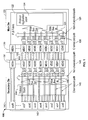
- FIG. 2 shows an implementation of circuit channels in the multi-die interconnect interface in accordance with an embodiment of the invention. More specifically, FIG. 2 includes circuit diagram 200 which shows implementation details of certain elements of multi-die device 100 as described in relation to FIG. 1 .
- FIG. 2 includes main die 220 and secondary die 240, which correspond to main die 120 and secondary die 140, respectively.
- a number of multi-die interconnect interface FIFOs such as multi-die interconnect interface Tx (MITx) FIFOs 232a..232n and multi-die interconnect interface Rx (MIRx) FIFOs 234a..234n, reside on main die 220. Although only two MITx FIFOs and MIRx FIFOs are shown in FIG. 2 , any number of such FIFOs may be implemented without deviating from the scope of the present invention.
- Protocol stack 244 substantially corresponds to protocol stack 144 of FIG. 1 .
- Transceiver channels 242a..242n substantially correspond to transceiver channels 142 of FIG. 1 .
- the multi-die interconnect interface FIFOs implemented on both main die 220 and secondary die 240, as well as serial-shift chain 260, are circuit level implementations of the channelized multi-die interconnect interface (i.e., MDII 130 and MDIC 150) of FIG. 1 .
- Protocol stack 244 implemented on secondary die 240 may be in communication with two protocol layer FIFOs: application interface transmit (AITx) FIFO 246 and application interface receive (AIRx) FIFO 248.
- AITx FIFO 246 receives data signals from MITx FIFOs 230a..230n to relay to protocol stack 244, whereas AIRx FIFO 248 transmits data signals from protocol stack 244 to MIRx FIFOs 236a..236n.
- the protocol layer FIFOs 246 and 248 may be referred to as a source and the multi-die interconnect interface FIFOs 230 and 236 may be referred to as a sink for the interface shown in FIG. 2 .
- protocol stack 244 requires a wide synchronous protocol data bus (e.g., 256-bit) for communication with protocol application layer logic implemented on PLD fabric 122.
- the synchronous protocol data bus is associated with a number of control pins, such as Start-of-Packet (SOP), End-of-Packet (EOP), Valid, and Ready.
- SOP is asserted by the source to mark the beginning of a packet.
- EOP is asserted by the source to mark the end of a packet.
- Valid is asserted by the source to qualify all other source-to-sink signals.
- the sink samples source-to-sink signals only on cycles where Valid is asserted; all other cycles are ignored.
- Ready is asserted by the sink to indicate that the sink can accept data.
- the source may only assert Valid and transfer data during Ready cycles.
- data channels in multi-die interconnect channels 150 may introduce skew because the data channels operate independently of each other.
- multiple channels in the channelized multi-die interconnect interface may be bonded together by a synchronization signal (e.g., the read/write enable signal of each FIFO block in the multi-die interconnect interface).
- the synchronization signal can be passed along FIFO bonding connection 238.
- data and control pins e.g., SOP, EOP, Ready, Valid, etc. as discussed before
- MDII 130 and MDIC 150 Any number of data channels in the multi-die interconnect interface may be bonded together. In this manner, the unused data channels can be used for other functions, or be repurposed for other protocol application layer communications.
- Transceiver channels 242a..242n may be coupled with the interconnect FIFOs by way of multiplexing units in order to receive and transmit source-synchronous data.
- each transceiver channel may be in communication with one or more MITx FIFOs 230a..230n to receive data, and with one or more MIRx FIFOs 236a..236n to transmit data.
- Transceiver phase-locked loop (PLL) 210 can be implemented on multi-die device 100 to provide different clock signals to the multi-die communication interface.
- transceiver PLL 210 may provide two clock signals: a PLL fixed clock 212 and a PLL fixed clock 2X 214.
- PLL fixed clock 2X 214 runs at substantially twice the rate of PLL fixed clock 212.
- PLL fixed clock 212 may optionally be subdivided to generate protocol clock signal 211 and interconnect 1x clock signal 213.
- PLL fixed clock 2x 214 may optionally be subdivided to generate interconnect 2x clock signal 215.
- Protocol clock signal 211 is used to drive the operation of the protocol layer FIFOs (e.g., AITx FIFO 246 and AIRx FIFO 248).
- Interconnect 1x clock signal 213 and interconnect 2x clock signal 215 are collectively used to facilitate the interconnect FIFOs on both main die 220 and secondary die 240 to support data pin compression and phase compensation.
- the interconnect FIFOs operate in a phase compensation mode, with a 2:1 speed-up implemented across the channels in multi-die interconnect channels 150.
- the 2:1 speed-up is initiated by MITx FIFOs 232a..232n on main die 220 and MIRx FIFOs 236a..236n on secondary die 240, using the 2x relationship between interconnect 1x clock signal 213 and interconnect 2x clock signal 215.
- MITx FIFOs 230a..230n on secondary die 240 and MIRx FIFOs 234a..234n implements a 1:2 slow-down.
- the 2:1 speed-up and the 1:2 slow-down are used to minimize the number of required pins for a given wide bus communication, and require a 2x clock (e.g., interconnect 1x clock signal 213 and interconnect 2x clock signal 215) to drive the source-synchronous interconnect transfer.
- a 2x clock e.g., interconnect 1x clock signal 213 and interconnect 2x clock signal 215
- the interconnect FIFOs with the 2x (i.e., 2:1) speed-up appear as an extra latency in the protocol path.
- the source e.g., protocol FIFOs
- the sink e.g., interconnect FIFOs 150
- the Ready->Valid back-pressure latency indicates the number of cycles from the time that Ready is asserted until Valid data can be driven.
- the protocol layer FIFOs e.g., AITx FIFO 246 and AIRx FIFO 248, should have enough space to account for the increased Ready->Valid back-pressure latency.
- circuit diagram 200 may also include serial-shift chain 260.
- Various user control status information such as the FIFO empty flag, may be communicated across serial-shift chain 260 in order to initialize the IC dies prior to data communications commence on the channels of multi-die interconnect interface.
- a method according to an embodiment of the present invention for implementing a multi-die interconnect between two IC dies of a multi-die device is diagrammed in FIG. 3 .
- data signals of a wide-protocol interface are split into a plurality of data streams.
- a handshake signal is established between a first circuit and a second circuit.
- control signals e.g., the handshake signal
- gate the interface signals until both dies have exited their respective reset periods.
- additional control (handshake) signals govern the handshaking process between the two dies (e.g., main die 220 and secondary die 240), such that the Ready and Valid signals are set only at the appropriate moment.
- an asynchronous serial-shift chain (e.g., serial-shift chain 260) is required to pass control (handshake) information between the two dies.
- the plurality of data streams are transmitted from the first circuit to the second circuit via a plurality of channels of the multi-die interconnect interface.
- each data stream of the plurality of data streams is compressed based on the handshake signal.
- FIFO bonding may be achieved by running a shared synchronization signal through multiple asynchronous FIFO blocks.
- a first FIFO block e.g. MITx FIFO 230n
- the synchronization signal can be fed into other FIFO blocks (e.g., MIRx FIFO 236n and MITx FIFO 230a) by way of FIFO bonding 238.
- the synchronization signal controls the read/write enables of the parallel asynchronous FIFO blocks.
- the asynchronous FIFO blocks which reside on independent and parallel channels of the multi-die interconnect interface, can operate in a synchronized manner to carry data streams across IC dies, thereby eliminating skew, as caused by the independent asynchronous resets, on the data streams.
- serial-shift chains such as serial-shift chain 260
- serial-shift chain 260 can provide an alternate path for asynchronous control and handshaking signals (e.g., FIFO empty flag), which should be established prior to the data streams are transmitted via the FIFO blocks.
- Serial-shift chain 260 employs an independent oscillator to oversample the asynchronous control and handshaking signals in order to initialize both IC dies.
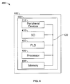
- FIG. 4 illustrates a circuit or other device 402 that includes embodiments of a circuitry designed or configured based on the model described herein within a data processing system 400.
- integrated circuit or device 402 may be an integrated circuit, application specific standard product (ASSP), application specific integrated circuit (ASIC), programmable logic device (PLD) (including a Field-Programmable Gate Array (FPGA), full-custom chip, or a dedicated chip).
- element 402 may be configured as multi-die device 100, main die 120, or secondary die 140.
- Data processing system 400 may include one or more of the following components: circuit 402, processor 406, memory 408, I/O circuitry 410, and peripheral devices 412. These components are connected together by a system bus or other interconnections 420 and are populated on a circuit board 430 which is contained in an end-user system 440.
- System 400 could be used in a wide variety of applications, such as communications, computer networking, data networking, instrumentation, video processing, digital signal processing, or any other application where the advantage of using programmable or reprogrammable logic is desirable.
- Circuit 402 may be used to perform a variety of different logic functions.
- circuit 402 may be configured as a processor or controller that works in cooperation with processor 406.
- Circuit 402 may also be used as an arbiter for arbitrating access to a shared resource in system 400.
- circuit 402 can be configured as an interface between processor 406 and one of the other components in system 400. It should be noted that system 400 is only exemplary.
- Instructions for carrying out a method according to this invention for programming a programmable device to implement a multi-die interconnect interface may be encoded on a machine-readable medium, to be executed by a suitable computer or similar device to implement the method of the invention for programming or configuring PLDs or other programmable devices.
- a personal computer may be equipped with an interface to which a PLD can be connected, and the personal computer can be used by a user to program the PLD using suitable software tools as described above
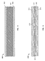
- FIG. 5 presents a cross section of a magnetic data storage medium 500 which can be encoded with a machine executable program that can be carried out by systems such as the aforementioned personal computer, or other computer or similar device.
- Medium 500 can be a floppy diskette or hard disk, or magnetic tape, having a suitable substrate 501, which may be conventional, and a suitable coating 502, which may be conventional, on one or both sides, containing magnetic domains (not visible) whose polarity or orientation can be altered magnetically. Except in the case where it is magnetic tape, medium 500 may also have an opening (not shown) for receiving the spindle of a disk drive or other data storage device.
- the magnetic domains of coating 502 of medium 100 are polarized or oriented so as to encode, in manner which may be conventional, a machine-executable program, for execution by a programming system such as a personal computer or other computer or similar system, having a socket or peripheral attachment into which the PLD to be programmed may be inserted, to configure appropriate portions of the PLD, including its specialized processing blocks, if any, in accordance with the invention.
- FIG. 6 shows a cross section of an optically-readable data storage medium 510 which also can be encoded with such a machine-executable program, which can be carried out by systems such as the aforementioned personal computer, or other computer or similar device.
- Medium 510 can be a conventional compact disk read-only memory (CD-ROM) or digital video disk read-only memory (DVD-ROM) or a rewriteable medium such as a CD-R, CD-RW, DVD-R, DVD-RW, DVD+R, DVD+RW, or DVD-RAM or a magneto-optical disk which is optically readable and magneto-optically rewriteable.
- Medium 510 preferably has a suitable substrate 511, which may be conventional, and a suitable coating 512, which may be conventional, usually on one or both sides of substrate 511.
- coating 512 is reflective and is impressed with a plurality of pits 513, arranged on one or more layers, to encode the machine-executable program.
- the arrangement of pits is read by reflecting laser light off the surface of coating 512.
- a protective coating 514 which preferably is substantially transparent, is provided on top of coating 1512.
- coating 512 has no pits 513, but has a plurality of magnetic domains whose polarity or orientation can be changed magnetically when heated above a certain temperature, as by a laser (not shown).
- the orientation of the domains can be read by measuring the polarization of laser light reflected from coating 512.
- the arrangement of the domains encodes the program as described above.
- Embodiment 1 A method of configuring a programmable logic device comprising a first circuit and a second circuit, the method comprising:
- Additional Embodiment 2 The method of Additional Embodiment 1, wherein configuring the plurality of FIFO blocks further comprises:
- Additional Embodiment 3 The method of Additional Embodiment 2, further comprising
- Additional Embodiment 4 The method of Additional Embodiment 2 or 3, further comprising:
- Additional Embodiment 5 The method of one of Additional Embodiments 2-4, wherein the first circuit and the second circuit are dies of a multi-die device.
- Additional Embodiment 6 The method of one of Additional Embodiments 2-5, comprising:
- Embodiment 7 A non-transitory machine-readable storage medium encoded with instructions for performing a method of configuring a programmable integrated circuit device having a first circuit and a second circuit, the instructions comprising:
- Additional Embodiment 8 The non-transitory machine-readable storage medium of Additional Embodiment 7, wherein the instructions to configure the plurality of FIFO blocks further comprise:
- Additional Embodiment 9 The non-transitory machine-readable storage of Additional Embodiment 8, wherein the instructions further comprise instructions to bond the plurality of multi-die interconnect channels to reduce skew in the plurality of data streams.
- Additional Embodiment 10 The non-transitory machine-readable storage of one of Additional Embodiments 7-9, wherein the instructions further comprise instructions to configure the second circuit to:
- Additional Embodiment 11 The non-transitory machine-readable storage of one of Additional Embodiments 7-10, wherein the instructions further comprise instructions to configure the first circuit to:
Landscapes
- Engineering & Computer Science (AREA)
- Theoretical Computer Science (AREA)
- General Engineering & Computer Science (AREA)
- Computer Networks & Wireless Communication (AREA)
- Signal Processing (AREA)
- Physics & Mathematics (AREA)
- General Physics & Mathematics (AREA)
- Computer Security & Cryptography (AREA)
- Computer Hardware Design (AREA)
- Information Transfer Systems (AREA)
- Communication Control (AREA)
- Bus Control (AREA)
- Semiconductor Integrated Circuits (AREA)
- Logic Circuits (AREA)
Abstract
Description
- This invention relates to multi-die integrated circuit devices, including programmable logic devices (PLD). In particular, this invention can be used in systems and methods for supporting multi-purpose signaling on such devices.
- Multiple integrated circuit (IC) dies can be connected using a multi-die interconnect. In some examples, the multi-die interconnect can be implemented as a channelized interface, where multiple channels are used to relay data signals among the multiple IC dies.
- A protocol application layer stack can reside on one or more of the IC dies that are connected via the multi-die interconnect. In some modes, communication between two protocol application layer stacks is accomplished by way of the multi-die interconnect interface.
- The present invention describes a clean way of supporting multi-purpose data signaling across a channelized interface such as the multi-die interconnect. In some implementations, several channels of the multi-die interconnect can be aggregated to support a wide-protocol bus interface from the protocol application layer.
- A particular challenge in supporting the wide-protocol bus interface across multiple IC dies is that multi-die interconnects are typically implemented as narrow, independent, and asynchronous channels. Parallel data bits in a wide-protocol bus interface must be divided and redistributed across different channels of the multi-die interconnect in order to be transmitted. Furthermore, the asynchronous first-in-first-out devices (FIFOs) that are used to drive channels of the multi-die interconnect interface have the potential to introduce skew into the data streams because the channels operate independently and asynchronously of each other.
- Therefore, in accordance with embodiments of the present invention, there is provided a method for supporting a wide-protocol interface across a multi-die interconnect. Data signals of the wide-protocol interface are split into a plurality of data streams. A handshake signal is established between a first circuit and a second circuit residing on IC dies of a multi-die device. The first circuit transmits the plurality of data streams to the second circuit via a plurality of channels of the multi-die interconnect interface. The plurality of channels of the multi-die interconnect interface may be "bonded" by shared synchronization signals in order to reduce skew in the plurality of data streams. Each data stream of the plurality of data streams is compressed based on the handshake signal in order to provide a wide-protocol interface with a reduced number of required pins.
- While each data stream of the plurality of data streams is compressed, a first data stream of the plurality of data streams is driven through a first FIFO at a 2:1 speed-up rate and through a second FIFO at a 1:2 slow-down rate. A second data stream of the plurality of data streams is driven through a third FIFO at a 2:1 speed-up rate and through a fourth FIFO at a 1:2 slow-down rate. In some embodiments, the first FIFO and the third FIFO are bonded by a first pair of shared synchronization signals, and the second FIFO and the fourth FIFO are bonded by a second pair of shared synchronization signals.
- In some embodiments, capacity remaining in a protocol layer FIFO is determined, and a back-pressure latency associated with the first FIFO and the second FIFO also is determined based on the handshake signal. In some embodiments, the capacity remaining in the protocol layer FIFO is adjusted based on the determined back-pressure latency.
- In some embodiments, the handshake signal is established between the first circuit and the second circuit via a serial-shift chain. In some further embodiments, control signals associated with the data signals of the wide-protocol interface are collected and split across the plurality of data streams.
- Further features of the invention, its nature and various advantages will be apparent upon consideration of the following detailed description, taken in conjunction with the accompanying drawings, in which like referenced characters refer to like parts throughout, and in which:
-
FIG. 1 shows a circuit diagram of a multi-die interconnect interface across two IC dies in accordance with an embodiment of the invention; -
FIG. 2 shows an implementation of circuit channels in the multi-die interconnect interface in accordance with an embodiment of the invention; -
FIG. 3 is a flow diagram of a method according to an embodiment of the present invention for implementing a multi-die interconnect interface between two IC dies of a multi-die device; -
FIG. 4 is a simplified block diagram of an illustrative system employing an integrated circuit device in accordance with an embodiment of the present invention; -
FIG. 5 is a cross-sectional view of a magnetic data storage medium encoded with a set of machine-executable instructions for performing the method according to the present invention for configuring a programmable integrated circuit device to implement multi-die interconnect; and -
FIG. 6 is a cross-sectional view of an optically readable data storage medium encoded with a set of machine executable instructions for performing the method according to the present invention for configuring a programmable integrated circuit device to implement multi-die interconnect. - To provide an overall understanding of the invention, certain illustrative embodiments will now be described. However, it will be understood by one of ordinary skill in the art that the systems and methods described herein may be adapted and modified as is appropriate for the application being addressed and that the systems and methods described herein may be employed in other suitable applications, and that such other additions and modifications will not depart from the scope hereof.
- The drawings described herein show illustrative embodiments; however, the drawings may not necessarily show and may not be intended to show the exact layout of the hardware components contained in the embodiments. The embodiments disclosed herein may be implemented with any suitable number of components and any suitable layout of components in accordance with principles known in the art.
-
FIG. 1 shows a circuit diagram of a multi-die interconnect interface across two IC dies.Multi-die device 100 may include main die 120 andsecondary die 140, which are in communication with each other via a multi-die interconnect. The multi-die interconnect may be implemented as a channelized interface. For example, the channelized multi-die interconnect interface may include multi-die interconnect interface (MDII) 130 (e.g., MDII0, MDII1,... MDIIN ofFIG. 1 ) and multi-die interconnect channels (MDIC) 150. The channelized multi-die interconnect interface can, for example, be the 2.5D multi-die interface available from Altera Corporation, of San Jose, California, and can be implemented on bothmain die 120 andsecondary die 140. Data signals communicated on a channel of MDIC 150 may herein be referred to as a stream of data signals, or a data stream. The channelized multi-die interconnect interface is capable of supporting multiple data streams concurrently. - A programmable logic device (PLD) fabric, such as
PLD fabric 122, can be implemented on main die 120. A number oftransceiver channels 142 can be implemented onsecondary die 140. By way of channelizedpaths 146, MDIC 150, and channelizedpaths 126,transceiver channels 142 onsecondary die 140 can be bridged intoPLD fabric 122 onmain die 120. In some embodiments, the channelized multi-die interconnect interface (MDII 130 and MDIC 150) is defined to be a per-channel interconnect (e.g., 96 pins per channel) in order to allowtransceiver channels 142 to be bridged intoPLD fabric 122. For example, channel 7 (e.g., XCV7) oftransceiver channels 142 may have a one-to-one relationship with a channel of the channelized multi-die interconnect interface, such as MDII7, when the transceiver channel is bridged intoPLD fabric 122. In some embodiments, the channelized multi-die interconnect interface is a bidirectional interface. For example, the 96 pins per channel in the MDIC 150 can operate in both the main-to-secondary direction and the secondary-to-main direction. - In addition to
transceiver channels 142, a protocolapplication layer stack 144, such as Peripheral Component Interconnect Express (PCIe) stack, and its application interface can also be provided onsecondary die 140 in order forsecondary die 140 to engage in protocol application layer communication directly withprotocol application layer 124 on main die 120. In some embodiments,protocol application layer 124 requires a wide communication bus (e.g., over 1,200 pins), such as non-channelizedpaths - Each channel of MDIC 150 can support three different classes of data signals:
- 1) source-synchronous data;
- 2) memory-mapped data used, e.g., in a high-speed time-domain multiplexed (TDM) interface; and
- 3) asynchronous out-of-band data signals as used in a serial-shift chain.
- These three classes of data signals may be implemented differently and serve different functions. The source-synchronous data is data that arrives at a deterministic time and that includes a clock signal (a "strobe") which is independent of the receiving system clock. Source-synchronous data transfers can often attain higher transfer rates than a scheme that implements global clock source topology. The high-speed TDM interface handles synchronous transfers of memory-mapped data between a source and a sink (e.g., a protocol layer FIFO and an interconnect interface FIFO on secondary die 140). For example, as will be illustrated in relation to
FIG. 2 , applicationinterface Tx FIFO 246 is a protocol layer FIFO and multi-die interconnectinterface Tx FIFO 230n is an interconnect interface FIFO. Lastly, the asynchronous serial-shift chain, such as serial-shift chain 260 ofFIG. 2 , allows asynchronous handshake signals (e.g., a "transfer ready" signal or a "FIFO empty" flag) to be communicated between the protocol stack and a PLD fabric application logic so that proper communication of parallel data can be established prior to any communication occurs on the FIFO blocks. - The
protocol stack 144 utilizes the existing channelized multi-die interconnect interface (MDII 130 and MDIC 150) in order to bridge its non-channelized application interface intomain die 120. As discussed above, the non-channelized application interface may require a wide communication bus (e.g., over 1200 pins) whereas, in the example shown, each channel ofMDIC 150 may have a relatively small bandwidth (e.g., 96 pins). Consequently, the pin count limitation of the channelized multi-die interconnect interface may requiresecondary die 140 to communicate protocol application layer data withmain die 120 across multiple channels inMDIC 150. However, whenever a particular channel (e.g., MDII7 ofFIG. 1 ) is being used for a protocol application layer communication, some or all of the other channels inMDIC 150 may lose their capability to perform other functions. For example, a PCIe x1 lane uses only one transceiver; however, its corresponding PCIe protocol stack may require sixteen channels inMDIC 150 in order to function. The user would thus lose fifteen transceiver channels that could have been used for other purposes, because all sixteen channels oftransceiver interface 142 would become unavailable to other modules wheneverprotocol stack 144 is enabled. The present invention can reduce the number of channels in the channelized multi-die interconnect interface that are utilized to implement a protocol application layer communication. - Another issue with data communication on channelized interfaces (e.g.,
MDII 130 and MDIC 150) arises from the fact that these channels are, by nature, asynchronous.MDII 130 andMDIC 150 may introduce skew to a wide bus of data driven through each independent asynchronous interconnect FIFO within the channelized interface. The present invention can reduce or eliminate skew in the middle of the wide bus of data transmitted viaMDIC 150. - Lastly, each die on
multi-die device 100 may have an independent reset interface, and therefore may be configured to wake up at different times due to their varying reset periods. Any data signals exchanged betweenmain die 120 andsecondary die 140 prior to the end of both reset periods are indeterminate. Accordingly, data communication should be gated until both dies have exited the reset period. - The foregoing disclosure in relation to
FIG. 1 discusses an exemplary multi-die device where a multi-die interconnect is needed for protocol application layer communication. A number of existing issues and design challenges are also laid out, for which solutions will be presented below in relation toFIG. 2 . -
FIG. 2 shows an implementation of circuit channels in the multi-die interconnect interface in accordance with an embodiment of the invention. More specifically,FIG. 2 includes circuit diagram 200 which shows implementation details of certain elements ofmulti-die device 100 as described in relation toFIG. 1 .FIG. 2 includesmain die 220 andsecondary die 240, which correspond tomain die 120 andsecondary die 140, respectively. - A number of multi-die interconnect interface FIFOs, such as multi-die interconnect interface Tx (MITx) FIFOs 232a..232n and multi-die interconnect interface Rx (MIRx) FIFOs 234a..234n, reside on
main die 220. Although only two MITx FIFOs and MIRx FIFOs are shown inFIG. 2 , any number of such FIFOs may be implemented without deviating from the scope of the present invention. - On
secondary die 240, aprotocol stack 244,transceiver channels 242a..242n, as well as a number of MITx FIFOs 230a..230n andMIRx FIFO 236a..236n are implemented.Protocol stack 244 substantially corresponds toprotocol stack 144 ofFIG. 1 .Transceiver channels 242a..242n substantially correspond to transceiverchannels 142 ofFIG. 1 . The multi-die interconnect interface FIFOs implemented on bothmain die 220 andsecondary die 240, as well as serial-shift chain 260, are circuit level implementations of the channelized multi-die interconnect interface (i.e.,MDII 130 and MDIC 150) ofFIG. 1 . -
Protocol stack 244 implemented onsecondary die 240 may be in communication with two protocol layer FIFOs: application interface transmit (AITx)FIFO 246 and application interface receive (AIRx)FIFO 248.AITx FIFO 246 receives data signals from MITx FIFOs 230a..230n to relay toprotocol stack 244, whereasAIRx FIFO 248 transmits data signals fromprotocol stack 244 to MIRx FIFOs 236a..236n. As previously illustrated in relation toFIG. 1 , theprotocol layer FIFOs FIG. 2 . - In an exemplary embodiment,
protocol stack 244 requires a wide synchronous protocol data bus (e.g., 256-bit) for communication with protocol application layer logic implemented onPLD fabric 122. The synchronous protocol data bus is associated with a number of control pins, such as Start-of-Packet (SOP), End-of-Packet (EOP), Valid, and Ready. SOP is asserted by the source to mark the beginning of a packet. EOP is asserted by the source to mark the end of a packet. Valid is asserted by the source to qualify all other source-to-sink signals. The sink samples source-to-sink signals only on cycles where Valid is asserted; all other cycles are ignored. Lastly, Ready is asserted by the sink to indicate that the sink can accept data. The source may only assert Valid and transfer data during Ready cycles. - As previously discussed in relation to
FIG. 1 , data channels inmulti-die interconnect channels 150 may introduce skew because the data channels operate independently of each other. To resolve this issue and eliminate the skew in the data bus, multiple channels in the channelized multi-die interconnect interface may be bonded together by a synchronization signal (e.g., the read/write enable signal of each FIFO block in the multi-die interconnect interface). In some embodiments, the synchronization signal can be passed alongFIFO bonding connection 238. - As a result of the synchronized operation of these otherwise asynchronous and independent data channels, data and control pins (e.g., SOP, EOP, Ready, Valid, etc. as discussed before) can be distributed across multiple channels of the multi-die interconnect interface, because the multiple channels are effectively bonded into a same bundle. Any number of data channels in the multi-die interconnect interface (i.e.,
MDII 130 and MDIC 150) may be bonded together. In this manner, the unused data channels can be used for other functions, or be repurposed for other protocol application layer communications. -
Transceiver channels 242a..242n may be coupled with the interconnect FIFOs by way of multiplexing units in order to receive and transmit source-synchronous data. In the absence of protocol application layer communications, each transceiver channel may be in communication with one or more MITx FIFOs 230a..230n to receive data, and with one or more MIRx FIFOs 236a..236n to transmit data. - Transceiver phase-locked loop (PLL) 210 can be implemented on
multi-die device 100 to provide different clock signals to the multi-die communication interface. In particular, transceiver PLL 210 may provide two clock signals: a PLL fixedclock 212 and a PLL fixedclock 2X 214. PLL fixedclock 2X 214 runs at substantially twice the rate of PLL fixedclock 212. - PLL fixed
clock 212 may optionally be subdivided to generateprotocol clock signal 211 and interconnect1x clock signal 213. PLL fixedclock 2xinterconnect 2x clock signal 215.Protocol clock signal 211 is used to drive the operation of the protocol layer FIFOs (e.g.,AITx FIFO 246 and AIRx FIFO 248). Interconnect1x clock signal 213 andinterconnect 2x clock signal 215 are collectively used to facilitate the interconnect FIFOs on bothmain die 220 andsecondary die 240 to support data pin compression and phase compensation. - The interconnect FIFOs operate in a phase compensation mode, with a 2:1 speed-up implemented across the channels in
multi-die interconnect channels 150. The 2:1 speed-up is initiated by MITx FIFOs 232a..232n onmain die 220 and MIRx FIFOs 236a..236n onsecondary die 240, using the 2x relationship between interconnect1x clock signal 213 andinterconnect 2x clock signal 215. At the other end of the channels inmulti-die interconnect channels 150, MITx FIFOs 230a..230n onsecondary die 240 and MIRx FIFOs 234a..234n implements a 1:2 slow-down. The 2:1 speed-up and the 1:2 slow-down are used to minimize the number of required pins for a given wide bus communication, and require a 2x clock (e.g., interconnect1x clock signal 213 andinterconnect 2x clock signal 215) to drive the source-synchronous interconnect transfer. In some embodiments, the interconnect FIFOs with the 2x (i.e., 2:1) speed-up appear as an extra latency in the protocol path. - As discussed above, the source (e.g., protocol FIFOs) may only assert Valid and transfer data during Ready cycles as asserted by the sink (e.g., interconnect FIFOs 150). The Ready->Valid back-pressure latency indicates the number of cycles from the time that Ready is asserted until Valid data can be driven. As a result of the extra latency due to the 2x speed-up across the interconnect FIFOs, the protocol layer FIFOs (e.g.,
AITx FIFO 246 and AIRx FIFO 248) should have enough space to account for the increased Ready->Valid back-pressure latency. - In addition to
protocol stack 244 and the FIFOs, circuit diagram 200 may also include serial-shift chain 260. Various user control status information, such as the FIFO empty flag, may be communicated across serial-shift chain 260 in order to initialize the IC dies prior to data communications commence on the channels of multi-die interconnect interface. - A method according to an embodiment of the present invention for implementing a multi-die interconnect between two IC dies of a multi-die device is diagrammed in
FIG. 3 . At 310, data signals of a wide-protocol interface are split into a plurality of data streams. At 320, a handshake signal is established between a first circuit and a second circuit. In some embodiments, control signals (e.g., the handshake signal) gate the interface signals until both dies have exited their respective reset periods. During normal operation, additional control (handshake) signals govern the handshaking process between the two dies (e.g.,main die 220 and secondary die 240), such that the Ready and Valid signals are set only at the appropriate moment. In some embodiments, an asynchronous serial-shift chain (e.g., serial-shift chain 260) is required to pass control (handshake) information between the two dies. At 330, the plurality of data streams are transmitted from the first circuit to the second circuit via a plurality of channels of the multi-die interconnect interface. At 340, each data stream of the plurality of data streams is compressed based on the handshake signal. - As previously discussed, the plurality of channels of the multi-die interconnect interface are bonded in order to reduce skew in the plurality of data streams. FIFO bonding may be achieved by running a shared synchronization signal through multiple asynchronous FIFO blocks. For example, a first FIFO block (
e.g. MITx FIFO 230n) may be a master block that generates a synchronization signal. The synchronization signal can be fed into other FIFO blocks (e.g.,MIRx FIFO 236n andMITx FIFO 230a) by way ofFIFO bonding 238. In some embodiments, the synchronization signal controls the read/write enables of the parallel asynchronous FIFO blocks. In this manner, the asynchronous FIFO blocks, which reside on independent and parallel channels of the multi-die interconnect interface, can operate in a synchronized manner to carry data streams across IC dies, thereby eliminating skew, as caused by the independent asynchronous resets, on the data streams. - As previously illustrated, serial-shift chains, such as serial-
shift chain 260, can provide an alternate path for asynchronous control and handshaking signals (e.g., FIFO empty flag), which should be established prior to the data streams are transmitted via the FIFO blocks. Serial-shift chain 260 employs an independent oscillator to oversample the asynchronous control and handshaking signals in order to initialize both IC dies. - Thus it is seen that a system and a method for implementing a multi-die interconnect between two IC dies have been provided.
-
FIG. 4 illustrates a circuit orother device 402 that includes embodiments of a circuitry designed or configured based on the model described herein within adata processing system 400. In an embodiment, integrated circuit ordevice 402 may be an integrated circuit, application specific standard product (ASSP), application specific integrated circuit (ASIC), programmable logic device (PLD) (including a Field-Programmable Gate Array (FPGA), full-custom chip, or a dedicated chip). In some embodiments,element 402 may be configured asmulti-die device 100,main die 120, orsecondary die 140.Data processing system 400 may include one or more of the following components:circuit 402,processor 406,memory 408, I/O circuitry 410, andperipheral devices 412. These components are connected together by a system bus orother interconnections 420 and are populated on acircuit board 430 which is contained in an end-user system 440. -
System 400 could be used in a wide variety of applications, such as communications, computer networking, data networking, instrumentation, video processing, digital signal processing, or any other application where the advantage of using programmable or reprogrammable logic is desirable.Circuit 402 may be used to perform a variety of different logic functions. In some embodiments,circuit 402 may be configured as a processor or controller that works in cooperation withprocessor 406.Circuit 402 may also be used as an arbiter for arbitrating access to a shared resource insystem 400. In yet another example,circuit 402 can be configured as an interface betweenprocessor 406 and one of the other components insystem 400. It should be noted thatsystem 400 is only exemplary. - Although components in the above invention are described as being connected with one another, they may instead be connected to one another, possibly via other components in between them. It will be understood that the foregoing are only illustrative of the principles of the invention, and that various modifications can be made by those skilled in the art. One skilled in the art will appreciate that the present invention can be practiced by other than the described embodiments, which are presented for purposes of illustration and not of limitation.
- Instructions for carrying out a method according to this invention for programming a programmable device to implement a multi-die interconnect interface may be encoded on a machine-readable medium, to be executed by a suitable computer or similar device to implement the method of the invention for programming or configuring PLDs or other programmable devices. For example, a personal computer may be equipped with an interface to which a PLD can be connected, and the personal computer can be used by a user to program the PLD using suitable software tools as described above
-
FIG. 5 presents a cross section of a magneticdata storage medium 500 which can be encoded with a machine executable program that can be carried out by systems such as the aforementioned personal computer, or other computer or similar device. Medium 500 can be a floppy diskette or hard disk, or magnetic tape, having asuitable substrate 501, which may be conventional, and asuitable coating 502, which may be conventional, on one or both sides, containing magnetic domains (not visible) whose polarity or orientation can be altered magnetically. Except in the case where it is magnetic tape, medium 500 may also have an opening (not shown) for receiving the spindle of a disk drive or other data storage device. - The magnetic domains of
coating 502 ofmedium 100 are polarized or oriented so as to encode, in manner which may be conventional, a machine-executable program, for execution by a programming system such as a personal computer or other computer or similar system, having a socket or peripheral attachment into which the PLD to be programmed may be inserted, to configure appropriate portions of the PLD, including its specialized processing blocks, if any, in accordance with the invention. -
FIG. 6 shows a cross section of an optically-readabledata storage medium 510 which also can be encoded with such a machine-executable program, which can be carried out by systems such as the aforementioned personal computer, or other computer or similar device. Medium 510 can be a conventional compact disk read-only memory (CD-ROM) or digital video disk read-only memory (DVD-ROM) or a rewriteable medium such as a CD-R, CD-RW, DVD-R, DVD-RW, DVD+R, DVD+RW, or DVD-RAM or a magneto-optical disk which is optically readable and magneto-optically rewriteable.Medium 510 preferably has asuitable substrate 511, which may be conventional, and asuitable coating 512, which may be conventional, usually on one or both sides ofsubstrate 511. - In the case of a CD-based or DVD-based medium, as is well known, coating 512 is reflective and is impressed with a plurality of
pits 513, arranged on one or more layers, to encode the machine-executable program. The arrangement of pits is read by reflecting laser light off the surface ofcoating 512. Aprotective coating 514, which preferably is substantially transparent, is provided on top of coating 1512. - In the case of magneto-optical disk, as is well known, coating 512 has no
pits 513, but has a plurality of magnetic domains whose polarity or orientation can be changed magnetically when heated above a certain temperature, as by a laser (not shown). The orientation of the domains can be read by measuring the polarization of laser light reflected fromcoating 512. The arrangement of the domains encodes the program as described above. - It will be understood that the foregoing is only illustrative of the principles of the invention, and that various modifications may be made by those skilled in the art. For example, the various inventive aspects that have been discussed herein can either all be used together in certain embodiments, or other embodiments may employ only one or more (but less than all) of the inventive aspects. And if multiple (but less than all) of the inventive aspects are employed, that can involve employment of any combination of the inventive aspects. As another example of possible modifications, throughout this invention, particular numbers of components used in controllers are mentioned. These particular numbers are only examples, and other suitable parameter values can be used instead if desired. Additional nonlimiting examples follow.
- CERTAIN EXAMPLE EMBODIMENTS
- Additional Embodiment 1: A method of configuring a programmable logic device comprising a first circuit and a second circuit, the method comprising:
- configuring a serial-shift chain to establish a handshake signal between the first circuit and the second circuit;
- configuring the first circuit to split data signals of a wide-protocol interface into a plurality of data streams; and
- configuring a plurality of multi-die interconnect first-in-first-out (FIFO) blocks on the first circuit and the second circuit to:
- transmit a plurality of data streams from the first circuit to the second circuit; and
- compress each data stream of the plurality of data streams based on the handshake signal.
- Additional Embodiment 2: The method of
Additional Embodiment 1, wherein configuring the plurality of FIFO blocks further comprises: - configuring the plurality of FIFO blocks to drive a first data stream of the plurality of data streams through a first FIFO block at a 2:1 speed-up rate and a second FIFO block at a 1:2 slow-down rate; and
- configuring the plurality of FIFO blocks to drive a second data stream of the plurality of data streams through a third FIFO block at a 2:1 speed-up rate and a fourth FIFO block at a 1:2 slow-down rate.A method of configuring a programmable logic
- Additional Embodiment 3: The method of
Additional Embodiment 2, further comprising - configuring the first FIFO block to bond with the third FIFO block in order to reduce skew in the plurality of data streams; and
- configuring the second FIFO block to bond with the fourth FIFO block in order to reduce skew in the plurality of data streams.
- Additional Embodiment 4: The method of
Additional Embodiment 2 or 3, further comprising: - configuring the second circuit to determine capacity remaining in a protocol layer FIFO;
- configuring the second circuit to determine a back-pressure latency associated with the first FIFO and the second FIFO based on the handshake signal; and
- configuring the second circuit to adjust the capacity remaining in the protocol layer FIFO based on the back-pressure latency.
- Additional Embodiment 5: The method of one of Additional Embodiments 2-4, wherein the first circuit and the second circuit are dies of a multi-die device.
- Additional Embodiment 6: The method of one of Additional Embodiments 2-5, comprising:
- configuring the first circuit to collect control signals associated with the data signals of the wide-protocol interface; and
- configuring the first circuit to split the control signals across the plurality of data streams.
- Additional Embodiment 7: A non-transitory machine-readable storage medium encoded with instructions for performing a method of configuring a programmable integrated circuit device having a first circuit and a second circuit, the instructions comprising:
- instructions to configure a serial-shift chain to establish a handshake signal between the first circuit and the second circuit;
- instructions to configure the first circuit to split data signals of a wide-protocol interface into a plurality of data streams; and
- instructions to configure a plurality of multi-die interconnect first-in-first-out (FIFO) blocks on the first circuit and the second circuit to:
- transmit a plurality of data streams from the first circuit to the second circuit; and
- compress each data stream of the plurality of data streams based on the handshake signal.
- Additional Embodiment 8: The non-transitory machine-readable storage medium of Additional Embodiment 7, wherein the instructions to configure the plurality of FIFO blocks further comprise:
- instructions to configure the plurality of FIFO blocks to drive a first data stream of the plurality of data streams through a first FIFO block at a 2:1 speed-up rate and a second FIFO block at a 1:2 slow-down rate; and
- instructions to configure the plurality of FIFO blocks to drive a second data stream of the plurality of data streams through a third FIFO block at a 2:1 speed-up rate and a fourth FIFO block at a 1:2 slow-down rate.
- Additional Embodiment 9: The non-transitory machine-readable storage of Additional Embodiment 8, wherein the instructions further comprise instructions to bond the plurality of multi-die interconnect channels to reduce skew in the plurality of data streams.
- Additional Embodiment 10: The non-transitory machine-readable storage of one of Additional Embodiments 7-9, wherein the instructions further comprise instructions to configure the second circuit to:
- determine capacity remaining in a protocol layer FIFO;
- determine a back-pressure latency associated with the first FIFO and the second FIFO based on the handshake signal; and
- adjust the capacity remaining in the protocol layer FIFO based on the back-pressure latency.
- Additional Embodiment 11: The non-transitory machine-readable storage of one of Additional Embodiments 7-10, wherein the instructions further comprise instructions to configure the first circuit to:
- collect control signals associated with the data signals of the wide-protocol interface; and
- split the control signals across the plurality of data streams.
Claims (15)
- A method for supporting a wide-protocol interface across a multi-die interconnect having a plurality of channels, the method comprising:splitting data signals of the wide-protocol interface into a plurality of data streams;establishing a handshake signal between a first circuit and a second circuit;transmitting, from the first circuit, the plurality of data streams to the second circuit via the plurality of channels of the multi-die interconnect; andcompressing each data stream of the plurality of data streams based on the handshake signal.
- The method of claim 1, wherein compressing the each data stream of the plurality of data streams further comprises:driving a first data stream of the plurality of data streams through a first first-in-first-out (FIFO) block at a 2:1 speed-up rate and a second FIFO block at a 1:2 slow-down rate; anddriving a second data stream of the plurality of data streams through a third FIFO block at a 2:1 speed-up rate and a fourth FIFO block at a 1:2 slow-down rate.
- The method of claim 2, further comprising bonding the plurality of multi-die interconnect channels to reduce skew in the plurality of data streams by bonding the first FIFO block with the third FIFO block and by bonding the second FIFO block with the fourth FIFO block.
- The method of claims 2 or 3, further comprising:determining capacity remaining in a protocol layer FIFO;determining a back-pressure latency associated with the first FIFO block and the second FIFO block based on the handshake signal; andadjusting the capacity remaining in the protocol layer FIFO based on the back-pressure latency.
- The method of one of claims 1-4, wherein establishing the handshake signal between the first circuit and the second circuit further comprises transmitting and receiving the handshake signal via a serial-shift chain.
- The method of one of claims 1-5, wherein the first circuit and the second circuit are dies of a multi-die device.
- The method of one of claims 1-6, further comprising:collecting control signals associated with the data signals of the wide-protocol interface; andsplitting the control signals across the plurality of data streams.
- An integrated circuit multi-die device, comprising:a first circuit comprising a wide-protocol interface, the first circuit configured to split data signals of the wide-protocol interface into a plurality of data streams;a second circuit comprising a programmable logic fabric;a serial-shift chain configured to establish a handshake signal between the first circuit and the second circuit; anda plurality of multi-die interconnect first-in-first-out (FIFO) blocks configured to:transmit the plurality of data streams from the first circuit to the second circuit; andcompress each data stream of the plurality of data streams based on the handshake signal.
- The integrated circuit of claim 8, wherein the plurality of multi-die interconnect FIFO blocks is further configured to:drive a first data stream of the plurality of data streams through a first FIFO block at a 2:1 speed-up rate and a second FIFO block at a 1:2 slow-down rate; anddrive a second data stream of the plurality of data streams through a third FIFO block at a 2:1 speed-up rate and a fourth FIFO block at a 1:2 slow-down rate.
- The integrated circuit of claim 9, wherein the plurality of multi-die interconnect FIFO blocks are further configured to bond the first FIFO block with the third FIFO block and to bond the second FIFO block with the fourth FIFO block in order to reduce skew in the plurality of data streams.
- The integrated circuit of claims 9 or 10, wherein the second circuit is further configured to:determine capacity remaining in a protocol layer FIFO block;determine a back-pressure latency associated with the first FIFO block and the second FIFO block based on the handshake signal; andadjust the capacity remaining in the protocol layer FIFO block based on the back-pressure latency.
- The integrated circuit of one of claims 8-11, wherein the first circuit and the second circuit are dies of a multi-die device.
- The integrated circuit of one of claims 8-12, wherein the first circuit is further configured to:collect control signals associated with the data signals of the wide-protocol interface; andsplit the control signals across the plurality of data streams
- The integrated circuit of one of claims 8-13, wherein the second circuit comprises an application specific integrated circuit.
- The integrated circuit of one of claims 8-13, wherein the second circuit comprises programmable logic fabric, wherein the serial-shift chain configured to establish the handshake signal between the first circuit and the second circuit is implemented at least in part using the programmable logic fabric of the second circuit.
Applications Claiming Priority (1)
| Application Number | Priority Date | Filing Date | Title |
|---|---|---|---|
| US14/844,920 US10162789B2 (en) | 2015-09-03 | 2015-09-03 | Distributed multi-die protocol application interface |
Publications (2)
| Publication Number | Publication Date |
|---|---|
| EP3139551A1 true EP3139551A1 (en) | 2017-03-08 |
| EP3139551B1 EP3139551B1 (en) | 2018-03-07 |
Family
ID=56936275
Family Applications (1)
| Application Number | Title | Priority Date | Filing Date |
|---|---|---|---|
| EP16187034.0A Active EP3139551B1 (en) | 2015-09-03 | 2016-09-02 | Distributed multi-die protocol application interface |
Country Status (3)
| Country | Link |
|---|---|
| US (6) | US10162789B2 (en) |
| EP (1) | EP3139551B1 (en) |
| CN (2) | CN106549843B (en) |
Cited By (1)
| Publication number | Priority date | Publication date | Assignee | Title |
|---|---|---|---|---|
| WO2022072027A1 (en) * | 2020-09-29 | 2022-04-07 | Xilinx, Inc. | Communication between integrated circuit (1c) dies in wafer- level fan-out package |
Families Citing this family (5)
| Publication number | Priority date | Publication date | Assignee | Title |
|---|---|---|---|---|
| US10344204B2 (en) | 2015-04-09 | 2019-07-09 | Diversion Technologies, LLC | Gas diverter for well and reservoir stimulation |
| US10012064B2 (en) | 2015-04-09 | 2018-07-03 | Highlands Natural Resources, Plc | Gas diverter for well and reservoir stimulation |
| US10162789B2 (en) * | 2015-09-03 | 2018-12-25 | Altera Corporation | Distributed multi-die protocol application interface |
| US10982520B2 (en) | 2016-04-27 | 2021-04-20 | Highland Natural Resources, PLC | Gas diverter for well and reservoir stimulation |
| KR102315325B1 (en) | 2017-07-05 | 2021-10-19 | 삼성전자주식회사 | Semiconductor package |
Citations (2)
| Publication number | Priority date | Publication date | Assignee | Title |
|---|---|---|---|---|
| US20100215086A1 (en) * | 2008-10-17 | 2010-08-26 | Altera Corporation | Multi-protocol channel-aggregated configurable transceiver in an integrated circuit |
| US20120027026A1 (en) * | 2010-07-28 | 2012-02-02 | Keith Duwel | Scalable interconnect modules with flexible channel bonding |
Family Cites Families (19)
| Publication number | Priority date | Publication date | Assignee | Title |
|---|---|---|---|---|
| US6006318A (en) * | 1995-08-16 | 1999-12-21 | Microunity Systems Engineering, Inc. | General purpose, dynamic partitioning, programmable media processor |
| US6188699B1 (en) * | 1997-12-11 | 2001-02-13 | Pmc-Sierra Ltd. | Multi-channel encoder/decoder |
| EP1313163B1 (en) * | 2001-11-14 | 2006-05-03 | Marconi Communications GmbH | Multichip module |
| CN100359856C (en) * | 2003-12-26 | 2008-01-02 | 劲永国际股份有限公司 | Data transmission interface and serial bus interface device |
| KR100889730B1 (en) * | 2006-12-01 | 2009-03-24 | 한국전자통신연구원 | Method and Apparatus for Direct Memory Access Controlling |
| US8977788B2 (en) * | 2008-08-13 | 2015-03-10 | Intel Corporation | Observing an internal link via an existing port for system on chip devices |
| US9146610B2 (en) * | 2010-09-25 | 2015-09-29 | Intel Corporation | Throttling integrated link |
| US8972707B2 (en) * | 2010-12-22 | 2015-03-03 | Via Technologies, Inc. | Multi-core processor with core selectively disabled by kill instruction of system software and resettable only via external pin |
| US20130069230A1 (en) * | 2011-09-16 | 2013-03-21 | Nagesh Vodrahalli | Electronic assembly apparatus and associated methods |
| US8972640B2 (en) * | 2012-06-27 | 2015-03-03 | Intel Corporation | Controlling a physical link of a first protocol using an extended capability structure of a second protocol |
| CN103685086B (en) * | 2012-09-07 | 2017-05-24 | 北京信威通信技术股份有限公司 | Baseband signal processor supporting multi-chip architecture and processing method of baseband signal processor |
| US9367114B2 (en) * | 2013-03-11 | 2016-06-14 | Intel Corporation | Controlling operating voltage of a processor |
| CN103178996B (en) * | 2013-03-15 | 2015-07-01 | 烽火通信科技股份有限公司 | Distributed packet-switching chip model verification system and method |
| US9313300B2 (en) * | 2013-11-07 | 2016-04-12 | Integrated Device Technology, Inc. | Methods and apparatuses for a unified compression framework of baseband signals |
| US9894016B2 (en) * | 2013-12-04 | 2018-02-13 | Sony Corporation | Data processing device and data processing method |
| US9489009B2 (en) * | 2014-02-20 | 2016-11-08 | Samsung Electronics Co., Ltd. | System on chip, bus interface and method of operating the same |
| CN104735053A (en) * | 2015-01-28 | 2015-06-24 | 上海兰宝传感科技股份有限公司 | Multi-CPU control system based on SPI bus and MODBUS communication protocol |
| US10162789B2 (en) * | 2015-09-03 | 2018-12-25 | Altera Corporation | Distributed multi-die protocol application interface |
| US10372158B2 (en) * | 2016-09-16 | 2019-08-06 | Apple Inc. | Inter-chip time synchronization |
-
2015
- 2015-09-03 US US14/844,920 patent/US10162789B2/en active Active
-
2016
- 2016-09-02 EP EP16187034.0A patent/EP3139551B1/en active Active
- 2016-09-02 CN CN201610908365.3A patent/CN106549843B/en active Active
- 2016-09-02 CN CN201910947788.XA patent/CN110691021B/en active Active
-
2018
- 2018-12-03 US US16/208,238 patent/US10565155B2/en active Active
-
2020
- 2020-02-17 US US16/792,507 patent/US10936531B2/en active Active
- 2020-11-12 US US17/096,896 patent/US11169951B2/en active Active
-
2021
- 2021-11-09 US US17/522,707 patent/US11657016B2/en active Active
-
2023
- 2023-04-12 US US18/299,662 patent/US12147377B2/en active Active
Patent Citations (2)
| Publication number | Priority date | Publication date | Assignee | Title |
|---|---|---|---|---|
| US20100215086A1 (en) * | 2008-10-17 | 2010-08-26 | Altera Corporation | Multi-protocol channel-aggregated configurable transceiver in an integrated circuit |
| US20120027026A1 (en) * | 2010-07-28 | 2012-02-02 | Keith Duwel | Scalable interconnect modules with flexible channel bonding |
Cited By (2)
| Publication number | Priority date | Publication date | Assignee | Title |
|---|---|---|---|---|
| WO2022072027A1 (en) * | 2020-09-29 | 2022-04-07 | Xilinx, Inc. | Communication between integrated circuit (1c) dies in wafer- level fan-out package |
| US11721651B2 (en) | 2020-09-29 | 2023-08-08 | Xilinx, Inc. | Communication between integrated circuit (IC) dies in wafer-level fan-out package |
Also Published As
| Publication number | Publication date |
|---|---|
| US20170068638A1 (en) | 2017-03-09 |
| US20230289319A1 (en) | 2023-09-14 |
| US10162789B2 (en) | 2018-12-25 |
| US11169951B2 (en) | 2021-11-09 |
| CN106549843A (en) | 2017-03-29 |
| US20210064566A1 (en) | 2021-03-04 |
| EP3139551B1 (en) | 2018-03-07 |
| CN110691021B (en) | 2022-02-15 |
| US10565155B2 (en) | 2020-02-18 |
| US20220066977A1 (en) | 2022-03-03 |
| US20200183877A1 (en) | 2020-06-11 |
| CN106549843B (en) | 2019-11-05 |
| US12147377B2 (en) | 2024-11-19 |
| US20190179792A1 (en) | 2019-06-13 |
| US10936531B2 (en) | 2021-03-02 |
| US11657016B2 (en) | 2023-05-23 |
| CN110691021A (en) | 2020-01-14 |
Similar Documents
| Publication | Publication Date | Title |
|---|---|---|
| US12147377B2 (en) | Distributed multi-die protocol application interface | |
| US8170062B2 (en) | Packetized interface for coupling agents | |
| CN102918597B (en) | The enhancing of the I/O of non-source sync cap | |
| US11693813B2 (en) | Alternative protocol over physical layer | |
| US9734116B2 (en) | Method, apparatus and system for configuring a protocol stack of an integrated circuit chip | |
| KR101679333B1 (en) | Method, apparatus and system for single-ended communication of transaction layer packets | |
| CN113227991A (en) | Alternative protocol selection | |
| EP3106995B1 (en) | Techniques for providing data rate changes | |
| US12287753B2 (en) | Alternative protocol over physical layer | |
| US7065601B2 (en) | Interface for prototyping integrated systems | |
| JP2006092286A (en) | Data transfer apparatus and image forming system | |
| CN110958503B (en) | Bandwidth distribution device and method | |
| CN102723943B (en) | A kind of CPLD and realize signal level conversion method | |
| US20060206657A1 (en) | Single port/multiple ring implementation of a hybrid crossbar partially non-blocking data switch | |
| CN119005113B (en) | A chiplet integrated structure and interconnection system based on high-speed interface | |
| US7269681B1 (en) | Arrangement for receiving and transmitting PCI-X data according to selected data modes | |
| CN107689897B (en) | A kind of E1 signal collecting devices | |
| GB2500969A (en) | Identifying multiplexed CPRI data streams with modified hyper-frame alignment markers |
Legal Events
| Date | Code | Title | Description |
|---|---|---|---|
| PUAI | Public reference made under article 153(3) epc to a published international application that has entered the european phase |
Free format text: ORIGINAL CODE: 0009012 |
|
| AK | Designated contracting states |
Kind code of ref document: A1 Designated state(s): AL AT BE BG CH CY CZ DE DK EE ES FI FR GB GR HR HU IE IS IT LI LT LU LV MC MK MT NL NO PL PT RO RS SE SI SK SM TR |
|
| AX | Request for extension of the european patent |
Extension state: BA ME |
|
| 17P | Request for examination filed |
Effective date: 20170825 |
|
| RBV | Designated contracting states (corrected) |
Designated state(s): AL AT BE BG CH CY CZ DE DK EE ES FI FR GB GR HR HU IE IS IT LI LT LU LV MC MK MT NL NO PL PT RO RS SE SI SK SM TR |
|
| GRAP | Despatch of communication of intention to grant a patent |
Free format text: ORIGINAL CODE: EPIDOSNIGR1 |
|
| RIC1 | Information provided on ipc code assigned before grant |
Ipc: H04L 29/06 20060101ALI20170914BHEP Ipc: H04L 12/709 20130101AFI20170914BHEP |
|
| 17Q | First examination report despatched |
Effective date: 20170929 |
|
| INTG | Intention to grant announced |
Effective date: 20171013 |
|
| GRAS | Grant fee paid |
Free format text: ORIGINAL CODE: EPIDOSNIGR3 |
|
| GRAA | (expected) grant |
Free format text: ORIGINAL CODE: 0009210 |
|
| AK | Designated contracting states |
Kind code of ref document: B1 Designated state(s): AL AT BE BG CH CY CZ DE DK EE ES FI FR GB GR HR HU IE IS IT LI LT LU LV MC MK MT NL NO PL PT RO RS SE SI SK SM TR |
|
| REG | Reference to a national code |
Ref country code: GB Ref legal event code: FG4D |
|
| REG | Reference to a national code |
Ref country code: CH Ref legal event code: EP Ref country code: AT Ref legal event code: REF Ref document number: 977691 Country of ref document: AT Kind code of ref document: T Effective date: 20180315 |
|
| REG | Reference to a national code |
Ref country code: DE Ref legal event code: R096 Ref document number: 602016001836 Country of ref document: DE |
|
| REG | Reference to a national code |
Ref country code: IE Ref legal event code: FG4D |
|
| REG | Reference to a national code |
Ref country code: NL Ref legal event code: MP Effective date: 20180307 |
|
| REG | Reference to a national code |
Ref country code: LT Ref legal event code: MG4D |
|
| PG25 | Lapsed in a contracting state [announced via postgrant information from national office to epo] |
Ref country code: FI Free format text: LAPSE BECAUSE OF FAILURE TO SUBMIT A TRANSLATION OF THE DESCRIPTION OR TO PAY THE FEE WITHIN THE PRESCRIBED TIME-LIMIT Effective date: 20180307 Ref country code: CY Free format text: LAPSE BECAUSE OF FAILURE TO SUBMIT A TRANSLATION OF THE DESCRIPTION OR TO PAY THE FEE WITHIN THE PRESCRIBED TIME-LIMIT Effective date: 20180307 Ref country code: NO Free format text: LAPSE BECAUSE OF FAILURE TO SUBMIT A TRANSLATION OF THE DESCRIPTION OR TO PAY THE FEE WITHIN THE PRESCRIBED TIME-LIMIT Effective date: 20180607 Ref country code: ES Free format text: LAPSE BECAUSE OF FAILURE TO SUBMIT A TRANSLATION OF THE DESCRIPTION OR TO PAY THE FEE WITHIN THE PRESCRIBED TIME-LIMIT Effective date: 20180307 Ref country code: HR Free format text: LAPSE BECAUSE OF FAILURE TO SUBMIT A TRANSLATION OF THE DESCRIPTION OR TO PAY THE FEE WITHIN THE PRESCRIBED TIME-LIMIT Effective date: 20180307 Ref country code: LT Free format text: LAPSE BECAUSE OF FAILURE TO SUBMIT A TRANSLATION OF THE DESCRIPTION OR TO PAY THE FEE WITHIN THE PRESCRIBED TIME-LIMIT Effective date: 20180307 |
|
| REG | Reference to a national code |
Ref country code: AT Ref legal event code: MK05 Ref document number: 977691 Country of ref document: AT Kind code of ref document: T Effective date: 20180307 |
|
| REG | Reference to a national code |
Ref country code: FR Ref legal event code: PLFP Year of fee payment: 3 |
|
| PG25 | Lapsed in a contracting state [announced via postgrant information from national office to epo] |
Ref country code: GR Free format text: LAPSE BECAUSE OF FAILURE TO SUBMIT A TRANSLATION OF THE DESCRIPTION OR TO PAY THE FEE WITHIN THE PRESCRIBED TIME-LIMIT Effective date: 20180608 Ref country code: SE Free format text: LAPSE BECAUSE OF FAILURE TO SUBMIT A TRANSLATION OF THE DESCRIPTION OR TO PAY THE FEE WITHIN THE PRESCRIBED TIME-LIMIT Effective date: 20180307 Ref country code: BG Free format text: LAPSE BECAUSE OF FAILURE TO SUBMIT A TRANSLATION OF THE DESCRIPTION OR TO PAY THE FEE WITHIN THE PRESCRIBED TIME-LIMIT Effective date: 20180607 Ref country code: RS Free format text: LAPSE BECAUSE OF FAILURE TO SUBMIT A TRANSLATION OF THE DESCRIPTION OR TO PAY THE FEE WITHIN THE PRESCRIBED TIME-LIMIT Effective date: 20180307 Ref country code: LV Free format text: LAPSE BECAUSE OF FAILURE TO SUBMIT A TRANSLATION OF THE DESCRIPTION OR TO PAY THE FEE WITHIN THE PRESCRIBED TIME-LIMIT Effective date: 20180307 |
|
| PG25 | Lapsed in a contracting state [announced via postgrant information from national office to epo] |
Ref country code: NL Free format text: LAPSE BECAUSE OF FAILURE TO SUBMIT A TRANSLATION OF THE DESCRIPTION OR TO PAY THE FEE WITHIN THE PRESCRIBED TIME-LIMIT Effective date: 20180307 Ref country code: PL Free format text: LAPSE BECAUSE OF FAILURE TO SUBMIT A TRANSLATION OF THE DESCRIPTION OR TO PAY THE FEE WITHIN THE PRESCRIBED TIME-LIMIT Effective date: 20180307 Ref country code: EE Free format text: LAPSE BECAUSE OF FAILURE TO SUBMIT A TRANSLATION OF THE DESCRIPTION OR TO PAY THE FEE WITHIN THE PRESCRIBED TIME-LIMIT Effective date: 20180307 Ref country code: RO Free format text: LAPSE BECAUSE OF FAILURE TO SUBMIT A TRANSLATION OF THE DESCRIPTION OR TO PAY THE FEE WITHIN THE PRESCRIBED TIME-LIMIT Effective date: 20180307 Ref country code: IT Free format text: LAPSE BECAUSE OF FAILURE TO SUBMIT A TRANSLATION OF THE DESCRIPTION OR TO PAY THE FEE WITHIN THE PRESCRIBED TIME-LIMIT Effective date: 20180307 Ref country code: AL Free format text: LAPSE BECAUSE OF FAILURE TO SUBMIT A TRANSLATION OF THE DESCRIPTION OR TO PAY THE FEE WITHIN THE PRESCRIBED TIME-LIMIT Effective date: 20180307 |
|
| PG25 | Lapsed in a contracting state [announced via postgrant information from national office to epo] |
Ref country code: CZ Free format text: LAPSE BECAUSE OF FAILURE TO SUBMIT A TRANSLATION OF THE DESCRIPTION OR TO PAY THE FEE WITHIN THE PRESCRIBED TIME-LIMIT Effective date: 20180307 Ref country code: SK Free format text: LAPSE BECAUSE OF FAILURE TO SUBMIT A TRANSLATION OF THE DESCRIPTION OR TO PAY THE FEE WITHIN THE PRESCRIBED TIME-LIMIT Effective date: 20180307 Ref country code: AT Free format text: LAPSE BECAUSE OF FAILURE TO SUBMIT A TRANSLATION OF THE DESCRIPTION OR TO PAY THE FEE WITHIN THE PRESCRIBED TIME-LIMIT Effective date: 20180307 Ref country code: SM Free format text: LAPSE BECAUSE OF FAILURE TO SUBMIT A TRANSLATION OF THE DESCRIPTION OR TO PAY THE FEE WITHIN THE PRESCRIBED TIME-LIMIT Effective date: 20180307 |
|
| REG | Reference to a national code |
Ref country code: DE Ref legal event code: R097 Ref document number: 602016001836 Country of ref document: DE |
|
| PG25 | Lapsed in a contracting state [announced via postgrant information from national office to epo] |
Ref country code: PT Free format text: LAPSE BECAUSE OF FAILURE TO SUBMIT A TRANSLATION OF THE DESCRIPTION OR TO PAY THE FEE WITHIN THE PRESCRIBED TIME-LIMIT Effective date: 20180709 |
|
| PLBE | No opposition filed within time limit |
Free format text: ORIGINAL CODE: 0009261 |
|
| STAA | Information on the status of an ep patent application or granted ep patent |
Free format text: STATUS: NO OPPOSITION FILED WITHIN TIME LIMIT |
|
| PG25 | Lapsed in a contracting state [announced via postgrant information from national office to epo] |
Ref country code: DK Free format text: LAPSE BECAUSE OF FAILURE TO SUBMIT A TRANSLATION OF THE DESCRIPTION OR TO PAY THE FEE WITHIN THE PRESCRIBED TIME-LIMIT Effective date: 20180307 |
|
| 26N | No opposition filed |
Effective date: 20181210 |
|
| PG25 | Lapsed in a contracting state [announced via postgrant information from national office to epo] |
Ref country code: SI Free format text: LAPSE BECAUSE OF FAILURE TO SUBMIT A TRANSLATION OF THE DESCRIPTION OR TO PAY THE FEE WITHIN THE PRESCRIBED TIME-LIMIT Effective date: 20180307 |
|
| PG25 | Lapsed in a contracting state [announced via postgrant information from national office to epo] |
Ref country code: MC Free format text: LAPSE BECAUSE OF FAILURE TO SUBMIT A TRANSLATION OF THE DESCRIPTION OR TO PAY THE FEE WITHIN THE PRESCRIBED TIME-LIMIT Effective date: 20180307 |
|
| REG | Reference to a national code |
Ref country code: BE Ref legal event code: MM Effective date: 20180930 |
|
| REG | Reference to a national code |
Ref country code: IE Ref legal event code: MM4A |
|
| PG25 | Lapsed in a contracting state [announced via postgrant information from national office to epo] |
Ref country code: LU Free format text: LAPSE BECAUSE OF NON-PAYMENT OF DUE FEES Effective date: 20180902 |
|
| PG25 | Lapsed in a contracting state [announced via postgrant information from national office to epo] |
Ref country code: IE Free format text: LAPSE BECAUSE OF NON-PAYMENT OF DUE FEES Effective date: 20180902 |
|
| PG25 | Lapsed in a contracting state [announced via postgrant information from national office to epo] |
Ref country code: BE Free format text: LAPSE BECAUSE OF NON-PAYMENT OF DUE FEES Effective date: 20180930 |
|
| PG25 | Lapsed in a contracting state [announced via postgrant information from national office to epo] |
Ref country code: MT Free format text: LAPSE BECAUSE OF NON-PAYMENT OF DUE FEES Effective date: 20180902 |
|
| PG25 | Lapsed in a contracting state [announced via postgrant information from national office to epo] |
Ref country code: TR Free format text: LAPSE BECAUSE OF FAILURE TO SUBMIT A TRANSLATION OF THE DESCRIPTION OR TO PAY THE FEE WITHIN THE PRESCRIBED TIME-LIMIT Effective date: 20180307 |
|
| REG | Reference to a national code |
Ref country code: CH Ref legal event code: PL |
|
| PG25 | Lapsed in a contracting state [announced via postgrant information from national office to epo] |
Ref country code: HU Free format text: LAPSE BECAUSE OF FAILURE TO SUBMIT A TRANSLATION OF THE DESCRIPTION OR TO PAY THE FEE WITHIN THE PRESCRIBED TIME-LIMIT; INVALID AB INITIO Effective date: 20160902 Ref country code: MK Free format text: LAPSE BECAUSE OF NON-PAYMENT OF DUE FEES Effective date: 20180307 |
|
| PG25 | Lapsed in a contracting state [announced via postgrant information from national office to epo] |
Ref country code: CH Free format text: LAPSE BECAUSE OF NON-PAYMENT OF DUE FEES Effective date: 20190930 Ref country code: LI Free format text: LAPSE BECAUSE OF NON-PAYMENT OF DUE FEES Effective date: 20190930 Ref country code: IS Free format text: LAPSE BECAUSE OF FAILURE TO SUBMIT A TRANSLATION OF THE DESCRIPTION OR TO PAY THE FEE WITHIN THE PRESCRIBED TIME-LIMIT Effective date: 20180707 |
|
| REG | Reference to a national code |
Ref country code: DE Ref legal event code: R079 Ref document number: 602016001836 Country of ref document: DE Free format text: PREVIOUS MAIN CLASS: H04L0012709000 Ipc: H04L0045243000 |
|
| P01 | Opt-out of the competence of the unified patent court (upc) registered |
Effective date: 20230531 |
|
| PGFP | Annual fee paid to national office [announced via postgrant information from national office to epo] |
Ref country code: DE Payment date: 20250819 Year of fee payment: 10 |
|
| PGFP | Annual fee paid to national office [announced via postgrant information from national office to epo] |
Ref country code: GB Payment date: 20250821 Year of fee payment: 10 |
|
| PGFP | Annual fee paid to national office [announced via postgrant information from national office to epo] |
Ref country code: FR Payment date: 20250821 Year of fee payment: 10 |