EP3139404A1 - Method of manufacturing semiconductor device and semiconductor device - Google Patents
Method of manufacturing semiconductor device and semiconductor device Download PDFInfo
- Publication number
- EP3139404A1 EP3139404A1 EP16183620.0A EP16183620A EP3139404A1 EP 3139404 A1 EP3139404 A1 EP 3139404A1 EP 16183620 A EP16183620 A EP 16183620A EP 3139404 A1 EP3139404 A1 EP 3139404A1
- Authority
- EP
- European Patent Office
- Prior art keywords
- pad electrode
- pad
- semiconductor device
- opening
- layer
- Prior art date
- Legal status (The legal status is an assumption and is not a legal conclusion. Google has not performed a legal analysis and makes no representation as to the accuracy of the status listed.)
- Withdrawn
Links
Images






Classifications
-
- H—ELECTRICITY
- H10—SEMICONDUCTOR DEVICES; ELECTRIC SOLID-STATE DEVICES NOT OTHERWISE PROVIDED FOR
- H10P—GENERIC PROCESSES OR APPARATUS FOR THE MANUFACTURE OR TREATMENT OF DEVICES COVERED BY CLASS H10
- H10P74/00—Testing or measuring during manufacture or treatment of wafers, substrates or devices
- H10P74/27—Structural arrangements therefor
- H10P74/273—Interconnections for measuring or testing, e.g. probe pads
-
- H—ELECTRICITY
- H10—SEMICONDUCTOR DEVICES; ELECTRIC SOLID-STATE DEVICES NOT OTHERWISE PROVIDED FOR
- H10W—GENERIC PACKAGES, INTERCONNECTIONS, CONNECTORS OR OTHER CONSTRUCTIONAL DETAILS OF DEVICES COVERED BY CLASS H10
- H10W72/00—Interconnections or connectors in packages
- H10W72/01—Manufacture or treatment
- H10W72/013—Manufacture or treatment of die-attach connectors
-
- G—PHYSICS
- G01—MEASURING; TESTING
- G01R—MEASURING ELECTRIC VARIABLES; MEASURING MAGNETIC VARIABLES
- G01R1/00—Details of instruments or arrangements of the types included in groups G01R5/00 - G01R13/00 and G01R31/00
- G01R1/02—General constructional details
- G01R1/06—Measuring leads; Measuring probes
- G01R1/067—Measuring probes
- G01R1/06711—Probe needles; Cantilever beams; "Bump" contacts; Replaceable probe pins
- G01R1/06733—Geometry aspects
- G01R1/0675—Needle-like
-
- G—PHYSICS
- G01—MEASURING; TESTING
- G01R—MEASURING ELECTRIC VARIABLES; MEASURING MAGNETIC VARIABLES
- G01R31/00—Arrangements for testing electric properties; Arrangements for locating electric faults; Arrangements for electrical testing characterised by what is being tested not provided for elsewhere
- G01R31/28—Testing of electronic circuits, e.g. by signal tracer
- G01R31/2851—Testing of integrated circuits [IC]
- G01R31/2886—Features relating to contacting the IC under test, e.g. probe heads; chucks
-
- G—PHYSICS
- G11—INFORMATION STORAGE
- G11C—STATIC STORES
- G11C29/00—Checking stores for correct operation ; Subsequent repair; Testing stores during standby or offline operation
- G11C29/04—Detection or location of defective memory elements, e.g. cell constructio details, timing of test signals
- G11C29/06—Acceleration testing
-
- G—PHYSICS
- G11—INFORMATION STORAGE
- G11C—STATIC STORES
- G11C29/00—Checking stores for correct operation ; Subsequent repair; Testing stores during standby or offline operation
- G11C29/04—Detection or location of defective memory elements, e.g. cell constructio details, timing of test signals
- G11C29/08—Functional testing, e.g. testing during refresh, power-on self testing [POST] or distributed testing
- G11C29/48—Arrangements in static stores specially adapted for testing by means external to the store, e.g. using direct memory access [DMA] or using auxiliary access paths
-
- H—ELECTRICITY
- H10—SEMICONDUCTOR DEVICES; ELECTRIC SOLID-STATE DEVICES NOT OTHERWISE PROVIDED FOR
- H10P—GENERIC PROCESSES OR APPARATUS FOR THE MANUFACTURE OR TREATMENT OF DEVICES COVERED BY CLASS H10
- H10P74/00—Testing or measuring during manufacture or treatment of wafers, substrates or devices
- H10P74/20—Testing or measuring during manufacture or treatment of wafers, substrates or devices characterised by the properties tested or measured, e.g. structural or electrical properties
- H10P74/207—Electrical properties, e.g. testing or measuring of resistance, deep levels or capacitance-voltage characteristics
-
- H—ELECTRICITY
- H10—SEMICONDUCTOR DEVICES; ELECTRIC SOLID-STATE DEVICES NOT OTHERWISE PROVIDED FOR
- H10P—GENERIC PROCESSES OR APPARATUS FOR THE MANUFACTURE OR TREATMENT OF DEVICES COVERED BY CLASS H10
- H10P95/00—Generic processes or apparatus for manufacture or treatments not covered by the other groups of this subclass
-
- H—ELECTRICITY
- H10—SEMICONDUCTOR DEVICES; ELECTRIC SOLID-STATE DEVICES NOT OTHERWISE PROVIDED FOR
- H10P—GENERIC PROCESSES OR APPARATUS FOR THE MANUFACTURE OR TREATMENT OF DEVICES COVERED BY CLASS H10
- H10P95/00—Generic processes or apparatus for manufacture or treatments not covered by the other groups of this subclass
- H10P95/90—Thermal treatments, e.g. annealing or sintering
-
- H—ELECTRICITY
- H10—SEMICONDUCTOR DEVICES; ELECTRIC SOLID-STATE DEVICES NOT OTHERWISE PROVIDED FOR
- H10W—GENERIC PACKAGES, INTERCONNECTIONS, CONNECTORS OR OTHER CONSTRUCTIONAL DETAILS OF DEVICES COVERED BY CLASS H10
- H10W20/00—Interconnections in chips, wafers or substrates
- H10W20/40—Interconnections external to wafers or substrates, e.g. back-end-of-line [BEOL] metallisations or vias connecting to gate electrodes
-
- H—ELECTRICITY
- H10—SEMICONDUCTOR DEVICES; ELECTRIC SOLID-STATE DEVICES NOT OTHERWISE PROVIDED FOR
- H10W—GENERIC PACKAGES, INTERCONNECTIONS, CONNECTORS OR OTHER CONSTRUCTIONAL DETAILS OF DEVICES COVERED BY CLASS H10
- H10W72/00—Interconnections or connectors in packages
-
- H—ELECTRICITY
- H10—SEMICONDUCTOR DEVICES; ELECTRIC SOLID-STATE DEVICES NOT OTHERWISE PROVIDED FOR
- H10W—GENERIC PACKAGES, INTERCONNECTIONS, CONNECTORS OR OTHER CONSTRUCTIONAL DETAILS OF DEVICES COVERED BY CLASS H10
- H10W72/00—Interconnections or connectors in packages
- H10W72/01—Manufacture or treatment
- H10W72/012—Manufacture or treatment of bump connectors, dummy bumps or thermal bumps
-
- H—ELECTRICITY
- H10—SEMICONDUCTOR DEVICES; ELECTRIC SOLID-STATE DEVICES NOT OTHERWISE PROVIDED FOR
- H10W—GENERIC PACKAGES, INTERCONNECTIONS, CONNECTORS OR OTHER CONSTRUCTIONAL DETAILS OF DEVICES COVERED BY CLASS H10
- H10W72/00—Interconnections or connectors in packages
- H10W72/01—Manufacture or treatment
- H10W72/015—Manufacture or treatment of bond wires
-
- H—ELECTRICITY
- H10—SEMICONDUCTOR DEVICES; ELECTRIC SOLID-STATE DEVICES NOT OTHERWISE PROVIDED FOR
- H10W—GENERIC PACKAGES, INTERCONNECTIONS, CONNECTORS OR OTHER CONSTRUCTIONAL DETAILS OF DEVICES COVERED BY CLASS H10
- H10W72/00—Interconnections or connectors in packages
- H10W72/071—Connecting or disconnecting
- H10W72/075—Connecting or disconnecting of bond wires
-
- H—ELECTRICITY
- H10—SEMICONDUCTOR DEVICES; ELECTRIC SOLID-STATE DEVICES NOT OTHERWISE PROVIDED FOR
- H10W—GENERIC PACKAGES, INTERCONNECTIONS, CONNECTORS OR OTHER CONSTRUCTIONAL DETAILS OF DEVICES COVERED BY CLASS H10
- H10W72/00—Interconnections or connectors in packages
- H10W72/20—Bump connectors, e.g. solder bumps or copper pillars; Dummy bumps; Thermal bumps
-
- H—ELECTRICITY
- H10—SEMICONDUCTOR DEVICES; ELECTRIC SOLID-STATE DEVICES NOT OTHERWISE PROVIDED FOR
- H10W—GENERIC PACKAGES, INTERCONNECTIONS, CONNECTORS OR OTHER CONSTRUCTIONAL DETAILS OF DEVICES COVERED BY CLASS H10
- H10W72/00—Interconnections or connectors in packages
- H10W72/30—Die-attach connectors
-
- H—ELECTRICITY
- H10—SEMICONDUCTOR DEVICES; ELECTRIC SOLID-STATE DEVICES NOT OTHERWISE PROVIDED FOR
- H10W—GENERIC PACKAGES, INTERCONNECTIONS, CONNECTORS OR OTHER CONSTRUCTIONAL DETAILS OF DEVICES COVERED BY CLASS H10
- H10W72/00—Interconnections or connectors in packages
- H10W72/50—Bond wires
-
- H—ELECTRICITY
- H10—SEMICONDUCTOR DEVICES; ELECTRIC SOLID-STATE DEVICES NOT OTHERWISE PROVIDED FOR
- H10W—GENERIC PACKAGES, INTERCONNECTIONS, CONNECTORS OR OTHER CONSTRUCTIONAL DETAILS OF DEVICES COVERED BY CLASS H10
- H10W90/00—Package configurations
-
- G—PHYSICS
- G11—INFORMATION STORAGE
- G11C—STATIC STORES
- G11C29/00—Checking stores for correct operation ; Subsequent repair; Testing stores during standby or offline operation
- G11C29/56—External testing equipment for static stores, e.g. automatic test equipment [ATE]; Interfaces therefor
- G11C2029/5602—Interface to device under test
-
- H—ELECTRICITY
- H10—SEMICONDUCTOR DEVICES; ELECTRIC SOLID-STATE DEVICES NOT OTHERWISE PROVIDED FOR
- H10W—GENERIC PACKAGES, INTERCONNECTIONS, CONNECTORS OR OTHER CONSTRUCTIONAL DETAILS OF DEVICES COVERED BY CLASS H10
- H10W70/00—Package substrates; Interposers; Redistribution layers [RDL]
- H10W70/01—Manufacture or treatment
- H10W70/05—Manufacture or treatment of insulating or insulated package substrates, or of interposers, or of redistribution layers
-
- H—ELECTRICITY
- H10—SEMICONDUCTOR DEVICES; ELECTRIC SOLID-STATE DEVICES NOT OTHERWISE PROVIDED FOR
- H10W—GENERIC PACKAGES, INTERCONNECTIONS, CONNECTORS OR OTHER CONSTRUCTIONAL DETAILS OF DEVICES COVERED BY CLASS H10
- H10W70/00—Package substrates; Interposers; Redistribution layers [RDL]
- H10W70/60—Insulating or insulated package substrates; Interposers; Redistribution layers
-
- H—ELECTRICITY
- H10—SEMICONDUCTOR DEVICES; ELECTRIC SOLID-STATE DEVICES NOT OTHERWISE PROVIDED FOR
- H10W—GENERIC PACKAGES, INTERCONNECTIONS, CONNECTORS OR OTHER CONSTRUCTIONAL DETAILS OF DEVICES COVERED BY CLASS H10
- H10W70/00—Package substrates; Interposers; Redistribution layers [RDL]
- H10W70/60—Insulating or insulated package substrates; Interposers; Redistribution layers
- H10W70/62—Insulating or insulated package substrates; Interposers; Redistribution layers characterised by their interconnections
- H10W70/65—Shapes or dispositions of interconnections
- H10W70/654—Top-view layouts
- H10W70/656—Fan-in layouts
-
- H—ELECTRICITY
- H10—SEMICONDUCTOR DEVICES; ELECTRIC SOLID-STATE DEVICES NOT OTHERWISE PROVIDED FOR
- H10W—GENERIC PACKAGES, INTERCONNECTIONS, CONNECTORS OR OTHER CONSTRUCTIONAL DETAILS OF DEVICES COVERED BY CLASS H10
- H10W72/00—Interconnections or connectors in packages
- H10W72/01—Manufacture or treatment
- H10W72/019—Manufacture or treatment of bond pads
-
- H—ELECTRICITY
- H10—SEMICONDUCTOR DEVICES; ELECTRIC SOLID-STATE DEVICES NOT OTHERWISE PROVIDED FOR
- H10W—GENERIC PACKAGES, INTERCONNECTIONS, CONNECTORS OR OTHER CONSTRUCTIONAL DETAILS OF DEVICES COVERED BY CLASS H10
- H10W72/00—Interconnections or connectors in packages
- H10W72/01—Manufacture or treatment
- H10W72/019—Manufacture or treatment of bond pads
- H10W72/01904—Manufacture or treatment of bond pads using temporary auxiliary members, e.g. using sacrificial coatings or handle substrates
-
- H—ELECTRICITY
- H10—SEMICONDUCTOR DEVICES; ELECTRIC SOLID-STATE DEVICES NOT OTHERWISE PROVIDED FOR
- H10W—GENERIC PACKAGES, INTERCONNECTIONS, CONNECTORS OR OTHER CONSTRUCTIONAL DETAILS OF DEVICES COVERED BY CLASS H10
- H10W72/00—Interconnections or connectors in packages
- H10W72/071—Connecting or disconnecting
- H10W72/072—Connecting or disconnecting of bump connectors
- H10W72/07251—Connecting or disconnecting of bump connectors characterised by changes in properties of the bump connectors during connecting
- H10W72/07254—Connecting or disconnecting of bump connectors characterised by changes in properties of the bump connectors during connecting changes in dispositions
-
- H—ELECTRICITY
- H10—SEMICONDUCTOR DEVICES; ELECTRIC SOLID-STATE DEVICES NOT OTHERWISE PROVIDED FOR
- H10W—GENERIC PACKAGES, INTERCONNECTIONS, CONNECTORS OR OTHER CONSTRUCTIONAL DETAILS OF DEVICES COVERED BY CLASS H10
- H10W72/00—Interconnections or connectors in packages
- H10W72/071—Connecting or disconnecting
- H10W72/075—Connecting or disconnecting of bond wires
- H10W72/07551—Connecting or disconnecting of bond wires characterised by changes in properties of the bond wires during the connecting
- H10W72/07554—Connecting or disconnecting of bond wires characterised by changes in properties of the bond wires during the connecting changes in dispositions
-
- H—ELECTRICITY
- H10—SEMICONDUCTOR DEVICES; ELECTRIC SOLID-STATE DEVICES NOT OTHERWISE PROVIDED FOR
- H10W—GENERIC PACKAGES, INTERCONNECTIONS, CONNECTORS OR OTHER CONSTRUCTIONAL DETAILS OF DEVICES COVERED BY CLASS H10
- H10W72/00—Interconnections or connectors in packages
- H10W72/20—Bump connectors, e.g. solder bumps or copper pillars; Dummy bumps; Thermal bumps
- H10W72/241—Dispositions, e.g. layouts
- H10W72/242—Dispositions, e.g. layouts relative to the surface, e.g. recessed, protruding
-
- H—ELECTRICITY
- H10—SEMICONDUCTOR DEVICES; ELECTRIC SOLID-STATE DEVICES NOT OTHERWISE PROVIDED FOR
- H10W—GENERIC PACKAGES, INTERCONNECTIONS, CONNECTORS OR OTHER CONSTRUCTIONAL DETAILS OF DEVICES COVERED BY CLASS H10
- H10W72/00—Interconnections or connectors in packages
- H10W72/20—Bump connectors, e.g. solder bumps or copper pillars; Dummy bumps; Thermal bumps
- H10W72/241—Dispositions, e.g. layouts
- H10W72/244—Dispositions, e.g. layouts relative to underlying supporting features, e.g. bond pads, RDLs or vias
-
- H—ELECTRICITY
- H10—SEMICONDUCTOR DEVICES; ELECTRIC SOLID-STATE DEVICES NOT OTHERWISE PROVIDED FOR
- H10W—GENERIC PACKAGES, INTERCONNECTIONS, CONNECTORS OR OTHER CONSTRUCTIONAL DETAILS OF DEVICES COVERED BY CLASS H10
- H10W72/00—Interconnections or connectors in packages
- H10W72/20—Bump connectors, e.g. solder bumps or copper pillars; Dummy bumps; Thermal bumps
- H10W72/241—Dispositions, e.g. layouts
- H10W72/247—Dispositions of multiple bumps
-
- H—ELECTRICITY
- H10—SEMICONDUCTOR DEVICES; ELECTRIC SOLID-STATE DEVICES NOT OTHERWISE PROVIDED FOR
- H10W—GENERIC PACKAGES, INTERCONNECTIONS, CONNECTORS OR OTHER CONSTRUCTIONAL DETAILS OF DEVICES COVERED BY CLASS H10
- H10W72/00—Interconnections or connectors in packages
- H10W72/20—Bump connectors, e.g. solder bumps or copper pillars; Dummy bumps; Thermal bumps
- H10W72/251—Materials
- H10W72/252—Materials comprising solid metals or solid metalloids, e.g. PbSn, Ag or Cu
-
- H—ELECTRICITY
- H10—SEMICONDUCTOR DEVICES; ELECTRIC SOLID-STATE DEVICES NOT OTHERWISE PROVIDED FOR
- H10W—GENERIC PACKAGES, INTERCONNECTIONS, CONNECTORS OR OTHER CONSTRUCTIONAL DETAILS OF DEVICES COVERED BY CLASS H10
- H10W72/00—Interconnections or connectors in packages
- H10W72/20—Bump connectors, e.g. solder bumps or copper pillars; Dummy bumps; Thermal bumps
- H10W72/29—Bond pads specially adapted therefor
-
- H—ELECTRICITY
- H10—SEMICONDUCTOR DEVICES; ELECTRIC SOLID-STATE DEVICES NOT OTHERWISE PROVIDED FOR
- H10W—GENERIC PACKAGES, INTERCONNECTIONS, CONNECTORS OR OTHER CONSTRUCTIONAL DETAILS OF DEVICES COVERED BY CLASS H10
- H10W72/00—Interconnections or connectors in packages
- H10W72/50—Bond wires
- H10W72/541—Dispositions of bond wires
- H10W72/547—Dispositions of multiple bond wires
-
- H—ELECTRICITY
- H10—SEMICONDUCTOR DEVICES; ELECTRIC SOLID-STATE DEVICES NOT OTHERWISE PROVIDED FOR
- H10W—GENERIC PACKAGES, INTERCONNECTIONS, CONNECTORS OR OTHER CONSTRUCTIONAL DETAILS OF DEVICES COVERED BY CLASS H10
- H10W72/00—Interconnections or connectors in packages
- H10W72/50—Bond wires
- H10W72/551—Materials of bond wires
- H10W72/552—Materials of bond wires comprising metals or metalloids, e.g. silver
-
- H—ELECTRICITY
- H10—SEMICONDUCTOR DEVICES; ELECTRIC SOLID-STATE DEVICES NOT OTHERWISE PROVIDED FOR
- H10W—GENERIC PACKAGES, INTERCONNECTIONS, CONNECTORS OR OTHER CONSTRUCTIONAL DETAILS OF DEVICES COVERED BY CLASS H10
- H10W72/00—Interconnections or connectors in packages
- H10W72/50—Bond wires
- H10W72/59—Bond pads specially adapted therefor
-
- H—ELECTRICITY
- H10—SEMICONDUCTOR DEVICES; ELECTRIC SOLID-STATE DEVICES NOT OTHERWISE PROVIDED FOR
- H10W—GENERIC PACKAGES, INTERCONNECTIONS, CONNECTORS OR OTHER CONSTRUCTIONAL DETAILS OF DEVICES COVERED BY CLASS H10
- H10W72/00—Interconnections or connectors in packages
- H10W72/851—Dispositions of multiple connectors or interconnections
- H10W72/853—On the same surface
- H10W72/859—Bump connectors and bond wires
-
- H—ELECTRICITY
- H10—SEMICONDUCTOR DEVICES; ELECTRIC SOLID-STATE DEVICES NOT OTHERWISE PROVIDED FOR
- H10W—GENERIC PACKAGES, INTERCONNECTIONS, CONNECTORS OR OTHER CONSTRUCTIONAL DETAILS OF DEVICES COVERED BY CLASS H10
- H10W72/00—Interconnections or connectors in packages
- H10W72/851—Dispositions of multiple connectors or interconnections
- H10W72/874—On different surfaces
- H10W72/877—Bump connectors and die-attach connectors
-
- H—ELECTRICITY
- H10—SEMICONDUCTOR DEVICES; ELECTRIC SOLID-STATE DEVICES NOT OTHERWISE PROVIDED FOR
- H10W—GENERIC PACKAGES, INTERCONNECTIONS, CONNECTORS OR OTHER CONSTRUCTIONAL DETAILS OF DEVICES COVERED BY CLASS H10
- H10W72/00—Interconnections or connectors in packages
- H10W72/851—Dispositions of multiple connectors or interconnections
- H10W72/874—On different surfaces
- H10W72/884—Die-attach connectors and bond wires
-
- H—ELECTRICITY
- H10—SEMICONDUCTOR DEVICES; ELECTRIC SOLID-STATE DEVICES NOT OTHERWISE PROVIDED FOR
- H10W—GENERIC PACKAGES, INTERCONNECTIONS, CONNECTORS OR OTHER CONSTRUCTIONAL DETAILS OF DEVICES COVERED BY CLASS H10
- H10W72/00—Interconnections or connectors in packages
- H10W72/90—Bond pads, in general
- H10W72/921—Structures or relative sizes of bond pads
- H10W72/922—Bond pads being integral with underlying chip-level interconnections
-
- H—ELECTRICITY
- H10—SEMICONDUCTOR DEVICES; ELECTRIC SOLID-STATE DEVICES NOT OTHERWISE PROVIDED FOR
- H10W—GENERIC PACKAGES, INTERCONNECTIONS, CONNECTORS OR OTHER CONSTRUCTIONAL DETAILS OF DEVICES COVERED BY CLASS H10
- H10W72/00—Interconnections or connectors in packages
- H10W72/90—Bond pads, in general
- H10W72/921—Structures or relative sizes of bond pads
- H10W72/923—Bond pads having multiple stacked layers
-
- H—ELECTRICITY
- H10—SEMICONDUCTOR DEVICES; ELECTRIC SOLID-STATE DEVICES NOT OTHERWISE PROVIDED FOR
- H10W—GENERIC PACKAGES, INTERCONNECTIONS, CONNECTORS OR OTHER CONSTRUCTIONAL DETAILS OF DEVICES COVERED BY CLASS H10
- H10W72/00—Interconnections or connectors in packages
- H10W72/90—Bond pads, in general
- H10W72/931—Shapes of bond pads
- H10W72/932—Plan-view shape, i.e. in top view
-
- H—ELECTRICITY
- H10—SEMICONDUCTOR DEVICES; ELECTRIC SOLID-STATE DEVICES NOT OTHERWISE PROVIDED FOR
- H10W—GENERIC PACKAGES, INTERCONNECTIONS, CONNECTORS OR OTHER CONSTRUCTIONAL DETAILS OF DEVICES COVERED BY CLASS H10
- H10W72/00—Interconnections or connectors in packages
- H10W72/90—Bond pads, in general
- H10W72/941—Dispositions of bond pads
- H10W72/9415—Dispositions of bond pads relative to the surface, e.g. recessed, protruding
-
- H—ELECTRICITY
- H10—SEMICONDUCTOR DEVICES; ELECTRIC SOLID-STATE DEVICES NOT OTHERWISE PROVIDED FOR
- H10W—GENERIC PACKAGES, INTERCONNECTIONS, CONNECTORS OR OTHER CONSTRUCTIONAL DETAILS OF DEVICES COVERED BY CLASS H10
- H10W72/00—Interconnections or connectors in packages
- H10W72/90—Bond pads, in general
- H10W72/941—Dispositions of bond pads
- H10W72/944—Dispositions of multiple bond pads
-
- H—ELECTRICITY
- H10—SEMICONDUCTOR DEVICES; ELECTRIC SOLID-STATE DEVICES NOT OTHERWISE PROVIDED FOR
- H10W—GENERIC PACKAGES, INTERCONNECTIONS, CONNECTORS OR OTHER CONSTRUCTIONAL DETAILS OF DEVICES COVERED BY CLASS H10
- H10W72/00—Interconnections or connectors in packages
- H10W72/90—Bond pads, in general
- H10W72/951—Materials of bond pads
- H10W72/952—Materials of bond pads comprising metals or metalloids, e.g. PbSn, Ag or Cu
-
- H—ELECTRICITY
- H10—SEMICONDUCTOR DEVICES; ELECTRIC SOLID-STATE DEVICES NOT OTHERWISE PROVIDED FOR
- H10W—GENERIC PACKAGES, INTERCONNECTIONS, CONNECTORS OR OTHER CONSTRUCTIONAL DETAILS OF DEVICES COVERED BY CLASS H10
- H10W72/00—Interconnections or connectors in packages
- H10W72/90—Bond pads, in general
- H10W72/951—Materials of bond pads
- H10W72/953—Materials of bond pads not comprising solid metals or solid metalloids, e.g. polymers, ceramics or liquids
-
- H—ELECTRICITY
- H10—SEMICONDUCTOR DEVICES; ELECTRIC SOLID-STATE DEVICES NOT OTHERWISE PROVIDED FOR
- H10W—GENERIC PACKAGES, INTERCONNECTIONS, CONNECTORS OR OTHER CONSTRUCTIONAL DETAILS OF DEVICES COVERED BY CLASS H10
- H10W74/00—Encapsulations, e.g. protective coatings
- H10W74/10—Encapsulations, e.g. protective coatings characterised by their shape or disposition
- H10W74/131—Encapsulations, e.g. protective coatings characterised by their shape or disposition the semiconductor body being only partially enclosed
- H10W74/147—Encapsulations, e.g. protective coatings characterised by their shape or disposition the semiconductor body being only partially enclosed the encapsulations being multilayered
-
- H—ELECTRICITY
- H10—SEMICONDUCTOR DEVICES; ELECTRIC SOLID-STATE DEVICES NOT OTHERWISE PROVIDED FOR
- H10W—GENERIC PACKAGES, INTERCONNECTIONS, CONNECTORS OR OTHER CONSTRUCTIONAL DETAILS OF DEVICES COVERED BY CLASS H10
- H10W80/00—Direct bonding of chips, wafers or substrates
- H10W80/701—Direct bonding of chips, wafers or substrates characterised by the pads after the direct bonding
- H10W80/743—Direct bonding of chips, wafers or substrates characterised by the pads after the direct bonding having disposition changed during the connecting
-
- H—ELECTRICITY
- H10—SEMICONDUCTOR DEVICES; ELECTRIC SOLID-STATE DEVICES NOT OTHERWISE PROVIDED FOR
- H10W—GENERIC PACKAGES, INTERCONNECTIONS, CONNECTORS OR OTHER CONSTRUCTIONAL DETAILS OF DEVICES COVERED BY CLASS H10
- H10W90/00—Package configurations
- H10W90/701—Package configurations characterised by the relative positions of pads or connectors relative to package parts
- H10W90/721—Package configurations characterised by the relative positions of pads or connectors relative to package parts of bump connectors
- H10W90/722—Package configurations characterised by the relative positions of pads or connectors relative to package parts of bump connectors between stacked chips
-
- H—ELECTRICITY
- H10—SEMICONDUCTOR DEVICES; ELECTRIC SOLID-STATE DEVICES NOT OTHERWISE PROVIDED FOR
- H10W—GENERIC PACKAGES, INTERCONNECTIONS, CONNECTORS OR OTHER CONSTRUCTIONAL DETAILS OF DEVICES COVERED BY CLASS H10
- H10W90/00—Package configurations
- H10W90/701—Package configurations characterised by the relative positions of pads or connectors relative to package parts
- H10W90/751—Package configurations characterised by the relative positions of pads or connectors relative to package parts of bond wires
- H10W90/753—Package configurations characterised by the relative positions of pads or connectors relative to package parts of bond wires between laterally-adjacent chips
-
- H—ELECTRICITY
- H10—SEMICONDUCTOR DEVICES; ELECTRIC SOLID-STATE DEVICES NOT OTHERWISE PROVIDED FOR
- H10W—GENERIC PACKAGES, INTERCONNECTIONS, CONNECTORS OR OTHER CONSTRUCTIONAL DETAILS OF DEVICES COVERED BY CLASS H10
- H10W90/00—Package configurations
- H10W90/701—Package configurations characterised by the relative positions of pads or connectors relative to package parts
- H10W90/751—Package configurations characterised by the relative positions of pads or connectors relative to package parts of bond wires
- H10W90/754—Package configurations characterised by the relative positions of pads or connectors relative to package parts of bond wires between a chip and a stacked insulating package substrate, interposer or RDL
Definitions
- the present invention relates to technique of manufacturing a semiconductor device, for example, technique for a wafer process package and so forth, and to a semiconductor device.
- a solder bump is bonded to each terminating end of a plurality of rearrangement wirings (rewirings).
- Patent Document 1 discloses technique in which a probe needle is brought into contact with an electrode of a wafer process package.
- This testing step includes a heat processing step, which is called a retention baking step, in which data is programmed in the non-volatile memory, and then, a thermal load is applied at 250°C for about 72 hours, for example. Further, it is checked whether there is a loss in the data programmed in the memory after the retention baking step.
- the rearrangement wiring is formed after the step of testing the memory, for example, there is a possibility that the data programmed in the memory is lost in the heat processing at high temperature which is implemented at the time of forming the rearrangement wiring. Accordingly, it is preferable to perform the step of testing the non-volatile memory after forming the rearrangement wiring in order to prevent the loss in the data programmed in the memory.
- the memory test is performed by bringing the probe into contact with a pad of the rearrangement wiring in the above-described step of testing the non-volatile memory, but accuracy of the test decreases since a Ni (nickel) layer formed on a surface of a Cu (copper) layer of the rearrangement wiring is hard and a contact resistance with the probe is large.
- a semiconductor substrate is prepared, the semiconductor substrate including a first pad electrode and a second pad electrode, the first pad electrode being formed at an uppermost layer of a plurality of wiring layers and having a first metal film formed on a surface of the first pad electrode, and the second pad electrode being electrically connected to the first pad electrode, being formed at the uppermost layer of the plurality of wiring layers and having a second metal film formed on a surface of the second pad electrode.
- a first insulating film is formed having a first opening for exposing the first metal film of the first pad electrode, and a second opening for exposing the second metal film in the second pad electrode.
- a wiring which is electrically connected to the second pad electrode via the second opening is formed.
- a third opening is formed in a second insulating film above the first pad electrode and a fourth opening of the second insulating film above the wiring is formed while leaving an organic reaction layer on each surface of the first pad electrode and the wiring. Still further, after forming the fourth opening, heat processing is performed on the semiconductor substrate, and then a bump is formed in the fourth opening on the wiring.
- a semiconductor device of an embodiment includes: a semiconductor chip having a main surface in which a semiconductor circuit is formed; a plurality of first pad electrodes electrically connected to the semiconductor circuit and are exposed at the main surface; a plurality of second pad electrodes electrically connected to the plurality of first pad electrodes, respectively, and formed on the same layer with each of the plurality of first pad electrodes; and a plurality of wirings covering each of the plurality of second pad electrodes and are electrically connected to the plurality of second pad electrodes, respectively.
- the semiconductor device includes an insulating film formed on the plurality of wirings; and a plurality of bumps provided in opening portions of the insulating films of the plurality of wirings. Each surface of the plurality of first pad electrodes is exposed.
- the number of the elements when referring to the number of elements (including number of pieces, values, amount, range, and the like), the number of the elements is not limited to a specific number unless otherwise stated or except the case where the number is apparently limited to a specific number in principle. The number larger or smaller than the specified number is also applicable.
- FIG. 1 is a partial plan view transparently illustrating an example of an internal structure of the main part of the semiconductor device according to an embodiment
- FIG. 2 is a cross-sectional view illustrating a structure taken along a line A-A illustrated in FIG. 1
- FIG. 3 is an enlarged partial cross-sectional view illustrating an example of the internal structure of the main part of the semiconductor device illustrated in FIG. 1
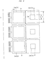
- FIG. 4 is an enlarged partial plan view illustrating an example of a structure of a pad of the main part illustrating the semiconductor device illustrated in FIG. 1
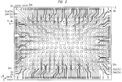
- FIG. 5 is a plan view illustrating each example of a pad array and a rewiring of the main part of the semiconductor device illustrated in FIG. 1 ;
- FIG. 5 is a plan view illustrating each example of a pad array and a rewiring of the main part of the semiconductor device illustrated in FIG. 1 ;
- FIG. 1 is a partial plan view transparently illustrating an example of an internal structure of the main part of the semiconductor device according to an embodiment
- FIG. 6 is an enlarged partial plan view and an enlarged partial cross-sectional view illustrating an example of a structure of a part A of FIG. 5 ; and
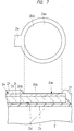
- FIG. 7 is an enlarged partial plan view and an enlarged partial cross-sectional view illustrating an example of a structure of a part B of FIG. 5 .
- a semiconductor device is a wafer process package 5, and a small semiconductor package which is substantially equal to a size of a chip.
- the wafer process package 5 includes a semiconductor chip 2 having a main surface 2b, in which a semiconductor circuit is formed on the main surface 2b, a plurality of first pad electrodes 2aa which are electrically connected to the semiconductor circuit and exposed at the main surface 2b, and a plurality of second pad electrodes 2ab which are electrically connected to each of the plurality of first pad electrodes 2aa, and formed on the same layer with each of the plurality of first pad electrodes 2aa.
- a plurality of pad electrodes 2a are provided side by side in two columns, and there are those which are arranged side by side at the outer side are the plurality of first pad electrodes 2aa while there are those which are arranged side by side at the inner side are the plurality of second pad electrodes 2ab as illustrated in FIG. 1 .
- rearrangement wirings (wirings) 2e are connected to each of the plurality of second pad electrodes 2ab.
- the rearrangement wiring 2e is provided for rearranging each position of the plurality of second pad electrodes 2ab to a different position, and is also called the rewiring.
- each of the plurality of first pad electrodes 2aa is arranged side by side on an end portion side (peripheral edge portion side) of the main surface 2b of the semiconductor chip 2, and each of the plurality of second pad electrodes 2ab is arranged at the inner side than each of the plurality of first pad electrodes 2aa. Further, the rearrangement wiring 2e is led out from each of the plurality of second pad electrodes 2ab arranged at the inner side.
- the rearrangement wiring 2e covers each of the plurality of second pad electrodes 2ab, and further, is electrically connected to each of the plurality of second pad electrodes 2ab as illustrated in FIG. 2 .
- bump lands 2ac are formed at end portions on the opposite side of the second pad electrodes 2ab of the rearrangement wirings 2e, and each of a solder bump (bump) 3 is mounted to each of the bump lands 2ac as an external terminal of the wafer process package 5.
- a polyimide layer 2f serving as an insulating film is formed on each of the plurality of rearrangement wirings 2e, further, the bump land 2ac is formed in an opening portion 2m of the polyimide layer 2f on each of the plurality of rearrangement wirings 2e, and the solder bump 3 is provided on each of the bump lands 2ac.
- each surface of the plurality of first pad electrodes 2aa arranged at the outer side is exposed.
- a first cap film (first metal film) 2r is formed on each surface of the first pad electrodes 2aa, and further, an organic reaction layer 2ka is formed on the first cap film 2r as illustrated in FIG. 2 .
- the first cap film 2r extends on each of the plurality of second pad electrodes 2ab.
- the first cap film 2r is formed on a surface of an Al (aluminum) pad 2s in the first pad electrode 2aa, and further, the organic reaction layer 2ka, which is an organic thin film, is formed on the surface of the first cap film 2r as illustrated in FIG. 2 .
- the Al pad 2s of the first pad electrode 2aa is linked with the Al pad 2s of the second pad electrode 2ab. That is, the Al pad 2s of the first pad electrode 2aa and the Al pad 2s of the second pad electrode 2ab are integrally formed.
- the Al pad 2s according to the present embodiment is considered also as the Al pad 2s equipped with a cap film.
- a second cap film (second metal film) 2t is also formed on a surface of the Al pad 2s in a region of the second pad electrode 2ab. That is, the first cap film 2r and the second cap film 2t are also integrally formed on the Al pad 2s.
- rearrangement wiring 2e is connected to the second pad electrode 2ab.
- the first cap film 2r and the second cap film 2t are made of, for example, TiN (titanium nitride). Accordingly, the first cap film 2r made of TiN is exposed to the first pad electrode 2aa.
- the rearrangement wiring 2e has, for example, a three-layer structure, and includes, for example, a seed layer 2hb made of a Cu (copper) film, a Cu layer 2i, and a Ni (nickel) layer 2n from a lower layer side toward an upper layer side.
- a plurality of wiring layers 2u are formed below the first pad electrodes 2aa, a wiring M of each layer is electrically connected via a plug 2w as illustrated in FIG. 3 .
- memory cells 2v are formed on both sides of the plug 2w serving as a drain at the lowermost layer of the wiring layer 2u.
- the memory cell 2v is, for example, a non-volatile memory (flash memory), and the semiconductor circuit including the non-volatile memory circuit is formed in the semiconductor chip 2 according to the present embodiment.
- FIG. 4 is the plan view of each of the first pad electrode 2aa and the second pad electrode 2ab, and a first opening 2ja, which is an opening portion of the first pad electrode 2aa, has a size far larger than that of a second opening 2 jb which is an opening portion of the second pad electrode 2ab (Y > X).
- the first pad electrode 2aa is a pad for a probe test or wire bonding while the second pad electrode 2ab is a pad for rearrangement wiring connection, which will be described later.
- the semiconductor chip 2 illustrated in FIG. 5 has a structure before attaching the solder bump 3 that is illustrated in FIG. 2 thereto.
- the pad electrodes 2a are provided in two columns on the main surface 2b of the semiconductor chip 2 along the peripheral edge portion thereof. Further, the rearrangement wirings 2e are provided on each of the second pad electrodes 2ab in the column at the inner side among the pad electrodes 2a arranged in two columns, and each of the plurality of rearrangement wirings 2e is led out toward the inside of the main surface 2b. Further, the bump lands 2ac are formed at the respective end portions of the rearrangement wirings 2e.
- the respective bump lands 2ac are provided side by side at an equal pitch both in the X direction and in the Y direction on the main surface 2b. That is, the plurality of bump lands 2ac are provided side by side in a lattice style on the main surface 2b.
- the plurality of solder bumps 3 are also arranged in a lattice style when the solder bumps 3 are mounted to each of the plurality of bump lands 2ac.
- FIG. 6 illustrates the plan view and the cross-sectional view of the first pad electrode 2aa and the second pad electrode 2ab.
- the first pad electrode 2aa and the second pad electrode 2ab according to the present embodiment are configured such that the insulating film is interposed in the Al pad 2s having an elongated rectangular planar shape, and two openings are formed in the insulating film. Accordingly, the integrally formed Al pad 2s is divided into two electrode regions and used with the first pad electrode 2aa and the second pad electrode 2ab.
- the Al pad 2s is formed to be integrally linked from the first pad electrode 2aa over the second pad electrode 2ab, and further, the first cap film 2r and the second cap film 2t, which are integrally formed, are arranged on the Al pad 2s. That is, the Al pad 2s is the Al pad 2s equipped with the cap film.
- the first cap film 2r and the second cap film 2t are made of, for example, TiN (titanium nitride).
- the organic reaction layer 2ka which is extremely thin having a thickness of, for example, about several hundred nm (nano meters), is formed on the surface of the first cap film 2r of the first pad electrode 2aa.
- the plurality of wiring layers 2u are formed below the first pad electrode 2aa, and further, the memory cells 2v are formed at the lowermost layer thereof as illustrated in FIG. 3 , and the memory cell 2v is, for example, the non-volatile memory (flash memory) as described above.
- the bump land 2ac is formed at the end portion of the rearrangement wiring 2e led out from the second pad electrode 2ab as illustrated in FIG. 7 .
- An organic reaction layer 2kb which is an organic thin film, is formed on a surface of the Ni layer 2n at the uppermost layer of the bump land 2ac illustrated in FIG. 2 before mounting the solder bump 3d.
- the organic reaction layer 2kb formed on the surface of the bump land 2ac is removed by, for example, ashing at the time of mounting the solder bump 3 to the bump land 2ac. Accordingly, it is possible to cause the bump land 2ac to be wetted with the solder bump 3, and to cause the solder bump 3 to be favorably connected with the bump land 2ac.
- the first pad electrodes 2aa which are at the outer side (end portion side) among the plurality of pad electrodes 2a arranged in two columns on the peripheral edge portion of the main surface 2b of the semiconductor chip 2, remain without any change, and the second pad electrodes 2ab in the inner-side column are connected with the rearrangement wirings 2e.
- the plurality of first pad electrodes 2aa which are different from the electrode for mounting of the bump, are provided at the peripheral edge portion (end portion) of the main surface 2b so that it is possible to implement the probe test using the first pad electrodes 2aa even after the solder bump are mounted. That is, it is possible to perform the probe test by bringing a probe in contact with the first pad electrode 2aa without bringing the probe in contact with the solder bump 3 even after the wafer process package 5 is assembled.
- the first pad electrode 2aa and the second pad electrode 2ab may be formed by dividedly providing the two openings of the insulating film may be formed at the upper layer of the single elongated Al pad 2s as in the present embodiment, or by forming different Al pads 2s in advance and forming the first pad electrode 2aa and the second pad electrode 2ab to the Al pads 2s, respectively.
- FIGS. 8 to 12 is a flow chart with a cross-sectional view illustrating a part of the method of manufacturing the semiconductor device of FIG. 1 .
- pad opening (leaving a cap) illustrated in FIG. 8 is performed.
- a semiconductor wafer (semiconductor substrate) 1 which includes the plurality of semiconductor chips 2 each of which has a first region 2x and a second region 2y different from the first region 2x formed therein, is prepared.
- the plurality of wiring layers 2u, the first pad electrode 2aa provided with the first cap film 2r formed at the uppermost layer of the plurality of wiring layers 2u in the first region 2x, and the second pad electrode 2ab provided with the second cap film 2t formed at the uppermost layer of the plurality of wiring layers 2u in the second region 2y, which are illustrated in FIG. 3 are formed in each region of the semiconductor chips 2 of the semiconductor wafer 1.
- the Al pad 2s which is formed in an integrally linked manner, is formed with respect to the first pad electrode 2aa and the second pad electrode 2ab.
- the insulating film is interposed in the Al pad 2s having the elongated rectangular planar shape, the two openings are formed in the insulating film, and the integrally formed Al pad 2s is divided into the two electrode regions and used with the first pad electrode 2aa and the second pad electrode 2ab.
- the opening for the first pad electrode 2aa and the opening for the second pad electrode 2ab are formed in a protective film 2z serving as the insulating film and formed on the elongated Al pad 2s such that the first cap film 2r and the second cap film 2t remain.
- the first cap film 2r and the second cap film 2t which are integrally formed, are arranged on the Al pad 2s. That is, the Al pad 2s is the Al pad 2s equipped with the cap film.
- the first cap film 2r and the second cap film 2t are made of, for example, TiN.
- the plurality of wiring layers 2u are formed below the first pad electrode 2aa, and further, the memory cells 2v are formed at the lowermost layer thereof as illustrated in FIG. 3 , and the memory cell 2v is, for example, a non-volatile memory (flash memory).
- flash memory non-volatile memory
- polyimide layer patterning illustrated in FIG. 8 is performed.
- a polyimide layer 2d is formed on the protective film 2z on a main surface 1a of the semiconductor wafer 1, and thereafter, each upper surface of the first pad electrode 2aa and the second pad electrode 2ab is opened by patterning.
- the polyimide layer (first insulating film) 2d which includes the first opening 2ja causing the first cap film 2r to be exposed on the first pad electrode 2aa, and the second opening 2jb causing the second cap film 2t to be exposed on the second pad electrode 2ab, is formed.
- a size of the first opening 2ja when viewed in a plan view is larger than a size of the second opening 2jb when viewed in a plan view as illustrated in FIG. 4 .
- the first pad electrode 2aa is the pad for the probe test or the wire bonding
- the second pad electrode 2ab is the pad for connection of the rearrangement wiring 2e. Accordingly, the relationship is like the first opening 2ja > the second opening 2jb. Incidentally, it is possible to easily change each size of these pads by adjusting each size of the opening portions of the insulating film (polyimide layer 2d) formed on the pads.
- Ashing illustrated in FIG. 8 is performed after the above-described polyimide layer patterning.
- an organic film (the organic reaction layer), formed on the surface of the second cap film 2t of the second pad electrode 2ab, is removed by the ashing.
- Seed layer sputtering illustrated in FIG. 8 is performed after the above-described ashing.
- the seed layer 2hb is formed (deposited) on the polyimide layer 2d, the first pad electrode 2aa, and the second pad electrode 2ab by sputtering. Accordingly, each of the first pad electrode 2aa and the second pad electrode 2ab is electrically connected to the seed layer 2hb.
- a Cr (chromium) film 2ha is formed as a barrier layer (conductive layer), and a Cu film 2hb is formed on the Cr film 2ha as the seed layer.
- the barrier layer (conductive layer) may be the above-described Cr film 2ha or a film made of titanium (TiN), and a film made of a different material from those of the first cap film 2r and the second cap film 2t is used.
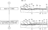
- Resist patterning illustrated in FIG. 9 is performed after the above-described seed layer sputtering.
- the entire region is covered by a resist 2g except for a portion of the rearrangement wiring 2e to be formed in the subsequent step.
- the resist 2g serving as a mask layer that covers the first opening 2ja and causes the second opening 2jb to be exposed is formed on the polyimide layer (first insulating film) 2d with the seed layer 2hb interposed therebetween. That is, an upper surface of the first opening 2ja of the first pad electrode 2aa is covered by the resist 2g, and further the second opening 2jb is exposed without covering an upper surface of the second opening 2jb of the second pad electrode 2ab with the resist 2g.
- Rearrangement wiring-Cu/Ni electroplating formation is performed after the above-described resist patterning.
- the rearrangement wiring (wiring) 2e which is electrically connected to the second pad electrode 2ab and mainly contains Cu, is formed via the second opening 2 jb.
- electroplating formation of Cu is performed, and thereafter, electroplating formation of Ni is performed upon the formation of the rearrangement wiring 2e.
- the Cu layer 2i is formed on the seed layer 2hb inside a region surrounded by the resist (mask layer) 2g by electroplating.
- the rearrangement wiring 2e (the Cu layer 2i) containing Cu as the main component is formed on the seed layer 2hb.
- the Ni layer 2n is formed on the surface of the rearrangement wiring 2e by electroplating.
- the seed layer 2hb, the rearrangement wiring 2e (the Cu layer 2i), and the Ni layer 2n are formed.
- the rearrangement wiring 2e is formed to the second pad electrode 2ab, but is not formed to the first pad electrode 2aa.
- Resist removing and wet etching illustrated in FIG. 10 are performed after the above-described rearrangement wiring-Cu/Ni electroplating formation.
- the resist 2g that surrounds the rearrangement wiring 2e is removed, and further, the seed layer 2hb and the Cr film 2ha on the first pad electrode 2aa (below the resist 2g) are removed.
- the resist 2g serving as the mask layer is removed to expose the first opening 2ja, and further, the Cu film (seed layer) 2hb and the Cr film (conductive layer) on the first cap film 2r are removed by wet etching such that the first cap film 2r of the first pad electrode 2aa remains.
- the barrier layer is the Cr film 2ha
- the first cap film 2r is the TiN film
- the first cap film 2r remains on the Al pad 2s without being removed even when the Cr film 2ha is removed by the wet etching. That is, the Al pad 2s is kept in the state of being covered by the first cap film 2r.
- Polyimide layer patterning illustrated in FIG. 10 is performed after the above-described resist removing and wet etching.
- this polyimide layer patterning first, the polyimide layer (second insulating film) 2f is formed on the rearrangement wiring 2e and on the first pad electrode 2aa. Further, an upper part of the end portion of the rearrangement wiring 2e and the upper surface of the first pad electrode 2aa are opened by patterning.
- a third opening 2ma is formed above the first pad electrode 2aa of the polyimide layer 2f such that the organic reaction layer 2ka remains on the surface of the first pad electrode 2aa
- a fourth opening 2mb is formed at an end portion (bump land 2ac) of the polyimide layer 2f such that the organic reaction layer 2kb remains on the surface of the end portion (bump land 2ac) of the rearrangement wiring 2e. That is, the organic reaction layer 2ka is formed on the surface of the first pad electrode 2aa, and further, the organic reaction layer 2kb is formed on the surface of the bump land 2ac by not performing the ashing.
- each thickness of the organic reaction layer 2ka and the organic reaction layer 2kb, which are formed at this time, is about 100 nm, for example.
- the organic reaction layer 2ka is formed on a surface of the third opening 2ma of the first pad electrode 2aa, and the organic reaction layer 2kb is formed on a surface of the fourth opening 2mb in the bump land 2ac of the end portion of the rearrangement wiring 2e.
- the first cap film 2r on the Al pad 2s is not exposed in the third opening 2ma of the first pad electrode 2aa, nor is the Ni layer 2n of the rearrangement wiring 2e exposed in the fourth opening 2mb of the bump land 2ac of the rearrangement wiring 2e.
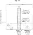
- FIG. 13 is a data diagram illustrating a relation between a thickness of an oxide film and the organic reaction layer in the method of manufacturing the semiconductor device of FIG. 1 , and illustrates a ratio of the oxide film thickness on the basis of an initial stage of the heat processing for a memory test and a stage after the processing, and further, on the basis of "presence” and "absence” of the organic reaction layer.
- the vertical axis in FIG. 13 uses a maximum oxide film thickness (thickness of a Ni oxide film), which enables the Au plating to be formed, as Reference 1, and FIG. 13 illustrates that the Au plating can be formed in a range under or equal to Reference 1.
- a ratio is 0.5 below Reference 1 when the organic reaction layer is present after the heat processing (retention baking) for the memory test, and a ratio becomes 4.0 significantly above Reference 1 when the organic reaction layer is absent. That is, FIG. 13 illustrates that it is possible to form the Au plating even after the heat processing for the memory test as long as the organic reaction layer is formed on a metal surface.
- the Au plating may be formed if the cost is not considered.
- the probe test and programming illustrated in FIG. 11 are performed after the above-described polyimide layer patterning.
- this probe test (first probe test)
- a probe needle 4 is brought into contact with the first pad electrode 2aa to perform an electrical test, and data is programmed in the non-volatile memory (memory cell 2v).
- the organic reaction layer 2ka and the first cap film 2r on the surface of the first pad electrode 2aa are pierced through by the probe needle 4 so that the probe needle 4 is brought into contact with the Al pad 2s, and the probe test (the first probe test and the programming of data in the non-volatile memory) is performed in this state.
- the first pad electrode 2aa which is different from the second pad electrode 2ab, is formed to be exposed to the outside other than the second pad electrode 2ab for the connection of the rearrangement wiring 2e in the assembly of the semiconductor device according to the present embodiment, and thus, it is possible to perform the probe test by bringing the probe needle 4 into contact with the first pad electrode 2aa.
- Baking at 250°C for 12 h illustrated in FIG. 11 is performed after the above-described probe test and programming. That is, heat processing is performed with respect to the semiconductor wafer 1.
- This heat processing is a baking test (thermal load test) of the non-volatile memory (flash memory) formed in the semiconductor chip 2, and is also called a retention baking test, in which, for example, the semiconductor wafer 1 is heated at 250°C for 12 hours (there also is a test performed for 72 hours when the test time is long).
- the temperature of 250°C of the heat processing described above is higher than a melting point of the solder bump 3 (for example, 230°C in the case of a lead-free solder).
- the solder bump 3 is melted when the retention baking test of the non-volatile memory is performed after mounting the solder bump 3, and thus, it is necessary to perform the retention baking test before mounting the solder bump 3.
- the heating is performed at 250°C for a long period of time in the retention baking test, and thus, there is a risk that an oxide film is formed on the surface of the rearrangement wiring 2e of the bump land 2ac, but the oxidation of the Ni layer 2n does not proceed since the organic reaction layer 2kb is formed on the surface of the rearrangement wiring 2e of the bump land 2ac. That is, it is possible to prevent the oxidation of Ni in the bump land 2ac caused by the high-temperature baking (retention baking) (it is possible to protect the Ni layer 2n of the rearrangement wiring 2e using the organic reaction layer 2kb).
- the probe test and a retention test illustrated in FIG. 11 are performed after the above-described baking at 250°C for 12 hours.
- the probe needle 4 is brought into contact with the first pad electrode 2aa to perform a second probe test.
- the above-described second probe test tests after the high-temperature baking of the non-volatile memory (memory cell 2v), whether the programmed data of the memory is lost or whether data failure occurs, for example.
- the first pad electrode 2aa different from the second pad electrode 2ab to which the rearrangement wiring 2e is connected, is formed to be exposed to the outside also in this second probe test.
- Ashing illustrated in FIG. 12 is performed after the above-described probe test and retention test.
- the organic reaction layer 2kb formed on the surface of the rearrangement wiring 2e of the bump land 2ac is removed by the ashing, and accordingly, the Ni layer 2n of the bump land 2ac is exposed.
- the Au plating may be formed on the surface of the bump land 2ac in order to improve the wettability of the solder bump 3.
- Bump formation illustrated in FIG. 12 is performed after the above-described ashing.
- the solder bump 3 is mounted on the bump land 2ac which is exposed through the fourth opening 2mb of the rearrangement wiring 2e.
- the bump is mounted using a flux to activate the Ni layer 2n, and thereafter, reflow is performed to heat the solder bump 3, thereby melting the solder bump 3.
- the solder bump 3 and the Ni layer 2n of the bump land 2ac are connected to each other.
- the bump formation is completed. Accordingly, the Al pad 2s and the solder bump 3 of the semiconductor chip 2 are electrically connected via the rearrangement wiring 2e.
- An appearance and shear test illustrated in FIG. 12 is performed after the above-described bump formation. In this step, an appearance test of the semiconductor wafer 1 is performed, and connection strength of the solder bump 3 is tested using a shear stress.
- the respective semiconductor chips 2 are cut out for singulation by dicing into pieces from the semiconductor wafer 1 after the above-described appearance and shear test, and the assembly of the wafer process package 5 illustrated in FIG. 1 is completed.
- the wafer process package 5 has the structure in which the non-volatile memory is formed in the semiconductor chip 2.
- a memory retention test of the non-volatile memory is sometimes required, but it is not possible to perform the test after mounting the bump since the test is performed at the temperature of 250°C for 8 hours, for example, and such a temperature is higher than 230°C, which is the melting point of the lead-free solder bump.
- a maximum temperature in the rewiring process is 350°C, and thus if any memory loss occurs, that is meaningless. It is necessary to provide the wafer process package that allows the memory to be performed before mounting the bump after forming the rewiring on the basis of such backgrounds.
- the memory test is performed by bringing the probe needle 4 into contact with the pad of the rearrangement wiring 2e in the above-described memory test.
- the accuracy of the test decreases since the Ni layer 2n formed on the surface of the Cu layer 2i of the rearrangement wiring 2e has a large contact resistance.
- it is considered to perform the Au plating on the pad of the rearrangement wiring 2e in order to achieve a countermeasure against the contact resistance of the probe needle 4 and to secure the wettability of the solder bump 3, which causes Ni to spring up and be oxidized on the Au-plated film due to the retention baking, and as a result, leads to an increase of the contact resistance of the probe needle 4 and poor wettability and defective bonding of the solder.
- the Al pad equipped with a metal cap as well as the rewiring structure is newly added to the semiconductor chip 2 which requires to be tested at high temperature that exceeds the melting point of the solder such as the memory retention test for a long period of time.
- each of the first pad electrode 2aa for the test and the second pad electrode 2ab for the lead-out of the rearrangement wiring (rewiring) 2e is provided on the main surface 2b of the semiconductor chip 2.
- the first pad electrode 2aa which is close to the chip end portion as illustrated in FIG. 4 , is provided for the probe test
- the second pad electrode 2ab for the rearrangement wiring 2e is provided at the inner side than the first pad electrode 2aa.
- the first cap film 2r and the second cap film 2t are linked to be integrally formed on the Al pad 2s of each of the first pad electrode 2aa and the second pad electrode 2ab, and the sizes of the respective openings of the electrodes are adjusted for the probe test and for the rearrangement wiring 2e to be different from each other (the size of the opening for the probe test > the size of the opening for the rearrangement wiring 2e).
- the Al pad 2s of the first pad electrode 2aa and the second pad electrode 2ab is covered by a metal cap film (first cap film 2r and the second cap film 2t) .
- the Al pad 2s is protected by the metal cap film (metal film) even when the test such as the retention baking is performed at high temperature for a long period of time.
- the bump land 2ac provided in the rearrangement wiring 2e (rewiring) is covered by the organic reaction layer 2kb which is extremely thin. Accordingly, it is possible to prevent the bump land 2ac from being oxidized or corroded during the heat processing such as the retention baking.
- the thin organic reaction layer 2ka is left on the first cap film 2r of the first pad electrode 2aa provided for the probe test by not performing the ashing to process organic residues after forming the opening in the polyimide layer 2f at the upper layer. As a result, it is possible to protect the Al pad 2s in the process of forming the rearrangement wiring 2e.
- solder bump 3 is mounted to the bump land 2ac of the rearrangement wiring 2e to which the solder bump 3 is mounted after performing the ashing to remove the organic reaction layer 2kb and to expose the Ni layer 2n of the bump land 2ac.
- the bump land 2ac is formed by leading out the rearrangement wiring 2e from the second pad electrode 2ab, it is possible to correspond to a decrease in pitch of the bump land 2ac.
- the first pad electrode 2aa for the test (probe test) and the bump land 2ac for the bump mounting are divided, and thus, the bump mounting is performed after the high-temperature storage test such as the retention baking, the quality of the bump mounting is not degraded. Further, it is possible to perform the test using the first pad electrode 2aa for the test even after mounting the bump in the wafer process package 5 according to the present embodiment.
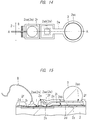
- FIG. 14 is an enlarged partial plan view illustrating a structure of a modification example of the embodiment
- FIG. 15 is a partial cross-sectional view illustrating a structure taken along a line A-A illustrated in FIG. 14
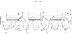
- FIG. 16 is a cross-sectional view illustrating a structure of a semiconductor device to which the modification example of the embodiment is applied.
- the modification example has structure in which the semiconductor chip 2 according to the embodiment described above is incorporated in a system in package (SIP) 6 illustrated in FIG. 16 , and chips are electrically connected to each other using a wire 8.
- SIP system in package
- the semiconductor device has the structure in which the wire (metal wire) 8 is connected to the first pad electrode 2aa for the probe test illustrated in FIG. 14 , and the neighboring semiconductor chips 2 are connected using via wire as illustrated in FIG. 16 .
- the wire 8 such as the metal wire is connected to the first pad electrode 2aa for the test (probe test), which is arranged near an end portion (outer peripheral portion) of the semiconductor chip 2 as illustrated in FIG. 15 .
- the first pad electrode 2aa is used for the pad for the wire bonding, it is possible to apply the semiconductor device to the SIP 6 which is a chip on chip (COC) as illustrated in FIG. 16 .
- COC chip on chip
- the SIP 6 illustrated in FIG. 16 is configured such that small semiconductor chips 7 are mounted on each of the plurality of semiconductor chips 2, which are mounted on a package substrate 9, via the plurality of solder bumps 3 using flip-chip connection.
- the plurality of semiconductor chips 2 are mounted on the package substrate 9 such that the respective back surfaces 2c thereof oppose the package substrate 9 using face-up mounting, and further, the small semiconductor chips 7 are flip-chip connected with each other via the plurality of solder bumps 3 on the semiconductor chip 2, respectively.
- the neighboring semiconductor chips 2 are electrically connected via the wire 8 using a difference in planar size between the semiconductor chip 2 and the semiconductor chip 7. Further, the respective semiconductor chips 2 and the plurality of wires 8 are resin-sealed by a sealing body 11 made of resin. In addition, a plurality of ball electrodes 10 are provided on a lower surface of the package substrate 9 as external terminals. That is, the SIP 6 illustrated in FIG. 16 is the semiconductor device of a type in which the flip-chip mounting and the wire bonding mounting are mixed.
- the semiconductor chip 7 on an upper stage side is, for example, a memory chip
- the semiconductor chip 2 on a lower stage side is, for example, a control chip that controls the semiconductor chip 7.
- the first pad electrode 2aa and the second pad electrode 2ab are formed to the semiconductor chip 2, the first pad electrode 2aa is used for the wire connection, and the second pad electrode 2ab is used for the lead-out of the rearrangement wiring 2e as illustrated in FIGS. 14 and 15 .
- the bump land 2ac formed at the rearrangement wiring 2e is used as the flip-chip connection of the semiconductor chip 7 on the upper stage side, and the semiconductor chip 2 on the lower stage side and the semiconductor chip 7 on the upper stage side are electrically connected via the plurality of solder bumps 3.
- the semiconductor device is the wafer process package in the above-described embodiment, but the above-described semiconductor device may be another semiconductor package as long as including the rearrangement wiring and the semiconductor chip 2 which is provided with the second pad electrode 2ab to which the rearrangement wiring is connected, and the first pad electrode 2aa different from the second pad electrode 2ab.
- first pad electrode 2aa and the second pad electrode 2ab are provided on the single integrally-formed Al pad 2s in the above-described embodiment, but the first pad electrode 2aa and the second pad electrode 2ab may be pads in a structure of being formed on the different Al pads 2s, and are connected via an internal wiring.
Landscapes
- Engineering & Computer Science (AREA)
- Physics & Mathematics (AREA)
- General Physics & Mathematics (AREA)
- Manufacturing & Machinery (AREA)
- Computer Hardware Design (AREA)
- Microelectronics & Electronic Packaging (AREA)
- General Engineering & Computer Science (AREA)
- Geometry (AREA)
- Internal Circuitry In Semiconductor Integrated Circuit Devices (AREA)
Abstract
Description
- The present invention relates to technique of manufacturing a semiconductor device, for example, technique for a wafer process package and so forth, and to a semiconductor device.
- In a wafer process package (WPP, or referred to also as a wafer level package (WLP)), a solder bump is bonded to each terminating end of a plurality of rearrangement wirings (rewirings).
- There is a description in, for example,
Japanese Patent Application Laid-Open No. 2009-246218 Patent Document 1 discloses technique in which a probe needle is brought into contact with an electrode of a wafer process package. - In the above-described wafer process package, there is a step of testing a non-volatile memory during an assembly process when the non-volatile memory is incorporated in a semiconductor chip. This testing step includes a heat processing step, which is called a retention baking step, in which data is programmed in the non-volatile memory, and then, a thermal load is applied at 250°C for about 72 hours, for example. Further, it is checked whether there is a loss in the data programmed in the memory after the retention baking step.
- Here, when the rearrangement wiring is formed after the step of testing the memory, for example, there is a possibility that the data programmed in the memory is lost in the heat processing at high temperature which is implemented at the time of forming the rearrangement wiring. Accordingly, it is preferable to perform the step of testing the non-volatile memory after forming the rearrangement wiring in order to prevent the loss in the data programmed in the memory.
- In this case, the memory test is performed by bringing the probe into contact with a pad of the rearrangement wiring in the above-described step of testing the non-volatile memory, but accuracy of the test decreases since a Ni (nickel) layer formed on a surface of a Cu (copper) layer of the rearrangement wiring is hard and a contact resistance with the probe is large. At this time, it is considered to perform Au plating on the pad of the rearrangement wiring in order to achieve a countermeasure against the contact resistance of the probe and to secure the wettability of the solder bump, which causes Ni to spring up and be oxidized on an Au (gold)-plated film due to the retention baking, and as a result, leads to an increase of the contact resistance of the probe and defective wettability and defective bonding of the solder.
- Other problems and novel features will become apparent from the description of the specification and the attached drawings.
- In a method of manufacturing a semiconductor device of an embodiment of the present invention, a semiconductor substrate is prepared, the semiconductor substrate including a first pad electrode and a second pad electrode, the first pad electrode being formed at an uppermost layer of a plurality of wiring layers and having a first metal film formed on a surface of the first pad electrode, and the second pad electrode being electrically connected to the first pad electrode, being formed at the uppermost layer of the plurality of wiring layers and having a second metal film formed on a surface of the second pad electrode. Further, a first insulating film is formed having a first opening for exposing the first metal film of the first pad electrode, and a second opening for exposing the second metal film in the second pad electrode. A wiring which is electrically connected to the second pad electrode via the second opening is formed. Further, a third opening is formed in a second insulating film above the first pad electrode and a fourth opening of the second insulating film above the wiring is formed while leaving an organic reaction layer on each surface of the first pad electrode and the wiring. Still further, after forming the fourth opening, heat processing is performed on the semiconductor substrate, and then a bump is formed in the fourth opening on the wiring.
- A semiconductor device of an embodiment includes: a semiconductor chip having a main surface in which a semiconductor circuit is formed; a plurality of first pad electrodes electrically connected to the semiconductor circuit and are exposed at the main surface; a plurality of second pad electrodes electrically connected to the plurality of first pad electrodes, respectively, and formed on the same layer with each of the plurality of first pad electrodes; and a plurality of wirings covering each of the plurality of second pad electrodes and are electrically connected to the plurality of second pad electrodes, respectively. Further, the semiconductor device includes an insulating film formed on the plurality of wirings; and a plurality of bumps provided in opening portions of the insulating films of the plurality of wirings. Each surface of the plurality of first pad electrodes is exposed.
- According to the embodiment described above, in a test of a semiconductor device, reliability of the test can be improved with suppressing a defective solder joint.
- In the drawings:
-
FIG. 1 is a partial plan view transparently illustrating an example of an internal structure of the main part of the semiconductor device according to an embodiment; -
FIG. 2 is a cross-sectional view illustrating a structure taken along a line A-A illustrated inFIG. 1 ; -
FIG. 3 is an enlarged partial cross-sectional view illustrating an example of the internal structure of the main part of the semiconductor device illustrated inFIG. 1 ; -
FIG. 4 is an enlarged partial plan view illustrating an example of a structure of a pad of the main part illustrating the semiconductor device illustrated inFIG. 1 ; -
FIG. 5 is a plan view illustrating each example of a pad array and a rewiring of the main part of the semiconductor device illustrated inFIG. 1 ; -
FIG. 6 is an enlarged partial plan view and an enlarged partial cross-sectional view illustrating an example of a structure of a part A ofFIG. 5 ; -
FIG. 7 is an enlarged partial plan view and an enlarged partial cross-sectional view illustrating an example of a structure of a part B ofFIG. 5 ; -
FIG. 8 is a flow chart with a cross-sectional view illustrating a part of a manufacturing method of the semiconductor device ofFIG. 1 ; -
FIG. 9 is a flow chart with a cross-sectional view illustrating a part of the manufacturing method of the semiconductor device ofFIG. 1 ; -
FIG. 10 is a flow chart with a cross-sectional view illustrating a part of the manufacturing method of the semiconductor device ofFIG. 1 ; -
FIG. 11 is a flow chart with a cross-sectional view illustrating a part of the manufacturing method of the semiconductor device ofFIG. 1 ; -
FIG. 12 is a flow chart with a cross-sectional view illustrating a part of the manufacturing method of the semiconductor device ofFIG. 1 ; -
FIG. 13 is a data diagram illustrating a relationship of a thickness of an oxide film and an organic reaction layer in the method of manufacturing the semiconductor device; -
FIG. 14 is an enlarged partial plan view illustrating a structure of a modification example of the embodiment; -
FIG. 15 is a partial cross-sectional view illustrating a structure taken along a line A-A illustrated inFIG. 14 ; and -
FIG. 16 is a cross-sectional view illustrating a structure of a semiconductor device to which the modification example of the embodiment is applied. - In an embodiment described hereinafter, repetitive descriptions of the same or similar components will be omitted.
- In the embodiments described below, the invention will be described in a plurality of sections or embodiments when required as a matter of convenience. However, these sections or embodiments are not irrelevant to each other unless otherwise stated, and the one relates to the entire or a part of the other as a modification example, details, or a supplementary explanation thereof.
- Also, in the embodiments described below, when referring to the number of elements (including number of pieces, values, amount, range, and the like), the number of the elements is not limited to a specific number unless otherwise stated or except the case where the number is apparently limited to a specific number in principle. The number larger or smaller than the specified number is also applicable.
- Further, in the embodiments described below, it goes without saying that the components (including element steps) are not always indispensable unless otherwise stated or except the case where the components are apparently indispensable in principle.
- Further, it is needless to say that such phrases as "formed of A", "made of A", "comprising A", "including A", "having A" do not eliminate other elements than A unless otherwise stated that the element is limited to that. Similarly, in the embodiments described below, when the shape of the components, positional relation thereof, and the like are mentioned, the substantially approximate and similar shapes and the like are included therein unless otherwise stated or except the case where it is conceivable that they are apparently excluded in principle. The same goes for the numerical value and the range described above.
- Hereinafter, the embodiment of the present invention will be described in detail based on the accompanying drawings. Note that, in all of the drawings for describing the embodiments, identical members are provided with the same reference character in principle, and are not repetitively described. Note that even a plan view may be hatched in order to make the drawing easily understood.
-
FIG. 1 is a partial plan view transparently illustrating an example of an internal structure of the main part of the semiconductor device according to an embodiment;FIG. 2 is a cross-sectional view illustrating a structure taken along a line A-A illustrated inFIG. 1 ;FIG. 3 is an enlarged partial cross-sectional view illustrating an example of the internal structure of the main part of the semiconductor device illustrated inFIG. 1 ; andFIG. 4 is an enlarged partial plan view illustrating an example of a structure of a pad of the main part illustrating the semiconductor device illustrated inFIG. 1 . In addition,FIG. 5 is a plan view illustrating each example of a pad array and a rewiring of the main part of the semiconductor device illustrated inFIG. 1 ;FIG. 6 is an enlarged partial plan view and an enlarged partial cross-sectional view illustrating an example of a structure of a part A ofFIG. 5 ; andFIG. 7 is an enlarged partial plan view and an enlarged partial cross-sectional view illustrating an example of a structure of a part B ofFIG. 5 . - A semiconductor device according to the present embodiment illustrated in
FIG. 1 is awafer process package 5, and a small semiconductor package which is substantially equal to a size of a chip. - A description will be given regarding a configuration of the
wafer process package 5 according to the present embodiment with reference toFIGS. 1 and2 . Thewafer process package 5 includes asemiconductor chip 2 having amain surface 2b, in which a semiconductor circuit is formed on themain surface 2b, a plurality of first pad electrodes 2aa which are electrically connected to the semiconductor circuit and exposed at themain surface 2b, and a plurality of second pad electrodes 2ab which are electrically connected to each of the plurality of first pad electrodes 2aa, and formed on the same layer with each of the plurality of first pad electrodes 2aa. - That is, a plurality of
pad electrodes 2a are provided side by side in two columns, and there are those which are arranged side by side at the outer side are the plurality of first pad electrodes 2aa while there are those which are arranged side by side at the inner side are the plurality of second pad electrodes 2ab as illustrated inFIG. 1 . - Further, rearrangement wirings (wirings) 2e are connected to each of the plurality of second pad electrodes 2ab. The
rearrangement wiring 2e is provided for rearranging each position of the plurality of second pad electrodes 2ab to a different position, and is also called the rewiring. - In other words, each of the plurality of first pad electrodes 2aa is arranged side by side on an end portion side (peripheral edge portion side) of the
main surface 2b of thesemiconductor chip 2, and each of the plurality of second pad electrodes 2ab is arranged at the inner side than each of the plurality of first pad electrodes 2aa. Further, therearrangement wiring 2e is led out from each of the plurality of second pad electrodes 2ab arranged at the inner side. - Specifically, the
rearrangement wiring 2e covers each of the plurality of second pad electrodes 2ab, and further, is electrically connected to each of the plurality of second pad electrodes 2ab as illustrated inFIG. 2 . Further, bump lands 2ac are formed at end portions on the opposite side of the second pad electrodes 2ab of therearrangement wirings 2e, and each of a solder bump (bump) 3 is mounted to each of the bump lands 2ac as an external terminal of thewafer process package 5. - Specifically, a
polyimide layer 2f serving as an insulating film is formed on each of the plurality ofrearrangement wirings 2e, further, the bump land 2ac is formed in anopening portion 2m of thepolyimide layer 2f on each of the plurality ofrearrangement wirings 2e, and thesolder bump 3 is provided on each of the bump lands 2ac. - Incidentally, each surface of the plurality of first pad electrodes 2aa arranged at the outer side is exposed. Specifically, a first cap film (first metal film) 2r is formed on each surface of the first pad electrodes 2aa, and further, an organic reaction layer 2ka is formed on the
first cap film 2r as illustrated inFIG. 2 . In addition, thefirst cap film 2r extends on each of the plurality of second pad electrodes 2ab. - Specifically, the
first cap film 2r is formed on a surface of an Al (aluminum)pad 2s in the first pad electrode 2aa, and further, the organic reaction layer 2ka, which is an organic thin film, is formed on the surface of thefirst cap film 2r as illustrated inFIG. 2 . Further, theAl pad 2s of the first pad electrode 2aa is linked with theAl pad 2s of the second pad electrode 2ab. That is, theAl pad 2s of the first pad electrode 2aa and theAl pad 2s of the second pad electrode 2ab are integrally formed. In other words, theAl pad 2s according to the present embodiment is considered also as theAl pad 2s equipped with a cap film. - Further, a second cap film (second metal film) 2t is also formed on a surface of the
Al pad 2s in a region of the second pad electrode 2ab. That is, thefirst cap film 2r and thesecond cap film 2t are also integrally formed on theAl pad 2s. - Further, the
rearrangement wiring 2e is connected to the second pad electrode 2ab. - Incidentally, the
first cap film 2r and thesecond cap film 2t are made of, for example, TiN (titanium nitride). Accordingly, thefirst cap film 2r made of TiN is exposed to the first pad electrode 2aa. - In addition, the
rearrangement wiring 2e has, for example, a three-layer structure, and includes, for example, a seed layer 2hb made of a Cu (copper) film, aCu layer 2i, and a Ni (nickel)layer 2n from a lower layer side toward an upper layer side. - In addition, a plurality of
wiring layers 2u are formed below the first pad electrodes 2aa, a wiring M of each layer is electrically connected via aplug 2w as illustrated inFIG. 3 . Further,memory cells 2v are formed on both sides of theplug 2w serving as a drain at the lowermost layer of thewiring layer 2u. Thememory cell 2v is, for example, a non-volatile memory (flash memory), and the semiconductor circuit including the non-volatile memory circuit is formed in thesemiconductor chip 2 according to the present embodiment. - In addition,
FIG. 4 is the plan view of each of the first pad electrode 2aa and the second pad electrode 2ab, and a first opening 2ja, which is an opening portion of the first pad electrode 2aa, has a size far larger than that of asecond opening 2 jb which is an opening portion of the second pad electrode 2ab (Y > X). This is because the first pad electrode 2aa is a pad for a probe test or wire bonding while the second pad electrode 2ab is a pad for rearrangement wiring connection, which will be described later. - It is possible to easily change each size of these pads by adjusting a size of an opening portion of an insulating film formed in the pad.
- Next, a description will be given regarding a structure of the pad of the semiconductor chip to be mounted to the
wafer process package 5 according to the present embodiment. - The
semiconductor chip 2 illustrated inFIG. 5 has a structure before attaching thesolder bump 3 that is illustrated inFIG. 2 thereto. - The
pad electrodes 2a are provided in two columns on themain surface 2b of thesemiconductor chip 2 along the peripheral edge portion thereof. Further, therearrangement wirings 2e are provided on each of the second pad electrodes 2ab in the column at the inner side among thepad electrodes 2a arranged in two columns, and each of the plurality ofrearrangement wirings 2e is led out toward the inside of themain surface 2b. Further, the bump lands 2ac are formed at the respective end portions of therearrangement wirings 2e. - Incidentally, the respective bump lands 2ac are provided side by side at an equal pitch both in the X direction and in the Y direction on the
main surface 2b. That is, the plurality of bump lands 2ac are provided side by side in a lattice style on themain surface 2b. - Accordingly, the plurality of
solder bumps 3 are also arranged in a lattice style when the solder bumps 3 are mounted to each of the plurality of bump lands 2ac. -
FIG. 6 illustrates the plan view and the cross-sectional view of the first pad electrode 2aa and the second pad electrode 2ab. The first pad electrode 2aa and the second pad electrode 2ab according to the present embodiment are configured such that the insulating film is interposed in theAl pad 2s having an elongated rectangular planar shape, and two openings are formed in the insulating film. Accordingly, the integrally formedAl pad 2s is divided into two electrode regions and used with the first pad electrode 2aa and the second pad electrode 2ab. - Accordingly, the
Al pad 2s is formed to be integrally linked from the first pad electrode 2aa over the second pad electrode 2ab, and further, thefirst cap film 2r and thesecond cap film 2t, which are integrally formed, are arranged on theAl pad 2s. That is, theAl pad 2s is theAl pad 2s equipped with the cap film. Incidentally, thefirst cap film 2r and thesecond cap film 2t are made of, for example, TiN (titanium nitride). - Further, the organic reaction layer 2ka, which is extremely thin having a thickness of, for example, about several hundred nm (nano meters), is formed on the surface of the
first cap film 2r of the first pad electrode 2aa. - In addition, the plurality of
wiring layers 2u are formed below the first pad electrode 2aa, and further, thememory cells 2v are formed at the lowermost layer thereof as illustrated inFIG. 3 , and thememory cell 2v is, for example, the non-volatile memory (flash memory) as described above. - In addition, the bump land 2ac is formed at the end portion of the
rearrangement wiring 2e led out from the second pad electrode 2ab as illustrated inFIG. 7 . An organic reaction layer 2kb, which is an organic thin film, is formed on a surface of theNi layer 2n at the uppermost layer of the bump land 2ac illustrated inFIG. 2 before mounting the solder bump 3d. - Incidentally, the organic reaction layer 2kb formed on the surface of the bump land 2ac is removed by, for example, ashing at the time of mounting the
solder bump 3 to the bump land 2ac. Accordingly, it is possible to cause the bump land 2ac to be wetted with thesolder bump 3, and to cause thesolder bump 3 to be favorably connected with the bump land 2ac. - In the
wafer process package 5 according to the present embodiment, the first pad electrodes 2aa, which are at the outer side (end portion side) among the plurality ofpad electrodes 2a arranged in two columns on the peripheral edge portion of themain surface 2b of thesemiconductor chip 2, remain without any change, and the second pad electrodes 2ab in the inner-side column are connected with therearrangement wirings 2e. - Accordingly, the plurality of first pad electrodes 2aa, which are different from the electrode for mounting of the bump, are provided at the peripheral edge portion (end portion) of the
main surface 2b so that it is possible to implement the probe test using the first pad electrodes 2aa even after the solder bump are mounted. That is, it is possible to perform the probe test by bringing a probe in contact with the first pad electrode 2aa without bringing the probe in contact with thesolder bump 3 even after thewafer process package 5 is assembled. - Incidentally, the first pad electrode 2aa and the second pad electrode 2ab may be formed by dividedly providing the two openings of the insulating film may be formed at the upper layer of the single elongated
Al pad 2s as in the present embodiment, or by formingdifferent Al pads 2s in advance and forming the first pad electrode 2aa and the second pad electrode 2ab to theAl pads 2s, respectively. - Next, a description will be given regarding a method of manufacturing the semiconductor device according to the present embodiment. Each of
FIGS. 8 to 12 is a flow chart with a cross-sectional view illustrating a part of the method of manufacturing the semiconductor device ofFIG. 1 . - First, pad opening (leaving a cap) illustrated in
FIG. 8 is performed. In the above-described pad opening, a semiconductor wafer (semiconductor substrate) 1, which includes the plurality ofsemiconductor chips 2 each of which has afirst region 2x and asecond region 2y different from thefirst region 2x formed therein, is prepared. Incidentally, the plurality ofwiring layers 2u, the first pad electrode 2aa provided with thefirst cap film 2r formed at the uppermost layer of the plurality ofwiring layers 2u in thefirst region 2x, and the second pad electrode 2ab provided with thesecond cap film 2t formed at the uppermost layer of the plurality ofwiring layers 2u in thesecond region 2y, which are illustrated inFIG. 3 , are formed in each region of thesemiconductor chips 2 of thesemiconductor wafer 1. - Further, the
Al pad 2s, which is formed in an integrally linked manner, is formed with respect to the first pad electrode 2aa and the second pad electrode 2ab. Specifically, the insulating film is interposed in theAl pad 2s having the elongated rectangular planar shape, the two openings are formed in the insulating film, and the integrally formedAl pad 2s is divided into the two electrode regions and used with the first pad electrode 2aa and the second pad electrode 2ab. - That is, the opening for the first pad electrode 2aa and the opening for the second pad electrode 2ab are formed in a
protective film 2z serving as the insulating film and formed on theelongated Al pad 2s such that thefirst cap film 2r and thesecond cap film 2t remain. Incidentally, thefirst cap film 2r and thesecond cap film 2t, which are integrally formed, are arranged on theAl pad 2s. That is, theAl pad 2s is theAl pad 2s equipped with the cap film. Here, thefirst cap film 2r and thesecond cap film 2t are made of, for example, TiN. - In addition, the plurality of
wiring layers 2u are formed below the first pad electrode 2aa, and further, thememory cells 2v are formed at the lowermost layer thereof as illustrated inFIG. 3 , and thememory cell 2v is, for example, a non-volatile memory (flash memory). - Next, polyimide layer patterning illustrated in
FIG. 8 is performed. In this polyimide layer patterning, apolyimide layer 2d is formed on theprotective film 2z on amain surface 1a of thesemiconductor wafer 1, and thereafter, each upper surface of the first pad electrode 2aa and the second pad electrode 2ab is opened by patterning. In other words, the polyimide layer (first insulating film) 2d, which includes the first opening 2ja causing thefirst cap film 2r to be exposed on the first pad electrode 2aa, and the second opening 2jb causing thesecond cap film 2t to be exposed on the second pad electrode 2ab, is formed. - At this time, a size of the first opening 2ja when viewed in a plan view is larger than a size of the second opening 2jb when viewed in a plan view as illustrated in
FIG. 4 . That is, the first pad electrode 2aa is the pad for the probe test or the wire bonding, and the second pad electrode 2ab is the pad for connection of therearrangement wiring 2e. Accordingly, the relationship is like the first opening 2ja > the second opening 2jb. Incidentally, it is possible to easily change each size of these pads by adjusting each size of the opening portions of the insulating film (polyimide layer 2d) formed on the pads. - Ashing illustrated in
FIG. 8 is performed after the above-described polyimide layer patterning. In the above-described ashing, an organic film (the organic reaction layer), formed on the surface of thesecond cap film 2t of the second pad electrode 2ab, is removed by the ashing. - Seed layer sputtering illustrated in
FIG. 8 is performed after the above-described ashing. In this seed layer sputtering, the seed layer 2hb is formed (deposited) on thepolyimide layer 2d, the first pad electrode 2aa, and the second pad electrode 2ab by sputtering. Accordingly, each of the first pad electrode 2aa and the second pad electrode 2ab is electrically connected to the seed layer 2hb. First, a Cr (chromium) film 2ha is formed as a barrier layer (conductive layer), and a Cu film 2hb is formed on the Cr film 2ha as the seed layer. In addition, the barrier layer (conductive layer) may be the above-described Cr film 2ha or a film made of titanium (TiN), and a film made of a different material from those of thefirst cap film 2r and thesecond cap film 2t is used. - Resist patterning illustrated in
FIG. 9 is performed after the above-described seed layer sputtering. In this resist patterning, the entire region is covered by a resist 2g except for a portion of therearrangement wiring 2e to be formed in the subsequent step. Specifically, the resist 2g serving as a mask layer that covers the first opening 2ja and causes the second opening 2jb to be exposed is formed on the polyimide layer (first insulating film) 2d with the seed layer 2hb interposed therebetween. That is, an upper surface of the first opening 2ja of the first pad electrode 2aa is covered by the resist 2g, and further the second opening 2jb is exposed without covering an upper surface of the second opening 2jb of the second pad electrode 2ab with the resist 2g. - Rearrangement wiring-Cu/Ni electroplating formation, illustrated in
FIG. 9 , is performed after the above-described resist patterning. In this rearrangement wiring-Cu/Ni electroplating formation, the rearrangement wiring (wiring) 2e, which is electrically connected to the second pad electrode 2ab and mainly contains Cu, is formed via thesecond opening 2 jb. First, electroplating formation of Cu is performed, and thereafter, electroplating formation of Ni is performed upon the formation of therearrangement wiring 2e. - Specifically, first, the
Cu layer 2i is formed on the seed layer 2hb inside a region surrounded by the resist (mask layer) 2g by electroplating. In this manner, therearrangement wiring 2e (theCu layer 2i) containing Cu as the main component is formed on the seed layer 2hb. Thereafter, theNi layer 2n is formed on the surface of therearrangement wiring 2e by electroplating. In this manner, the seed layer 2hb, therearrangement wiring 2e (theCu layer 2i), and theNi layer 2n are formed. - As a result, the
rearrangement wiring 2e is formed to the second pad electrode 2ab, but is not formed to the first pad electrode 2aa. - Resist removing and wet etching illustrated in
FIG. 10 are performed after the above-described rearrangement wiring-Cu/Ni electroplating formation. In this resist removing and wet etching, the resist 2g that surrounds therearrangement wiring 2e is removed, and further, the seed layer 2hb and the Cr film 2ha on the first pad electrode 2aa (below the resist 2g) are removed. - That is, the resist 2g serving as the mask layer is removed to expose the first opening 2ja, and further, the Cu film (seed layer) 2hb and the Cr film (conductive layer) on the
first cap film 2r are removed by wet etching such that thefirst cap film 2r of the first pad electrode 2aa remains. - At this time, the barrier layer is the Cr film 2ha, and the
first cap film 2r is the TiN film, and thus, thefirst cap film 2r remains on theAl pad 2s without being removed even when the Cr film 2ha is removed by the wet etching. That is, theAl pad 2s is kept in the state of being covered by thefirst cap film 2r. - Accordingly, it is possible to prevent the
Al pad 2s from corrosion. - Polyimide layer patterning illustrated in
FIG. 10 is performed after the above-described resist removing and wet etching. In this polyimide layer patterning, first, the polyimide layer (second insulating film) 2f is formed on therearrangement wiring 2e and on the first pad electrode 2aa. Further, an upper part of the end portion of therearrangement wiring 2e and the upper surface of the first pad electrode 2aa are opened by patterning. - Specifically, a third opening 2ma is formed above the first pad electrode 2aa of the
polyimide layer 2f such that the organic reaction layer 2ka remains on the surface of the first pad electrode 2aa, and a fourth opening 2mb is formed at an end portion (bump land 2ac) of thepolyimide layer 2f such that the organic reaction layer 2kb remains on the surface of the end portion (bump land 2ac) of therearrangement wiring 2e. That is, the organic reaction layer 2ka is formed on the surface of the first pad electrode 2aa, and further, the organic reaction layer 2kb is formed on the surface of the bump land 2ac by not performing the ashing. Incidentally, it is possible to form the organic reaction layers 2ka and 2kb having the anticorrosive effect in the case of only opening the polyimide layer. Accordingly, theNi layer 2n of the bump land 2ac is not substantially oxidized, and this effect is maintained as long as the ashing is not performed. Each thickness of the organic reaction layer 2ka and the organic reaction layer 2kb, which are formed at this time, is about 100 nm, for example. - In the above-described manner, the organic reaction layer 2ka is formed on a surface of the third opening 2ma of the first pad electrode 2aa, and the organic reaction layer 2kb is formed on a surface of the fourth opening 2mb in the bump land 2ac of the end portion of the
rearrangement wiring 2e. - Accordingly, the
first cap film 2r on theAl pad 2s is not exposed in the third opening 2ma of the first pad electrode 2aa, nor is theNi layer 2n of therearrangement wiring 2e exposed in the fourth opening 2mb of the bump land 2ac of therearrangement wiring 2e. - Further, it is possible to prevent the surface of the bump land 2ac from oxidation using the organic reaction layer 2kb in the present embodiment, and thus, Au (gold) plating formation (immersion gold) is not performed on the surface of the bump land 2ac.
- Here, a description will be given regarding whether the plated film is formed depending on presence or absence of the organic reaction layer with reference to
FIG. 13. FIG. 13 is a data diagram illustrating a relation between a thickness of an oxide film and the organic reaction layer in the method of manufacturing the semiconductor device ofFIG. 1 , and illustrates a ratio of the oxide film thickness on the basis of an initial stage of the heat processing for a memory test and a stage after the processing, and further, on the basis of "presence" and "absence" of the organic reaction layer. Incidentally, the vertical axis inFIG. 13 uses a maximum oxide film thickness (thickness of a Ni oxide film), which enables the Au plating to be formed, asReference 1, andFIG. 13 illustrates that the Au plating can be formed in a range under or equal toReference 1. - According to the oxide film thickness ratios of
FIG. 13 , a ratio is 0.5 belowReference 1 when the organic reaction layer is present after the heat processing (retention baking) for the memory test, and a ratio becomes 4.0 significantly aboveReference 1 when the organic reaction layer is absent. That is,FIG. 13 illustrates that it is possible to form the Au plating even after the heat processing for the memory test as long as the organic reaction layer is formed on a metal surface. - Although the description is given regarding a case in which the Au plating is not performed on the surface of the bump land 2ac in the present embodiment as described above, the Au plating may be formed if the cost is not considered.
- The probe test and programming illustrated in
FIG. 11 are performed after the above-described polyimide layer patterning. In this probe test (first probe test), aprobe needle 4 is brought into contact with the first pad electrode 2aa to perform an electrical test, and data is programmed in the non-volatile memory (memory cell 2v). Specifically, the organic reaction layer 2ka and thefirst cap film 2r on the surface of the first pad electrode 2aa are pierced through by theprobe needle 4 so that theprobe needle 4 is brought into contact with theAl pad 2s, and the probe test (the first probe test and the programming of data in the non-volatile memory) is performed in this state. - In this manner, the first pad electrode 2aa, which is different from the second pad electrode 2ab, is formed to be exposed to the outside other than the second pad electrode 2ab for the connection of the
rearrangement wiring 2e in the assembly of the semiconductor device according to the present embodiment, and thus, it is possible to perform the probe test by bringing theprobe needle 4 into contact with the first pad electrode 2aa. - Baking at 250°C for 12 h illustrated in
FIG. 11 is performed after the above-described probe test and programming. That is, heat processing is performed with respect to thesemiconductor wafer 1. This heat processing is a baking test (thermal load test) of the non-volatile memory (flash memory) formed in thesemiconductor chip 2, and is also called a retention baking test, in which, for example, thesemiconductor wafer 1 is heated at 250°C for 12 hours (there also is a test performed for 72 hours when the test time is long). In this case, the temperature of 250°C of the heat processing described above is higher than a melting point of the solder bump 3 (for example, 230°C in the case of a lead-free solder). - Accordingly, the
solder bump 3 is melted when the retention baking test of the non-volatile memory is performed after mounting thesolder bump 3, and thus, it is necessary to perform the retention baking test before mounting thesolder bump 3. - In addition, the heating is performed at 250°C for a long period of time in the retention baking test, and thus, there is a risk that an oxide film is formed on the surface of the
rearrangement wiring 2e of the bump land 2ac, but the oxidation of theNi layer 2n does not proceed since the organic reaction layer 2kb is formed on the surface of therearrangement wiring 2e of the bump land 2ac. That is, it is possible to prevent the oxidation of Ni in the bump land 2ac caused by the high-temperature baking (retention baking) (it is possible to protect theNi layer 2n of therearrangement wiring 2e using the organic reaction layer 2kb). - The probe test and a retention test illustrated in
FIG. 11 are performed after the above-described baking at 250°C for 12 hours. In this probe test, theprobe needle 4 is brought into contact with the first pad electrode 2aa to perform a second probe test. The above-described second probe test tests, after the high-temperature baking of the non-volatile memory (memory cell 2v), whether the programmed data of the memory is lost or whether data failure occurs, for example. - Incidentally, the first pad electrode 2aa, different from the second pad electrode 2ab to which the
rearrangement wiring 2e is connected, is formed to be exposed to the outside also in this second probe test. Thus, it is possible to perform the second probe test by bringing theprobe needle 4 into contact with the first pad electrode 2aa, similarly to the first probe test. - Ashing illustrated in
FIG. 12 is performed after the above-described probe test and retention test. In this step, the organic reaction layer 2kb formed on the surface of therearrangement wiring 2e of the bump land 2ac is removed by the ashing, and accordingly, theNi layer 2n of the bump land 2ac is exposed. Incidentally, the Au plating may be formed on the surface of the bump land 2ac in order to improve the wettability of thesolder bump 3. - Bump formation illustrated in
FIG. 12 is performed after the above-described ashing. In this bump formation, thesolder bump 3 is mounted on the bump land 2ac which is exposed through the fourth opening 2mb of therearrangement wiring 2e. At this time, the bump is mounted using a flux to activate theNi layer 2n, and thereafter, reflow is performed to heat thesolder bump 3, thereby melting thesolder bump 3. As a result, thesolder bump 3 and theNi layer 2n of the bump land 2ac are connected to each other. - In the above-described manner, the bump formation is completed. Accordingly, the
Al pad 2s and thesolder bump 3 of thesemiconductor chip 2 are electrically connected via therearrangement wiring 2e. - An appearance and shear test illustrated in
FIG. 12 is performed after the above-described bump formation. In this step, an appearance test of thesemiconductor wafer 1 is performed, and connection strength of thesolder bump 3 is tested using a shear stress. - The
respective semiconductor chips 2 are cut out for singulation by dicing into pieces from thesemiconductor wafer 1 after the above-described appearance and shear test, and the assembly of thewafer process package 5 illustrated inFIG. 1 is completed. - Here, the
wafer process package 5 according to the present embodiment has the structure in which the non-volatile memory is formed in thesemiconductor chip 2. In the probe test of the semiconductor substrate in which the non-volatile memory is formed in the above-described manner, a memory retention test of the non-volatile memory is sometimes required, but it is not possible to perform the test after mounting the bump since the test is performed at the temperature of 250°C for 8 hours, for example, and such a temperature is higher than 230°C, which is the melting point of the lead-free solder bump. In addition, even when the test is performed before forming the rewiring, a maximum temperature in the rewiring process is 350°C, and thus if any memory loss occurs, that is meaningless. It is necessary to provide the wafer process package that allows the memory to be performed before mounting the bump after forming the rewiring on the basis of such backgrounds. - Further, the memory test is performed by bringing the
probe needle 4 into contact with the pad of therearrangement wiring 2e in the above-described memory test. The accuracy of the test decreases since theNi layer 2n formed on the surface of theCu layer 2i of therearrangement wiring 2e has a large contact resistance. At this time, it is considered to perform the Au plating on the pad of therearrangement wiring 2e in order to achieve a countermeasure against the contact resistance of theprobe needle 4 and to secure the wettability of thesolder bump 3, which causes Ni to spring up and be oxidized on the Au-plated film due to the retention baking, and as a result, leads to an increase of the contact resistance of theprobe needle 4 and poor wettability and defective bonding of the solder. - In addition, it is also considered to perform the Au plating formation on the pad of the
rearrangement wiring 2e again after the retention baking as a countermeasure against the spring-up of Ni on the Au plated film, but in this case, cost increases because the Au plating is formed twice. - Thus, in the method of manufacturing the semiconductor device according to the present embodiment, the Al pad equipped with a metal cap as well as the rewiring structure is newly added to the
semiconductor chip 2 which requires to be tested at high temperature that exceeds the melting point of the solder such as the memory retention test for a long period of time. Specifically, each of the first pad electrode 2aa for the test and the second pad electrode 2ab for the lead-out of the rearrangement wiring (rewiring) 2e is provided on themain surface 2b of thesemiconductor chip 2. For example, the first pad electrode 2aa, which is close to the chip end portion as illustrated inFIG. 4 , is provided for the probe test, and the second pad electrode 2ab for therearrangement wiring 2e is provided at the inner side than the first pad electrode 2aa. - At this time, the
first cap film 2r and thesecond cap film 2t are linked to be integrally formed on theAl pad 2s of each of the first pad electrode 2aa and the second pad electrode 2ab, and the sizes of the respective openings of the electrodes are adjusted for the probe test and for therearrangement wiring 2e to be different from each other (the size of the opening for the probe test > the size of the opening for therearrangement wiring 2e). In addition, theAl pad 2s of the first pad electrode 2aa and the second pad electrode 2ab is covered by a metal cap film (first cap film 2r and thesecond cap film 2t) . Thus, theAl pad 2s is protected by the metal cap film (metal film) even when the test such as the retention baking is performed at high temperature for a long period of time. - Meanwhile, the bump land 2ac provided in the
rearrangement wiring 2e (rewiring) is covered by the organic reaction layer 2kb which is extremely thin. Accordingly, it is possible to prevent the bump land 2ac from being oxidized or corroded during the heat processing such as the retention baking. - Incidentally, the thin organic reaction layer 2ka is left on the
first cap film 2r of the first pad electrode 2aa provided for the probe test by not performing the ashing to process organic residues after forming the opening in thepolyimide layer 2f at the upper layer. As a result, it is possible to protect theAl pad 2s in the process of forming therearrangement wiring 2e. - As described above, it is possible to obtain both a desired heat resistance and the wettability and bonding property of the solder, and to perform the memory retention test at the high temperature exceeding the melting point of the
solder bump 3 for the long period of time before forming the bump, according to the process and the structure of the present embodiment. - Incidentally, since it is unnecessary to perform the Au plating on the bump land 2ac in the method of manufacturing the semiconductor device according to the present embodiment, it is possible to suppress the cost increase in the test. Accordingly, it is possible to achieve the stabilization of the test and to enhance the reliability of the test while suppressing the cost increase and the defective bonding of the solder in the test of the semiconductor device (semiconductor chip 2).
- In addition, when the test such as the retention baking is performed using the first pad electrode 2aa provided at the end portion of the
main surface 2b of thesemiconductor chip 2, a cantilever is used, and thus, theprobe needle 4 is brought into contact by penetrating the thin organic reaction layer 2ka and thefirst cap film 2r. Accordingly, failure of conduction in the test is not caused. - In addition, the
solder bump 3 is mounted to the bump land 2ac of therearrangement wiring 2e to which thesolder bump 3 is mounted after performing the ashing to remove the organic reaction layer 2kb and to expose theNi layer 2n of the bump land 2ac. Thus, it is possible to mount the bump without inhibiting the alloying reaction with respect to thesolder bump 3. - In addition, since the bump land 2ac is formed by leading out the
rearrangement wiring 2e from the second pad electrode 2ab, it is possible to correspond to a decrease in pitch of the bump land 2ac. - In addition, the first pad electrode 2aa for the test (probe test) and the bump land 2ac for the bump mounting are divided, and thus, the bump mounting is performed after the high-temperature storage test such as the retention baking, the quality of the bump mounting is not degraded. Further, it is possible to perform the test using the first pad electrode 2aa for the test even after mounting the bump in the
wafer process package 5 according to the present embodiment. -
FIG. 14 is an enlarged partial plan view illustrating a structure of a modification example of the embodiment,FIG. 15 is a partial cross-sectional view illustrating a structure taken along a line A-A illustrated inFIG. 14 , andFIG. 16 is a cross-sectional view illustrating a structure of a semiconductor device to which the modification example of the embodiment is applied. - The modification example has structure in which the
semiconductor chip 2 according to the embodiment described above is incorporated in a system in package (SIP) 6 illustrated inFIG. 16 , and chips are electrically connected to each other using awire 8. - That is, the semiconductor device has the structure in which the wire (metal wire) 8 is connected to the first pad electrode 2aa for the probe test illustrated in
FIG. 14 , and the neighboringsemiconductor chips 2 are connected using via wire as illustrated inFIG. 16 . - That is, the
wire 8 such as the metal wire is connected to the first pad electrode 2aa for the test (probe test), which is arranged near an end portion (outer peripheral portion) of thesemiconductor chip 2 as illustrated inFIG. 15 . When the first pad electrode 2aa is used for the pad for the wire bonding, it is possible to apply the semiconductor device to the SIP 6 which is a chip on chip (COC) as illustrated inFIG. 16 . - The SIP 6 illustrated in
FIG. 16 is configured such thatsmall semiconductor chips 7 are mounted on each of the plurality ofsemiconductor chips 2, which are mounted on a package substrate 9, via the plurality ofsolder bumps 3 using flip-chip connection. Specifically, the plurality ofsemiconductor chips 2 are mounted on the package substrate 9 such that the respective back surfaces 2c thereof oppose the package substrate 9 using face-up mounting, and further, thesmall semiconductor chips 7 are flip-chip connected with each other via the plurality ofsolder bumps 3 on thesemiconductor chip 2, respectively. - Further, the neighboring
semiconductor chips 2 are electrically connected via thewire 8 using a difference in planar size between thesemiconductor chip 2 and thesemiconductor chip 7. Further, therespective semiconductor chips 2 and the plurality ofwires 8 are resin-sealed by a sealing body 11 made of resin. In addition, a plurality ofball electrodes 10 are provided on a lower surface of the package substrate 9 as external terminals. That is, the SIP 6 illustrated inFIG. 16 is the semiconductor device of a type in which the flip-chip mounting and the wire bonding mounting are mixed. - In the SIP 6, the
semiconductor chip 7 on an upper stage side is, for example, a memory chip, and thesemiconductor chip 2 on a lower stage side is, for example, a control chip that controls thesemiconductor chip 7. - In the above-described SIP 6, the first pad electrode 2aa and the second pad electrode 2ab are formed to the
semiconductor chip 2, the first pad electrode 2aa is used for the wire connection, and the second pad electrode 2ab is used for the lead-out of therearrangement wiring 2e as illustrated inFIGS. 14 and 15 . Further, the bump land 2ac formed at therearrangement wiring 2e is used as the flip-chip connection of thesemiconductor chip 7 on the upper stage side, and thesemiconductor chip 2 on the lower stage side and thesemiconductor chip 7 on the upper stage side are electrically connected via the plurality of solder bumps 3. - It is possible to apply the
semiconductor chip 2 according to the present embodiment to the COC structure and the SIP structure by forming the first pad electrode 2aa and the second pad electrode 2ab in thesemiconductor chip 2 as described above. - In the foregoing, the invention made by the inventor has been specifically described based on the embodiments. However, it is needless to say that the present invention is not limited to the foregoing embodiments and various modifications can be made within the gist of the present invention.
- The description has been given regarding a case in which the semiconductor device is the wafer process package in the above-described embodiment, but the above-described semiconductor device may be another semiconductor package as long as including the rearrangement wiring and the
semiconductor chip 2 which is provided with the second pad electrode 2ab to which the rearrangement wiring is connected, and the first pad electrode 2aa different from the second pad electrode 2ab. - In addition, the description has been given regarding a case in which the first pad electrode 2aa and the second pad electrode 2ab are provided on the single integrally-formed
Al pad 2s in the above-described embodiment, but the first pad electrode 2aa and the second pad electrode 2ab may be pads in a structure of being formed on thedifferent Al pads 2s, and are connected via an internal wiring. - Further, within the gist of the technical idea described above in the embodiment, one or more combination modification examples can be used.
Claims (14)
- A method of manufacturing a semiconductor device comprising the steps of:(a) preparing a semiconductor substrate that includes a first pad electrode and a second pad electrode, the first pad electrode being formed at an uppermost layer of a plurality of wiring layers and having a first metal film formed on a surface of the first pad electrode, and the second pad electrode being electrically connected to the first pad electrode, being formed at the uppermost layer of the plurality of wiring layers and having a second metal film formed on a surface of the second pad electrode;(b) forming a first insulating film having a first opening, for exposing the first metal film in the first pad electrode, and a second opening for exposing the second metal film in the second pad electrode;(c) forming a mask layer on the first insulating film for covering the first opening and exposing the second opening;(d) forming a wiring which is electrically connected to the second pad electrode via the second opening;(e) forming a second insulating film on the first pad electrode and on the wiring;(f) forming a third opening in the second insulating film above the first pad electrode and forming a fourth opening of the second insulating film above the wiring while leaving an organic reaction layer on each surface of the first pad electrode and the wiring;(g) performing heat processing on the semiconductor substrate after the step (f); and(h) forming a bump on the wiring in the fourth opening.
- The method of manufacturing the semiconductor device according to claim 1,
wherein the first opening is exposed by removing the mask layer, and further, a conductive layer on the first metal film is removed by etching while leaving the first metal film of the first pad electrode after the step (d). - The method of manufacturing the semiconductor device according to claim 2,
wherein the conductive layer is formed of a different material from the first metal film. - The method of manufacturing the semiconductor device according to claim 1,
wherein temperature of the heat processing in the step (g) is higher than a melting point of the bump. - The method of manufacturing the semiconductor device according to claim 1,
wherein a first probe test is performed by bringing a probe needle in contact with the first pad electrode between the step (f) and the step (g). - The method of manufacturing the semiconductor device according to claim 1,
wherein a second probe test is performed by bringing a probe needle in contact with the first pad electrode after the step (g). - The method of manufacturing the semiconductor device according to claim 1,
wherein the organic reaction layer on the surface of the wiring is removed after the step (g) before the step (h). - The method of manufacturing the semiconductor device according to claim 1,
wherein the heat processing in the step (g) is a baking test of a non-volatile memory which is formed in a region of a semiconductor chip of the semiconductor substrate. - The method of manufacturing the semiconductor device according to claim 1,
wherein a size of the first opening viewed in a plan view is larger than a size of the second opening viewed in a plan view. - A semiconductor device comprising:a semiconductor chip having a main surface in which a semiconductor circuit is formed;a plurality of first pad electrodes electrically connected to the semiconductor circuit and exposed at the main surface;a plurality of second pad electrodes electrically connected to the plurality of first pad electrodes, respectively, and formed on the same layer with each of the plurality of first pad electrodes;a plurality of wirings covering each of the plurality of second pad electrodes and are electrically connected to the plurality of second pad electrodes, respectively;an insulating film formed on the plurality of wirings; anda plurality of bumps provided in opening portions of the respective insulating films of the plurality of wirings,wherein each surface of the plurality of first pad electrodes is exposed.
- The semiconductor device according to claim 10,
wherein a metal film is formed on each surface of the plurality of first pad electrodes, and
the metal film is extended on each of the plurality of second pad electrodes. - The semiconductor device according to claim 10,
wherein each of the plurality of first pad electrodes is arranged on an end portion side of the semiconductor chip,
each of the plurality of second pad electrodes is arranged at an inner side than each of the plurality of first pad electrodes, and
the wiring is led out from each of the plurality of second pad electrodes arranged at the inner side. - The semiconductor device according to claim 10,
wherein the semiconductor circuit includes a non-volatile memory circuit. - The semiconductor device according to claim 10,
wherein a metal wire is connected to the plurality of first pad electrodes.
Applications Claiming Priority (1)
| Application Number | Priority Date | Filing Date | Title |
|---|---|---|---|
| JP2015168248A JP2017045900A (en) | 2015-08-27 | 2015-08-27 | Semiconductor device manufacturing method and semiconductor device |
Publications (1)
| Publication Number | Publication Date |
|---|---|
| EP3139404A1 true EP3139404A1 (en) | 2017-03-08 |
Family
ID=56740086
Family Applications (1)
| Application Number | Title | Priority Date | Filing Date |
|---|---|---|---|
| EP16183620.0A Withdrawn EP3139404A1 (en) | 2015-08-27 | 2016-08-10 | Method of manufacturing semiconductor device and semiconductor device |
Country Status (6)
| Country | Link |
|---|---|
| US (2) | US9837326B2 (en) |
| EP (1) | EP3139404A1 (en) |
| JP (1) | JP2017045900A (en) |
| KR (1) | KR20170026138A (en) |
| CN (1) | CN106486446A (en) |
| TW (1) | TW201719759A (en) |
Cited By (1)
| Publication number | Priority date | Publication date | Assignee | Title |
|---|---|---|---|---|
| TWI787842B (en) * | 2020-12-16 | 2022-12-21 | 日商鎧俠股份有限公司 | Semiconductor device and manufacturing method thereof |
Families Citing this family (9)
| Publication number | Priority date | Publication date | Assignee | Title |
|---|---|---|---|---|
| JPWO2016075791A1 (en) * | 2014-11-13 | 2017-08-24 | ルネサスエレクトロニクス株式会社 | Semiconductor device and manufacturing method thereof |
| JP2017045900A (en) * | 2015-08-27 | 2017-03-02 | ルネサスエレクトロニクス株式会社 | Semiconductor device manufacturing method and semiconductor device |
| KR102600001B1 (en) | 2018-10-18 | 2023-11-08 | 삼성전자주식회사 | A chip including a scribe lane |
| JP7335184B2 (en) * | 2020-02-27 | 2023-08-29 | ルネサスエレクトロニクス株式会社 | Semiconductor device manufacturing method |
| KR102893028B1 (en) * | 2020-08-25 | 2025-11-27 | 삼성전자 주식회사 | Semiconductor package |
| KR102442065B1 (en) * | 2020-11-06 | 2022-09-13 | 한국과학기술원 | Apparatus and method for testing semiconductor devices |
| CN112259515B (en) * | 2020-11-10 | 2024-08-20 | 杭州晶通科技有限公司 | Test piece and test method for optimizing fan-out package metal interconnection process |
| JP7655039B2 (en) * | 2021-03-29 | 2025-04-02 | セイコーエプソン株式会社 | Integrated circuit device, device and manufacturing method |
| JP7621894B2 (en) * | 2021-06-16 | 2025-01-27 | キオクシア株式会社 | Semiconductor device and its manufacturing method |
Citations (6)
| Publication number | Priority date | Publication date | Assignee | Title |
|---|---|---|---|---|
| US20030153172A1 (en) * | 2002-02-08 | 2003-08-14 | Hitachi, Ltd. | Method of manufacturing a semiconductor integrated circuit device |
| US20060164110A1 (en) * | 2005-01-25 | 2006-07-27 | Nec Electronics Corporation | Semiconductor device and method of fabricating the same |
| JP2009246218A (en) | 2008-03-31 | 2009-10-22 | Renesas Technology Corp | Semiconductor device and method for manufacturing the same |
| US20110024901A1 (en) * | 2009-07-30 | 2011-02-03 | Kabushiki Kaisha Toshiba | Manufacturing method of semiconductor device and semiconductor device |
| US20110140185A1 (en) * | 1999-01-22 | 2011-06-16 | Renesas Electronics Corporation | Semiconductor integrated circuit device and manufacture thereof |
| US20120074541A1 (en) * | 2008-02-25 | 2012-03-29 | Renesas Electronics Corporation | Semiconductor device and a method of manufacturing the same |
Family Cites Families (7)
| Publication number | Priority date | Publication date | Assignee | Title |
|---|---|---|---|---|
| JPH01295444A (en) * | 1988-02-09 | 1989-11-29 | Fujitsu Ltd | Manufacture of semiconductor device |
| JP3576143B2 (en) * | 2001-03-01 | 2004-10-13 | 株式会社東芝 | Semiconductor device and method of manufacturing semiconductor device |
| KR100550505B1 (en) * | 2001-03-01 | 2006-02-13 | 가부시끼가이샤 도시바 | Semiconductor device and method of manufacturing the same |
| DE10234648A1 (en) * | 2002-07-29 | 2004-02-12 | Infineon Technologies Ag | Semiconductor wafer with electrically connected contact and test surfaces and after treatment process has passive contact region and test surfaces in active component region of chip |
| JP5512082B2 (en) * | 2007-12-17 | 2014-06-04 | 株式会社東芝 | Semiconductor device manufacturing method and semiconductor device |
| JP2010192867A (en) * | 2009-01-20 | 2010-09-02 | Renesas Electronics Corp | Semiconductor integrated circuit device and semiconductor integrated circuit device manufacturing method |
| JP2017045900A (en) * | 2015-08-27 | 2017-03-02 | ルネサスエレクトロニクス株式会社 | Semiconductor device manufacturing method and semiconductor device |
-
2015
- 2015-08-27 JP JP2015168248A patent/JP2017045900A/en active Pending
-
2016
- 2016-07-27 TW TW105123648A patent/TW201719759A/en unknown
- 2016-08-10 EP EP16183620.0A patent/EP3139404A1/en not_active Withdrawn
- 2016-08-17 KR KR1020160104167A patent/KR20170026138A/en not_active Withdrawn
- 2016-08-24 US US15/245,700 patent/US9837326B2/en active Active
- 2016-08-26 CN CN201610730801.2A patent/CN106486446A/en active Pending
-
2017
- 2017-10-30 US US15/798,369 patent/US10381279B2/en active Active
Patent Citations (6)
| Publication number | Priority date | Publication date | Assignee | Title |
|---|---|---|---|---|
| US20110140185A1 (en) * | 1999-01-22 | 2011-06-16 | Renesas Electronics Corporation | Semiconductor integrated circuit device and manufacture thereof |
| US20030153172A1 (en) * | 2002-02-08 | 2003-08-14 | Hitachi, Ltd. | Method of manufacturing a semiconductor integrated circuit device |
| US20060164110A1 (en) * | 2005-01-25 | 2006-07-27 | Nec Electronics Corporation | Semiconductor device and method of fabricating the same |
| US20120074541A1 (en) * | 2008-02-25 | 2012-03-29 | Renesas Electronics Corporation | Semiconductor device and a method of manufacturing the same |
| JP2009246218A (en) | 2008-03-31 | 2009-10-22 | Renesas Technology Corp | Semiconductor device and method for manufacturing the same |
| US20110024901A1 (en) * | 2009-07-30 | 2011-02-03 | Kabushiki Kaisha Toshiba | Manufacturing method of semiconductor device and semiconductor device |
Cited By (1)
| Publication number | Priority date | Publication date | Assignee | Title |
|---|---|---|---|---|
| TWI787842B (en) * | 2020-12-16 | 2022-12-21 | 日商鎧俠股份有限公司 | Semiconductor device and manufacturing method thereof |
Also Published As
| Publication number | Publication date |
|---|---|
| KR20170026138A (en) | 2017-03-08 |
| US20170062292A1 (en) | 2017-03-02 |
| US10381279B2 (en) | 2019-08-13 |
| US9837326B2 (en) | 2017-12-05 |
| TW201719759A (en) | 2017-06-01 |
| CN106486446A (en) | 2017-03-08 |
| JP2017045900A (en) | 2017-03-02 |
| US20180068910A1 (en) | 2018-03-08 |
Similar Documents
| Publication | Publication Date | Title |
|---|---|---|
| US9837326B2 (en) | Method of manufacturing semiconductor device and semiconductor device | |
| US10134648B2 (en) | Manufacturing method of semiconductor device | |
| US9030019B2 (en) | Semiconductor device and method of manufacture thereof | |
| US9048196B2 (en) | Power semiconductor package | |
| US8283758B2 (en) | Microelectronic packages with enhanced heat dissipation and methods of manufacturing | |
| US8492263B2 (en) | Protected solder ball joints in wafer level chip-scale packaging | |
| US20170110441A1 (en) | Stacked package structure and stacked packaging method for chip | |
| CN108417550B (en) | Semiconductor device and method for manufacturing the same | |
| US20170301645A1 (en) | Method and Apparatus for Connecting Packages onto Printed Circuit Boards | |
| US9147661B1 (en) | Solder bump structure with enhanced high temperature aging reliability and method for manufacturing same | |
| EP3018707B1 (en) | Method of manufacturing a semiconductor device | |
| US9837382B2 (en) | Semiconductor package and manufacturing method thereof | |
| US10192804B2 (en) | Bump-on-trace packaging structure and method for forming the same | |
| US20110084389A1 (en) | Semiconductor Device | |
| JP2009200394A (en) | Method of manufacturing semiconductor device, and semiconductor device | |
| KR20160001630A (en) | Semiconductor device | |
| KR20030024616A (en) | Semiconductor device | |
| US20180138140A1 (en) | Method of fabricating substrate structure | |
| KR20150034967A (en) | Semiconductor packages and method for fabricating the same | |
| JP6012688B2 (en) | Semiconductor device | |
| JP2016219749A (en) | Semiconductor device and manufacturing method of semiconductor device | |
| JP2012160739A (en) | Semiconductor device | |
| JP2005094040A (en) | Semiconductor device and mounting structure of semiconductor device | |
| EP3024025A1 (en) | Die arrangement | |
| KR20150033115A (en) | Semiconductor packages and method for fabricating the same |
Legal Events
| Date | Code | Title | Description |
|---|---|---|---|
| PUAI | Public reference made under article 153(3) epc to a published international application that has entered the european phase |
Free format text: ORIGINAL CODE: 0009012 |
|
| AK | Designated contracting states |
Kind code of ref document: A1 Designated state(s): AL AT BE BG CH CY CZ DE DK EE ES FI FR GB GR HR HU IE IS IT LI LT LU LV MC MK MT NL NO PL PT RO RS SE SI SK SM TR |
|
| AX | Request for extension of the european patent |
Extension state: BA ME |
|
| 17P | Request for examination filed |
Effective date: 20170905 |
|
| RBV | Designated contracting states (corrected) |
Designated state(s): AL AT BE BG CH CY CZ DE DK EE ES FI FR GB GR HR HU IE IS IT LI LT LU LV MC MK MT NL NO PL PT RO RS SE SI SK SM TR |
|
| STAA | Information on the status of an ep patent application or granted ep patent |
Free format text: STATUS: THE APPLICATION HAS BEEN WITHDRAWN |
|
| 18W | Application withdrawn |
Effective date: 20191010 |