EP3139275A1 - Method of managing memories, corresponding device and apparatus - Google Patents
Method of managing memories, corresponding device and apparatus Download PDFInfo
- Publication number
- EP3139275A1 EP3139275A1 EP16162366.5A EP16162366A EP3139275A1 EP 3139275 A1 EP3139275 A1 EP 3139275A1 EP 16162366 A EP16162366 A EP 16162366A EP 3139275 A1 EP3139275 A1 EP 3139275A1
- Authority
- EP
- European Patent Office
- Prior art keywords
- memory module
- memory
- data
- partition
- partitions
- Prior art date
- Legal status (The legal status is an assumption and is not a legal conclusion. Google has not performed a legal analysis and makes no representation as to the accuracy of the status listed.)
- Withdrawn
Links
Images



Classifications
-
- G—PHYSICS
- G06—COMPUTING OR CALCULATING; COUNTING
- G06F—ELECTRIC DIGITAL DATA PROCESSING
- G06F11/00—Error detection; Error correction; Monitoring
- G06F11/07—Responding to the occurrence of a fault, e.g. fault tolerance
- G06F11/08—Error detection or correction by redundancy in data representation, e.g. by using checking codes
- G06F11/10—Adding special bits or symbols to the coded information, e.g. parity check, casting out 9's or 11's
- G06F11/1008—Adding special bits or symbols to the coded information, e.g. parity check, casting out 9's or 11's in individual solid state devices
- G06F11/1068—Adding special bits or symbols to the coded information, e.g. parity check, casting out 9's or 11's in individual solid state devices in sector programmable memories, e.g. flash disk
-
- G—PHYSICS
- G06—COMPUTING OR CALCULATING; COUNTING
- G06F—ELECTRIC DIGITAL DATA PROCESSING
- G06F11/00—Error detection; Error correction; Monitoring
- G06F11/07—Responding to the occurrence of a fault, e.g. fault tolerance
- G06F11/08—Error detection or correction by redundancy in data representation, e.g. by using checking codes
- G06F11/10—Adding special bits or symbols to the coded information, e.g. parity check, casting out 9's or 11's
- G06F11/1008—Adding special bits or symbols to the coded information, e.g. parity check, casting out 9's or 11's in individual solid state devices
- G06F11/1044—Adding special bits or symbols to the coded information, e.g. parity check, casting out 9's or 11's in individual solid state devices with specific ECC/EDC distribution
-
- G—PHYSICS
- G11—INFORMATION STORAGE
- G11C—STATIC STORES
- G11C29/00—Checking stores for correct operation ; Subsequent repair; Testing stores during standby or offline operation
- G11C29/52—Protection of memory contents; Detection of errors in memory contents
Definitions
- the description relates to managing memories.
- One or more embodiments may apply to managing semiconductor memories such as e.g. embedded RAMs.
- Management of semiconductor memories such as parity management in embedded RAMs, as used e.g. in MicroController Units - MCUs, Systems-on-Chip - SoCs, may be a key factor in certain applications and be hardly of interest for other applications.
- Dedicating a part of a memory array to parity management may add to the cost of a memory array, also in terms of die size and semiconductor module, with the risk that these added cost factors may turn out to be unjustified for those applications that do not take advantage of them.
- An object of one or more embodiments is to provide a response to that need.
- such an object may be achieved by means of a method having the features set forth in the claims that follow.
- One or more embodiments may relate to a corresponding memory device (e.g. a memory array) and a corresponding apparatus (such as a MCU, a SoC, and so on) including such a device.
- a corresponding memory device e.g. a memory array
- a corresponding apparatus such as a MCU, a SoC, and so on
- One or more embodiments may provide memories such as RAMs offering adequate performance at e.g. one data word for clock cycle.
- One or more embodiments may involve building a dual-memory (e.g. dual RAM) structure adapted to be used in a flexible manner by selectively devoting at least a portion of the memory either to parity or data.
- a dual-memory e.g. dual RAM
- references to "an embodiment” or “one embodiment” in the framework of the present description is intended to indicate that a particular configuration, structure, or characteristic described in relation to the embodiment is comprised in at least one embodiment.
- phrases such as “in an embodiment” or “in one embodiment” that may be present in one or more points of the present description do not necessarily refer to one and the same embodiment.
- particular conformations, structures, or characteristics may be combined in any adequate way in one or more embodiments.
- reference 10 denotes a memory such as a semiconductor memory.
- a RAM is exemplary of a memory to which one or more embodiments may apply.
- the memory 10 may be arranged to include a first memory module 11 (CUT1) and a second memory module 12 (CUT2).
- Designating the memory modules 11 and 12 as "cuts" highlights the possibility of providing the first and second memory modules 11, 12 as portions of a same memory unit; in one or more embodiments, the memory modules 11, 12 may however be provided as separate memory units.
- each memory module 11, 12 may include two partitions.
- the memory module 11 may include a first partition R1 and a second partition R4 while the second memory module 12 may include a first partition R2 and a second partition R3.
- the memory 10 may be configured (in a manner known per se, and possibly as further detailed in the following) so that:
- one or more embodiments may envisage operating the first and second memory modules 11 and 12:
- Figure 2 is a comparative representation showing:
- Figure 2 may be regarded as exemplary of how, in one or more embodiments a memory space (e.g. RAM) may be seen by a user (i.e. by software) in two cases of parity enabled and parity disabled.
- a memory space e.g. RAM
- a user i.e. by software
- a "cross-wise" structure as detailed in the following was found to be adequate for implementing a configurable parity feature, possibly by resorting to address remapping, that is to translating user addresses into physical addresses mapped on R1/R2/R3/R4.
- One or more embodiments may be configured to implement a "cross-wise" write (and read) arrangement such that:
- storing extra data ED1, ED2 in memory space R3, R4 otherwise usable for parity bits may involve using the same word size.
- the two memory modules 11, 12 may have the same size (e.g. a same storage capability) so that, e.g. single Built-In Self-Test (BIST) may be shared by the modules 11, 12 thus reducing testing time e.g. to a half.
- BIST Built-In Self-Test
- the first partitions R1, R2 and the second partitions R4, R3 can be mutually dimensioned with the second partitions R4, R3 having a size ES which is a sub-multiple of the size DS of the first partitions R1, R2, e.g. DS/8.
- a one parity word may thus be coupled to 8 data words.
- operation may be based on 32-bit words with one parity word associated to 8 data words that is with a write mask having a bit granularity adequate to support data write bites.
- write events in the partitions R3, R4 may generate access errors if parity is enabled (see e.g. left-hand side of Figure 2 and the signal OB in Figure 3 ).
- FIG. 3 The functional block diagram of Figure 3 is exemplary of the possibility of managing various operating modes as exemplified in the foregoing by hardware, that is with a RAM control module 13 configured to switch the memory 10 (including the modules 11, 12) to different operating modes e.g. based on option bits OB as possibly stored in a non-volatile memory 14.
- a RAM control module 13 configured to switch the memory 10 (including the modules 11, 12) to different operating modes e.g. based on option bits OB as possibly stored in a non-volatile memory 14.
- the memory 14 may be configured e.g. to receive an external parity option signal PO indicating whether parity bit operation is intended to be adopted in the memory modules 11, 12 under the control of a control module 15 for the non-volatile memory 14.
- an external parity option signal PO indicating whether parity bit operation is intended to be adopted in the memory modules 11, 12 under the control of a control module 15 for the non-volatile memory 14.
- control modules 13, 15 may operate under the (possibly remote) control of a central processing unit or CPU 16.
- One or more embodiments as exemplified in Figure 3 therefore permit parity bits write to be fully managed by hardware without giving rise to RAM bandwidth limitations.
- FIG. 4 is exemplary of the possibility of achieving full bandwidth by means of a symmetrical dual-RAM structure 11, 12 allowing parallel writing (and reading) of data and parity bits (when used).
- such parallel operation may be made possible by the "cross-wise" write arrangement already discussed in the foregoing which provides for DATA1 stored in partition R1 of module 11 having their respective parity bits PAR1 stored in partition R3 of module 12 while DATA2 stored in partition R2 of module 12 have their respective parity bits PAR2 stored in partition R4 of module 11.
- the left hand side of the diagram of Figure 4 is exemplary of how the various partitions R1, R2, R3, R4 of the memory modules 11, 12 may be configured in a RAM user space (RAM US) e.g. for controller 13.
- RAM US RAM user space
- the RAM controller 13 may be configured to drive the two memory modules 11, 12 by resorting to a dual-port architecture enabling parallel writes, e.g. C1Addr for the module 11 or CUT1 and C2Addr for the module 12 or CUT2, possibly with address re-mapping (HAddr).
- C1Addr for the module 11 or CUT1
- C2Addr for the module 12 or CUT2
- HAddr address re-mapping
- SIZE log 2
- C1Addr the number of words
- S1 denotes the size of the partitions R1 and R2 in number of words (which may be derived from SIZE)
- start_HAddr may represent a start user space address which may be assumed to be aligned to SIZE.
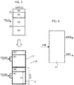
- Figures 5 and 6 are exemplary of possible criteria which may be adopted in mapping the RAM user space RAM US (receiving HAddr as an input) into the RAM physical space of the modules 11, 12 with respective signals C1Addr and C2Addr fed to (e.g. input interfaces IF) of the modules 11 and 12 via the RAM controller 13.
- the RAM controller 13 may have an input port AHB and two respective output ports RAM0, RAM2 as shown in figure 6 .
- the addresses for the partitions R3/R4 intended to receive the parity bits PAR1, PAR2 may be generated by offsetting and dividing HAddr e.g. as exemplified in the following, where HAddr and MWEN denote AHB address and RAM write enable (e.g. active low), respectively.
- PO En R4 ⁇ Reserved NO ACCESS NO ACCESS 1.25KB
- PO Dis R4 ⁇ DATA DATA 0xA00 0xB3F NO ACCESS 0x2000 5000
- PO En R2 ⁇ DATA PARITY DATA 10KB 0x2000 4FFF 0xA00 0xB3F 0x000 0x9FF
- DO Dis R2 ⁇ DATA NO
Landscapes
- Engineering & Computer Science (AREA)
- Theoretical Computer Science (AREA)
- Quality & Reliability (AREA)
- Physics & Mathematics (AREA)
- General Engineering & Computer Science (AREA)
- General Physics & Mathematics (AREA)
- Techniques For Improving Reliability Of Storages (AREA)
- Communication Control (AREA)
- Detection And Correction Of Errors (AREA)
Abstract
In an embodiment, a method of managing memories (10) includes:
- providing a first (11) memory module and a second memory module (12) each including a first (R1, R2) and a second (R4, R3) partition,
- writing first data (DATA1) in the first partition (R1) of the first memory module (11) and second data (DATA2) in the first partition (R2) of the second memory module (12), and
- selectively operating the first (11) and second (12) memory modules in a first operating mode or a second operating mode, where:
- in the first operating mode, parity bits (PAR1) for the first data (DATA1) are written in the second partition (R3) of the second memory module (12) and parity bits (PAR2) for the second data (DATA2) are written in the second partition (R4) of the first memory module (11),
- in the second operating mode, further data (ED1, ED2) are written in the place of parity bits (PAR1, PAR2) in the second partition (R4, R3) of one or both the first memory module (11) and the second memory module (12).
- providing a first (11) memory module and a second memory module (12) each including a first (R1, R2) and a second (R4, R3) partition,
- writing first data (DATA1) in the first partition (R1) of the first memory module (11) and second data (DATA2) in the first partition (R2) of the second memory module (12), and
- selectively operating the first (11) and second (12) memory modules in a first operating mode or a second operating mode, where:
- in the first operating mode, parity bits (PAR1) for the first data (DATA1) are written in the second partition (R3) of the second memory module (12) and parity bits (PAR2) for the second data (DATA2) are written in the second partition (R4) of the first memory module (11),
- in the second operating mode, further data (ED1, ED2) are written in the place of parity bits (PAR1, PAR2) in the second partition (R4, R3) of one or both the first memory module (11) and the second memory module (12).
Description
- The description relates to managing memories.
- One or more embodiments may apply to managing semiconductor memories such as e.g. embedded RAMs.
- Management of semiconductor memories such as parity management in embedded RAMs, as used e.g. in MicroController Units - MCUs, Systems-on-Chip - SoCs, may be a key factor in certain applications and be hardly of interest for other applications.
- Dedicating a part of a memory array to parity management (e.g. with words by 36 bits for 32 bit data, words by 72 bits for 64 bit data, and so on) may add to the cost of a memory array, also in terms of die size and semiconductor module, with the risk that these added cost factors may turn out to be unjustified for those applications that do not take advantage of them.
- The need is therefore felt for improved arrangements which may overcome the drawbacks outlined in the foregoing.
- An object of one or more embodiments is to provide a response to that need.
- According to one or more embodiments, such an object may be achieved by means of a method having the features set forth in the claims that follow.
- One or more embodiments may relate to a corresponding memory device (e.g. a memory array) and a corresponding apparatus (such as a MCU, a SoC, and so on) including such a device.
- The claims are an integral part of the disclosure of one or more exemplary embodiments as provided herein.
- One or more embodiments may provide memories such as RAMs offering adequate performance at e.g. one data word for clock cycle.
- One or more embodiments may involve building a dual-memory (e.g. dual RAM) structure adapted to be used in a flexible manner by selectively devoting at least a portion of the memory either to parity or data.
- One or more embodiments will now be described, by way of example only, with reference to the annexed figures, wherein:
-
Figure 1 is exemplary of memory management according to one or more embodiments; -
Figure 2 is further exemplary of memory management according to one or more embodiments; -
Figure 3 is a functional block diagram exemplary of a hardware arrangement according to one or more embodiments; -
Figures 4 to 6 provide further details of possible management of memories according to one or more embodiments; and -
Figure 7 is exemplary of possible dimensioning of a memory according to one or more embodiments. - In the ensuing description one or more specific details are illustrated, aimed at providing an in-depth understanding of examples of embodiments. The embodiments may be obtained without one or more of the specific details, or with other methods, components, materials, etc. In other cases, known structures, materials, or operations are not illustrated or described in detail so that certain aspects of embodiments will not be obscured.
- Reference to "an embodiment" or "one embodiment" in the framework of the present description is intended to indicate that a particular configuration, structure, or characteristic described in relation to the embodiment is comprised in at least one embodiment. Hence, phrases such as "in an embodiment" or "in one embodiment" that may be present in one or more points of the present description do not necessarily refer to one and the same embodiment. Moreover, particular conformations, structures, or characteristics may be combined in any adequate way in one or more embodiments.
- The references used herein are provided merely for convenience and hence do not define the extent of protection or the scope of the embodiments.
- In the figures,
reference 10 denotes a memory such as a semiconductor memory. - A RAM is exemplary of a memory to which one or more embodiments may apply.
- In one or more embodiments, the
memory 10 may be arranged to include a first memory module 11 (CUT1) and a second memory module 12 (CUT2). - Designating the
memory modules second memory modules memory modules - In one or more embodiments each
memory module - For instance, the
memory module 11 may include a first partition R1 and a second partition R4 while thesecond memory module 12 may include a first partition R2 and a second partition R3. - In one or more embodiments, the
memory 10 may be configured (in a manner known per se, and possibly as further detailed in the following) so that: - first data DATA1 may be written into (and correspondingly read from) the first partition R1 of the
first memory module 11, and - second data DATA2 may be written into (and correspondingly read from) the first partition R2 of the
second memory module 12. - Also, one or more embodiments may envisage operating the first and
second memory modules 11 and 12: - in a first operating mode, wherein parity bits PAR1 for the first data DATA1 are written in the second partition R3 of the
second memory module 12 while parity bits PAR2 for the second data DATA2 are written in the second partition R4 of thefirst memory module 11, and - in at least one second operating mode, wherein at least one (e.g. one or both) of the second partitions R3, R4 in the
memory modules -
Figure 2 is a comparative representation showing: - on the left-hand side, a first operating mode where the second partition R4, R3 of the
memory modules 11 are used to store parity bits PAR1, PAR2 for the data DATA1, DATA2 stored in the first partitions R1, R2; and - on the right-hand side, a second operating mode where the second partitions R4, R3 of both
modules - The two portions (left-side and right-side) of
Figure 2 may be regarded as exemplary of how, in one or more embodiments a memory space (e.g. RAM) may be seen by a user (i.e. by software) in two cases of parity enabled and parity disabled. - In one or more embodiments a "cross-wise" structure as detailed in the following was found to be adequate for implementing a configurable parity feature, possibly by resorting to address remapping, that is to translating user addresses into physical addresses mapped on R1/R2/R3/R4.
- One or more embodiments may be configured to implement a "cross-wise" write (and read) arrangement such that:
- parity bits PAR1 for the data DATA1 stored in the first memory module 11 (partition R1) are stored in the second memory module 12 (partition R3) and, correspondingly
- parity bits PAR2 for the data DATA2 stored in the second memory module 12 (partition R2) are stored in the first memory module 11 (partition R4).
- In one or more embodiments, storing extra data ED1, ED2 in memory space R3, R4 otherwise usable for parity bits may involve using the same word size.
- In one or more embodiments, the two
memory modules modules - In one or more embodiments, the first partitions R1, R2 and the second partitions R4, R3 can be mutually dimensioned with the second partitions R4, R3 having a size ES which is a sub-multiple of the size DS of the first partitions R1, R2, e.g. DS/8.
- In one or more such embodiments a one parity word may thus be coupled to 8 data words.
- In one or more embodiments, operation may be based on 32-bit words with one parity word associated to 8 data words that is with a write mask having a bit granularity adequate to support data write bites.
- Different dimensioning options may be applied in one or more embodiments.
- In one or more embodiments write events in the partitions R3, R4 may generate access errors if parity is enabled (see e.g. left-hand side of
Figure 2 and the signal OB inFigure 3 ). - The functional block diagram of
Figure 3 is exemplary of the possibility of managing various operating modes as exemplified in the foregoing by hardware, that is with aRAM control module 13 configured to switch the memory 10 (including themodules 11, 12) to different operating modes e.g. based on option bits OB as possibly stored in anon-volatile memory 14. - In one or more embodiments, the
memory 14 may be configured e.g. to receive an external parity option signal PO indicating whether parity bit operation is intended to be adopted in thememory modules control module 15 for thenon-volatile memory 14. - In one or more embodiments the
control modules CPU 16. - One or more embodiments as exemplified in
Figure 3 therefore permit parity bits write to be fully managed by hardware without giving rise to RAM bandwidth limitations. - The diagram of
Figure 4 is exemplary of the possibility of achieving full bandwidth by means of a symmetrical dual-RAM structure - In one or more embodiments, such parallel operation may be made possible by the "cross-wise" write arrangement already discussed in the foregoing which provides for DATA1 stored in partition R1 of
module 11 having their respective parity bits PAR1 stored in partition R3 ofmodule 12 while DATA2 stored in partition R2 ofmodule 12 have their respective parity bits PAR2 stored in partition R4 ofmodule 11. - The left hand side of the diagram of
Figure 4 is exemplary of how the various partitions R1, R2, R3, R4 of thememory modules controller 13. - The exemplary representation of
Figure 4 (where the assumption is again made that the twomodules - In one or more embodiments, the
RAM controller 13 may be configured to drive the twomemory modules module 11 or CUT1 and C2Addr for themodule 12 or CUT2, possibly with address re-mapping (HAddr). - In one or more embodiments as=log2(SIZE) may represent the number of address bits of C1Addr and C2Addr, where SIZE is the number of words and S1 denotes the size of the partitions R1 and R2 in number of words (which may be derived from SIZE) and start_HAddr may represent a start user space address which may be assumed to be aligned to SIZE.
-
Figures 5 and 6 are exemplary of possible criteria which may be adopted in mapping the RAM user space RAM US (receiving HAddr as an input) into the RAM physical space of themodules modules RAM controller 13. - As depicted in
Figure 6 theRAM controller 13 may have an input port AHB and two respective output ports RAM0, RAM2 as shown infigure 6 . - By way of example, in an operational mode providing for parity bit management (PO=enabled) the addresses for the partitions R3/R4 intended to receive the parity bits PAR1, PAR2 may be generated by offsetting and dividing HAddr e.g. as exemplified in the following, where HAddr and MWEN denote AHB address and RAM write enable (e.g. active low), respectively.
HAddr belongs to R1 → C1Addr = HAddr(as + 1:2) MWEN = f1 (HAddr (1:0) ,HSIZE) C2Addr = S1 + C1Addr(as - 1:3) MWEN = f2 (HAddr (4:0) ,HSIZE) HAddr belongs to R2 → Haddr' = Haddr - S1*4 C1Addr = S1 + C2Addr(as - 1:3) MWEN = f2 (HAddr' (4:0) ,HSIZE) C2Addr = HAddr'(as + 1:2) MWEN = f1 (HAddr' (1:0) ,HSIZE) HAddr belongs to R3/R4 → ERROR - In a mode of operation providing for the partitions R3/R4 being used for data storage (and not for storing parity bits) only one module or cut may be accessed per time e.g. based on the following approach.
HAddr belongs to R1 → C1Addr = HAddr(as + 1:2) MWEN = f1 (HAddr (1:0) ,HSIZE) HAddr Haddr' = Haddr - S1*4 belongs to R2/R3 → C2Addr = HAddr'(as + 1:2) MWEN = f1 (HAddr' (1:0) ,HSIZE) HAddr belongs to R4 → Haddr' = Haddr - SIZE*4 C1Addr = HAddr'(as + 1:2) MWEN = f1 (HAddr' (1:0) ,HSIZE) -
Figure 7 is exemplary of a possible arrangement of a memory map as per the memory map reproduced in the following, where PO=En and PO=Dis denote Parity 5 Operation enabled and disabled, respectively.MAPPING ADDRESS OPTION DESCRIPTION CUT1 CUT2 SIZE 0x2000 5500 PO=En R4→Reserved NO ACCESS NO ACCESS 1.25KB SRAM 0x2000 59FF PO=Dis R4→ DATA DATA 0xA00 0xB3F NO ACCESS 0x2000 5000 PO=En R3→Reserved NO ACCESS NO ACCESS 1.25KB 0x2000 54FF PO=Dis R3→ DATA NO ACCESS DATA 0xA00 0xB3F 0x2000 2800 PO=En R2→ DATA PARITY DATA 10KB 0x2000 4FFF 0xA00 0xB3F 0x000 0x9FF PO=Dis R2→ DATA NO ACCESS DATA 0x000 0x9FF 0x2000 0000 PO=En R1→ DATA DATA PARITY 10KB 0x2000 27FF 0x000 0x9FF 0xA00 0xB3F PO=Dis R1→ DATA DATA 0x000 0x9FF NO ACCESS - Without prejudice to the underlying principles, the details and embodiments may vary, even significantly, with respect to what has been described by way of example only, without departing from the extent of protection.
- The extent of protection is determined by the claims that follow.
Claims (10)
- A method of managing memories (10) including:- providing a first (11) memory module and a second memory module (12) including respective first (R1, R2) and second (R4, R3) partitions,- writing first data (DATA1) in the first partition (R1) of the first memory module (11) and second data (DATA2) in the first partition (R2) of the second memory module (12),
the method further including selectively (OB) operating said first (11) and second (12) memory modules in a first operating mode or at least one second operating mode, wherein:- in said first operating mode, parity bits (PAR1) for said first data (DATA1) are written in the second partition (R3) of the second memory module (12) and parity bits (PAR2) for said second data (DATA2) are written in the second partition (R4) of the first memory module (11),- in said at least one second operating mode, further data (ED1, ED2) are written in the place of parity bits (PAR1, PAR2) in the second partition (R4, R3) of at least one of the first memory module (11) and the second memory module (12). - The method of claim 1, wherein in said at least one second operating mode further data (ED1, ED2) are written in the place of parity bits (PAR1, PAR2) in the second partitions (R4, R3) of both of the first memory module (11) and the second memory module (12).
- The method of claim 1 or claim 2, including selecting said first (11) and second (12) memory modules of a same size (DS, ES).
- The method of any of the previous claims, including selecting the size of said second partitions (R4, R3) as a sub-multiple, preferably equal to 1/8, of the size of said first partitions (R1, R2).
- The method of any of the previous claims, wherein said parity bits (PAR1, PAR2) include one parity word to 8 data words in said first partitions (R1, R2).
- The method of any of the previous claims, including configuring said first (11) and second (12) memory modules for dual-port (C1Addr, C2Addr) parallel writes, preferably by means of address remapping (HAddr).
- A memory device (10), including:- a first (11) memory module and a second memory module (12) including respective first (R1, R2) and second (R4, R3) partitions,- a memory controller (13) configured for writing first data (DATA1) in the first partition (R1) of the first memory module (11) and second data (DATA2) in the first partition (R2) of the second memory module (12), the memory controller (13) configured for selectively (OB) operating said first (11) and second (12) memory modules in a first operating mode or at least one second operating mode, wherein:- in said first operating mode, parity bits (PAR1) for said first data (DATA1) are written in the second partition (R3) of the second memory module (12) and parity bits (PAR2) for said second data (DATA2) are written in the second partition (R4) of the first memory module (11),- in said at least one second operating mode further data (ED1, ED2) are written in the place of parity bits (PAR1, PAR2) in the second partition (R4, R3) of at least one of the first memory module (11) and the second memory module (12).
- The memory device of claim 7, wherein said memory controller (13) is configured for operating said first (11) and second (12) memory modules in a said at least one second operating mode wherein further data (ED1, ED2) are written in the place of parity bits (PAR1, PAR2) in the second partitions (R4, R3) of both of the first memory module (11) and the second memory module (12).
- The memory device of claim 7 or claim 8, having at least one of the following characteristics:- said first (11) and second (12) memory modules are of a same size (DS, ES),- the size of said second partitions (R4, R3) is a sub-multiple, preferably equal to 1/8, of the size of said first partitions (R1, R2),- said parity bits (PAR1, PAR2) include one parity word to 8 data words in said first partitions (R1, R2).- said memory controller (13) and said first (11) and second (12) memory modules are configured for dual-port (C1Addr, C2Addr) parallel writes, preferably by means of address remapping (HAddr).
- Apparatus, preferably a MicroController Unit - MCU or a System-on-Chip - SoC, including the memory device of any of claims 7 to 9.
Applications Claiming Priority (1)
| Application Number | Priority Date | Filing Date | Title |
|---|---|---|---|
| ITUB2015A003367A ITUB20153367A1 (en) | 2015-09-03 | 2015-09-03 | PROCEDURE FOR THE MANAGEMENT OF MEMORIES, EQUIPMENT AND CORRESPONDING EQUIPMENT |
Publications (1)
| Publication Number | Publication Date |
|---|---|
| EP3139275A1 true EP3139275A1 (en) | 2017-03-08 |
Family
ID=54705747
Family Applications (1)
| Application Number | Title | Priority Date | Filing Date |
|---|---|---|---|
| EP16162366.5A Withdrawn EP3139275A1 (en) | 2015-09-03 | 2016-03-24 | Method of managing memories, corresponding device and apparatus |
Country Status (3)
| Country | Link |
|---|---|
| US (1) | US9823965B2 (en) |
| EP (1) | EP3139275A1 (en) |
| IT (1) | ITUB20153367A1 (en) |
Citations (3)
| Publication number | Priority date | Publication date | Assignee | Title |
|---|---|---|---|---|
| WO2007100694A2 (en) * | 2006-02-27 | 2007-09-07 | Intel Corporation | Systems, methods, and apparatuses for using the same memory type to support an error check mode and a non-error check mode |
| US20080005646A1 (en) * | 2006-06-30 | 2008-01-03 | Bains Kuljit S | Reliability, availability, and serviceability in a memory device |
| WO2009121022A2 (en) * | 2008-03-28 | 2009-10-01 | Intel Corporation | Systems, methods, and apparatuses to save memory self-refresh power |
Family Cites Families (2)
| Publication number | Priority date | Publication date | Assignee | Title |
|---|---|---|---|---|
| US20140063983A1 (en) * | 2012-09-06 | 2014-03-06 | International Business Machines Corporation | Error Detection And Correction In A Memory System |
| US9354973B2 (en) * | 2013-03-13 | 2016-05-31 | Intel Corporation | Data integrity management in memory systems |
-
2015
- 2015-09-03 IT ITUB2015A003367A patent/ITUB20153367A1/en unknown
-
2016
- 2016-03-24 EP EP16162366.5A patent/EP3139275A1/en not_active Withdrawn
- 2016-03-24 US US15/080,307 patent/US9823965B2/en active Active
Patent Citations (3)
| Publication number | Priority date | Publication date | Assignee | Title |
|---|---|---|---|---|
| WO2007100694A2 (en) * | 2006-02-27 | 2007-09-07 | Intel Corporation | Systems, methods, and apparatuses for using the same memory type to support an error check mode and a non-error check mode |
| US20080005646A1 (en) * | 2006-06-30 | 2008-01-03 | Bains Kuljit S | Reliability, availability, and serviceability in a memory device |
| WO2009121022A2 (en) * | 2008-03-28 | 2009-10-01 | Intel Corporation | Systems, methods, and apparatuses to save memory self-refresh power |
Also Published As
| Publication number | Publication date |
|---|---|
| ITUB20153367A1 (en) | 2017-03-03 |
| US20170068594A1 (en) | 2017-03-09 |
| US9823965B2 (en) | 2017-11-21 |
Similar Documents
| Publication | Publication Date | Title |
|---|---|---|
| US10365844B2 (en) | Logical block address to physical block address (L2P) table compression | |
| US7243203B2 (en) | Pipeline circuit for low latency memory | |
| US8656252B2 (en) | Memory controller and non-volatile storage device | |
| EP1989712B1 (en) | Systems, methods, and apparatuses for using the same memory type to support an error check mode and a non-error check mode | |
| JP4628750B2 (en) | Flash memory device with built-in buffer memory and flash memory system | |
| US20120239863A1 (en) | Nonvolatile memory systems with embedded fast read and write memories | |
| US8316175B2 (en) | High throughput flash memory system | |
| US11114138B2 (en) | Data structures with multiple read ports | |
| US8122199B2 (en) | Multi port memory device with shared memory area using latch type memory cells and driving method | |
| CN102414669B (en) | Multi-port memory device and method | |
| CN106528443A (en) | FLASH management system and method suitable for satellite-borne data management | |
| US20230223065A1 (en) | Memory device, memory module, and operating method of memory device for processing in memory | |
| US20090157949A1 (en) | Address translation between a memory controller and an external memory device | |
| US9773571B2 (en) | Memory repair redundancy with array cache redundancy | |
| US11550658B1 (en) | Storage system and method for storing logical-to-physical address table entries in a codeword in volatile memory | |
| US10216685B1 (en) | Memory modules with nonvolatile storage and rapid, sustained transfer rates | |
| EP3038109A1 (en) | Pseudo dual port memory using a dual port cell and a single port cell with associated valid data bits and related methods | |
| US9823965B2 (en) | Method of managing memories, corresponding device and apparatus | |
| US20100262754A1 (en) | Cpu data bus pld/fpga interface using dual port ram structure built in pld | |
| US7715271B1 (en) | Using dedicated read output path to reduce unregistered read access time for a FPGA embedded memory | |
| US7259989B2 (en) | Non-volatile memory device | |
| TW201947403A (en) | Data storage apparatus and system information programming mehtod | |
| US20250174267A1 (en) | Memory device and system, and decoding circuit | |
| TW202121425A (en) | Data storage device and non-volatile memory control method | |
| US20230062773A1 (en) | Nonvolatile memory and memory system |
Legal Events
| Date | Code | Title | Description |
|---|---|---|---|
| PUAI | Public reference made under article 153(3) epc to a published international application that has entered the european phase |
Free format text: ORIGINAL CODE: 0009012 |
|
| AK | Designated contracting states |
Kind code of ref document: A1 Designated state(s): AL AT BE BG CH CY CZ DE DK EE ES FI FR GB GR HR HU IE IS IT LI LT LU LV MC MK MT NL NO PL PT RO RS SE SI SK SM TR |
|
| AX | Request for extension of the european patent |
Extension state: BA ME |
|
| STAA | Information on the status of an ep patent application or granted ep patent |
Free format text: STATUS: THE APPLICATION IS DEEMED TO BE WITHDRAWN |
|
| 18D | Application deemed to be withdrawn |
Effective date: 20170909 |