EP3136440A1 - Organic light emitting display device and method of manufacturing the same - Google Patents
Organic light emitting display device and method of manufacturing the same Download PDFInfo
- Publication number
- EP3136440A1 EP3136440A1 EP16177761.0A EP16177761A EP3136440A1 EP 3136440 A1 EP3136440 A1 EP 3136440A1 EP 16177761 A EP16177761 A EP 16177761A EP 3136440 A1 EP3136440 A1 EP 3136440A1
- Authority
- EP
- European Patent Office
- Prior art keywords
- electrode
- contact
- anode
- auxiliary
- protection
- Prior art date
- Legal status (The legal status is an assumption and is not a legal conclusion. Google has not performed a legal analysis and makes no representation as to the accuracy of the status listed.)
- Granted
Links
Images




Classifications
-
- H—ELECTRICITY
- H10—SEMICONDUCTOR DEVICES; ELECTRIC SOLID-STATE DEVICES NOT OTHERWISE PROVIDED FOR
- H10K—ORGANIC ELECTRIC SOLID-STATE DEVICES
- H10K59/00—Integrated devices, or assemblies of multiple devices, comprising at least one organic light-emitting element covered by group H10K50/00
- H10K59/10—OLED displays
- H10K59/12—Active-matrix OLED [AMOLED] displays
- H10K59/122—Pixel-defining structures or layers, e.g. banks
-
- H—ELECTRICITY
- H10—SEMICONDUCTOR DEVICES; ELECTRIC SOLID-STATE DEVICES NOT OTHERWISE PROVIDED FOR
- H10K—ORGANIC ELECTRIC SOLID-STATE DEVICES
- H10K50/00—Organic light-emitting devices
- H10K50/80—Constructional details
- H10K50/805—Electrodes
- H10K50/81—Anodes
- H10K50/814—Anodes combined with auxiliary electrodes, e.g. ITO layer combined with metal lines
-
- H—ELECTRICITY
- H10—SEMICONDUCTOR DEVICES; ELECTRIC SOLID-STATE DEVICES NOT OTHERWISE PROVIDED FOR
- H10K—ORGANIC ELECTRIC SOLID-STATE DEVICES
- H10K50/00—Organic light-emitting devices
- H10K50/80—Constructional details
- H10K50/805—Electrodes
- H10K50/82—Cathodes
- H10K50/824—Cathodes combined with auxiliary electrodes
-
- H—ELECTRICITY
- H10—SEMICONDUCTOR DEVICES; ELECTRIC SOLID-STATE DEVICES NOT OTHERWISE PROVIDED FOR
- H10K—ORGANIC ELECTRIC SOLID-STATE DEVICES
- H10K50/00—Organic light-emitting devices
- H10K50/80—Constructional details
- H10K50/805—Electrodes
- H10K50/82—Cathodes
- H10K50/828—Transparent cathodes, e.g. comprising thin metal layers
-
- H—ELECTRICITY
- H10—SEMICONDUCTOR DEVICES; ELECTRIC SOLID-STATE DEVICES NOT OTHERWISE PROVIDED FOR
- H10K—ORGANIC ELECTRIC SOLID-STATE DEVICES
- H10K59/00—Integrated devices, or assemblies of multiple devices, comprising at least one organic light-emitting element covered by group H10K50/00
- H10K59/10—OLED displays
- H10K59/12—Active-matrix OLED [AMOLED] displays
- H10K59/123—Connection of the pixel electrodes to the thin film transistors [TFT]
-
- H—ELECTRICITY
- H10—SEMICONDUCTOR DEVICES; ELECTRIC SOLID-STATE DEVICES NOT OTHERWISE PROVIDED FOR
- H10K—ORGANIC ELECTRIC SOLID-STATE DEVICES
- H10K59/00—Integrated devices, or assemblies of multiple devices, comprising at least one organic light-emitting element covered by group H10K50/00
- H10K59/10—OLED displays
- H10K59/12—Active-matrix OLED [AMOLED] displays
- H10K59/124—Insulating layers formed between TFT elements and OLED elements
-
- H—ELECTRICITY
- H10—SEMICONDUCTOR DEVICES; ELECTRIC SOLID-STATE DEVICES NOT OTHERWISE PROVIDED FOR
- H10K—ORGANIC ELECTRIC SOLID-STATE DEVICES
- H10K59/00—Integrated devices, or assemblies of multiple devices, comprising at least one organic light-emitting element covered by group H10K50/00
- H10K59/10—OLED displays
- H10K59/12—Active-matrix OLED [AMOLED] displays
- H10K59/126—Shielding, e.g. light-blocking means over the TFTs
-
- H—ELECTRICITY
- H10—SEMICONDUCTOR DEVICES; ELECTRIC SOLID-STATE DEVICES NOT OTHERWISE PROVIDED FOR
- H10K—ORGANIC ELECTRIC SOLID-STATE DEVICES
- H10K59/00—Integrated devices, or assemblies of multiple devices, comprising at least one organic light-emitting element covered by group H10K50/00
- H10K59/10—OLED displays
- H10K59/12—Active-matrix OLED [AMOLED] displays
- H10K59/131—Interconnections, e.g. wiring lines or terminals
- H10K59/1315—Interconnections, e.g. wiring lines or terminals comprising structures specially adapted for lowering the resistance
-
- H—ELECTRICITY
- H10—SEMICONDUCTOR DEVICES; ELECTRIC SOLID-STATE DEVICES NOT OTHERWISE PROVIDED FOR
- H10K—ORGANIC ELECTRIC SOLID-STATE DEVICES
- H10K59/00—Integrated devices, or assemblies of multiple devices, comprising at least one organic light-emitting element covered by group H10K50/00
- H10K59/80—Constructional details
- H10K59/805—Electrodes
- H10K59/8052—Cathodes
- H10K59/80522—Cathodes combined with auxiliary electrodes
-
- H—ELECTRICITY
- H10—SEMICONDUCTOR DEVICES; ELECTRIC SOLID-STATE DEVICES NOT OTHERWISE PROVIDED FOR
- H10K—ORGANIC ELECTRIC SOLID-STATE DEVICES
- H10K71/00—Manufacture or treatment specially adapted for the organic devices covered by this subclass
-
- H—ELECTRICITY
- H10—SEMICONDUCTOR DEVICES; ELECTRIC SOLID-STATE DEVICES NOT OTHERWISE PROVIDED FOR
- H10K—ORGANIC ELECTRIC SOLID-STATE DEVICES
- H10K71/00—Manufacture or treatment specially adapted for the organic devices covered by this subclass
- H10K71/621—Providing a shape to conductive layers, e.g. patterning or selective deposition
-
- H—ELECTRICITY
- H10—SEMICONDUCTOR DEVICES; ELECTRIC SOLID-STATE DEVICES NOT OTHERWISE PROVIDED FOR
- H10K—ORGANIC ELECTRIC SOLID-STATE DEVICES
- H10K2102/00—Constructional details relating to the organic devices covered by this subclass
- H10K2102/10—Transparent electrodes, e.g. using graphene
- H10K2102/101—Transparent electrodes, e.g. using graphene comprising transparent conductive oxides [TCO]
- H10K2102/103—Transparent electrodes, e.g. using graphene comprising transparent conductive oxides [TCO] comprising indium oxides, e.g. ITO
-
- H—ELECTRICITY
- H10—SEMICONDUCTOR DEVICES; ELECTRIC SOLID-STATE DEVICES NOT OTHERWISE PROVIDED FOR
- H10K—ORGANIC ELECTRIC SOLID-STATE DEVICES
- H10K2102/00—Constructional details relating to the organic devices covered by this subclass
- H10K2102/301—Details of OLEDs
- H10K2102/302—Details of OLEDs of OLED structures
- H10K2102/3023—Direction of light emission
- H10K2102/3026—Top emission
-
- H—ELECTRICITY
- H10—SEMICONDUCTOR DEVICES; ELECTRIC SOLID-STATE DEVICES NOT OTHERWISE PROVIDED FOR
- H10K—ORGANIC ELECTRIC SOLID-STATE DEVICES
- H10K50/00—Organic light-emitting devices
- H10K50/80—Constructional details
- H10K50/805—Electrodes
- H10K50/81—Anodes
- H10K50/818—Reflective anodes, e.g. ITO combined with thick metallic layers
-
- H—ELECTRICITY
- H10—SEMICONDUCTOR DEVICES; ELECTRIC SOLID-STATE DEVICES NOT OTHERWISE PROVIDED FOR
- H10K—ORGANIC ELECTRIC SOLID-STATE DEVICES
- H10K59/00—Integrated devices, or assemblies of multiple devices, comprising at least one organic light-emitting element covered by group H10K50/00
- H10K59/10—OLED displays
- H10K59/12—Active-matrix OLED [AMOLED] displays
- H10K59/1201—Manufacture or treatment
-
- H—ELECTRICITY
- H10—SEMICONDUCTOR DEVICES; ELECTRIC SOLID-STATE DEVICES NOT OTHERWISE PROVIDED FOR
- H10K—ORGANIC ELECTRIC SOLID-STATE DEVICES
- H10K59/00—Integrated devices, or assemblies of multiple devices, comprising at least one organic light-emitting element covered by group H10K50/00
- H10K59/80—Constructional details
- H10K59/805—Electrodes
- H10K59/8051—Anodes
- H10K59/80516—Anodes combined with auxiliary electrodes, e.g. ITO layer combined with metal lines
Definitions
- Embodiments of the present disclosure relate to an organic light emitting display device, and more particularly, to a top emission type organic light emitting display device, and a method of manufacturing the same.
- OLED organic light emitting display
- the OLED device may be largely classified into a top emission type and a bottom emission type.
- a circuit device is disposed between an emitting layer and an image displaying surface, whereby an aperture ratio may be lowered due to the circuit device.
- a circuit device is not disposed between an emitting layer and an image displaying surface, whereby an aperture ratio may be improved.
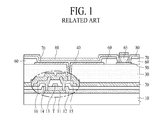
- FIG. 1 is a cross sectional view of a related art top emission type OLED device.
- a thin film transistor layer (T) including an active layer 11, a gate insulating film 12, a gate electrode 13, an insulating interlayer 14, a source electrode 15, and a drain electrode 16 is provided on a substrate 10, and then a passivation layer 20 and a planarization layer 30 are sequentially provided on the thin film transistor layer (T).
- an anode electrode 40 and an auxiliary electrode 50 are provided on the planarization layer 30.
- the auxiliary electrode 50 is provided to reduce a resistance of a cathode electrode 80 to be explained later.
- a bank 60 is provided to define a pixel region. Also, an organic emitting layer 70 is provided in the pixel region defined by the bank 60, and the cathode electrode 80 is provided on the organic emitting layer 70.
- the cathode electrode 80 is formed of a transparent conductive material, which causes the increase of resistance therein. In order to reduce the resistance of the cathode electrode 80, the cathode electrode 80 is connected with the auxiliary electrode 50.
- an upper surface of the auxiliary electrode 50 is not covered by the organic emitting layer 70. That is, after forming the organic emitting layer 70, the upper surface of the auxiliary electrode 50 is exposed so that the cathode electrode 80 is connected with the upper surface of the auxiliary electrode 50.
- a partition 65 with a reversed tapered structure is provided in the upper surface of the auxiliary electrode 50.
- the partition 65 with the reversed tapered structure serves as eaves, whereby the organic emitting layer 70 is not deposited in the space. That is, the organic emitting layer 70 may be manufactured by a deposition process using a deposition material with superior straightness, for example, evaporation.
- the partition 65 serves as the eaves so that it is possible to prevent the organic emitting layer 70 from being deposited in the space between the bank 60 and the partition 65.
- the cathode electrode 80 may be manufactured by a deposition process using a deposition material with inferior straightness, for example, sputtering.
- the cathode electrode 80 may be deposited in the space between the bank 60 and the partition 65 so that the cathode electrode 80 may be electrically connected with the auxiliary electrode 50.
- the related art top emission type organic light emitting display device necessarily includes the partition 65 with the reversed tapered structure, it may have the following problems.
- the partition 65 In order to pattern the partition 65 with the reversed tapered structure, it is necessary to carry out a PEB (Post Exposure Bake) process. However, it is difficult to control the PEB process to obtain the desired reversed tapered structure. If the desired reversed tapered structure is not created, the partition 65 may collapse or peel off. In this case, an electrical connection between the cathode electrode 80 and the auxiliary electrode 50 may be difficult.
- PEB Post Exposure Bake
- embodiments of the present disclosure are directed to a top emission type organic light emitting display device that substantially obviates one or more problems due to limitations and disadvantages of the related art.
- An aspect of the present disclosure is directed to provide a top emission type organic light emitting display device which facilitates an electrical connection between a cathode electrode and an auxiliary electrode without a partition having a reversed tapered structure.
- an organic light emitting display device may include an anode electrode on a substrate; an organic emitting layer on the anode electrode; a cathode electrode on the organic emitting layer; an auxiliary electrode electrically connected with the cathode electrode; and a contact electrode that is on a same layer as the auxiliary electrode, the contact electrode horizontally spaced apart from the auxiliary electrode, the contact electrode directly connected with both the auxiliary electrode and the cathode electrode to connect together the auxiliary electrode and a portion of the cathode electrode that is on a same layer as the auxiliary electrode.
- a method of manufacturing an organic light emitting display device may include forming a contact electrode over a substrate, the contact electrode including a first contact electrode, a second contact electrode on the first contact electrode, and a third contact electrode on the second contact electrode, the first contact electrode formed with an end that horizontally extends past an end of the third contact electrode; forming a planarization layer over the contact electrode, the planarization layer including a contact hole that exposes the contact electrode; forming a protection electrode on the planarization layer, the protection electrode connected to the contact electrode via the contact hole in the planarization layer; forming a bank that overlaps a portion of the protection electrode, a portion of the first contact electrode, a portion of the second contact electrode, and the end of the third contact electrode; etching a portion of the protection electrode and a portion of the second contact electrode that are not overlapped by the bank to create a hollow space between the portion of the second contact electrode and the portion of the first contact electrode that are overlapped by the bank; and
- an organic light emitting display device comprises: an anode electrode on a substrate; an organic emitting layer on the anode electrode; a cathode electrode on the organic emitting layer; an auxiliary electrode electrically connected with the cathode electrode; and a contact electrode that is on a same layer as the auxiliary electrode, the contact electrode horizontally spaced apart from the auxiliary electrode, the contact electrode directly connected with both the auxiliary electrode and the cathode electrode to connect together the auxiliary electrode and a portion of the cathode electrode that is on a same layer as the auxiliary electrode.
- the contact electrode may include a first contact electrode and a second contact electrode that is positioned over the first contact electrode.
- the second contact electrode may include a step-shaped portion that overlaps a portion of the first contact electrode, the step-shaped portion of the second contact electrode and the overlapped portion of the first contact electrode forming a hollow space between the step-shaped portion of the second electrode and the overlapped portion of the first contact electrode.
- a portion of the cathode electrode may extend to the hollow space in the layer including the auxiliary electrode and the contact electrode, and the cathode electrode may directly connect to the first contact electrode.
- the step-shaped portion may include a vertical portion and a horizontal portion connected to the vertical portion, the horizontal portion substantially parallel with the substrate.
- An end of the first contact electrode may horizontally extend past an end of the second contact electrode in a direction away from the auxiliary electrode.
- the auxiliary electrode may further comprise: a first auxiliary electrode; a second auxiliary electrode on the first auxiliary electrode; and a third auxiliary electrode on the second auxiliary electrode, wherein the first auxiliary electrode is connected to the first contact electrode, and the third auxiliary electrode is connected to the second contact electrode.
- a thickness of the second auxiliary electrode may be greater than thicknesses of the first auxiliary electrode and the third auxiliary electrode, the first auxiliary electrode and the third auxiliary electrode may have a higher resistance to corrosion than the second auxiliary electrode, and the third auxiliary electrode may cover an upper surface and side surfaces of the second auxiliary electrode.
- the organic light emitting display device may further comprise a protection electrode positioned on the second contact electrode, wherein an end of the first contact electrode horizontally extends past an end of the protection electrode.
- the protection electrode may comprise: a first protection electrode; a second protection electrode on the first protection electrode; and a third protection electrode on the second protection electrode, wherein the first protection electrode and the third protection electrode have a higher resistance to corrosion than the second protection electrode, and wherein a thickness of the second protection electrode is greater than thicknesses of the first protection electrode and the third protection electrode.
- the anode electrode may comprise: a first anode electrode, wherein a portion of the first anode electrode is in a same layer as the auxiliary electrode and the contact electrode; and a second anode electrode over the first anode electrode, the second anode electrode directly connected with the first anode electrode via a contact hole.
- Each of the first anode electrode and the second anode electrode may comprise: a first anode electrode portion; a second anode electrode portion on the first anode electrode portion; and a third anode electrode portion on the second anode electrode portion, wherein the first anode electrode portion and the third anode electrode portion have a higher resistance to corrosion than the second anode electrode portion; and wherein a thickness of the second anode electrode portion is greater than thicknesses of the first anode electrode portion and the third anode electrode portion.
- the organic light emitting display device may further comprise a planarization layer over the auxiliary electrode, and the contact electrode, the planarization layer including a contact hole that exposes the contact electrode, wherein the contact hole extends to the hollow space formed between the step-shaped portion of the second electrode and the overlapped portion of the first contact electrode.
- the organic light emitting display device may further comprise: a bank over the hollow space and on the planarization layer.
- the contact electrode may be made of a material that is resistance to etchant compared to a material of the protection electrode.
- a method of manufacturing an organic light emitting display device comprises: forming a contact electrode over a substrate, the contact electrode including a first contact electrode, a second contact electrode on the first contact electrode, and a third contact electrode on the second contact electrode, the first contact electrode formed with an end that horizontally extends past an end of the third contact electrode; forming a planarization layer over the contact electrode, the planarization layer including a contact hole that exposes the contact electrode; forming a protection electrode on the planarization layer, the protection electrode connected to the contact electrode via the contact hole in the planarization layer; forming a bank that overlaps a portion of the protection electrode, a portion of the first contact electrode, a portion of the second contact electrode, and the end of the third contact electrode; etching a portion of the protection electrode and a portion of the second contact electrode that are not overlapped by the bank to create a hollow space between the portion of the third contact electrode and the portion of the first contact electrode that are overlapped by the bank; and forming a cathode
- the method may further comprise: simultaneously forming an auxiliary electrode that is connected with the contact electrode and a first anode electrode in a same layer, the auxiliary electrode horizontally spaced apart from the first anode electrode, wherein the contact electrode is simultaneously formed with the auxiliary electrode and the first anode electrode.
- the method may further comprise: forming a second anode electrode that is connected with the first anode electrode, wherein a portion of the second anode electrode is formed in a different layer than the first anode electrode, wherein the second anode electrode and the protection electrode are simultaneously formed in a same layer.
- the method may further comprise: covering the second anode electrode with a mask before etching the portion of the protection electrode and the portion of the second contact electrode that is not overlapped by the bank.
- Etching may comprise: using an etchant to simultaneously remove the portion of the protection electrode and the portion of the second contact electrode that are not overlapped by the bank.
- a structure for example, an electrode, a line, a wiring, a layer, or a contact
- this description should be construed as including a case where the structures contact each other and moreover, a case where a third structure is disposed there between.
- first, second, etc. may be used herein to describe various elements, these elements should not be limited by these terms. These terms are only used to distinguish one element from another. For example, a first element could be termed a second element, and, similarly, a second element could be termed a first element, without departing from the scope of the present invention.
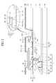
- FIG. 2 is a cross sectional view illustrating an organic light emitting display device according to one embodiment of the present disclosure.
- the organic light emitting display device may include a substrate 100, a thin film transistor layer (T), a passivation layer 165, a first planarization layer 171, a second planarization layer 172, a first anode electrode 180, a second anode electrode 200, an auxiliary electrode 190, a contact electrode 190a, a protection electrode 210, a bank 220, an organic emitting layer 240 and a cathode electrode 250.
- T thin film transistor layer
- passivation layer 165 a passivation layer 165
- a first planarization layer 171, a second planarization layer 172 a first anode electrode 180, a second anode electrode 200, an auxiliary electrode 190, a contact electrode 190a, a protection electrode 210, a bank 220, an organic emitting layer 240 and a cathode electrode 250.
- the substrate 100 may be formed of glass or transparent plastic.
- the thin film transistor layer (T) may include an active layer 110, a gate insulating film 120, a gate electrode 130, an insulating interlayer 140, a source electrode 150 and a drain electrode 160.
- the active layer 110 is provided on the substrate 100, wherein the active layer 110 overlaps with the gate electrode 130.
- the active layer 110 may be formed of a silicon-based semiconductor material or oxide-based semiconductor material.
- a light shielding layer may be additionally provided between the substrate 100 and the active layer 110. In this case, an external light, which is incident on a lower surface of the substrate 100, is blocked by the light shielding layer so that it is possible to prevent the active layer 110 from being damaged by the external light.
- the gate insulating film 120 is provided on the active layer 110.
- the gate insulating film 120 insulates the active layer 110 and the gate electrode 130 from each other.
- the gate insulating film 120 may be formed of an inorganic insulating material, and more particularly, the gate insulating film 120 may be formed in a single-layered structure of the inorganic insulating material such as silicon oxide SiOx or silicon nitride SiNx, or a multi-layered structure of the above silicon oxide SiOx and silicon nitride SiNx, but not limited to these structures.
- the gate electrode 130 is provided on the gate insulating film 120.
- the gate electrode 130 overlaps with the active layer 110, and the gate insulating film 120 is interposed between the gate electrode 130 and the active layer 110 being overlapped with each other.
- the gate electrode 130 may be formed in a single-layered structure or multi-layered structure including molybdenum (Mo), aluminum (Al), chrome or chromium (Cr), aurum or gold (Au), titanium (Ti), nickel (Ni), neodymium (Nd), copper (Cu) and their alloys, but not limited to these materials.
- the insulating interlayer 140 is provided on the gate electrode 130.
- the insulating interlayer 140 is formed of the same material as that of the gate insulating film 120.
- the insulating interlayer 140 may be formed in a single-layered structure of the inorganic insulating material such as silicon oxide SiOx or silicon nitride SiNx, or a multi-layered structure of the above silicon oxide SiOx, silicon nitride SiNx and their alloys, but not limited to these materials.
- the source electrode 150 and the drain electrode 160 confronting each other are provided on the insulating interlayer 140.
- a first contact hole (CH1) for exposing one end portion of the active layer 110 is provided in the aforementioned gate insulating film 120 and the insulating interlayer 140
- a second contact hole (CH2) for exposing the other end portion of the active layer 110 is provided in the aforementioned gate insulating film 120 and the insulating interlayer 140.
- the source electrode 150 is connected with the other end portion of the active layer 110 via the second contact hole (CH2)
- the drain electrode 160 is connected with one end portion of the active layer 110 via the first contact hole (CH1).
- the source electrode 150 may include a lower source electrode 151 and an upper source electrode 152.
- the lower source electrode 151 is provided between the insulating interlayer 140 and the upper source electrode 152, wherein the lower source electrode 151 enhances an adhesive strength between the insulating interlayer 140 and the upper source electrode 152. Also, the lower source electrode 151 protects a lower surface of the upper source electrode 152 so that it is possible to prevent the lower surface of the upper source electrode 152 from being corroded. Thus, an oxidation degree of the lower source electrode 151 may be lower than an oxidation degree of the upper source electrode 152. That is, a corrosion resistance in a material of the lower source electrode 151 may be superior to a corrosion resistance in a material of the upper source electrode 152.
- the lower source electrode 151 functions as an adhesion enhancement layer or a corrosion preventing layer.
- the lower source electrode 151 may be formed of an alloy MoTi of molybdenum and titanium, but not limited to this material.
- the upper source electrode 152 is provided on an upper surface of the lower source electrode 151.
- the upper source electrode 152 may be formed of a low-resistance metal material such as copper Cu, but not limited to this metal material.
- the upper source electrode 152 may be formed of a metal material whose resistance is relatively lower than that of the lower source electrode 151. In order to lower a total resistance of the source electrode 150, a thickness of the upper source electrode 152 may be larger than a thickness of the lower source electrode 151, preferably.
- the drain electrode 160 may include a lower drain electrode 161 and an upper drain electrode 162.
- the lower drain electrode 161 is provided between the insulating interlayer 140 and the upper drain electrode 162, wherein the lower drain electrode 161 enhances an adhesive strength between the insulating interlayer 140 and the upper drain electrode 162. Also, the lower drain electrode 161 prevents a lower surface of the upper drain electrode 162 from being corroded.
- an oxidation degree of the lower drain electrode 161 may be lower than an oxidation degree of the upper drain electrode 162. That is, a corrosion resistance in a material of the lower drain electrode 161 may be superior to a corrosion resistance in a material of the upper drain electrode 162.
- the lower drain electrode 161 may be formed of an alloy MoTi of molybdenum and titanium, but not limited to this material.
- the upper drain electrode 162 is provided on an upper surface of the lower drain electrode 161.
- the upper drain electrode 162 may be formed of the same material as that of the aforementioned upper source electrode 152, for example, copper Cu, but not limited to this material.
- a thickness of the upper drain electrode 162 may be larger than a thickness of the lower drain electrode 161, preferably.
- the upper drain electrode 162 may be formed of the same material as that of the upper source electrode 152, and the upper drain electrode 162 may be formed in the same thickness as that of the upper source electrode 152.
- the lower drain electrode 161 may be formed of the same material as that of the lower source electrode 151, and the lower drain electrode 161 may be formed in the same thickness as that of the lower source electrode 151. In this case, the drain electrode 160 and the source electrode 150 may be simultaneously manufactured in the same process.
- a structure of the thin film transistor layer (T) is not limited to the above structure, that is, a structure of the thin film transistor layer (T) may be changed to various shapes generally known to those in the art.
- the drawing shows a top gate structure where the gate electrode 130 is provided on the active layer 110, but not necessarily. That is, it is possible to provide a bottom gate structure where the gate electrode 130 is provided below the active layer 110.
- the passivation layer 165 is provided on the thin film transistor layer (T), and more particularly, on upper surfaces of the source electrode 150 and the drain electrode 160.
- the passivation layer 165 protects the thin film transistor layer (T).
- the passivation layer 165 may be formed of an inorganic insulating material, for example, silicon oxide film SiOx or silicon nitride film SiNx, but not limited to these materials.
- the first planarization layer 171 is provided on the passivation layer 165.
- the first planarization layer 171 is provided to planarize an upper surface of the substrate 100 with the thin film transistor layer (T).
- the first planarization layer 171 may be formed of an organic insulating material, for example, acryl resin, epoxy resin, phenolic resin, polyamide resin, polyimide resin, and etc., but not limited to these materials.
- the first anode electrode 180 and the auxiliary electrode 190 are provided on the first planarization layer 171. That is, the first anode electrode 180 and the auxiliary electrode 190 are disposed in the same layer.
- a third contact hole (CH3) for exposing the source electrode 150 is provided in the aforementioned passivation layer 165 and the first planarization layer 171.
- the source electrode 150 and the first anode electrode 180 are connected with each other via the third contact hole (CH3).
- the first anode electrode 180 may include a first lower anode electrode 181 (a first anode electrode portion of the first anode electrode), a first upper anode electrode 182 (a second anode electrode portion of the first anode electrode) and a first cover anode electrode 183 (a third anode electrode portion of the first anode electrode).
- the first lower anode electrode 181 is provided between the first planarization layer 171 and the first upper anode electrode 182, wherein the first lower anode electrode 181 enhances an adhesive strength between the first planarization layer 171 and the first upper anode electrode 182. Also, the first lower anode electrode 181 protects a lower surface of the first upper anode electrode 182 so that it is possible to prevent the lower surface of the first upper anode electrode 182 from being corroded. Thus, an oxidation degree of the first lower anode electrode 181 may be lower than an oxidation degree of the first upper anode electrode 182.
- a corrosion resistance in a material of the first lower anode electrode 181 may be superior to a corrosion resistance in a material of the first upper anode electrode 182.
- the first lower anode electrode 181 protects an upper surface of the upper source electrode 152 so that it is possible to prevent the upper surface of the upper source electrode 152 from being corroded.
- an oxidation degree of the first lower anode electrode 181 may be lower than an oxidation degree of the upper source electrode 152. That is, a corrosion resistance in a material of the first lower anode electrode 181 may be superior to a corrosion resistance in a material of the upper source electrode 152.
- the first lower anode electrode 181 prevents the upper surface of the upper source electrode 152 from being corroded so that it is possible to provide the aforementioned dual-layered structure in the source electrode 150.
- the first lower anode electrode 181 functions as an adhesion enhancement layer or a corrosion preventing layer.
- the first lower anode electrode 181 may be formed of indium-tin-oxide (ITO), but not limited to this material.
- the first upper anode electrode 182 is provided between the first lower anode electrode 181 and the first cover anode electrode 183.
- the first upper anode electrode 182 may be formed of a low-resistance metal material such as copper Cu, but not limited to this metal material.
- the first upper anode electrode 182 may be formed of a metal material whose resistance is relatively lower than that in each of the first lower anode electrode 181 and the first cover anode electrode 183.
- a thickness of the first upper anode electrode 182 may be larger than a thickness in each of the first lower anode electrode 181 and the first cover anode electrode 183, preferably.
- the first cover anode electrode 183 is provided on the first upper anode electrode 182.
- the first cover anode electrode 183 covers upper and lateral surfaces of the first upper anode electrode 182 so that the first cover anode electrode 183 prevents the first upper anode electrode 182 from being corroded.
- an oxidation degree of the first cover anode electrode 183 may be lower than an oxidation degree of the first upper anode electrode 182. That is, a corrosion resistance in a material of the first cover anode electrode 183 may be superior to a corrosion resistance in a material of the first upper anode electrode 182.
- the first cover anode electrode 183 also covers lateral surfaces of the first lower anode electrode 181.
- the first cover anode electrode 183 may be formed of a transparent conductive material such as indium-tin-oxide (ITO), but not limited to this material.
- the auxiliary electrode 190 is spaced apart from the first anode electrode 180.
- the auxiliary electrode 190 may include a lower auxiliary electrode 191 (also referred to as a first auxiliary electrode), an upper auxiliary electrode 192 (also referred to as a second auxiliary electrode) and a cover auxiliary electrode 193 (also referred to as a third auxiliary electrode).
- the lower auxiliary electrode 191 is provided between the first planarization layer 171 and the upper auxiliary electrode 192, wherein the lower auxiliary electrode 191 enhances an adhesive strength between the first planarization layer 171 and the upper auxiliary electrode 192, and also prevents a lower surface of the upper auxiliary electrode 192 from being corroded.
- an oxidation degree of the lower auxiliary electrode 191 may be lower than an oxidation degree of the upper auxiliary electrode 192. That is, a corrosion resistance in a material of the lower auxiliary electrode 191 may be superior to a corrosion resistance in a material of the upper auxiliary electrode 192.
- the lower auxiliary electrode 191 may be formed of the same material as that of the aforementioned first lower anode electrode 181, that is, indium-tin-oxide (ITO), but not limited to this material.
- the upper auxiliary electrode 192 is provided between the lower auxiliary electrode 191 and the cover auxiliary electrode 193.
- the upper auxiliary electrode 192 may be formed of the same material as that of the aforementioned first upper anode electrode 182, that is, copper Cu, but not limited to this material.
- a thickness of the upper auxiliary electrode 192 with a relatively low resistance may be larger than a thickness of each of the lower auxiliary electrode 191 and the cover auxiliary electrode 193 with a relatively high resistance, preferably.
- the cover auxiliary electrode 193 is provided on the upper auxiliary electrode 192.
- the cover auxiliary electrode 193 covers upper and lateral (e.g., side) surfaces of the upper auxiliary electrode 192 so that the cover auxiliary electrode 193 prevents the upper auxiliary electrode 192 from being corroded.
- an oxidation degree of the cover auxiliary electrode 193 may be lower than an oxidation degree of the upper auxiliary electrode 192. That is, a corrosion resistance in a material of the cover auxiliary electrode 193 may be superior to a corrosion resistance in a material of the upper auxiliary electrode 192.
- the cover auxiliary electrode 193 also covers lateral surfaces of the lower auxiliary electrode 191.
- the cover auxiliary electrode 193 may be formed of a transparent conductive material such as indium-tin-oxide (ITO), but not limited to this material.
- the cover auxiliary electrode 193 may be formed of the same material as that of the first cover anode electrode 183, and the cover auxiliary electrode 193 may be formed in the same thickness as that of the first cover anode electrode 183.
- the upper auxiliary electrode 192 may be formed of the same material as that of the first upper anode electrode 182, and the upper auxiliary electrode 192 may be formed in the same thickness as that of the first upper anode electrode 182.
- the lower auxiliary electrode 191 may be formed of the same material as that of the first lower anode electrode 181, and the lower auxiliary electrode 191 may be formed in the same thickness as that of the first lower anode electrode 181.
- the auxiliary electrode 190 and the first anode electrode 180 may be simultaneously manufactured in the same process.
- the auxiliary electrode 190 is provided in the same layer as the first anode electrode 180 instead of the second anode electrode 200 so that it is possible to efficiently lower the resistance of the cathode electrode 250 without decreasing a pixel region.
- the auxiliary electrode 190 is formed in the same layer as the second anode electrode 200, the auxiliary electrode 190 is increased in size so as to lower the resistance of the cathode electrode 250, and thus the second anode electrode 200 is decreased in size, thereby decreasing the pixel region.
- the auxiliary electrode 190 is formed in the same layer as the first anode electrode 180, the auxiliary electrode 190 is increased in size so as to lower the resistance of the cathode electrode 250.
- the pixel region is not decreased. That is, the first anode electrode 180 connects the source electrode 150 and the second anode electrode 200 with each other.
- the pixel region is not decreased. The pixel region depends on the second anode electrode 200.
- the width of the auxiliary electrode 190 is increased so as to overlap the auxiliary electrode 190 with the second anode electrode 200 so that it is possible to efficiently lower the resistance of the cathode electrode 250.
- the contact electrode 190a is provided on the first planarization layer 171. That is, the contact electrode 190a is provided in the same layer as the first anode electrode 180 and the auxiliary electrode 190.
- the contact electrode 190a connects the auxiliary electrode 190 with the cathode electrode 250.
- the contact electrode 190a is electrically connected with the auxiliary electrode 190, and is also electrically connected with the cathode electrode 250.
- the contact electrode 190a is directly connected with the auxiliary electrode 190 and the cathode electrode 250.
- the contact electrode 190a may include a lower contact electrode 191a and a cover contact electrode 193a.
- the lower contact electrode 191a is provided on the first planarization layer 171.
- the lower contact electrode 191a is directly connected with the lower auxiliary electrode 191.
- the lower contact electrode 191 a may be formed of the same material as that of the lower auxiliary electrode 191, and may be formed in the same thickness as that of the lower auxiliary electrode 191 as one body. In this case, the lower contact electrode 191 a and the lower auxiliary electrode 191 may be simultaneously manufactured in the same process.
- the lower contact electrode 191a may be directly connected with the cathode electrode 250. In more detail, the cathode electrode 250 is brought into contact with the upper surface of the lower contact electrode 191a.
- the cover contact electrode 193a is provided on the lower contact electrode 191a.
- the cover contact electrode 193a is connected with the lower contact electrode 191a, and is also connected with the cover auxiliary electrode 193.
- the cover contact electrode 193a may be formed of the same material as that of the cover auxiliary electrode 193, and may be formed in the same thickness as that of the cover auxiliary electrode 193 as one body. In this case, the cover contact electrode 193a and the cover auxiliary electrode 193 may be simultaneously manufactured in the same process.
- the contact electrode 190a and the auxiliary electrode 190 may be horizontally spaced apart from each other are connected to each other via an intermediate electrode 170.
- the intermediate electrode 170 includes a first intermediate electrode 170a and a second intermediate electrode 170b.
- the first intermediate electrode 170a is directly connected to the lower contact electrode 191a and the lower auxiliary electrode 191.
- the second intermediate electrode 170b is directly connected to the cover contact electrode 193a and the cover auxiliary electrode 193.
- An end (A) of the cover contact electrode 193a, which does not confront the auxiliary electrode 190, is provided at a predetermined interval from an end (B) of the lower contact electrode 191a which does not confront the auxiliary electrode 190, whereby a hollow space (C) is prepared between the cover contact electrode 193a and the lower contact electrode 191a.
- the lower contact electrode 191a and the cathode electrode 250 are connected with each other.
- the end (B) of the lower contact electrode 191a extends more than the end (A) of the cover contact electrode 193a, preferably. This is for an easy permeation of an etchant into the space between the cover contact electrode 193a and the lower contact electrode 191a for the following process of FIG. 3H to be explained later.
- the lower contact electrode 191a and the cover contact electrode 193a may be formed of a material which is not etched by an etchant capable of etching a material for the upper auxiliary electrode 192, for example, crystalline indium-tin-oxide (ITO).
- ITO crystalline indium-tin-oxide
- the second planarization layer 172 is provided on the first anode electrode 180, the auxiliary electrode 190 and the contact electrode 190a.
- the second planarization layer 172 may be formed of an organic insulating material, for example, acryl resin, epoxy resin, phenolic resin, polyamide resin, polyimide resin, and etc., but not limited to these materials.
- a fourth contact hole (CH4) and a fifth contact hole (CH5) are provided in the second planarization layer 172.
- the first anode electrode 180 is exposed via the fourth contact hole (CH4), and the contact electrode 190a is exposed via the fifth contact hole (CH5).
- the fifth contact hole (CH5) is in contact with the hollow space (C), whereby the cathode electrode 250 may extend to the hollow space (C) via the fifth contact hole (CH5), and thus the cathode electrode 250 may be connected with the contact electrode 190a in the hollow space (C).
- the second anode electrode 200 is provided on the second planarization layer 172.
- the second anode electrode 200 is connected with the first anode electrode 180 via the fourth contact hole (CH4).
- the second anode electrode 200 reflects a light emitted from the organic emitting layer 240 to an upper direction. In this reason, the second anode electrode 200 includes a material with good reflectance.
- the second anode electrode 200 may include a second lower anode electrode 201 (a first anode electrode portion of the second anode electrode), a second central anode electrode 202 (a second anode electrode portion of the second anode electrode) and a second upper anode electrode 203 (a third anode electrode portion of the second anode electrode).
- the second lower anode electrode 201 is provided between the first anode electrode 180 and the second central anode electrode 202.
- the second lower anode electrode 201 protects a lower surface of the second central anode electrode 202 so that it is possible to prevent the lower surface of the second central anode electrode 202 from being corroded.
- an oxidation degree of the second lower anode electrode 201 may be lower than an oxidation degree of the second central anode electrode 202. That is, a corrosion resistance in a material of the second lower anode electrode 201 may be superior to a corrosion resistance in a material of the second central anode electrode 202.
- the second lower anode electrode 201 may be formed of a transparent conductive material such as indium-tin-oxide (ITO) or indium-zinc-oxide (IZO), but not limited to these materials.
- the second central anode electrode 202 is provided between the second lower anode electrode 201 and the second upper anode electrode 203.
- the second central anode electrode 202 may be formed of a material with relatively-low resistance and relatively-high reflectance in comparison to the second lower anode electrode 201 and the second upper anode electrode 203, for example, argentums or silver Ag, but not limited to this material.
- a thickness of the second central anode electrode 202 with relatively-low resistance may be larger than a thickness in each of the second lower anode electrode 201 and the second upper anode electrode 203 with relatively-high resistance, preferably.
- the second upper anode electrode 203 is provided on an upper surface of the second central anode electrode 202 so that it is possible to prevent the upper surface of the second central anode electrode 202 from being corroded.
- an oxidation degree of the second upper anode electrode 203 may be lower than an oxidation degree of the second central anode electrode 202. That is, a corrosion resistance in a material of the second upper anode electrode 203 may be superior to a corrosion resistance in a material of the second central anode electrode 202.
- the second upper anode electrode 203 may be formed of a transparent conductive material such as indium-tin-oxide (ITO) or indium-zinc-oxide (IZO), but not limited to this material.
- the protection electrode 210 is spaced apart from the second anode electrode 200. Like the second anode electrode 200, the protection electrode 210 is provided on the second planarization layer 172. The protection electrode 210 protects the contact electrode 190a.
- the protection electrode 210 is configured to prepare the hollow space (C) between the cover contact electrode 193a and the lower contact electrode 191 a. To this end, the end (B) of the lower contact electrode 191 a extends more than an end (D) of the protection electrode 210 which does not confront the second anode electrode 200, preferably. That is, the protection electrode 210 remains after the etching process in the process of FIG. 3H relating the following manufacturing process to be explained later. Thus, the end (B) of the lower contact electrode 191a extends more than the end (D) of the protection electrode 210, as shown in FIG. 2 .
- the protection electrode 210 is connected with the contact electrode 190a via the fifth contact hole (CH5) provided in the second planarization layer 172. Especially, the protection electrode 210 is brought into contact with the upper surface of the cover contact electrode 193a. The protection electrode 210 is electrically connected with the auxiliary electrode 190 and the contact electrode 190a so that it is possible to lower the resistance of the cathode electrode 250.
- the protection electrode 210 may include a lower protection electrode 211 (also referred to as a first protection electrode), a central protection electrode 212 (also referred to as a second protection electrode) and an upper protection electrode 213 (also referred to as a third protection electrode).
- a lower protection electrode 211 also referred to as a first protection electrode
- a central protection electrode 212 also referred to as a second protection electrode
- an upper protection electrode 213 also referred to as a third protection electrode.
- the lower protection electrode 211 is provided between the contact electrode 190a and the central protection electrode 212.
- the lower protection electrode 211 protects a lower surface of the central protection electrode 212 so that the lower protection electrode 211 prevents the lower surface of the central protection electrode 212 from being corroded. Accordingly, an oxidation degree of the lower protection electrode 211 may be lower than an oxidation degree of the central protection electrode 212. That is, a corrosion resistance in a material of the lower protection electrode 211 may be superior to a corrosion resistance in a material of the central protection electrode 212.
- the lower protection electrode 211 may be formed of a transparent conductive material such as indium-tin-oxide (ITO) or indium-zinc-oxide (IZO), but not limited to this material.
- the lower protection electrode 211 is formed of a material which is easily etched by the etchant capable of etching the material for the upper auxiliary electrode 192.
- the lower protection electrode 211 is formed of indium-zinc-oxide (IZO) which is higher than a crystallization temperature. This will be easily understood by the following description for the manufacturing process to be explained later.
- the central protection electrode 212 is provided between the lower protection electrode 211 and the upper protection electrode 213.
- the central protection electrode 212 may be formed of a material with relatively-low resistance and relatively-high reflectance in comparison to the lower protection electrode 211 and the upper protection electrode 213, for example, argentums or silver Ag, but not limited to this material.
- a thickness of the central protection electrode 212 with relatively-low resistance may be larger than a thickness in each of the lower protection electrode 211 and the upper protection electrode 213 with relatively-high resistance, preferably.
- the upper protection electrode 213 is provided on an upper surface of the central protection electrode 212 so that it is possible to prevent the upper surface of the central protection electrode 212 from being corroded.
- an oxidation degree of the upper protection electrode 213 may be lower than an oxidation degree of the central protection electrode 212. That is, a corrosion resistance in a material of the upper protection electrode 213 may be superior to a corrosion resistance in a material of the central protection electrode 212.
- the upper protection electrode 213 may be formed of a transparent conductive material such as indium-tin-oxide (ITO) or indium-zinc-oxide (IZO), but not limited to this material.
- the upper protection electrode 213 is formed of a material which is easily etched by the etchant capable of etching the material for the upper auxiliary electrode 192, preferably.
- the upper protection electrode 213 is formed of indium-zinc-oxide IZO which has high crystallization temperature, preferably. This will be easily understood by the following description for the manufacturing process to be explained later.
- the upper protection electrode 213 may be formed of the same material as that of the second upper anode electrode 203, and may be formed in the same thickness as that of the second upper anode electrode 203.
- the central protection electrode 212 may be formed of the same material as that of the second central anode electrode 202, and may be formed in the same thickness as that of the second central anode electrode 202.
- the lower protection electrode 211 may be formed of the same material as that of the second lower anode electrode 201, and may be formed in the same thickness as that of the second lower anode electrode 201. In this case, the protection electrode 210 and the second anode electrode 200 may be simultaneously manufactured in the same process.
- the bank 220 is provided on the second anode electrode 200 and the protection electrode 210.
- the bank 220 which exposes the upper surface of the second anode electrode 200, is provided on one side and the other side of the second anode electrode 200. According as the bank 220 is provided to expose the upper surface of the second anode electrode 200, it is possible to secure an image-displaying area. Also, the bank 220 is provided between the second anode electrode 200 and the protection electrode 210 so that the second anode electrode 200 and the protection electrode 210 are insulated from each other by the bank 220.
- the bank 220 may be formed of an organic insulating material, for example, polyimide resin, acryl resin, benzocyclobutene BCB, and etc., but not limited to these materials.
- the bank 220 is patterned to cover the upper surface of the protection electrode 210. Thus, the protection electrode 210 covered by the bank 220 remains after the etching process. Also, the bank 220 is patterned to expose the contact electrode 190a, and more particularly, the lower contact electrode 191a. That is, the bank 220 is patterned to expose the lower contact electrode 191a via the aforementioned fifth contact hole (CH5).
- CH5 fifth contact hole
- a predetermined portion of the bank 220 extends to the fifth contact hole (CH5) along the lateral side of the second planarization layer 172, such that the bank 220 overlaps the protection electrode and the upper contact electrode 193a. If the predetermined portion of the bank 220 extends to the fifth contact hole (CH5), the cathode electrode 250 is easily connected with the lower contact electrode 191a along the upper surface of the extending bank 220. That is, as shown in the drawings, when the predetermined portion of the bank 220 extends to the fifth contact hole (CH5), the organic emitting layer 240 and the cathode electrode 250 are sequentially deposited on the upper surface of the extending bank 220.
- the cathode electrode 250 formed on the bank 220 located to the right of the contact hole CH5 is brought into contact with the upper surface of the lower contact electrode 191a which is exposed to the outside without being in contact with the bank 220. If the bank 220 to the left of the contact hole CH5 does not extend to the fifth contact hole (CH5), the cathode electrode 250 extending to the fifth contact hole (CH5) may not connect to the lower contact electrode 191 a.
- the organic emitting layer 240 is provided on the second anode electrode 200.
- the organic emitting layer 240 may include a hole injecting layer, a hole transporting layer, an emitting layer, an electron transporting layer and an electron injecting layer.
- a structure of the organic emitting layer 240 may be changed to various shapes generally known to those in the art.
- the organic emitting layer 240 may extend to the upper surface of the bank 220. Also, the organic emitting layer 240 may extend to the fifth contact hole (CH5) along the upper surface of the bank 220 extending to the fifth contact hole (CH5), and then come in contact the predetermined portion of the upper surface of the lower contact electrode 191a. However, the organic emitting layer 240 does not extend into the inside of the hollow space (C) prepared between the cover contact electrode 193a and the lower contact electrode 191 a. That is, the organic emitting layer 240 is provided to expose the upper surface of the lower contact electrode 191a positioned in the hollow space (C) so that the cathode electrode 250 is connected with the lower contact electrode 191 a exposed in the hollow space (C).
- the organic emitting layer 240 may be manufactured by an evaporation method using a deposition material with superior straightness. Thus, the organic emitting layer 240 is not deposited in the hollow space (C) since the bank 220 serves as the eaves for the deposition process of the organic emitting layer 240.
- the cathode electrode 250 is provided on the organic emitting layer 240. Since the cathode electrode 250 is disposed in a light-emission surface, the cathode electrode 250 is formed of a transparent conductive material. According as the cathode electrode 250 is formed of the transparent conductive material, the resistance of the cathode electrode is increased. In order to lower the resistance of the cathode electrode 250, the cathode electrode 250 is connected with the auxiliary electrode 190 through the contact electrode 190a. In more detail, the cathode electrode 250 extends to the inside of the hollow space (C), and comes into contact with the upper surface of the lower contact electrode 190a.
- the cathode electrode 250 is electrically connected with the auxiliary electrode 190 through the lower contact electrode 190a provided with the hollow space (C), whereby there is no need for the related art partition with the reversed-tapered structure. That is, there is no problem relating peel-off or collapse of the partition.
- the cathode electrode 250 may be manufactured by sputtering, that is, a deposition process using a deposition material with inferior straightness. Accordingly, the cathode electrode 250 may be deposited in the hollow space (C) for the deposition process of the cathode electrode 250.
- an encapsulation layer may be additionally provided on the cathode electrode 250 so as to prevent a permeation of moisture.
- the encapsulation layer may be formed of various materials generally known to those in the art.
- a color filter may be additionally provided on the cathode electrode 250 for each pixel. In this case, a white light may be emitted from the organic emitting layer 240.
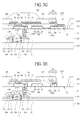
- FIGs. 3A to 3J are cross sectional views illustrating a method of manufacturing the organic light emitting display device according to one embodiment of the present disclosure, which relate to the organic light emitting display device shown in FIG. 2 .
- the same reference numbers will be used throughout the drawings to refer to the same or like parts, and a detailed description for the same parts will be omitted.
- a thin film transistor layer (T) including an active layer 110, a gate insulating film 120, a gate electrode 130, an insulating interlayer 140, a source electrode 150 and a drain electrode 160 is provided on a substrate 100.
- the active layer 110 is provided on the substrate 100, the gate insulating film 120 is provided on the active layer 110, the gate electrode 130 is provided on the gate insulating film 120, the insulating interlayer 140 is provided on the gate electrode 130, a first contact hole (CH1) and a second contact hole (CH2) are provided in the gate insulating film 120 and the insulating interlayer 140, the drain electrode 160 which is connected with one end portion of the active layer 110 via the first contact hole (CH1) is provided and the source electrode 150 which is connected with the other end portion of the active layer 110 via the second contact hole (CH2) is provided.
- CH1 first contact hole
- CH2 second contact hole
- the source electrode 150 includes a lower source electrode 151 and an upper source electrode 152.
- the drain electrode 160 includes a lower drain electrode 161 and an upper drain electrode 162.
- the source electrode 150 and the drain electrode 160 may be simultaneously patterned by the same material for the same process.
- a passivation layer 165 is provided on the source electrode 150 and the drain electrode 160, and a first planarization layer 171 is provided on the passivation layer 165.
- the passivation layer 165 and the first planarization layer 171 are provided to include a third contact hole (CH3), wherein the source electrode 150 is exposed to the outside via the third contact hole (CH3).
- a first anode electrode 180, an auxiliary electrode 190 and a contact electrode 190a are provided on the first planarization layer 171.
- the first anode electrode 180 is connected with the source electrode 150 via the third contact hole (CH3).
- the first anode electrode 180 may include a first lower anode electrode 181, a first upper anode electrode 182 and a first cover anode electrode 183.
- the auxiliary electrode 190 is horizontally spaced apart from the first anode electrode 180, and is connected with the contact electrode 190a.
- the auxiliary electrode 190 may include a lower auxiliary electrode 191, an upper auxiliary electrode 192 and a cover auxiliary electrode 193.
- the contact electrode 190a is connected with the auxiliary electrode 190.
- the contact electrode 190a may include a lower contact electrode 191 a (also referred to as a first contact electrode), an upper contact electrode 192a (also referred to as a third contact electrode) and a cover contact electrode 193a (also referred to as a second contact electrode).
- the lower contact electrode 191a and the lower auxiliary electrode 191 are connected with each other, and are formed as one body.
- the cover contact electrode 193a and the cover auxiliary electrode 193 are connected with each other, and are formed as one body.
- the upper contact electrode 192a is spaced apart from the upper auxiliary electrode 192.
- an end (B) of the lower contact electrode 191a may extend more than an end (A) of the cover contact electrode 193a, whereby one predetermined portion of the upper contact electrode 192a may be exposed.
- the upper contact electrode 192a may be removed by the etching process of FIG. 3H , and the hollow space (C) may be prepared in the region from which the upper contact electrode 192a is removed.
- the first anode electrode 180, the auxiliary electrode 190 and the contact electrode 190a may be simultaneously formed by the various patterning processes, whereby there is no need for the additional process.
- a first ITO layer is deposited on the entire surface of the first planarization layer 171; the first upper anode electrode 182, the upper auxiliary electrode 192 and the upper contact electrode 192a are patterned thereon; a second ITO layer is deposited on the entire surface thereof; and then first ITO layer and the second ITO layer are simultaneously patterned so as to form the first lower anode electrode 181, the lower auxiliary electrode 191 and the lower contact electrode 191a of the first ITO layer, and also to form the first cover anode electrode 183, the cover auxiliary electrode 193 and the cover contact electrode 193a of the second ITO layer.
- first lower anode electrode 181, the lower auxiliary electrode 191 and the lower contact electrode 191a may be patterned on the first planarization layer 171; the first upper anode electrode 182, the upper auxiliary electrode 192 and the upper contact electrode 192a may be patterned thereon; and then the first cover anode electrode 183, the cover auxiliary electrode 193 and the cover contact electrode 193a may be patterned thereon.
- the second planarization layer 172 is provided on the first anode electrode 180, the auxiliary electrode 190 and the contact electrode 190a.
- the second planarization layer 172 is provided to include the fourth contact hole (CH4) and the fifth contact hole (CH5).
- the first anode electrode 180 is exposed to the outside via the fourth contact hole (CH4), and the contact electrode 190a is exposed to the outside via the fifth contact hole (CH5).
- the second anode electrode 200 and the protection electrode 210 are provided on the second planarization layer 172.
- the second anode electrode 200 is connected with the first anode electrode 180 via the fourth contact hole (CH4), and the protection electrode 210 is connected with the contact electrode 190a via the fifth contact hole (CH5).
- the protection electrode 210 is spaced apart from the second anode electrode 200.
- the second anode electrode 200 covers all portions of the fourth contact hole (CH4). However, all portions of the fifth contact hole (CH5) are not covered by the protection electrode 210, that is, the predetermined portion of the fifth contact hole (CH5) is exposed to the outside. According to the predetermined portion of the fifth contact hole (CH5) is exposed, the bank 220 to the left of the contact hole CH5 extends to the exposed fifth contact hole (CH5) for the following process of FIG. 3F .
- the second anode electrode 200 may include a second lower anode electrode 201, a second central anode electrode 202 and a second upper anode electrode 203.
- the protection electrode 210 may include a lower protection electrode 211, a central protection electrode 212 and an upper protection electrode 213.
- the second anode electrode 200 and the protection electrode 210 may be simultaneously patterned by the same material for the same process, whereby there is no need for the additional process.
- the bank 220 to the left of the contact hole CH5 is provided on the second anode electrode 200 and the protection electrode 210.
- the bank 220 to the left of the contact hole CH5 is patterned to expose the upper surface of the second anode electrode 200. Also, the bank 220 to the left of the contact hole CH5 is patterned to expose the predetermined portion of the protection electrode 210 in the fifth contact hole (CH5). In this case, the predetermined portion of the bank 220 to the left of the contact hole CH5 extends to the fifth contact hole (CH5) along the lateral side of the second planarization layer 172.
- a photoresist 300 is patterned on the upper surface of the second anode electrode 200 exposed by the bank 220. Accordingly, the upper surface of the second anode electrode 200 is covered by the photoresist 300 so that it is possible to prevent the second anode electrode 200 from being etched by the process of FIG. 3H .
- the photoresist 300 is not patterned in the fifth contact hole (CH5), whereby the predetermined portion of the protection electrode 210 is exposed to the outside.
- the predetermined portion of the protection electrode 210 which is not covered by the photoresist 300, is removed, and the upper contact electrode 192a is also removed at the same time. Accordingly, it is possible to completely form the contact electrode 190a comprising the lower contact electrode 191 a and the cover contact electrode 193a and to prepare the hollow space (C) between the lower contact electrode 191a and the cover contact electrode 193a. That is, the hollow space (C) is prepared in the region from which the upper contact electrode 192a is removed.
- the indium-tin-oxide (ITO) is crystallized for a high temperature curing process of forming the bank 200 and is changed to crystalline ITO, however, the indium-zinc-oxide (IZO) is not crystallized and remains as amorphous IZO due to a high crystalline temperature.
- ITO indium-tin-oxide
- IZO indium-zinc-oxide
- the lower protection electrode 211 and the upper protection electrode 213 of the amorphous IZO may be etched, however, the lower contact electrode 191 a and the cover contact electrode 193a of the crystalline ITO may remain without being etched. According as only the upper contact electrode 192a is removed by the etching process, the hollow space (C) is prepared between the lower contact electrode 191 a and the cover contact electrode 193a.
- the organic emitting layer 240 is provided on the second anode electrode 200.
- the organic emitting layer 240 may be manufactured by a deposition process using a deposition material with superior straightness, for example, evaporation.
- the organic emitting layer 240 is deposited on the upper surface of the bank 220, and the predetermined portion of the upper surface of the lower contact electrode 191a in the fifth contact hole (CH5).
- the organic emitting layer 240 is not deposited in the hollow space (C). That is, for the deposition process of the organic emitting layer 240, the bank 220 serves as the eaves so that it is possible to prevent the organic emitting layer 240 from being deposited in the hollow space (C). As a result, the organic emitting layer 240 is provided to expose the upper surface of the lower contact electrode 191a positioned in the hollow space (C).
- the cathode electrode 250 is provided on the organic emitting layer 240.
- the cathode electrode 250 formed on the bank 220 located to the right of the contact hole CH5 is connected with the contact electrode 190a in the hollow space (C), the cathode electrode 250 is electrically connected with the auxiliary electrode 190.
- the cathode electrode 240 may be manufactured by a deposition process using a deposition material with inferior straightness, for example sputtering.
- the cathode electrode 250 may be deposited in the hollow space (C).
- the cathode electrode 250 is connected with the lower contact electrode 190a in the hollow space (C).
- the top emission type organic light emitting display device may be changed in various types within a range enabling the technical properties of the present invention.
- a light emission may be made in the entire area of the pixel region, or a light emission may be made only in predetermined portions of the pixel region. That is, if the light emission is made in the entire area of the pixel region, a plurality of pixels for the light emission are arranged in the entire pixel region.
- the aforementioned transistor (T), the first anode electrode 180, the second anode electrode 200, the auxiliary electrode 190, the contact electrode 190a, the protection electrode 210 and the organic emitting layer 240 are not provided in the pixel region where the light emission is not made, but not limited to this structure.
- the cathode electrode 250 is electrically connected with the auxiliary electrode 190 by the additional contact electrode 190a, whereby there is no need for the partition having the reversed tapered structure. Thus, there is no problem relating peel-off or collapse of the partition.
Landscapes
- Engineering & Computer Science (AREA)
- Microelectronics & Electronic Packaging (AREA)
- Physics & Mathematics (AREA)
- Optics & Photonics (AREA)
- Manufacturing & Machinery (AREA)
- Electroluminescent Light Sources (AREA)
Abstract
Description
- This application claims the benefit of
Korean Patent Application No. 10-2015-0123257 filed on August 31, 2015 - Embodiments of the present disclosure relate to an organic light emitting display device, and more particularly, to a top emission type organic light emitting display device, and a method of manufacturing the same.
- An organic light emitting display (OLED) device, which is a self light emitting display device, has advantages of low power consumption, rapid response speed, high emission efficiency, high luminance and wide viewing angle.
- According to a direction of light emitted from an organic light emitting device, the OLED device may be largely classified into a top emission type and a bottom emission type. In case of the bottom emission type, a circuit device is disposed between an emitting layer and an image displaying surface, whereby an aperture ratio may be lowered due to the circuit device. Meanwhile, in case of the top emission type, a circuit device is not disposed between an emitting layer and an image displaying surface, whereby an aperture ratio may be improved.
-
FIG. 1 is a cross sectional view of a related art top emission type OLED device. - As shown in
FIG. 1 , a thin film transistor layer (T) including anactive layer 11, agate insulating film 12, agate electrode 13, aninsulating interlayer 14, asource electrode 15, and adrain electrode 16 is provided on asubstrate 10, and then apassivation layer 20 and aplanarization layer 30 are sequentially provided on the thin film transistor layer (T). - Also, an
anode electrode 40 and anauxiliary electrode 50 are provided on theplanarization layer 30. Theauxiliary electrode 50 is provided to reduce a resistance of acathode electrode 80 to be explained later. - On the
anode electrode 40 and theauxiliary electrode 50, abank 60 is provided to define a pixel region. Also, anorganic emitting layer 70 is provided in the pixel region defined by thebank 60, and thecathode electrode 80 is provided on theorganic emitting layer 70. - In case of the top emission type, a light emitted from the
organic emitting layer 70 passes through thecathode electrode 80. In this reason, thecathode electrode 80 is formed of a transparent conductive material, which causes the increase of resistance therein. In order to reduce the resistance of thecathode electrode 80, thecathode electrode 80 is connected with theauxiliary electrode 50. - In order to connect the
cathode electrode 80 with theauxiliary electrode 50, an upper surface of theauxiliary electrode 50 is not covered by theorganic emitting layer 70. That is, after forming theorganic emitting layer 70, the upper surface of theauxiliary electrode 50 is exposed so that thecathode electrode 80 is connected with the upper surface of theauxiliary electrode 50. In order to prevent the upper surface of theauxiliary electrode 50 from being covered by theorganic emitting layer 70, apartition 65 with a reversed tapered structure is provided in the upper surface of theauxiliary electrode 50. - Owing to the
partition 65 with the reversed tapered structure, a space is provided between thebank 60 and thepartition 65. In this case, thepartition 65 with the reversed tapered structure serves as eaves, whereby theorganic emitting layer 70 is not deposited in the space. That is, theorganic emitting layer 70 may be manufactured by a deposition process using a deposition material with superior straightness, for example, evaporation. Thus, for the deposition process of theorganic emitting layer 70, thepartition 65 serves as the eaves so that it is possible to prevent theorganic emitting layer 70 from being deposited in the space between thebank 60 and thepartition 65. - Meanwhile, the
cathode electrode 80 may be manufactured by a deposition process using a deposition material with inferior straightness, for example, sputtering. Thus, for the deposition process of thecathode electrode 80, thecathode electrode 80 may be deposited in the space between thebank 60 and thepartition 65 so that thecathode electrode 80 may be electrically connected with theauxiliary electrode 50. - However, since the related art top emission type organic light emitting display device necessarily includes the
partition 65 with the reversed tapered structure, it may have the following problems. - In order to pattern the
partition 65 with the reversed tapered structure, it is necessary to carry out a PEB (Post Exposure Bake) process. However, it is difficult to control the PEB process to obtain the desired reversed tapered structure. If the desired reversed tapered structure is not created, thepartition 65 may collapse or peel off. In this case, an electrical connection between thecathode electrode 80 and theauxiliary electrode 50 may be difficult. - Accordingly, embodiments of the present disclosure are directed to a top emission type organic light emitting display device that substantially obviates one or more problems due to limitations and disadvantages of the related art.
- An aspect of the present disclosure is directed to provide a top emission type organic light emitting display device which facilitates an electrical connection between a cathode electrode and an auxiliary electrode without a partition having a reversed tapered structure.
- Additional advantages and features of embodiments of the disclosure will be set forth in part in the description which follows and in part will become apparent to those having ordinary skill in the art upon examination of the following or may be learned from practice of embodiments of the invention. The objectives and other advantages of embodiments of the invention may be realized and attained by the structure particularly pointed out in the written description and claims hereof as well as the appended drawings.
- To achieve these and other advantages, there is provided an organic light emitting display device that may include an anode electrode on a substrate; an organic emitting layer on the anode electrode; a cathode electrode on the organic emitting layer; an auxiliary electrode electrically connected with the cathode electrode; and a contact electrode that is on a same layer as the auxiliary electrode, the contact electrode horizontally spaced apart from the auxiliary electrode, the contact electrode directly connected with both the auxiliary electrode and the cathode electrode to connect together the auxiliary electrode and a portion of the cathode electrode that is on a same layer as the auxiliary electrode..
- In another aspect of the present disclosure, there is provided a method of manufacturing an organic light emitting display device that may include forming a contact electrode over a substrate, the contact electrode including a first contact electrode, a second contact electrode on the first contact electrode, and a third contact electrode on the second contact electrode, the first contact electrode formed with an end that horizontally extends past an end of the third contact electrode; forming a planarization layer over the contact electrode, the planarization layer including a contact hole that exposes the contact electrode; forming a protection electrode on the planarization layer, the protection electrode connected to the contact electrode via the contact hole in the planarization layer; forming a bank that overlaps a portion of the protection electrode, a portion of the first contact electrode, a portion of the second contact electrode, and the end of the third contact electrode; etching a portion of the protection electrode and a portion of the second contact electrode that are not overlapped by the bank to create a hollow space between the portion of the second contact electrode and the portion of the first contact electrode that are overlapped by the bank; and forming a cathode electrode which extends to the hollow space and is connected to the first contact electrode at the hollow space.
- There is provided an organic light emitting display device comprises: an anode electrode on a substrate; an organic emitting layer on the anode electrode; a cathode electrode on the organic emitting layer; an auxiliary electrode electrically connected with the cathode electrode; and a contact electrode that is on a same layer as the auxiliary electrode, the contact electrode horizontally spaced apart from the auxiliary electrode, the contact electrode directly connected with both the auxiliary electrode and the cathode electrode to connect together the auxiliary electrode and a portion of the cathode electrode that is on a same layer as the auxiliary electrode.
- The contact electrode may include a first contact electrode and a second contact electrode that is positioned over the first contact electrode.
- The second contact electrode may include a step-shaped portion that overlaps a portion of the first contact electrode, the step-shaped portion of the second contact electrode and the overlapped portion of the first contact electrode forming a hollow space between the step-shaped portion of the second electrode and the overlapped portion of the first contact electrode.
- A portion of the cathode electrode may extend to the hollow space in the layer including the auxiliary electrode and the contact electrode, and the cathode electrode may directly connect to the first contact electrode.
- The step-shaped portion may include a vertical portion and a horizontal portion connected to the vertical portion, the horizontal portion substantially parallel with the substrate.
- An end of the first contact electrode may horizontally extend past an end of the second contact electrode in a direction away from the auxiliary electrode.
- The auxiliary electrode may further comprise: a first auxiliary electrode; a second auxiliary electrode on the first auxiliary electrode; and a third auxiliary electrode on the second auxiliary electrode, wherein the first auxiliary electrode is connected to the first contact electrode, and the third auxiliary electrode is connected to the second contact electrode.
- A thickness of the second auxiliary electrode may be greater than thicknesses of the first auxiliary electrode and the third auxiliary electrode, the first auxiliary electrode and the third auxiliary electrode may have a higher resistance to corrosion than the second auxiliary electrode, and the third auxiliary electrode may cover an upper surface and side surfaces of the second auxiliary electrode.
- The organic light emitting display device may further comprise a protection electrode positioned on the second contact electrode, wherein an end of the first contact electrode horizontally extends past an end of the protection electrode.
- The protection electrode may comprise: a first protection electrode; a second protection electrode on the first protection electrode; and a third protection electrode on the second protection electrode, wherein the first protection electrode and the third protection electrode have a higher resistance to corrosion than the second protection electrode, and wherein a thickness of the second protection electrode is greater than thicknesses of the first protection electrode and the third protection electrode.
- The anode electrode may comprise: a first anode electrode, wherein a portion of the first anode electrode is in a same layer as the auxiliary electrode and the contact electrode; and a second anode electrode over the first anode electrode, the second anode electrode directly connected with the first anode electrode via a contact hole.
- Each of the first anode electrode and the second anode electrode may comprise: a first anode electrode portion; a second anode electrode portion on the first anode electrode portion; and a third anode electrode portion on the second anode electrode portion, wherein the first anode electrode portion and the third anode electrode portion have a higher resistance to corrosion than the second anode electrode portion; and wherein a thickness of the second anode electrode portion is greater than thicknesses of the first anode electrode portion and the third anode electrode portion.
- The organic light emitting display device may further comprise a planarization layer over the auxiliary electrode, and the contact electrode, the planarization layer including a contact hole that exposes the contact electrode, wherein the contact hole extends to the hollow space formed between the step-shaped portion of the second electrode and the overlapped portion of the first contact electrode.
- The organic light emitting display device may further comprise: a bank over the hollow space and on the planarization layer.
- The contact electrode may be made of a material that is resistance to etchant compared to a material of the protection electrode.
- There is also provided a method of manufacturing an organic light emitting display device comprises: forming a contact electrode over a substrate, the contact electrode including a first contact electrode, a second contact electrode on the first contact electrode, and a third contact electrode on the second contact electrode, the first contact electrode formed with an end that horizontally extends past an end of the third contact electrode; forming a planarization layer over the contact electrode, the planarization layer including a contact hole that exposes the contact electrode; forming a protection electrode on the planarization layer, the protection electrode connected to the contact electrode via the contact hole in the planarization layer; forming a bank that overlaps a portion of the protection electrode, a portion of the first contact electrode, a portion of the second contact electrode, and the end of the third contact electrode; etching a portion of the protection electrode and a portion of the second contact electrode that are not overlapped by the bank to create a hollow space between the portion of the third contact electrode and the portion of the first contact electrode that are overlapped by the bank; and forming a cathode electrode which extends to the hollow space and is connected to the first contact electrode at the hollow space.
- The method may further comprise: simultaneously forming an auxiliary electrode that is connected with the contact electrode and a first anode electrode in a same layer, the auxiliary electrode horizontally spaced apart from the first anode electrode, wherein the contact electrode is simultaneously formed with the auxiliary electrode and the first anode electrode.
- The method may further comprise: forming a second anode electrode that is connected with the first anode electrode, wherein a portion of the second anode electrode is formed in a different layer than the first anode electrode, wherein the second anode electrode and the protection electrode are simultaneously formed in a same layer.
- The method may further comprise: covering the second anode electrode with a mask before etching the portion of the protection electrode and the portion of the second contact electrode that is not overlapped by the bank.
- Etching may comprise: using an etchant to simultaneously remove the portion of the protection electrode and the portion of the second contact electrode that are not overlapped by the bank.
- It is to be understood that both the foregoing general description and the following detailed description of embodiments of the present invention are exemplary and explanatory and are intended to provide further explanation of the invention as claimed.
- The accompanying drawings, which are included to provide a further understanding of embodiments of the invention and are incorporated in and constitute a part of this application, illustrate embodiment(s) of the present disclosure and together with the description serve to explain the principle of embodiments of the invention. In the drawings:
-
FIG. 1 is a cross sectional view illustrating a related art top emission type organic light emitting display device; -
FIG. 2 is a cross sectional view illustrating an organic light emitting display device according to one embodiment of the present disclosure; and -
FIGs. 3A to 3J are cross sectional views illustrating a method of manufacturing the organic light emitting display device according to one embodiment of the present disclosure. - Reference will now be made in detail to the exemplary embodiments of the present invention, examples of which are illustrated in the accompanying drawings. Wherever possible, the same reference numbers will be used throughout the drawings to refer to the same or like parts.
- Advantages and features of the present invention, and implementation methods thereof will be clarified through following embodiments described with reference to the accompanying drawings. The present invention may, however, be embodied in different forms and should not be construed as limited to the embodiments set forth herein. Rather, these embodiments are provided so that this disclosure will be thorough and complete, and will fully convey the scope of the present invention to those skilled in the art. Further, the present invention is only defined by scopes of claims.
- A shape, a size, a ratio, an angle, and a number disclosed in the drawings for describing embodiments of the present invention are merely an example, and thus, the present invention is not limited to the illustrated details. Like reference numerals refer to like elements throughout. In the following description, when the detailed description of the relevant known function or configuration is determined to unnecessarily obscure the important point of the present invention, the detailed description will be omitted. In a case where 'comprise', 'have', and 'include' described in the present specification are used, another part may be added unless 'only-' is used. The terms of a singular form may include plural forms unless referred to the contrary. In construing an element, the element is construed as including an error region although there is no explicit description.
- In description of embodiments of the present disclosure, when a structure (for example, an electrode, a line, a wiring, a layer, or a contact) is described as being formed at an upper portion/lower portion of another structure or on/under the other structure, this description should be construed as including a case where the structures contact each other and moreover, a case where a third structure is disposed there between.
- In describing a time relationship, for example, when the temporal order is described as 'after-', 'subsequent-', 'next-', and 'before-', a case which is not continuous may be included unless 'just' or 'direct' is used.
- It will be understood that, although the terms "first", "second", etc. may be used herein to describe various elements, these elements should not be limited by these terms. These terms are only used to distinguish one element from another. For example, a first element could be termed a second element, and, similarly, a second element could be termed a first element, without departing from the scope of the present invention.
- Features of various embodiments of the present invention may be partially or overall coupled to or combined with each other, and may be variously inter-operated with each other and driven technically as those skilled in the art can sufficiently understand. The embodiments of the present invention may be carried out independently from each other, or may be carried out together in co-dependent relationship.
- Hereinafter, an organic light emitting display device according to embodiments of the present invention will be described in detail with reference to the accompanying drawings.
-
FIG. 2 is a cross sectional view illustrating an organic light emitting display device according to one embodiment of the present disclosure. - As shown in
FIG. 2 , the organic light emitting display device according to one embodiment of the present disclosure may include asubstrate 100, a thin film transistor layer (T), apassivation layer 165, afirst planarization layer 171, asecond planarization layer 172, afirst anode electrode 180, asecond anode electrode 200, anauxiliary electrode 190, acontact electrode 190a, aprotection electrode 210, abank 220, an organic emittinglayer 240 and acathode electrode 250. - The
substrate 100 may be formed of glass or transparent plastic. - The thin film transistor layer (T) may include an
active layer 110, agate insulating film 120, agate electrode 130, an insulatinginterlayer 140, asource electrode 150 and adrain electrode 160. - The
active layer 110 is provided on thesubstrate 100, wherein theactive layer 110 overlaps with thegate electrode 130. Theactive layer 110 may be formed of a silicon-based semiconductor material or oxide-based semiconductor material. Although not shown, a light shielding layer may be additionally provided between thesubstrate 100 and theactive layer 110. In this case, an external light, which is incident on a lower surface of thesubstrate 100, is blocked by the light shielding layer so that it is possible to prevent theactive layer 110 from being damaged by the external light. - The
gate insulating film 120 is provided on theactive layer 110. Thegate insulating film 120 insulates theactive layer 110 and thegate electrode 130 from each other. For example, thegate insulating film 120 may be formed of an inorganic insulating material, and more particularly, thegate insulating film 120 may be formed in a single-layered structure of the inorganic insulating material such as silicon oxide SiOx or silicon nitride SiNx, or a multi-layered structure of the above silicon oxide SiOx and silicon nitride SiNx, but not limited to these structures. - The
gate electrode 130 is provided on thegate insulating film 120. Thegate electrode 130 overlaps with theactive layer 110, and thegate insulating film 120 is interposed between thegate electrode 130 and theactive layer 110 being overlapped with each other. Thegate electrode 130 may be formed in a single-layered structure or multi-layered structure including molybdenum (Mo), aluminum (Al), chrome or chromium (Cr), aurum or gold (Au), titanium (Ti), nickel (Ni), neodymium (Nd), copper (Cu) and their alloys, but not limited to these materials. - The insulating
interlayer 140 is provided on thegate electrode 130. The insulatinginterlayer 140 is formed of the same material as that of thegate insulating film 120. For example, the insulatinginterlayer 140 may be formed in a single-layered structure of the inorganic insulating material such as silicon oxide SiOx or silicon nitride SiNx, or a multi-layered structure of the above silicon oxide SiOx, silicon nitride SiNx and their alloys, but not limited to these materials. - The
source electrode 150 and thedrain electrode 160 confronting each other are provided on the insulatinginterlayer 140. A first contact hole (CH1) for exposing one end portion of theactive layer 110 is provided in the aforementionedgate insulating film 120 and the insulatinginterlayer 140, and a second contact hole (CH2) for exposing the other end portion of theactive layer 110 is provided in the aforementionedgate insulating film 120 and the insulatinginterlayer 140. Thesource electrode 150 is connected with the other end portion of theactive layer 110 via the second contact hole (CH2), and thedrain electrode 160 is connected with one end portion of theactive layer 110 via the first contact hole (CH1). - The
source electrode 150 may include alower source electrode 151 and anupper source electrode 152. - The
lower source electrode 151 is provided between the insulatinginterlayer 140 and theupper source electrode 152, wherein thelower source electrode 151 enhances an adhesive strength between the insulatinginterlayer 140 and theupper source electrode 152. Also, thelower source electrode 151 protects a lower surface of theupper source electrode 152 so that it is possible to prevent the lower surface of the upper source electrode 152 from being corroded. Thus, an oxidation degree of thelower source electrode 151 may be lower than an oxidation degree of theupper source electrode 152. That is, a corrosion resistance in a material of thelower source electrode 151 may be superior to a corrosion resistance in a material of theupper source electrode 152. Thelower source electrode 151 functions as an adhesion enhancement layer or a corrosion preventing layer. Thelower source electrode 151 may be formed of an alloy MoTi of molybdenum and titanium, but not limited to this material. - The
upper source electrode 152 is provided on an upper surface of thelower source electrode 151. Theupper source electrode 152 may be formed of a low-resistance metal material such as copper Cu, but not limited to this metal material. Theupper source electrode 152 may be formed of a metal material whose resistance is relatively lower than that of thelower source electrode 151. In order to lower a total resistance of thesource electrode 150, a thickness of theupper source electrode 152 may be larger than a thickness of thelower source electrode 151, preferably. - In the same way as the
aforementioned source electrode 150, thedrain electrode 160 may include alower drain electrode 161 and anupper drain electrode 162. - The
lower drain electrode 161 is provided between the insulatinginterlayer 140 and theupper drain electrode 162, wherein thelower drain electrode 161 enhances an adhesive strength between the insulatinginterlayer 140 and theupper drain electrode 162. Also, thelower drain electrode 161 prevents a lower surface of theupper drain electrode 162 from being corroded. Thus, an oxidation degree of thelower drain electrode 161 may be lower than an oxidation degree of theupper drain electrode 162. That is, a corrosion resistance in a material of thelower drain electrode 161 may be superior to a corrosion resistance in a material of theupper drain electrode 162. Thelower drain electrode 161 may be formed of an alloy MoTi of molybdenum and titanium, but not limited to this material. - The
upper drain electrode 162 is provided on an upper surface of thelower drain electrode 161. Theupper drain electrode 162 may be formed of the same material as that of the aforementionedupper source electrode 152, for example, copper Cu, but not limited to this material. In order to lower a total resistance of thedrain electrode 160, a thickness of theupper drain electrode 162 may be larger than a thickness of thelower drain electrode 161, preferably. - The
upper drain electrode 162 may be formed of the same material as that of theupper source electrode 152, and theupper drain electrode 162 may be formed in the same thickness as that of theupper source electrode 152. Thelower drain electrode 161 may be formed of the same material as that of thelower source electrode 151, and thelower drain electrode 161 may be formed in the same thickness as that of thelower source electrode 151. In this case, thedrain electrode 160 and thesource electrode 150 may be simultaneously manufactured in the same process. - A structure of the thin film transistor layer (T) is not limited to the above structure, that is, a structure of the thin film transistor layer (T) may be changed to various shapes generally known to those in the art. For example, the drawing shows a top gate structure where the
gate electrode 130 is provided on theactive layer 110, but not necessarily. That is, it is possible to provide a bottom gate structure where thegate electrode 130 is provided below theactive layer 110. - The
passivation layer 165 is provided on the thin film transistor layer (T), and more particularly, on upper surfaces of thesource electrode 150 and thedrain electrode 160. Thepassivation layer 165 protects the thin film transistor layer (T). Thepassivation layer 165 may be formed of an inorganic insulating material, for example, silicon oxide film SiOx or silicon nitride film SiNx, but not limited to these materials. - The
first planarization layer 171 is provided on thepassivation layer 165. Thefirst planarization layer 171 is provided to planarize an upper surface of thesubstrate 100 with the thin film transistor layer (T). Thefirst planarization layer 171 may be formed of an organic insulating material, for example, acryl resin, epoxy resin, phenolic resin, polyamide resin, polyimide resin, and etc., but not limited to these materials. - The
first anode electrode 180 and theauxiliary electrode 190 are provided on thefirst planarization layer 171. That is, thefirst anode electrode 180 and theauxiliary electrode 190 are disposed in the same layer. A third contact hole (CH3) for exposing thesource electrode 150 is provided in theaforementioned passivation layer 165 and thefirst planarization layer 171. Thesource electrode 150 and thefirst anode electrode 180 are connected with each other via the third contact hole (CH3). - The
first anode electrode 180 may include a first lower anode electrode 181 (a first anode electrode portion of the first anode electrode), a first upper anode electrode 182 (a second anode electrode portion of the first anode electrode) and a first cover anode electrode 183 (a third anode electrode portion of the first anode electrode). - The first
lower anode electrode 181 is provided between thefirst planarization layer 171 and the firstupper anode electrode 182, wherein the firstlower anode electrode 181 enhances an adhesive strength between thefirst planarization layer 171 and the firstupper anode electrode 182. Also, the firstlower anode electrode 181 protects a lower surface of the firstupper anode electrode 182 so that it is possible to prevent the lower surface of the firstupper anode electrode 182 from being corroded. Thus, an oxidation degree of the firstlower anode electrode 181 may be lower than an oxidation degree of the firstupper anode electrode 182. That is, a corrosion resistance in a material of the firstlower anode electrode 181 may be superior to a corrosion resistance in a material of the firstupper anode electrode 182. Also, the firstlower anode electrode 181 protects an upper surface of theupper source electrode 152 so that it is possible to prevent the upper surface of the upper source electrode 152 from being corroded. Thus, an oxidation degree of the firstlower anode electrode 181 may be lower than an oxidation degree of theupper source electrode 152. That is, a corrosion resistance in a material of the firstlower anode electrode 181 may be superior to a corrosion resistance in a material of theupper source electrode 152. The firstlower anode electrode 181 prevents the upper surface of the upper source electrode 152 from being corroded so that it is possible to provide the aforementioned dual-layered structure in thesource electrode 150. The firstlower anode electrode 181 functions as an adhesion enhancement layer or a corrosion preventing layer. The firstlower anode electrode 181 may be formed of indium-tin-oxide (ITO), but not limited to this material. - The first
upper anode electrode 182 is provided between the firstlower anode electrode 181 and the firstcover anode electrode 183. The firstupper anode electrode 182 may be formed of a low-resistance metal material such as copper Cu, but not limited to this metal material. The firstupper anode electrode 182 may be formed of a metal material whose resistance is relatively lower than that in each of the firstlower anode electrode 181 and the firstcover anode electrode 183. In order to lower a total resistance of thefirst anode electrode 180, a thickness of the firstupper anode electrode 182 may be larger than a thickness in each of the firstlower anode electrode 181 and the firstcover anode electrode 183, preferably. - The first
cover anode electrode 183 is provided on the firstupper anode electrode 182. The firstcover anode electrode 183 covers upper and lateral surfaces of the firstupper anode electrode 182 so that the firstcover anode electrode 183 prevents the firstupper anode electrode 182 from being corroded. Thus, an oxidation degree of the firstcover anode electrode 183 may be lower than an oxidation degree of the firstupper anode electrode 182. That is, a corrosion resistance in a material of the firstcover anode electrode 183 may be superior to a corrosion resistance in a material of the firstupper anode electrode 182. The firstcover anode electrode 183 also covers lateral surfaces of the firstlower anode electrode 181. The firstcover anode electrode 183 may be formed of a transparent conductive material such as indium-tin-oxide (ITO), but not limited to this material. - The
auxiliary electrode 190 is spaced apart from thefirst anode electrode 180. In the same way as the aforementionedfirst anode electrode 180, theauxiliary electrode 190 may include a lower auxiliary electrode 191 (also referred to as a first auxiliary electrode), an upper auxiliary electrode 192 (also referred to as a second auxiliary electrode) and a cover auxiliary electrode 193 (also referred to as a third auxiliary electrode). - The lower
auxiliary electrode 191 is provided between thefirst planarization layer 171 and the upperauxiliary electrode 192, wherein the lowerauxiliary electrode 191 enhances an adhesive strength between thefirst planarization layer 171 and the upperauxiliary electrode 192, and also prevents a lower surface of the upperauxiliary electrode 192 from being corroded. Thus, an oxidation degree of the lowerauxiliary electrode 191 may be lower than an oxidation degree of the upperauxiliary electrode 192. That is, a corrosion resistance in a material of the lowerauxiliary electrode 191 may be superior to a corrosion resistance in a material of the upperauxiliary electrode 192. The lowerauxiliary electrode 191 may be formed of the same material as that of the aforementioned firstlower anode electrode 181, that is, indium-tin-oxide (ITO), but not limited to this material. - The upper
auxiliary electrode 192 is provided between the lowerauxiliary electrode 191 and the coverauxiliary electrode 193. The upperauxiliary electrode 192 may be formed of the same material as that of the aforementioned firstupper anode electrode 182, that is, copper Cu, but not limited to this material. In order to lower a total resistance of theauxiliary electrode 190, a thickness of the upperauxiliary electrode 192 with a relatively low resistance may be larger than a thickness of each of the lowerauxiliary electrode 191 and the coverauxiliary electrode 193 with a relatively high resistance, preferably. - The cover
auxiliary electrode 193 is provided on the upperauxiliary electrode 192. The coverauxiliary electrode 193 covers upper and lateral (e.g., side) surfaces of the upperauxiliary electrode 192 so that the coverauxiliary electrode 193 prevents the upperauxiliary electrode 192 from being corroded. Thus, an oxidation degree of the coverauxiliary electrode 193 may be lower than an oxidation degree of the upperauxiliary electrode 192. That is, a corrosion resistance in a material of the coverauxiliary electrode 193 may be superior to a corrosion resistance in a material of the upperauxiliary electrode 192. The coverauxiliary electrode 193 also covers lateral surfaces of the lowerauxiliary electrode 191. The coverauxiliary electrode 193 may be formed of a transparent conductive material such as indium-tin-oxide (ITO), but not limited to this material. - The cover
auxiliary electrode 193 may be formed of the same material as that of the firstcover anode electrode 183, and the coverauxiliary electrode 193 may be formed in the same thickness as that of the firstcover anode electrode 183. The upperauxiliary electrode 192 may be formed of the same material as that of the firstupper anode electrode 182, and the upperauxiliary electrode 192 may be formed in the same thickness as that of the firstupper anode electrode 182. The lowerauxiliary electrode 191 may be formed of the same material as that of the firstlower anode electrode 181, and the lowerauxiliary electrode 191 may be formed in the same thickness as that of the firstlower anode electrode 181. In this case, theauxiliary electrode 190 and thefirst anode electrode 180 may be simultaneously manufactured in the same process. - According to one embodiment of the present disclosure, the
auxiliary electrode 190 is provided in the same layer as thefirst anode electrode 180 instead of thesecond anode electrode 200 so that it is possible to efficiently lower the resistance of thecathode electrode 250 without decreasing a pixel region. In detail, if theauxiliary electrode 190 is formed in the same layer as thesecond anode electrode 200, theauxiliary electrode 190 is increased in size so as to lower the resistance of thecathode electrode 250, and thus thesecond anode electrode 200 is decreased in size, thereby decreasing the pixel region. - Meanwhile, according to one embodiment of the present disclosure, if the
auxiliary electrode 190 is formed in the same layer as thefirst anode electrode 180, theauxiliary electrode 190 is increased in size so as to lower the resistance of thecathode electrode 250. In this case, even though thefirst anode electrode 180 is decreased in size, the pixel region is not decreased. That is, thefirst anode electrode 180 connects thesource electrode 150 and thesecond anode electrode 200 with each other. Thus, even though thefirst anode electrode 180 is decreased in width, the pixel region is not decreased. The pixel region depends on thesecond anode electrode 200. - According to one embodiment of the present disclosure, it is possible to increase a width of the
auxiliary electrode 190 without decreasing the pixel region. In detail, as shown in the drawings, the width of theauxiliary electrode 190 is increased so as to overlap theauxiliary electrode 190 with thesecond anode electrode 200 so that it is possible to efficiently lower the resistance of thecathode electrode 250. - In the same manner as the
first anode electrode 180 and theauxiliary electrode 190, thecontact electrode 190a is provided on thefirst planarization layer 171. That is, thecontact electrode 190a is provided in the same layer as thefirst anode electrode 180 and theauxiliary electrode 190. - The
contact electrode 190a connects theauxiliary electrode 190 with thecathode electrode 250. Thus, thecontact electrode 190a is electrically connected with theauxiliary electrode 190, and is also electrically connected with thecathode electrode 250. Especially, thecontact electrode 190a is directly connected with theauxiliary electrode 190 and thecathode electrode 250. - The
contact electrode 190a may include alower contact electrode 191a and acover contact electrode 193a. - The
lower contact electrode 191a is provided on thefirst planarization layer 171. Thelower contact electrode 191a is directly connected with the lowerauxiliary electrode 191. Especially, thelower contact electrode 191 a may be formed of the same material as that of the lowerauxiliary electrode 191, and may be formed in the same thickness as that of the lowerauxiliary electrode 191 as one body. In this case, thelower contact electrode 191 a and the lowerauxiliary electrode 191 may be simultaneously manufactured in the same process. Also, thelower contact electrode 191a may be directly connected with thecathode electrode 250. In more detail, thecathode electrode 250 is brought into contact with the upper surface of thelower contact electrode 191a. - The
cover contact electrode 193a is provided on thelower contact electrode 191a. Thecover contact electrode 193a is connected with thelower contact electrode 191a, and is also connected with the coverauxiliary electrode 193. Especially, thecover contact electrode 193a may be formed of the same material as that of the coverauxiliary electrode 193, and may be formed in the same thickness as that of the coverauxiliary electrode 193 as one body. In this case, thecover contact electrode 193a and the coverauxiliary electrode 193 may be simultaneously manufactured in the same process. Thecontact electrode 190a and theauxiliary electrode 190 may be horizontally spaced apart from each other are connected to each other via anintermediate electrode 170. Theintermediate electrode 170 includes a firstintermediate electrode 170a and a secondintermediate electrode 170b. The firstintermediate electrode 170a is directly connected to thelower contact electrode 191a and the lowerauxiliary electrode 191. The secondintermediate electrode 170b is directly connected to thecover contact electrode 193a and the coverauxiliary electrode 193. - An end (A) of the
cover contact electrode 193a, which does not confront theauxiliary electrode 190, is provided at a predetermined interval from an end (B) of thelower contact electrode 191a which does not confront theauxiliary electrode 190, whereby a hollow space (C) is prepared between thecover contact electrode 193a and thelower contact electrode 191a. In the hollow space (C), thelower contact electrode 191a and thecathode electrode 250 are connected with each other. In order to prepare the hollow space (C), the end (B) of thelower contact electrode 191a extends more than the end (A) of thecover contact electrode 193a, preferably. This is for an easy permeation of an etchant into the space between thecover contact electrode 193a and thelower contact electrode 191a for the following process ofFIG. 3H to be explained later. - The
lower contact electrode 191a and thecover contact electrode 193a may be formed of a material which is not etched by an etchant capable of etching a material for the upperauxiliary electrode 192, for example, crystalline indium-tin-oxide (ITO). - The
second planarization layer 172 is provided on thefirst anode electrode 180, theauxiliary electrode 190 and thecontact electrode 190a. Thesecond planarization layer 172 together with the aforementionedfirst planarization layer 171 planarizes the upper surface of thesubstrate 100. Thesecond planarization layer 172 may be formed of an organic insulating material, for example, acryl resin, epoxy resin, phenolic resin, polyamide resin, polyimide resin, and etc., but not limited to these materials. - A fourth contact hole (CH4) and a fifth contact hole (CH5) are provided in the
second planarization layer 172. Thefirst anode electrode 180 is exposed via the fourth contact hole (CH4), and thecontact electrode 190a is exposed via the fifth contact hole (CH5). The fifth contact hole (CH5) is in contact with the hollow space (C), whereby thecathode electrode 250 may extend to the hollow space (C) via the fifth contact hole (CH5), and thus thecathode electrode 250 may be connected with thecontact electrode 190a in the hollow space (C). - The
second anode electrode 200 is provided on thesecond planarization layer 172. Thesecond anode electrode 200 is connected with thefirst anode electrode 180 via the fourth contact hole (CH4). Thesecond anode electrode 200 reflects a light emitted from the organic emittinglayer 240 to an upper direction. In this reason, thesecond anode electrode 200 includes a material with good reflectance. Thesecond anode electrode 200 may include a second lower anode electrode 201 (a first anode electrode portion of the second anode electrode), a second central anode electrode 202 (a second anode electrode portion of the second anode electrode) and a second upper anode electrode 203 (a third anode electrode portion of the second anode electrode). - The second
lower anode electrode 201 is provided between thefirst anode electrode 180 and the secondcentral anode electrode 202. The secondlower anode electrode 201 protects a lower surface of the secondcentral anode electrode 202 so that it is possible to prevent the lower surface of the secondcentral anode electrode 202 from being corroded. Thus, an oxidation degree of the secondlower anode electrode 201 may be lower than an oxidation degree of the secondcentral anode electrode 202. That is, a corrosion resistance in a material of the secondlower anode electrode 201 may be superior to a corrosion resistance in a material of the secondcentral anode electrode 202. The secondlower anode electrode 201 may be formed of a transparent conductive material such as indium-tin-oxide (ITO) or indium-zinc-oxide (IZO), but not limited to these materials. - The second
central anode electrode 202 is provided between the secondlower anode electrode 201 and the secondupper anode electrode 203. The secondcentral anode electrode 202 may be formed of a material with relatively-low resistance and relatively-high reflectance in comparison to the secondlower anode electrode 201 and the secondupper anode electrode 203, for example, argentums or silver Ag, but not limited to this material. In order to lower a total resistance of thesecond anode electrode 200, a thickness of the secondcentral anode electrode 202 with relatively-low resistance may be larger than a thickness in each of the secondlower anode electrode 201 and the secondupper anode electrode 203 with relatively-high resistance, preferably. - The second
upper anode electrode 203 is provided on an upper surface of the secondcentral anode electrode 202 so that it is possible to prevent the upper surface of the secondcentral anode electrode 202 from being corroded. Thus, an oxidation degree of the secondupper anode electrode 203 may be lower than an oxidation degree of the secondcentral anode electrode 202. That is, a corrosion resistance in a material of the secondupper anode electrode 203 may be superior to a corrosion resistance in a material of the secondcentral anode electrode 202. The secondupper anode electrode 203 may be formed of a transparent conductive material such as indium-tin-oxide (ITO) or indium-zinc-oxide (IZO), but not limited to this material. - The
protection electrode 210 is spaced apart from thesecond anode electrode 200. Like thesecond anode electrode 200, theprotection electrode 210 is provided on thesecond planarization layer 172. Theprotection electrode 210 protects thecontact electrode 190a. In detail, theprotection electrode 210 is configured to prepare the hollow space (C) between thecover contact electrode 193a and thelower contact electrode 191 a. To this end, the end (B) of thelower contact electrode 191 a extends more than an end (D) of theprotection electrode 210 which does not confront thesecond anode electrode 200, preferably. That is, theprotection electrode 210 remains after the etching process in the process ofFIG. 3H relating the following manufacturing process to be explained later. Thus, the end (B) of thelower contact electrode 191a extends more than the end (D) of theprotection electrode 210, as shown inFIG. 2 . - The
protection electrode 210 is connected with thecontact electrode 190a via the fifth contact hole (CH5) provided in thesecond planarization layer 172. Especially, theprotection electrode 210 is brought into contact with the upper surface of thecover contact electrode 193a. Theprotection electrode 210 is electrically connected with theauxiliary electrode 190 and thecontact electrode 190a so that it is possible to lower the resistance of thecathode electrode 250. - The
protection electrode 210 may include a lower protection electrode 211 (also referred to as a first protection electrode), a central protection electrode 212 (also referred to as a second protection electrode) and an upper protection electrode 213 (also referred to as a third protection electrode). - The
lower protection electrode 211 is provided between thecontact electrode 190a and thecentral protection electrode 212. Thelower protection electrode 211 protects a lower surface of thecentral protection electrode 212 so that thelower protection electrode 211 prevents the lower surface of thecentral protection electrode 212 from being corroded. Accordingly, an oxidation degree of thelower protection electrode 211 may be lower than an oxidation degree of thecentral protection electrode 212. That is, a corrosion resistance in a material of thelower protection electrode 211 may be superior to a corrosion resistance in a material of thecentral protection electrode 212. Thelower protection electrode 211 may be formed of a transparent conductive material such as indium-tin-oxide (ITO) or indium-zinc-oxide (IZO), but not limited to this material. Preferably, thelower protection electrode 211 is formed of a material which is easily etched by the etchant capable of etching the material for the upperauxiliary electrode 192. Thus, thelower protection electrode 211 is formed of indium-zinc-oxide (IZO) which is higher than a crystallization temperature. This will be easily understood by the following description for the manufacturing process to be explained later. - The
central protection electrode 212 is provided between thelower protection electrode 211 and theupper protection electrode 213. Thecentral protection electrode 212 may be formed of a material with relatively-low resistance and relatively-high reflectance in comparison to thelower protection electrode 211 and theupper protection electrode 213, for example, argentums or silver Ag, but not limited to this material. In order to lower a total resistance of theprotection electrode 210, a thickness of thecentral protection electrode 212 with relatively-low resistance may be larger than a thickness in each of thelower protection electrode 211 and theupper protection electrode 213 with relatively-high resistance, preferably. - The
upper protection electrode 213 is provided on an upper surface of thecentral protection electrode 212 so that it is possible to prevent the upper surface of thecentral protection electrode 212 from being corroded. Thus, an oxidation degree of theupper protection electrode 213 may be lower than an oxidation degree of thecentral protection electrode 212. That is, a corrosion resistance in a material of theupper protection electrode 213 may be superior to a corrosion resistance in a material of thecentral protection electrode 212. Theupper protection electrode 213 may be formed of a transparent conductive material such as indium-tin-oxide (ITO) or indium-zinc-oxide (IZO), but not limited to this material. Like the aforementionedlower protection electrode 211, theupper protection electrode 213 is formed of a material which is easily etched by the etchant capable of etching the material for the upperauxiliary electrode 192, preferably. Thus, theupper protection electrode 213 is formed of indium-zinc-oxide IZO which has high crystallization temperature, preferably. This will be easily understood by the following description for the manufacturing process to be explained later. - The
upper protection electrode 213 may be formed of the same material as that of the secondupper anode electrode 203, and may be formed in the same thickness as that of the secondupper anode electrode 203. Thecentral protection electrode 212 may be formed of the same material as that of the secondcentral anode electrode 202, and may be formed in the same thickness as that of the secondcentral anode electrode 202. Thelower protection electrode 211 may be formed of the same material as that of the secondlower anode electrode 201, and may be formed in the same thickness as that of the secondlower anode electrode 201. In this case, theprotection electrode 210 and thesecond anode electrode 200 may be simultaneously manufactured in the same process. - The
bank 220 is provided on thesecond anode electrode 200 and theprotection electrode 210. - The
bank 220, which exposes the upper surface of thesecond anode electrode 200, is provided on one side and the other side of thesecond anode electrode 200. According as thebank 220 is provided to expose the upper surface of thesecond anode electrode 200, it is possible to secure an image-displaying area. Also, thebank 220 is provided between thesecond anode electrode 200 and theprotection electrode 210 so that thesecond anode electrode 200 and theprotection electrode 210 are insulated from each other by thebank 220. Thebank 220 may be formed of an organic insulating material, for example, polyimide resin, acryl resin, benzocyclobutene BCB, and etc., but not limited to these materials. - The
bank 220 is patterned to cover the upper surface of theprotection electrode 210. Thus, theprotection electrode 210 covered by thebank 220 remains after the etching process. Also, thebank 220 is patterned to expose thecontact electrode 190a, and more particularly, thelower contact electrode 191a. That is, thebank 220 is patterned to expose thelower contact electrode 191a via the aforementioned fifth contact hole (CH5). - A predetermined portion of the
bank 220 extends to the fifth contact hole (CH5) along the lateral side of thesecond planarization layer 172, such that thebank 220 overlaps the protection electrode and theupper contact electrode 193a. If the predetermined portion of thebank 220 extends to the fifth contact hole (CH5), thecathode electrode 250 is easily connected with thelower contact electrode 191a along the upper surface of the extendingbank 220. That is, as shown in the drawings, when the predetermined portion of thebank 220 extends to the fifth contact hole (CH5), the organic emittinglayer 240 and thecathode electrode 250 are sequentially deposited on the upper surface of the extendingbank 220. As a result, thecathode electrode 250 formed on thebank 220 located to the right of the contact hole CH5 is brought into contact with the upper surface of thelower contact electrode 191a which is exposed to the outside without being in contact with thebank 220. If thebank 220 to the left of the contact hole CH5 does not extend to the fifth contact hole (CH5), thecathode electrode 250 extending to the fifth contact hole (CH5) may not connect to thelower contact electrode 191 a. - The organic emitting
layer 240 is provided on thesecond anode electrode 200. The organic emittinglayer 240 may include a hole injecting layer, a hole transporting layer, an emitting layer, an electron transporting layer and an electron injecting layer. A structure of the organic emittinglayer 240 may be changed to various shapes generally known to those in the art. - The organic emitting
layer 240 may extend to the upper surface of thebank 220. Also, the organic emittinglayer 240 may extend to the fifth contact hole (CH5) along the upper surface of thebank 220 extending to the fifth contact hole (CH5), and then come in contact the predetermined portion of the upper surface of thelower contact electrode 191a. However, the organic emittinglayer 240 does not extend into the inside of the hollow space (C) prepared between thecover contact electrode 193a and thelower contact electrode 191 a. That is, the organic emittinglayer 240 is provided to expose the upper surface of thelower contact electrode 191a positioned in the hollow space (C) so that thecathode electrode 250 is connected with thelower contact electrode 191 a exposed in the hollow space (C). - The organic emitting
layer 240 may be manufactured by an evaporation method using a deposition material with superior straightness. Thus, the organic emittinglayer 240 is not deposited in the hollow space (C) since thebank 220 serves as the eaves for the deposition process of the organic emittinglayer 240. - The
cathode electrode 250 is provided on the organic emittinglayer 240. Since thecathode electrode 250 is disposed in a light-emission surface, thecathode electrode 250 is formed of a transparent conductive material. According as thecathode electrode 250 is formed of the transparent conductive material, the resistance of the cathode electrode is increased. In order to lower the resistance of thecathode electrode 250, thecathode electrode 250 is connected with theauxiliary electrode 190 through thecontact electrode 190a. In more detail, thecathode electrode 250 extends to the inside of the hollow space (C), and comes into contact with the upper surface of thelower contact electrode 190a. According to one embodiment of the present disclosure, thecathode electrode 250 is electrically connected with theauxiliary electrode 190 through thelower contact electrode 190a provided with the hollow space (C), whereby there is no need for the related art partition with the reversed-tapered structure. That is, there is no problem relating peel-off or collapse of the partition. - The
cathode electrode 250 may be manufactured by sputtering, that is, a deposition process using a deposition material with inferior straightness. Accordingly, thecathode electrode 250 may be deposited in the hollow space (C) for the deposition process of thecathode electrode 250. - Although not shown, an encapsulation layer may be additionally provided on the
cathode electrode 250 so as to prevent a permeation of moisture. The encapsulation layer may be formed of various materials generally known to those in the art. Also, although not shown, a color filter may be additionally provided on thecathode electrode 250 for each pixel. In this case, a white light may be emitted from the organic emittinglayer 240. -
FIGs. 3A to 3J are cross sectional views illustrating a method of manufacturing the organic light emitting display device according to one embodiment of the present disclosure, which relate to the organic light emitting display device shown inFIG. 2 . Thus, the same reference numbers will be used throughout the drawings to refer to the same or like parts, and a detailed description for the same parts will be omitted. - First, as shown in
FIG. 3A , a thin film transistor layer (T) including anactive layer 110, agate insulating film 120, agate electrode 130, an insulatinginterlayer 140, asource electrode 150 and adrain electrode 160 is provided on asubstrate 100. - In more detail, the
active layer 110 is provided on thesubstrate 100, thegate insulating film 120 is provided on theactive layer 110, thegate electrode 130 is provided on thegate insulating film 120, the insulatinginterlayer 140 is provided on thegate electrode 130, a first contact hole (CH1) and a second contact hole (CH2) are provided in thegate insulating film 120 and the insulatinginterlayer 140, thedrain electrode 160 which is connected with one end portion of theactive layer 110 via the first contact hole (CH1) is provided and thesource electrode 150 which is connected with the other end portion of theactive layer 110 via the second contact hole (CH2) is provided. - The
source electrode 150 includes alower source electrode 151 and anupper source electrode 152. Thedrain electrode 160 includes alower drain electrode 161 and anupper drain electrode 162. Thesource electrode 150 and thedrain electrode 160 may be simultaneously patterned by the same material for the same process. - Then, as shown in
FIG. 3B , apassivation layer 165 is provided on thesource electrode 150 and thedrain electrode 160, and afirst planarization layer 171 is provided on thepassivation layer 165. - The
passivation layer 165 and thefirst planarization layer 171 are provided to include a third contact hole (CH3), wherein thesource electrode 150 is exposed to the outside via the third contact hole (CH3). - Then, as shown in
FIG. 3C , afirst anode electrode 180, anauxiliary electrode 190 and acontact electrode 190a are provided on thefirst planarization layer 171. - The
first anode electrode 180 is connected with thesource electrode 150 via the third contact hole (CH3). Thefirst anode electrode 180 may include a firstlower anode electrode 181, a firstupper anode electrode 182 and a firstcover anode electrode 183. - The
auxiliary electrode 190 is horizontally spaced apart from thefirst anode electrode 180, and is connected with thecontact electrode 190a. Theauxiliary electrode 190 may include a lowerauxiliary electrode 191, an upperauxiliary electrode 192 and a coverauxiliary electrode 193. - The
contact electrode 190a is connected with theauxiliary electrode 190. Thecontact electrode 190a may include alower contact electrode 191 a (also referred to as a first contact electrode), anupper contact electrode 192a (also referred to as a third contact electrode) and acover contact electrode 193a (also referred to as a second contact electrode). - The
lower contact electrode 191a and the lowerauxiliary electrode 191 are connected with each other, and are formed as one body. Thecover contact electrode 193a and the coverauxiliary electrode 193 are connected with each other, and are formed as one body. However, theupper contact electrode 192a is spaced apart from the upperauxiliary electrode 192. - In this case, an end (B) of the
lower contact electrode 191a may extend more than an end (A) of thecover contact electrode 193a, whereby one predetermined portion of theupper contact electrode 192a may be exposed. According as one predetermined portion of theupper contact electrode 192a is exposed, theupper contact electrode 192a may be removed by the etching process ofFIG. 3H , and the hollow space (C) may be prepared in the region from which theupper contact electrode 192a is removed. - The
first anode electrode 180, theauxiliary electrode 190 and thecontact electrode 190a may be simultaneously formed by the various patterning processes, whereby there is no need for the additional process. For example, a first ITO layer is deposited on the entire surface of thefirst planarization layer 171; the firstupper anode electrode 182, the upperauxiliary electrode 192 and theupper contact electrode 192a are patterned thereon; a second ITO layer is deposited on the entire surface thereof; and then first ITO layer and the second ITO layer are simultaneously patterned so as to form the firstlower anode electrode 181, the lowerauxiliary electrode 191 and thelower contact electrode 191a of the first ITO layer, and also to form the firstcover anode electrode 183, the coverauxiliary electrode 193 and thecover contact electrode 193a of the second ITO layer. In another way, the firstlower anode electrode 181, the lowerauxiliary electrode 191 and thelower contact electrode 191a may be patterned on thefirst planarization layer 171; the firstupper anode electrode 182, the upperauxiliary electrode 192 and theupper contact electrode 192a may be patterned thereon; and then the firstcover anode electrode 183, the coverauxiliary electrode 193 and thecover contact electrode 193a may be patterned thereon. - Then, as shown in
FIG. 3D , thesecond planarization layer 172 is provided on thefirst anode electrode 180, theauxiliary electrode 190 and thecontact electrode 190a. - The
second planarization layer 172 is provided to include the fourth contact hole (CH4) and the fifth contact hole (CH5). Thefirst anode electrode 180 is exposed to the outside via the fourth contact hole (CH4), and thecontact electrode 190a is exposed to the outside via the fifth contact hole (CH5). - As shown in
FIG. 3E , thesecond anode electrode 200 and theprotection electrode 210 are provided on thesecond planarization layer 172. - The
second anode electrode 200 is connected with thefirst anode electrode 180 via the fourth contact hole (CH4), and theprotection electrode 210 is connected with thecontact electrode 190a via the fifth contact hole (CH5). Theprotection electrode 210 is spaced apart from thesecond anode electrode 200. - The
second anode electrode 200 covers all portions of the fourth contact hole (CH4). However, all portions of the fifth contact hole (CH5) are not covered by theprotection electrode 210, that is, the predetermined portion of the fifth contact hole (CH5) is exposed to the outside. According to the predetermined portion of the fifth contact hole (CH5) is exposed, thebank 220 to the left of the contact hole CH5 extends to the exposed fifth contact hole (CH5) for the following process ofFIG. 3F . - The
second anode electrode 200 may include a secondlower anode electrode 201, a secondcentral anode electrode 202 and a secondupper anode electrode 203. Theprotection electrode 210 may include alower protection electrode 211, acentral protection electrode 212 and anupper protection electrode 213. - The
second anode electrode 200 and theprotection electrode 210 may be simultaneously patterned by the same material for the same process, whereby there is no need for the additional process. - Then, as shown in
FIG. 3F , thebank 220 to the left of the contact hole CH5 is provided on thesecond anode electrode 200 and theprotection electrode 210. - The
bank 220 to the left of the contact hole CH5 is patterned to expose the upper surface of thesecond anode electrode 200. Also, thebank 220 to the left of the contact hole CH5 is patterned to expose the predetermined portion of theprotection electrode 210 in the fifth contact hole (CH5). In this case, the predetermined portion of thebank 220 to the left of the contact hole CH5 extends to the fifth contact hole (CH5) along the lateral side of thesecond planarization layer 172. - As shown in
FIG. 3G , aphotoresist 300 is patterned on the upper surface of thesecond anode electrode 200 exposed by thebank 220. Accordingly, the upper surface of thesecond anode electrode 200 is covered by thephotoresist 300 so that it is possible to prevent thesecond anode electrode 200 from being etched by the process ofFIG. 3H . However, thephotoresist 300 is not patterned in the fifth contact hole (CH5), whereby the predetermined portion of theprotection electrode 210 is exposed to the outside. - Then, as shown in
FIG. 3H , the predetermined portion of theprotection electrode 210, which is not covered by thephotoresist 300, is removed, and theupper contact electrode 192a is also removed at the same time. Accordingly, it is possible to completely form thecontact electrode 190a comprising thelower contact electrode 191 a and thecover contact electrode 193a and to prepare the hollow space (C) between thelower contact electrode 191a and thecover contact electrode 193a. That is, the hollow space (C) is prepared in the region from which theupper contact electrode 192a is removed. - If the
lower contact electrode 191a and thecover contact electrode 193a are formed of indium-tin-oxide (ITO), and thelower protection electrode 211 and theupper protection electrode 213 are formed of indium-zinc-oxide (IZO), the indium-tin-oxide (ITO) is crystallized for a high temperature curing process of forming thebank 200 and is changed to crystalline ITO, however, the indium-zinc-oxide (IZO) is not crystallized and remains as amorphous IZO due to a high crystalline temperature. Thus, for the etching process ofFIG. 3H , thelower protection electrode 211 and theupper protection electrode 213 of the amorphous IZO may be etched, however, thelower contact electrode 191 a and thecover contact electrode 193a of the crystalline ITO may remain without being etched. According as only theupper contact electrode 192a is removed by the etching process, the hollow space (C) is prepared between thelower contact electrode 191 a and thecover contact electrode 193a. - Then, as shown in
FIG. 3I , the organic emittinglayer 240 is provided on thesecond anode electrode 200. The organic emittinglayer 240 may be manufactured by a deposition process using a deposition material with superior straightness, for example, evaporation. Thus, the organic emittinglayer 240 is deposited on the upper surface of thebank 220, and the predetermined portion of the upper surface of thelower contact electrode 191a in the fifth contact hole (CH5). However, the organic emittinglayer 240 is not deposited in the hollow space (C). That is, for the deposition process of the organic emittinglayer 240, thebank 220 serves as the eaves so that it is possible to prevent the organic emittinglayer 240 from being deposited in the hollow space (C). As a result, the organic emittinglayer 240 is provided to expose the upper surface of thelower contact electrode 191a positioned in the hollow space (C). - Then, as shown in
FIG. 3J , thecathode electrode 250 is provided on the organic emittinglayer 240. - According as the
cathode electrode 250 formed on thebank 220 located to the right of the contact hole CH5 is connected with thecontact electrode 190a in the hollow space (C), thecathode electrode 250 is electrically connected with theauxiliary electrode 190. - The
cathode electrode 240 may be manufactured by a deposition process using a deposition material with inferior straightness, for example sputtering. Thus, thecathode electrode 250 may be deposited in the hollow space (C). As a result, thecathode electrode 250 is connected with thelower contact electrode 190a in the hollow space (C). - The aforementioned description of the embodiments of the present invention shows the top emission type organic light emitting display device. However, the top emission type organic light emitting display device may be changed in various types within a range enabling the technical properties of the present invention. For example, a light emission may be made in the entire area of the pixel region, or a light emission may be made only in predetermined portions of the pixel region. That is, if the light emission is made in the entire area of the pixel region, a plurality of pixels for the light emission are arranged in the entire pixel region. Meanwhile, if the light emission is made only in predetermined portions of the pixel region, pixels for the light emission are arranged only in the predetermined portions of the pixel region, and the pixels for the light emission are not arranged in the remaining portions, to thereby configure a transparent organic light emitting display device. In case of the transparent organic light emitting display device, the aforementioned transistor (T), the
first anode electrode 180, thesecond anode electrode 200, theauxiliary electrode 190, thecontact electrode 190a, theprotection electrode 210 and the organic emittinglayer 240 are not provided in the pixel region where the light emission is not made, but not limited to this structure. - According to the present invention, the
cathode electrode 250 is electrically connected with theauxiliary electrode 190 by theadditional contact electrode 190a, whereby there is no need for the partition having the reversed tapered structure. Thus, there is no problem relating peel-off or collapse of the partition. - It will be apparent to those skilled in the art that various modifications and variations can be made in the present invention without departing from the spirit or scope of the inventions. Thus, it is intended that the present invention covers the modifications and variations of this invention provided they come within the scope of the appended claims and their equivalents.
Claims (15)
- An organic light emitting display device comprising:an anode electrode on a substrate (100);an organic emitting layer (240) on the anode electrode (180);a cathode electrode (250) on the organic emitting layer (240);an auxiliary electrode (190) electrically connected with the cathode electrode (250); anda contact electrode (190a) that is on a same layer as the auxiliary electrode (190), the contact electrode (190a) horizontally spaced apart from the auxiliary electrode (190), the contact electrode (190a) connected with both the auxiliary electrode (190) and the cathode electrode (250) to connect together the auxiliary electrode (190) and a portion of the cathode electrode (250) that is on a same layer as the auxiliary electrode (190).
- The organic light emitting display device of claim 1, wherein the contact electrode (190a) includes a first contact electrode (191a) and a second contact electrode (193a) that is positioned over the first contact electrode (191a).
- The organic light emitting display device of claim 2, wherein the second contact electrode (193a) includes a step-shaped portion that overlaps a portion of the first contact electrode (191a), the step-shaped portion of the second contact electrode (193a) and the overlapped portion of the first contact electrode (191a) forming a hollow space (C) between the step-shaped portion of the second electrode (193a) and the overlapped portion of the first contact electrode (191a).
- The organic light emitting display device of claim 3, wherein a portion of the cathode electrode (250) extends to the hollow space (C) in the layer including the auxiliary electrode (190) and the contact electrode (190a), and the cathode electrode (250) is directly connected to the first contact electrode (191a),
or,
wherein the step-shaped portion includes a vertical portion and a horizontal portion connected to the vertical portion, the horizontal portion substantially parallel with the substrate. - The organic light emitting display device according to claim 2, wherein an end (B) of the first contact electrode (191a) horizontally extends past an end (A) of the second contact electrode (193a) in a direction away from the auxiliary electrode (190).
- The organic light emitting display device according to claim 2, wherein the auxiliary electrode further comprises:a first auxiliary electrode (191);a second auxiliary electrode (192) on the first auxiliary electrode (191); anda third auxiliary electrode (193) on the second auxiliary electrode (192),wherein the first auxiliary electrode (191) is connected to the first contact electrode (191a), and the third auxiliary electrode (193) is connected to the second contact electrode (193a),wherein a thickness of the second auxiliary electrode (192) is greater than thicknesses of the first auxiliary electrode (191) and the third auxiliary electrode (193), the first auxiliary electrode (191) and the third auxiliary electrode (193) have a higher resistance to corrosion than the second auxiliary electrode (192), and the third auxiliary electrode (193) covers an upper surface and side surfaces of the second auxiliary electrode (192).
optionally, - The organic light emitting display device according to claim 2, further comprising a protection electrode (210) positioned on the second contact electrode (193a),
wherein an end of the first contact electrode (191a) horizontally extends past an end of the protection electrode (210),
optionally,
wherein the protection electrode (210) comprises:a first protection electrode (211);a second protection electrode (212) on the first protection electrode (211); anda third protection electrode (213) on the second protection electrode (212),wherein the first protection electrode (211) and the third protection electrode (213) have a higher resistance to corrosion than the second protection electrode (212), andwherein a thickness of the second protection electrode (212) is greater than thicknesses of the first protection electrode (211) and the third protection electrode (213). - The organic light emitting display device according to any preceding claim, wherein the anode electrode comprises:a first anode electrode (180), wherein a portion of the first anode electrode (180) is in a same layer as the auxiliary electrode (190) and the contact electrode (190a); anda second anode electrode (200) over the first anode electrode (180), the second anode electrode (200) directly connected with the first anode electrode (180) via a contact hole (CH4),wherein each of the first anode electrode (180) and the second anode electrode (200) comprises:
optionally,a first anode electrode portion (181, 201);a second anode electrode portion (182, 202) on the first anode electrode portion (181, 201); anda third anode electrode portion (183, 203) on the second anode electrode portion (182, 202),wherein the first anode electrode portion (181, 201) and the third anode electrode portion (183, 203) have a higher resistance to corrosion than the second anode electrode portion (182, 202); andwherein a thickness of the second anode electrode portion (182, 202) is greater than thicknesses of the first anode electrode portion (181, 201) and the third anode electrode portion (183, 203). - The organic light emitting display device according to claim 3, further comprising a planarization layer (172) over the auxiliary electrode (190), and the contact electrode (190a), the planarization layer (172) including a contact hole (CH5) that exposes the contact electrode (190a), wherein the contact hole (CH5) extends to the hollow space (C) formed between the step-shaped portion of the second contact electrode (193a) and the overlapped portion of the first contact electrode (191a),
optionally,
the organic light emitting display device further comprising:a bank (220) over the hollow space (C) and on the planarization layer (172). - The organic light emitting display device of claim 7, wherein the contact electrode (190a) is made of a material that is resistant to etchant compared to a material of the protection electrode (210).
- A method of manufacturing an organic light emitting display device comprising:forming a contact electrode (190a) over a substrate (100), the contact electrode (190a) including a first contact electrode (191a), a third contact electrode (192a) on the first contact electrode (191a), and a second contact electrode (193a) on the third contact electrode (192a), the first contact electrode (191a) formed with an end that horizontally extends past an end of the second contact electrode (193a);forming a planarization layer (172) over the contact electrode (190a), the planarization layer (172) including a contact hole (CH5) that exposes the contact electrode (190a);forming a protection electrode (210) on the planarization layer (172), the protection electrode (210) connected to the contact electrode (190a) via the contact hole (CH5) in the planarization layer (172);forming a bank (220) that overlaps a portion of the protection electrode (210), a portion of the first contact electrode (191a), a portion of the third contact electrode (192a), and the end of the second contact electrode (193a);forming a cathode electrode (250) which extends to the hollow space (C) and is connected to the first contact electrode (191a) at the hollow space (C); andsimultaneously forming an auxiliary electrode (190) that is connected with the contact electrode (190a) and a first anode electrode (180) in a same layer, the auxiliary electrode (190) horizontally spaced apart from the first anode electrode (180),wherein the contact electrode (190a) is simultaneously formed with the auxiliary electrode (190) and the first anode electrode (180).
- The method according to claim 11, further comprising etching a portion of the protection electrode (210) that is not overlapped by the bank (220) and at least a portion of the third contact electrode (192a) to create a hollow space (C) between the portion of the second contact electrode (193a) that is overlapped by the bank (220) and the first contact electrode (191a).
- The method according to claim 11 or 12, further comprising:forming a second anode electrode (200) that is connected with the first anode electrode (180), wherein a portion of the second anode electrode (200) is formed in a different layer than the first anode electrode (180),wherein the second anode electrode (200) and the protection electrode (210) are simultaneously formed in a same layer.
- The method according to claim 13, further comprising:covering the second anode electrode (200) with a mask before etching the portion of the protection electrode (210) that is not overlapped by the bank and the portion of the third contact electrode (192a).
- The method according to any of claims 11 to 14, wherein etching comprises:using an etchant to simultaneously remove the portion of the protection electrode (210) that are not overlapped by the bank (220) and the portion of the third contact electrode (192a).
Applications Claiming Priority (1)
| Application Number | Priority Date | Filing Date | Title |
|---|---|---|---|
| KR1020150123257A KR102405695B1 (en) | 2015-08-31 | 2015-08-31 | Organic light emitting display device and method of manufacturing the same |
Publications (2)
| Publication Number | Publication Date |
|---|---|
| EP3136440A1 true EP3136440A1 (en) | 2017-03-01 |
| EP3136440B1 EP3136440B1 (en) | 2022-08-31 |
Family
ID=56321860
Family Applications (1)
| Application Number | Title | Priority Date | Filing Date |
|---|---|---|---|
| EP16177761.0A Active EP3136440B1 (en) | 2015-08-31 | 2016-07-04 | Organic light emitting display device and method of manufacturing the same |
Country Status (4)
| Country | Link |
|---|---|
| US (2) | US10050223B2 (en) |
| EP (1) | EP3136440B1 (en) |
| KR (1) | KR102405695B1 (en) |
| CN (1) | CN106486606B (en) |
Cited By (5)
| Publication number | Priority date | Publication date | Assignee | Title |
|---|---|---|---|---|
| EP3343663A1 (en) * | 2016-12-29 | 2018-07-04 | LG Display Co., Ltd. | Display device having an auxiliary electrode |
| CN110071225A (en) * | 2019-04-08 | 2019-07-30 | 深圳市华星光电半导体显示技术有限公司 | Display panel and production method |
| CN114188379A (en) * | 2021-12-02 | 2022-03-15 | 深圳市华星光电半导体显示技术有限公司 | Display panel and display device |
| CN116347926A (en) * | 2021-12-22 | 2023-06-27 | 乐金显示有限公司 | display device |
| EP3291302B1 (en) * | 2016-08-31 | 2025-03-26 | LG Display Co., Ltd. | Organic light emitting display device and method of manufacturing the same |
Families Citing this family (59)
| Publication number | Priority date | Publication date | Assignee | Title |
|---|---|---|---|---|
| CA3002752A1 (en) | 2015-10-26 | 2017-05-04 | Oti Lumionics Inc. | Method for patterning a coating on a surface and device including a patterned coating |
| EP4380340A3 (en) * | 2016-04-29 | 2024-08-07 | LG Display Co., Ltd. | Organic light-emitting display device and method of manufacturing the same |
| KR102627284B1 (en) * | 2016-05-12 | 2024-01-22 | 엘지디스플레이 주식회사 | Method of manufacturing a connection structure connecting cathode electrode to auxiliary cathode electrode, and organic light emitting diode display device using the same |
| KR102630001B1 (en) * | 2016-10-31 | 2024-01-25 | 엘지디스플레이 주식회사 | Organic light emitting display, head mounted display including the same, and method for manufacturing the same |
| KR102802931B1 (en) | 2016-12-02 | 2025-05-08 | 오티아이 루미오닉스 인크. | Device including a conductive coating disposed over emissive regions and method therefor |
| JP2018156882A (en) * | 2017-03-21 | 2018-10-04 | 株式会社Joled | Organic EL display panel and organic EL display panel manufacturing method |
| KR102563713B1 (en) | 2017-04-26 | 2023-08-07 | 오티아이 루미오닉스 인크. | Methods of patterning the coating of a surface and apparatus comprising the patterned coating |
| CN110832660B (en) | 2017-05-17 | 2023-07-28 | Oti照明公司 | Method of selectively depositing a conductive coating on a patterned coating and an apparatus comprising the conductive coating |
| CN109103215B (en) * | 2017-06-21 | 2021-03-09 | 京东方科技集团股份有限公司 | Organic light emitting diode display panel, manufacturing method thereof and display device |
| CN109428007B (en) | 2017-08-29 | 2020-06-26 | 京东方科技集团股份有限公司 | Method for preparing a display substrate, display substrate and display device |
| CN107394060B (en) * | 2017-09-07 | 2024-01-19 | 京东方科技集团股份有限公司 | Display panel, display device and method of preparing display panel |
| KR102461391B1 (en) * | 2017-10-16 | 2022-10-31 | 엘지디스플레이 주식회사 | Large Area Organic Light Emitting Diode Display |
| KR102482990B1 (en) * | 2017-12-27 | 2022-12-29 | 엘지디스플레이 주식회사 | Top Emission Type Organic Light Emitting Diode Display |
| KR102482991B1 (en) * | 2017-12-28 | 2022-12-29 | 엘지디스플레이 주식회사 | Top Emission Type Organic Light Emitting Diode Display |
| KR102540734B1 (en) * | 2018-02-01 | 2023-06-08 | 삼성디스플레이 주식회사 | Organic light emitting display apparatus and method of manufacturing thereof |
| US11751415B2 (en) | 2018-02-02 | 2023-09-05 | Oti Lumionics Inc. | Materials for forming a nucleation-inhibiting coating and devices incorporating same |
| CN108470844B (en) * | 2018-03-30 | 2019-12-03 | 京东方科技集团股份有限公司 | Organic light-emitting diode and its preparation method, display panel |
| CN110349993A (en) * | 2018-04-02 | 2019-10-18 | 上海和辉光电有限公司 | A kind of transparent display panel, mask plate and display device |
| US11489136B2 (en) | 2018-05-07 | 2022-11-01 | Oti Lumionics Inc. | Method for providing an auxiliary electrode and device including an auxiliary electrode |
| KR102631731B1 (en) * | 2018-07-31 | 2024-01-30 | 엘지디스플레이 주식회사 | Display device and method for manufacturing the same |
| KR102724703B1 (en) * | 2018-10-23 | 2024-11-01 | 삼성디스플레이 주식회사 | Display apparatus and Mask for manufacturing display apparatus |
| KR102598834B1 (en) * | 2018-10-31 | 2023-11-06 | 엘지디스플레이 주식회사 | Display apparatus |
| KR102717811B1 (en) * | 2018-10-31 | 2024-10-15 | 엘지디스플레이 주식회사 | Organic Light Emitting Display Device |
| JP2022508040A (en) | 2018-11-23 | 2022-01-19 | オーティーアイ ルミオニクス インコーポレーテッド | Optoelectronic device containing light transmission region |
| KR20250160226A (en) | 2019-03-07 | 2025-11-11 | 오티아이 루미오닉스 인크. | Materials for forming a nucleation-inhibiting coating and devices incorporating same |
| EP3951881B1 (en) * | 2019-03-26 | 2026-05-06 | BOE Technology Group Co., Ltd. | Display substrate and method for preparing same, and display apparatus |
| KR102801009B1 (en) * | 2019-04-11 | 2025-04-30 | 삼성디스플레이 주식회사 | Display apparatus |
| JP7555600B2 (en) | 2019-04-18 | 2024-09-25 | オーティーアイ ルミオニクス インコーポレーテッド | Materials for forming nucleation-inhibiting coatings and devices incorporating same - Patents.com |
| JP7576337B2 (en) | 2019-05-08 | 2024-11-01 | オーティーアイ ルミオニクス インコーポレーテッド | Materials for forming nucleation-inhibiting coatings and devices incorporating same - Patents.com |
| US11043650B2 (en) * | 2019-05-28 | 2021-06-22 | Wuhan China Star Optoelectronics Semiconductor Display Technology Co., Ltd. | Display panel and display device |
| KR20240134240A (en) | 2019-06-26 | 2024-09-06 | 오티아이 루미오닉스 인크. | Optoelectronic device including light transmissive regions with light diffraction characteristics |
| US11832473B2 (en) | 2019-06-26 | 2023-11-28 | Oti Lumionics Inc. | Optoelectronic device including light transmissive regions, with light diffraction characteristics |
| CN110311056B (en) * | 2019-07-26 | 2021-11-16 | 京东方科技集团股份有限公司 | Display panel, preparation method thereof and display device |
| KR102818817B1 (en) | 2019-08-09 | 2025-06-11 | 오티아이 루미오닉스 인크. | Optoelectronic device including auxiliary electrode and partition |
| US11018213B2 (en) * | 2019-08-15 | 2021-05-25 | Wuhan China Star Optoelectronics Semiconductor Display Technology Co., Ltd. | Array substrate and method of fabricating same |
| CN110556406A (en) * | 2019-08-26 | 2019-12-10 | 深圳市华星光电半导体显示技术有限公司 | OLED display panel and preparation method thereof |
| US11195900B2 (en) * | 2019-09-02 | 2021-12-07 | Wuhan China Star Optoelectronics Semiconductor Display Technology Co., Ltd. | Array substrate with protrusion patterns and method of fabricating same |
| KR102749163B1 (en) * | 2019-12-20 | 2025-01-03 | 엘지디스플레이 주식회사 | Display device and manufacturing method thereof |
| CN115552643B (en) | 2019-12-24 | 2025-08-19 | Oti照明公司 | Light emitting device including cover layer and method of manufacturing the same |
| CN111430371A (en) * | 2020-03-31 | 2020-07-17 | 京东方科技集团股份有限公司 | Array substrate, display panel, display device and manufacturing method |
| GB2613457B (en) * | 2020-04-09 | 2023-12-06 | Verve Therapeutics Inc | Base editing of angptl3 and methods of using same for treatment of disease |
| CN111477667B (en) * | 2020-04-30 | 2023-08-25 | Oppo广东移动通信有限公司 | Display module, display screen assembly and electronic equipment |
| KR102817842B1 (en) * | 2020-05-13 | 2025-06-11 | 삼성디스플레이 주식회사 | Pixel and display device including the same |
| KR20220005276A (en) * | 2020-07-06 | 2022-01-13 | 엘지디스플레이 주식회사 | Display Device |
| KR102776385B1 (en) | 2020-07-07 | 2025-03-10 | 삼성디스플레이 주식회사 | Display apparatus |
| CN111682057B (en) * | 2020-07-07 | 2021-09-24 | 深圳市华星光电半导体显示技术有限公司 | Display panel and method for producing the same |
| CN111969034A (en) * | 2020-09-03 | 2020-11-20 | 深圳市华星光电半导体显示技术有限公司 | Display panel and preparation method thereof |
| KR102944056B1 (en) * | 2020-09-28 | 2026-03-25 | 엘지디스플레이 주식회사 | Light emitting display panel and light emitting display apparatus using the same |
| CN112164763B (en) * | 2020-09-29 | 2023-05-26 | 京东方科技集团股份有限公司 | Organic light emitting display panel, method of manufacturing the same, and display device |
| CN114762032B (en) * | 2020-10-19 | 2023-12-22 | 京东方科技集团股份有限公司 | Array substrates and display devices |
| KR102915795B1 (en) * | 2020-10-28 | 2026-01-20 | 엘지디스플레이 주식회사 | Display device |
| US11985841B2 (en) | 2020-12-07 | 2024-05-14 | Oti Lumionics Inc. | Patterning a conductive deposited layer using a nucleation inhibiting coating and an underlying metallic coating |
| KR102913093B1 (en) * | 2020-12-09 | 2026-01-14 | 엘지디스플레이 주식회사 | Electroluminescence display device |
| CN115053359B (en) * | 2020-12-21 | 2024-02-09 | 京东方科技集团股份有限公司 | Display panel, manufacturing method thereof and display device |
| CN112670247B (en) * | 2020-12-23 | 2024-02-02 | 武汉天马微电子有限公司 | Preparation method of display panel, display panel and display device |
| CN113097283A (en) * | 2021-04-06 | 2021-07-09 | 京东方科技集团股份有限公司 | Display panel, manufacturing method thereof and display device |
| WO2022226834A1 (en) * | 2021-04-28 | 2022-11-03 | 京东方科技集团股份有限公司 | Display panel and manufacturing method therefor, and display apparatus |
| CN116033772B (en) * | 2023-01-18 | 2025-06-13 | 合肥维信诺科技有限公司 | Display panel and display device |
| KR20250074804A (en) * | 2023-11-20 | 2025-05-28 | 삼성디스플레이 주식회사 | Light emitting display device |
Citations (3)
| Publication number | Priority date | Publication date | Assignee | Title |
|---|---|---|---|---|
| JP2008135325A (en) * | 2006-11-29 | 2008-06-12 | Hitachi Displays Ltd | Organic EL display device and manufacturing method thereof |
| US20100244664A1 (en) * | 2006-06-19 | 2010-09-30 | Sony Corporation | Light-emitting display and method of manufacturing the same |
| US20150097171A1 (en) * | 2013-10-08 | 2015-04-09 | Lg Display Co., Ltd. | Organic light-emitting display device and method for manufacturing the same |
Family Cites Families (24)
| Publication number | Priority date | Publication date | Assignee | Title |
|---|---|---|---|---|
| KR101073552B1 (en) * | 2009-10-09 | 2011-10-17 | 삼성모바일디스플레이주식회사 | Organic light emitting diode display and method of manufacturing the same |
| KR102020805B1 (en) * | 2012-12-28 | 2019-09-11 | 엘지디스플레이 주식회사 | Transparent organic light emitting display device and method for manufacturing the same |
| KR101548304B1 (en) * | 2013-04-23 | 2015-08-28 | 엘지디스플레이 주식회사 | Organic Light Emitting Diode Display Device and Method for Manufacturing The Same |
| US9806279B2 (en) * | 2014-07-08 | 2017-10-31 | Lg Display Co., Ltd. | Organic light emitting display device comprising auxiliary electrode having void therein and manufacturing method thereof |
| US9553156B2 (en) * | 2014-07-16 | 2017-01-24 | Lg Display Co., Ltd. | Organic light emitting display device and method of manufacturing the same |
| US9570471B2 (en) * | 2014-08-05 | 2017-02-14 | Lg Display Co., Ltd. | Organic light emitting display device and method of manufacturing the same |
| KR102374833B1 (en) * | 2014-11-25 | 2022-03-15 | 엘지디스플레이 주식회사 | Organic light emitting display device and method of manufacturing the same |
| KR102394427B1 (en) * | 2015-04-02 | 2022-05-04 | 엘지디스플레이 주식회사 | Organic light emitting display device and fabricating method thereof |
| KR102540372B1 (en) * | 2015-05-28 | 2023-06-05 | 엘지디스플레이 주식회사 | Organic light emitting display device and method of manufacturing the same |
| KR102465826B1 (en) * | 2015-10-29 | 2022-11-09 | 엘지디스플레이 주식회사 | Organic light emitting display device and method of manufacturing the same |
| KR101795579B1 (en) * | 2015-11-10 | 2017-11-08 | 엘지디스플레이 주식회사 | Organic light emitting display device and method of manufacturing the same |
| KR101879180B1 (en) * | 2015-11-16 | 2018-07-17 | 엘지디스플레이 주식회사 | Organic light emitting display device and method of manufacturing the same |
| KR102484645B1 (en) * | 2015-12-15 | 2023-01-03 | 엘지디스플레이 주식회사 | Organic light emitting display device |
| KR102449468B1 (en) * | 2015-12-15 | 2022-09-29 | 엘지디스플레이 주식회사 | Reflective display |
| KR102506532B1 (en) * | 2015-12-17 | 2023-03-03 | 엘지디스플레이 주식회사 | Organic light emitting display device and method of manufacturing the same |
| KR102458907B1 (en) * | 2015-12-29 | 2022-10-25 | 엘지디스플레이 주식회사 | Organic light emitting display and method of fabricating the same |
| EP4380340A3 (en) * | 2016-04-29 | 2024-08-07 | LG Display Co., Ltd. | Organic light-emitting display device and method of manufacturing the same |
| KR102693312B1 (en) * | 2016-09-30 | 2024-08-07 | 엘지디스플레이 주식회사 | Organic light emitting display device and method of manufacturing the same |
| KR102699551B1 (en) * | 2016-10-27 | 2024-08-26 | 엘지디스플레이 주식회사 | Organic light emitting display device and method of manufacturing the same |
| KR101980780B1 (en) * | 2016-10-31 | 2019-05-21 | 엘지디스플레이 주식회사 | Organic light emitting display device and method of manufacturing the same |
| KR102724099B1 (en) * | 2016-10-31 | 2024-10-31 | 엘지디스플레이 주식회사 | Display device having an auxiliary electrode |
| KR102717808B1 (en) * | 2016-11-30 | 2024-10-15 | 엘지디스플레이 주식회사 | Display device having a plurality of insulating layer disposed between two electrodes |
| KR102746590B1 (en) * | 2016-11-30 | 2024-12-24 | 엘지디스플레이 주식회사 | Organic light emitting diode display |
| KR102769206B1 (en) * | 2016-12-29 | 2025-02-20 | 엘지디스플레이 주식회사 | Display device having an auxiliary electrode |
-
2015
- 2015-08-31 KR KR1020150123257A patent/KR102405695B1/en active Active
-
2016
- 2016-05-04 US US15/146,679 patent/US10050223B2/en active Active
- 2016-06-23 CN CN201610464707.7A patent/CN106486606B/en active Active
- 2016-07-04 EP EP16177761.0A patent/EP3136440B1/en active Active
-
2018
- 2018-06-20 US US16/013,840 patent/US10454060B2/en active Active
Patent Citations (3)
| Publication number | Priority date | Publication date | Assignee | Title |
|---|---|---|---|---|
| US20100244664A1 (en) * | 2006-06-19 | 2010-09-30 | Sony Corporation | Light-emitting display and method of manufacturing the same |
| JP2008135325A (en) * | 2006-11-29 | 2008-06-12 | Hitachi Displays Ltd | Organic EL display device and manufacturing method thereof |
| US20150097171A1 (en) * | 2013-10-08 | 2015-04-09 | Lg Display Co., Ltd. | Organic light-emitting display device and method for manufacturing the same |
Cited By (8)
| Publication number | Priority date | Publication date | Assignee | Title |
|---|---|---|---|---|
| EP3291302B1 (en) * | 2016-08-31 | 2025-03-26 | LG Display Co., Ltd. | Organic light emitting display device and method of manufacturing the same |
| EP3343663A1 (en) * | 2016-12-29 | 2018-07-04 | LG Display Co., Ltd. | Display device having an auxiliary electrode |
| US10388905B2 (en) | 2016-12-29 | 2019-08-20 | Lg Display Co., Ltd. | Display device having an auxiliary electrode |
| CN110071225A (en) * | 2019-04-08 | 2019-07-30 | 深圳市华星光电半导体显示技术有限公司 | Display panel and production method |
| CN114188379A (en) * | 2021-12-02 | 2022-03-15 | 深圳市华星光电半导体显示技术有限公司 | Display panel and display device |
| CN116347926A (en) * | 2021-12-22 | 2023-06-27 | 乐金显示有限公司 | display device |
| EP4203656A1 (en) * | 2021-12-22 | 2023-06-28 | LG Display Co., Ltd. | Display device |
| US12408507B2 (en) | 2021-12-22 | 2025-09-02 | Lg Display Co., Ltd. | Display device |
Also Published As
| Publication number | Publication date |
|---|---|
| US10050223B2 (en) | 2018-08-14 |
| US20170062755A1 (en) | 2017-03-02 |
| US10454060B2 (en) | 2019-10-22 |
| KR102405695B1 (en) | 2022-06-03 |
| US20180315950A1 (en) | 2018-11-01 |
| CN106486606B (en) | 2019-04-12 |
| CN106486606A (en) | 2017-03-08 |
| EP3136440B1 (en) | 2022-08-31 |
| KR20170026014A (en) | 2017-03-08 |
Similar Documents
| Publication | Publication Date | Title |
|---|---|---|
| EP3136440B1 (en) | Organic light emitting display device and method of manufacturing the same | |
| EP3182477B1 (en) | Organic light emitting display device and method of manufacturing the same | |
| US10186566B2 (en) | Organic light emitting display device and method of manufacturing the same | |
| US10446627B2 (en) | Organic light emitting display device and method of manufacturing the same | |
| US10978541B2 (en) | Organic light emitting display device and method of manufacturing the same | |
| EP3182458B1 (en) | Organic light emitting diode display device | |
| CN113540185B (en) | Organic light emitting display device and method for manufacturing the same | |
| US9825262B2 (en) | Organic light emitting display apparatus and method of manufacturing the same | |
| US10186568B2 (en) | Organic light emitting display apparatus and method of manufacturing the same |
Legal Events
| Date | Code | Title | Description |
|---|---|---|---|
| PUAI | Public reference made under article 153(3) epc to a published international application that has entered the european phase |
Free format text: ORIGINAL CODE: 0009012 |
|
| STAA | Information on the status of an ep patent application or granted ep patent |
Free format text: STATUS: REQUEST FOR EXAMINATION WAS MADE |
|
| 17P | Request for examination filed |
Effective date: 20160704 |
|
| AK | Designated contracting states |
Kind code of ref document: A1 Designated state(s): AL AT BE BG CH CY CZ DE DK EE ES FI FR GB GR HR HU IE IS IT LI LT LU LV MC MK MT NL NO PL PT RO RS SE SI SK SM TR |
|
| AX | Request for extension of the european patent |
Extension state: BA ME |
|
| RBV | Designated contracting states (corrected) |
Designated state(s): AL AT BE BG CH CY CZ DE DK EE ES FI FR GB GR HR HU IE IS IT LI LT LU LV MC MK MT NL NO PL PT RO RS SE SI SK SM TR |
|
| STAA | Information on the status of an ep patent application or granted ep patent |
Free format text: STATUS: EXAMINATION IS IN PROGRESS |
|
| 17Q | First examination report despatched |
Effective date: 20210211 |
|
| GRAP | Despatch of communication of intention to grant a patent |
Free format text: ORIGINAL CODE: EPIDOSNIGR1 |
|
| STAA | Information on the status of an ep patent application or granted ep patent |
Free format text: STATUS: GRANT OF PATENT IS INTENDED |
|
| INTG | Intention to grant announced |
Effective date: 20211124 |
|
| GRAJ | Information related to disapproval of communication of intention to grant by the applicant or resumption of examination proceedings by the epo deleted |
Free format text: ORIGINAL CODE: EPIDOSDIGR1 |
|
| STAA | Information on the status of an ep patent application or granted ep patent |
Free format text: STATUS: EXAMINATION IS IN PROGRESS |
|
| GRAP | Despatch of communication of intention to grant a patent |
Free format text: ORIGINAL CODE: EPIDOSNIGR1 |
|
| STAA | Information on the status of an ep patent application or granted ep patent |
Free format text: STATUS: GRANT OF PATENT IS INTENDED |
|
| INTC | Intention to grant announced (deleted) | ||
| INTG | Intention to grant announced |
Effective date: 20220323 |
|
| GRAS | Grant fee paid |
Free format text: ORIGINAL CODE: EPIDOSNIGR3 |
|
| GRAA | (expected) grant |
Free format text: ORIGINAL CODE: 0009210 |
|
| STAA | Information on the status of an ep patent application or granted ep patent |
Free format text: STATUS: THE PATENT HAS BEEN GRANTED |
|
| AK | Designated contracting states |
Kind code of ref document: B1 Designated state(s): AL AT BE BG CH CY CZ DE DK EE ES FI FR GB GR HR HU IE IS IT LI LT LU LV MC MK MT NL NO PL PT RO RS SE SI SK SM TR |
|
| REG | Reference to a national code |
Ref country code: CH Ref legal event code: EP Ref country code: GB Ref legal event code: FG4D |
|
| REG | Reference to a national code |
Ref country code: AT Ref legal event code: REF Ref document number: 1515930 Country of ref document: AT Kind code of ref document: T Effective date: 20220915 Ref country code: DE Ref legal event code: R096 Ref document number: 602016074607 Country of ref document: DE |
|
| REG | Reference to a national code |
Ref country code: IE Ref legal event code: FG4D |
|
| REG | Reference to a national code |
Ref country code: DE Ref legal event code: R079 Ref document number: 602016074607 Country of ref document: DE Free format text: PREVIOUS MAIN CLASS: H01L0027320000 Ipc: H10K0059000000 |
|
| REG | Reference to a national code |
Ref country code: LT Ref legal event code: MG9D |
|
| REG | Reference to a national code |
Ref country code: NL Ref legal event code: MP Effective date: 20220831 |
|
| PG25 | Lapsed in a contracting state [announced via postgrant information from national office to epo] |
Ref country code: SE Free format text: LAPSE BECAUSE OF FAILURE TO SUBMIT A TRANSLATION OF THE DESCRIPTION OR TO PAY THE FEE WITHIN THE PRESCRIBED TIME-LIMIT Effective date: 20220831 Ref country code: RS Free format text: LAPSE BECAUSE OF FAILURE TO SUBMIT A TRANSLATION OF THE DESCRIPTION OR TO PAY THE FEE WITHIN THE PRESCRIBED TIME-LIMIT Effective date: 20220831 Ref country code: NO Free format text: LAPSE BECAUSE OF FAILURE TO SUBMIT A TRANSLATION OF THE DESCRIPTION OR TO PAY THE FEE WITHIN THE PRESCRIBED TIME-LIMIT Effective date: 20221130 Ref country code: LV Free format text: LAPSE BECAUSE OF FAILURE TO SUBMIT A TRANSLATION OF THE DESCRIPTION OR TO PAY THE FEE WITHIN THE PRESCRIBED TIME-LIMIT Effective date: 20220831 Ref country code: LT Free format text: LAPSE BECAUSE OF FAILURE TO SUBMIT A TRANSLATION OF THE DESCRIPTION OR TO PAY THE FEE WITHIN THE PRESCRIBED TIME-LIMIT Effective date: 20220831 Ref country code: FI Free format text: LAPSE BECAUSE OF FAILURE TO SUBMIT A TRANSLATION OF THE DESCRIPTION OR TO PAY THE FEE WITHIN THE PRESCRIBED TIME-LIMIT Effective date: 20220831 Ref country code: ES Free format text: LAPSE BECAUSE OF FAILURE TO SUBMIT A TRANSLATION OF THE DESCRIPTION OR TO PAY THE FEE WITHIN THE PRESCRIBED TIME-LIMIT Effective date: 20220831 |
|
| REG | Reference to a national code |
Ref country code: AT Ref legal event code: MK05 Ref document number: 1515930 Country of ref document: AT Kind code of ref document: T Effective date: 20220831 |
|
| PG25 | Lapsed in a contracting state [announced via postgrant information from national office to epo] |
Ref country code: PL Free format text: LAPSE BECAUSE OF FAILURE TO SUBMIT A TRANSLATION OF THE DESCRIPTION OR TO PAY THE FEE WITHIN THE PRESCRIBED TIME-LIMIT Effective date: 20220831 Ref country code: IS Free format text: LAPSE BECAUSE OF FAILURE TO SUBMIT A TRANSLATION OF THE DESCRIPTION OR TO PAY THE FEE WITHIN THE PRESCRIBED TIME-LIMIT Effective date: 20221231 Ref country code: HR Free format text: LAPSE BECAUSE OF FAILURE TO SUBMIT A TRANSLATION OF THE DESCRIPTION OR TO PAY THE FEE WITHIN THE PRESCRIBED TIME-LIMIT Effective date: 20220831 Ref country code: GR Free format text: LAPSE BECAUSE OF FAILURE TO SUBMIT A TRANSLATION OF THE DESCRIPTION OR TO PAY THE FEE WITHIN THE PRESCRIBED TIME-LIMIT Effective date: 20221201 |
|
| PG25 | Lapsed in a contracting state [announced via postgrant information from national office to epo] |
Ref country code: SM Free format text: LAPSE BECAUSE OF FAILURE TO SUBMIT A TRANSLATION OF THE DESCRIPTION OR TO PAY THE FEE WITHIN THE PRESCRIBED TIME-LIMIT Effective date: 20220831 Ref country code: RO Free format text: LAPSE BECAUSE OF FAILURE TO SUBMIT A TRANSLATION OF THE DESCRIPTION OR TO PAY THE FEE WITHIN THE PRESCRIBED TIME-LIMIT Effective date: 20220831 Ref country code: PT Free format text: LAPSE BECAUSE OF FAILURE TO SUBMIT A TRANSLATION OF THE DESCRIPTION OR TO PAY THE FEE WITHIN THE PRESCRIBED TIME-LIMIT Effective date: 20230102 Ref country code: DK Free format text: LAPSE BECAUSE OF FAILURE TO SUBMIT A TRANSLATION OF THE DESCRIPTION OR TO PAY THE FEE WITHIN THE PRESCRIBED TIME-LIMIT Effective date: 20220831 Ref country code: CZ Free format text: LAPSE BECAUSE OF FAILURE TO SUBMIT A TRANSLATION OF THE DESCRIPTION OR TO PAY THE FEE WITHIN THE PRESCRIBED TIME-LIMIT Effective date: 20220831 Ref country code: AT Free format text: LAPSE BECAUSE OF FAILURE TO SUBMIT A TRANSLATION OF THE DESCRIPTION OR TO PAY THE FEE WITHIN THE PRESCRIBED TIME-LIMIT Effective date: 20220831 |
|
| PG25 | Lapsed in a contracting state [announced via postgrant information from national office to epo] |
Ref country code: SK Free format text: LAPSE BECAUSE OF FAILURE TO SUBMIT A TRANSLATION OF THE DESCRIPTION OR TO PAY THE FEE WITHIN THE PRESCRIBED TIME-LIMIT Effective date: 20220831 Ref country code: EE Free format text: LAPSE BECAUSE OF FAILURE TO SUBMIT A TRANSLATION OF THE DESCRIPTION OR TO PAY THE FEE WITHIN THE PRESCRIBED TIME-LIMIT Effective date: 20220831 |
|
| REG | Reference to a national code |
Ref country code: DE Ref legal event code: R097 Ref document number: 602016074607 Country of ref document: DE |
|
| PG25 | Lapsed in a contracting state [announced via postgrant information from national office to epo] |
Ref country code: NL Free format text: LAPSE BECAUSE OF FAILURE TO SUBMIT A TRANSLATION OF THE DESCRIPTION OR TO PAY THE FEE WITHIN THE PRESCRIBED TIME-LIMIT Effective date: 20220831 Ref country code: AL Free format text: LAPSE BECAUSE OF FAILURE TO SUBMIT A TRANSLATION OF THE DESCRIPTION OR TO PAY THE FEE WITHIN THE PRESCRIBED TIME-LIMIT Effective date: 20220831 |
|
| PLBE | No opposition filed within time limit |
Free format text: ORIGINAL CODE: 0009261 |
|
| STAA | Information on the status of an ep patent application or granted ep patent |
Free format text: STATUS: NO OPPOSITION FILED WITHIN TIME LIMIT |
|
| 26N | No opposition filed |
Effective date: 20230601 |
|
| PG25 | Lapsed in a contracting state [announced via postgrant information from national office to epo] |
Ref country code: SI Free format text: LAPSE BECAUSE OF FAILURE TO SUBMIT A TRANSLATION OF THE DESCRIPTION OR TO PAY THE FEE WITHIN THE PRESCRIBED TIME-LIMIT Effective date: 20220831 |
|
| PG25 | Lapsed in a contracting state [announced via postgrant information from national office to epo] |
Ref country code: MC Free format text: LAPSE BECAUSE OF FAILURE TO SUBMIT A TRANSLATION OF THE DESCRIPTION OR TO PAY THE FEE WITHIN THE PRESCRIBED TIME-LIMIT Effective date: 20220831 |
|
| PG25 | Lapsed in a contracting state [announced via postgrant information from national office to epo] |
Ref country code: MC Free format text: LAPSE BECAUSE OF FAILURE TO SUBMIT A TRANSLATION OF THE DESCRIPTION OR TO PAY THE FEE WITHIN THE PRESCRIBED TIME-LIMIT Effective date: 20220831 |
|
| REG | Reference to a national code |
Ref country code: CH Ref legal event code: PL |
|
| REG | Reference to a national code |
Ref country code: BE Ref legal event code: MM Effective date: 20230731 |
|
| PG25 | Lapsed in a contracting state [announced via postgrant information from national office to epo] |
Ref country code: LU Free format text: LAPSE BECAUSE OF NON-PAYMENT OF DUE FEES Effective date: 20230704 |
|
| PG25 | Lapsed in a contracting state [announced via postgrant information from national office to epo] |
Ref country code: LU Free format text: LAPSE BECAUSE OF NON-PAYMENT OF DUE FEES Effective date: 20230704 |
|
| REG | Reference to a national code |
Ref country code: IE Ref legal event code: MM4A |
|
| PG25 | Lapsed in a contracting state [announced via postgrant information from national office to epo] |
Ref country code: CH Free format text: LAPSE BECAUSE OF NON-PAYMENT OF DUE FEES Effective date: 20230731 |
|
| PG25 | Lapsed in a contracting state [announced via postgrant information from national office to epo] |
Ref country code: IT Free format text: LAPSE BECAUSE OF FAILURE TO SUBMIT A TRANSLATION OF THE DESCRIPTION OR TO PAY THE FEE WITHIN THE PRESCRIBED TIME-LIMIT Effective date: 20220831 Ref country code: BE Free format text: LAPSE BECAUSE OF NON-PAYMENT OF DUE FEES Effective date: 20230731 |
|
| PG25 | Lapsed in a contracting state [announced via postgrant information from national office to epo] |
Ref country code: IE Free format text: LAPSE BECAUSE OF NON-PAYMENT OF DUE FEES Effective date: 20230704 |
|
| PG25 | Lapsed in a contracting state [announced via postgrant information from national office to epo] |
Ref country code: IE Free format text: LAPSE BECAUSE OF NON-PAYMENT OF DUE FEES Effective date: 20230704 |
|
| PG25 | Lapsed in a contracting state [announced via postgrant information from national office to epo] |
Ref country code: BG Free format text: LAPSE BECAUSE OF FAILURE TO SUBMIT A TRANSLATION OF THE DESCRIPTION OR TO PAY THE FEE WITHIN THE PRESCRIBED TIME-LIMIT Effective date: 20220831 |
|
| PG25 | Lapsed in a contracting state [announced via postgrant information from national office to epo] |
Ref country code: BG Free format text: LAPSE BECAUSE OF FAILURE TO SUBMIT A TRANSLATION OF THE DESCRIPTION OR TO PAY THE FEE WITHIN THE PRESCRIBED TIME-LIMIT Effective date: 20220831 |
|
| PGFP | Annual fee paid to national office [announced via postgrant information from national office to epo] |
Ref country code: GB Payment date: 20250520 Year of fee payment: 10 |
|
| PGFP | Annual fee paid to national office [announced via postgrant information from national office to epo] |
Ref country code: FR Payment date: 20250521 Year of fee payment: 10 |
|
| PG25 | Lapsed in a contracting state [announced via postgrant information from national office to epo] |
Ref country code: CY Free format text: LAPSE BECAUSE OF FAILURE TO SUBMIT A TRANSLATION OF THE DESCRIPTION OR TO PAY THE FEE WITHIN THE PRESCRIBED TIME-LIMIT; INVALID AB INITIO Effective date: 20160704 |
|
| PG25 | Lapsed in a contracting state [announced via postgrant information from national office to epo] |
Ref country code: HU Free format text: LAPSE BECAUSE OF FAILURE TO SUBMIT A TRANSLATION OF THE DESCRIPTION OR TO PAY THE FEE WITHIN THE PRESCRIBED TIME-LIMIT; INVALID AB INITIO Effective date: 20160704 |
|
| PGFP | Annual fee paid to national office [announced via postgrant information from national office to epo] |
Ref country code: DE Payment date: 20250520 Year of fee payment: 10 |
|
| PG25 | Lapsed in a contracting state [announced via postgrant information from national office to epo] |
Ref country code: TR Free format text: LAPSE BECAUSE OF FAILURE TO SUBMIT A TRANSLATION OF THE DESCRIPTION OR TO PAY THE FEE WITHIN THE PRESCRIBED TIME-LIMIT Effective date: 20220831 |