EP3133787B1 - Zeitkontinuierliche filter mit viertelwelleneinheitsverzögerung und komplex gewichteten koeffizienten - Google Patents
Zeitkontinuierliche filter mit viertelwelleneinheitsverzögerung und komplex gewichteten koeffizienten Download PDFInfo
- Publication number
- EP3133787B1 EP3133787B1 EP16175610.1A EP16175610A EP3133787B1 EP 3133787 B1 EP3133787 B1 EP 3133787B1 EP 16175610 A EP16175610 A EP 16175610A EP 3133787 B1 EP3133787 B1 EP 3133787B1
- Authority
- EP
- European Patent Office
- Prior art keywords
- signal
- delay
- paths
- delaying
- signal paths
- Prior art date
- Legal status (The legal status is an assumption and is not a legal conclusion. Google has not performed a legal analysis and makes no representation as to the accuracy of the status listed.)
- Active
Links
Images






Classifications
-
- H—ELECTRICITY
- H04—ELECTRIC COMMUNICATION TECHNIQUE
- H04L—TRANSMISSION OF DIGITAL INFORMATION, e.g. TELEGRAPHIC COMMUNICATION
- H04L5/00—Arrangements affording multiple use of the transmission path
- H04L5/0001—Arrangements for dividing the transmission path
-
- H—ELECTRICITY
- H04—ELECTRIC COMMUNICATION TECHNIQUE
- H04B—TRANSMISSION
- H04B1/00—Details of transmission systems, not covered by a single one of groups H04B3/00 - H04B13/00; Details of transmission systems not characterised by the medium used for transmission
- H04B1/38—Transceivers, i.e. devices in which transmitter and receiver form a structural unit and in which at least one part is used for functions of transmitting and receiving
- H04B1/40—Circuits
- H04B1/44—Transmit/receive switching
-
- H—ELECTRICITY
- H03—ELECTRONIC CIRCUITRY
- H03H—IMPEDANCE NETWORKS, e.g. RESONANT CIRCUITS; RESONATORS
- H03H15/00—Transversal filters
-
- G—PHYSICS
- G08—SIGNALLING
- G08C—TRANSMISSION SYSTEMS FOR MEASURED VALUES, CONTROL OR SIMILAR SIGNALS
- G08C13/00—Arrangements for influencing the relationship between signals at input and output, e.g. differentiating, delaying
-
- H—ELECTRICITY
- H03—ELECTRONIC CIRCUITRY
- H03H—IMPEDANCE NETWORKS, e.g. RESONANT CIRCUITS; RESONATORS
- H03H15/00—Transversal filters
- H03H15/02—Transversal filters using analogue shift registers
- H03H15/023—Transversal filters using analogue shift registers with parallel-input configuration
-
- H—ELECTRICITY
- H04—ELECTRIC COMMUNICATION TECHNIQUE
- H04B—TRANSMISSION
- H04B3/00—Line transmission systems
- H04B3/02—Details
- H04B3/04—Control of transmission; Equalising
- H04B3/06—Control of transmission; Equalising by the transmitted signal
- H04B3/08—Control of transmission; Equalising by the transmitted signal in negative-feedback path of line amplifier
-
- H—ELECTRICITY
- H04—ELECTRIC COMMUNICATION TECHNIQUE
- H04B—TRANSMISSION
- H04B3/00—Line transmission systems
- H04B3/02—Details
- H04B3/20—Reducing echo effects or singing; Opening or closing transmitting path; Conditioning for transmission in one direction or the other
- H04B3/23—Reducing echo effects or singing; Opening or closing transmitting path; Conditioning for transmission in one direction or the other using a replica of transmitted signal in the time domain, e.g. echo cancellers
- H04B3/232—Reducing echo effects or singing; Opening or closing transmitting path; Conditioning for transmission in one direction or the other using a replica of transmitted signal in the time domain, e.g. echo cancellers using phase shift, phase roll or frequency offset correction
-
- H—ELECTRICITY
- H04—ELECTRIC COMMUNICATION TECHNIQUE
- H04L—TRANSMISSION OF DIGITAL INFORMATION, e.g. TELEGRAPHIC COMMUNICATION
- H04L25/00—Baseband systems
- H04L25/02—Details ; arrangements for supplying electrical power along data transmission lines
- H04L25/0264—Arrangements for coupling to transmission lines
- H04L25/0272—Arrangements for coupling to multiple lines, e.g. for differential transmission
-
- H—ELECTRICITY
- H04—ELECTRIC COMMUNICATION TECHNIQUE
- H04L—TRANSMISSION OF DIGITAL INFORMATION, e.g. TELEGRAPHIC COMMUNICATION
- H04L25/00—Baseband systems
- H04L25/02—Details ; arrangements for supplying electrical power along data transmission lines
- H04L25/03—Shaping networks in transmitter or receiver, e.g. adaptive shaping networks
- H04L25/03878—Line equalisers; line build-out devices
-
- H—ELECTRICITY
- H04—ELECTRIC COMMUNICATION TECHNIQUE
- H04L—TRANSMISSION OF DIGITAL INFORMATION, e.g. TELEGRAPHIC COMMUNICATION
- H04L25/00—Baseband systems
- H04L25/02—Details ; arrangements for supplying electrical power along data transmission lines
- H04L25/03—Shaping networks in transmitter or receiver, e.g. adaptive shaping networks
- H04L25/03878—Line equalisers; line build-out devices
- H04L25/03885—Line equalisers; line build-out devices adaptive
-
- H—ELECTRICITY
- H04—ELECTRIC COMMUNICATION TECHNIQUE
- H04L—TRANSMISSION OF DIGITAL INFORMATION, e.g. TELEGRAPHIC COMMUNICATION
- H04L27/00—Modulated-carrier systems
- H04L27/32—Carrier systems characterised by combinations of two or more of the types covered by groups H04L27/02, H04L27/10, H04L27/18 or H04L27/26
- H04L27/34—Amplitude- and phase-modulated carrier systems, e.g. quadrature-amplitude modulated carrier systems
- H04L27/36—Modulator circuits; Transmitter circuits
- H04L27/366—Arrangements for compensating undesirable properties of the transmission path between the modulator and the demodulator
-
- H—ELECTRICITY
- H04—ELECTRIC COMMUNICATION TECHNIQUE
- H04L—TRANSMISSION OF DIGITAL INFORMATION, e.g. TELEGRAPHIC COMMUNICATION
- H04L5/00—Arrangements affording multiple use of the transmission path
- H04L5/14—Two-way operation using the same type of signal, i.e. duplex
-
- H—ELECTRICITY
- H04—ELECTRIC COMMUNICATION TECHNIQUE
- H04L—TRANSMISSION OF DIGITAL INFORMATION, e.g. TELEGRAPHIC COMMUNICATION
- H04L5/00—Arrangements affording multiple use of the transmission path
- H04L5/14—Two-way operation using the same type of signal, i.e. duplex
- H04L5/1461—Suppression of signals in the return path, i.e. bidirectional control circuits
Definitions
- signal processing techniques may benefit from appropriate handling.
- certain signal processors may benefit from quarter wavelength unit delay and complex weight coefficient continuous-time filters.
- Continuous-mode signals can be used within the signal transmission whether the transmission is binary or amplitude and/or phase modulated signal.
- the continuous-time domain signal can be distorted within the transmission.
- the transceiver analog domain parts cause most of the signal linear and nonlinear distortion.
- the signal distortion may need to be minimized through optimizing circuit and system level design. Further minimization can be done through adaptive equalization, possibly using both digital signal processing (DSP) and analog signal processing (ASP). ASP can be useful within full-duplex radios where the strong transmission (TX) signal is transmitted simultaneously at the same frequency as the possibly weaker reception (RX) signal is received.
- DSP digital signal processing
- ASP analog signal processing
- part of the TX signal leaks to the receiver signal paths and sums up with the wanted received RX signal. Removing the leaked TX signal from the receiver paths can aid in correct reception of the wanted RX signal, namely reception with sufficient signal purity.
- Cancellation of the leaked TX signal is not an easy task.
- One complication may be due to the leakage TX signal being affected by per frequency amplitude, phase and delay changes during the leakage mechanisms.
- the leakage mechanisms can include conductions, reflections, radiation, and so on.
- the mentioned frequency response characteristics may significantly differ over broadband. Therefore, the ASP-circuit may be useful within full-duplex radio.
- the ASP unit can be used in feedforward manner: a copy/sample of TX signal can be taken. Signal characteristics of the copy can be altered with ASP and the altered TX signal can be fed forward to the receiver path so that the unwanted leakage TX signal is cancelled. This TX leakage cancellation may be especially challenging when the wanted signals are broadband.
- broadband signals including multi-carrier, carrier aggregation, multi-band, and so on, the required analog signal processing within feeding forward the TX signal to RX can be much more complex.
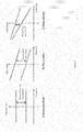
- Figure 1 illustrates the operation principle of analog adjustable attenuator/gain, phase, and delay.
- the graphs illustrate what happens to the signal at the output of individual signal processing element over broadband.
- the adjustable attenuator/gain is broadband device but it does not alter the delay or phase offset while attenuation/gain is changed.
- the adjustable phase shifter is also ideally a broadband device but it only adjusts the signal phase offset. Hence, delay and attenuation are not changed while the phase offset is changed.
- the delay adjustment circuit can adjust the delay, namely adjust the phase response slope, but the attenuation and phase offset remains unchanged. All these signal processing tasks can be performed today with several different analog circuit methods. There are significant number of different adjustable attenuator/amplifier circuits, phase sifters and delay adjustment circuits.
- Reflection type I&Q vector modulator for example, can adjust phase offset and attenuation independently.
- complex gain element can be achieved.
- Adjustable attenuator/gain cannot adjust amplitude slope or ripple over a target band.
- a phase shifter cannot adjust phase slope or ripple over a target band and a delay element cannot adjust phase offset over a target band, only phase slope is adjusted.
- US 6252461 discloses a method and a circuit for power amplification over a wide frequency range based upon the use of minimum-rating filters or matching networks, negative-component signal processing, and single or multiple amplifiers.
- the filters and matching networks are preferably designed to minimize the required ratings of the amplifier(s) driving them.
- the signal processor or generator preferably uses negative components to produces a driving signal that is compensated for the ripple in the filter, matching network, and load.
- the outputs of multiple amplifiers optimized for different frequency ranges can be combined into a single load with flat frequency response, resistive loads presented to the amplifiers, and no inherent power loss in the combining network.
- US 2015/155899 discloses a wideband radio frequency interference cancellation system that includes an electronic channel canceller configured to split an electronic reference signal output from an electronic transmitting element into a plurality of band signals. At least one electronic band pass filter is configured to receive a respective band signal delivered to a respective channel. The wideband RF interference cancellation system further includes at least one electronic tunable cancellation element configured to tune the respective channel such that reflections are canceled before being input to receiving element.
- a method can include splitting an input signal into a plurality of signal paths.
- the method can also include complex weighting, for each signal path, a respective signal.
- the method can further include summing outputs of the signal paths.
- the method can additionally include providing an output comprising the sum of the signal paths.
- the complex weighting can be configured to independently control gain, phase and delay of the output signal over broadband.
- an apparatus can include a splitter configured to split an input signal into a plurality of signal paths at a first end of the signal paths. Each signal path can include at least one attenuator and at least one delay element. The apparatus can also include a summer configured to sum the signal paths at a second end of the signal paths opposite the first end of the signal paths. The apparatus can be configured to independently control gain, phase and delay of the output signal over broadband.
- An apparatus can include means for splitting an input signal into a plurality of signal paths.
- the apparatus can also include means for complex weighting, for each signal path, a respective signal.
- the apparatus can further include means for summing outputs of the signal paths.
- the apparatus can additionally include means for providing an output comprising the sum of the signal paths.
- the complex weighting can be configured to independently control gain, phase and delay of the output signal over broadband.
- An apparatus can include means for splitting an input signal into a plurality of signal paths.
- the apparatus can also include means for complex weighting, for each signal path, a respective signal.
- the apparatus can include means for summing outputs of the signal paths.
- the apparatus can additionally include means for providing an output comprising the sum of the signal paths.
- Each of the complex weighted signal paths may have an individual filter.
- Certain embodiments relate to telecommunication system frequency response and delay control at analog domain. More particularly, certain embodiments relate to analog domain signal processing (ASP) circuit within telecommunication system. Circuit architecture capable of adjusting amplitude response, phase response and group delay over broadband is presented. The circuit could be called continuous-time filter or analog FIR filter depending on how the circuit elements are selected and dimensioned.
- ASP analog domain signal processing
- Certain embodiments provide circuitry that is capable of controlling gain, phase and delay over broadband with flexibility and independency of each other.
- Certain embodiments of an ASP-circuit can be used to combine all the above signal processing tasks and each task can be performed independently over broad bandwidth. Also, simplified versions of certain embodiments can perform simpler tasks but over broadband.
- Certain embodiments of the described ASP-circuits can be considered to belong to a group of analog domain finite impulse response (FIR)-like filters or into group of continuous-time filters.
- FIR finite impulse response
- Certain embodiments can adjust the circuit nominal delay within the limits set by the fractional delays and used coefficient type and number of signal paths. This process can be referred to as sinc-interpolation. There may be significant difference in the circuit frequency response tuning capabilities depending on what kind of fractional delays and weighting coefficients are used, and how many FIR-taps are used.
- an ASP-circuit can contain more than one nominal delay and a group of fractional delayed and complex weighted signal paths. Thus, it is possible to cancel signals with more than one dominant delay. For example, in TX leakage signal cancellation there may be two different delayed reflection signals within an RX path.
- certain embodiments of the ASP-circuit may provide a way to independently adjust signal amplitude, phase and delay response over broadband.
- Certain embodiments split the wanted input signal, for example a copy of a TX signal, into N couple of individual signal paths.
- Each individual signal path can then have adjustable analog circuit elements with the characteristics of attenuators/amplifiers, amplitude and phase shifters/vector modulators.
- each of the individual signal paths can have an analog delay element whose delay may be an integer multiple of a pre-defined fixed delay or may be selected individually for each independent signal path.
- each of the independent signal paths may contain an individual analog filter.
- the outputs of each independent signal path with selected tenable analog elements can be summed/subtracted to form the final output of the ASP-circuit.
- a desired ASP function can be achieved by defining the number of signal paths and elements within each path.
- the tuning range of the ASP-circuit can also be defined with those selections.
- certain embodiments of the ASP-circuit can be adaptive and can be optimized for a target system, based on a desired input-output function and tuning range.
- the adaptation of the ASP-circuit can also reduce the non-ideal effects within the ASP-circuit itself.
- Figure 2 shows a general architecture of an ASP-circuit according to certain embodiments.
- the filters within each isolated signal path can be considered to be part of natural per signal path characteristics or the filters can be implemented intentionally.
- the ASP-circuit can be split to perform ASP task for both carriers independently.
- the filters could be used to isolate the carriers from each other in such a case.
- the fractional delay elements can be used to construct more than one nominal delay.
- the fractional delays can be delay differences related to the nominal delay. This way, the input signal can be split into more than one fractional tunable signal paths. For example, a group of N-M signal paths can be used to adjust frequency response of one delay and a group of M signal paths can be used to adjust frequency response of other delay, and so on.
- Certain embodiments may be able to adjust at continuous-time domain the output signal amplitude response, phase response and delay response over broad band.
- ⁇ is the angular frequency of interest
- h N defines per signal path weight
- ⁇ N defines per signal path delay
- and arg( H N ( ⁇ , h N )) represent the amplitude and phase response of individual signal path.
- the output delay can still be adjusted by adjusting the coefficient values h N .
- the coefficients h N can be expressed within the frequency response function due to the nature of analog solution and due to the presence of possible per signal path additive filter.
- the DSP FIR responses as a function of per delay path weighting h N can be determined according to any way described in typical textbooks. Similarly, coefficients can be selected based on desired fractional delay, low pass filter and so on. Within DSP there is also ideal isolation between differently delayed signal paths. In certain cases, reasonable isolation may be achieved within the analog solution as well. Due to the analog solution, in reality each signal path may be slightly affected by all signal weights, delay selection and input signal amplitude because in practice there may not be perfect isolation nor perfect linearity nor RF match. Simplifications and linear analysis can be used to for purposes of explanation and illustration without requiring perfection in practice.
- Non-idealities can be such that the non-idealities can be minimized through implementation design. Moreover, non-idealities may be partly minimized within the adaptation process as well, when the ASP-circuit is used within a system.
- the implementation can also define nominal electrical delay that is not shown within the expression. Such delay can be considered to be part of each fractional delay element. Therefore, the delay can be adjusted around the total nominal delay. In case of complex coefficients, negative group delay can also be achieved.
- Certain embodiments may be able to adjust the output delay independently, to provide a desired group delay.
- the target delay r t can be approximated by summing suitable weighted and delayed signals.
- the sinc-function which is time sifted so that the peak value occurs at the location of the target delay ⁇ t .
- the solution in (1) can be used to produce fractional delay.
- the FIR filter impulse response, and the corresponding weighting values hN can be samples of continuous-time sinc-function whose peak value is shifted in time to the target delay location. That delay can be generated with the selected FIR coefficients.
- the number of required FIR coefficients would be infinite.
- the number of FIR taps can be reduced and the value of each remaining coefficient can be slightly altered so that the target delay is achieved while maintaining maximally flat amplitude response.
- the same fractional delay functionality can be achieved in certain ASP-circuits according to certain embodiments, when the per signal path unit delays are integer multiples of a pre-defined unit delay.
- This pre-defined unit delay can be designated as Ts in this example.
- Some of the n ⁇ Ts delayed signal paths would be shorter than the nominal delay and some would be longer than the nominal delay, some signal paths may have delay equal to the nominal delay.
- the circuit nominal delay can be altered.
- Figure 3 shows an ideal delay element impulse response curve for example target delays of 1 ⁇ Ts and 1.3 ⁇ Ts.
- Corresponding target delay can be approximated and produced with FIR having coefficient values hn (h0, h1, ...hn ⁇ Ts) defined as samples of the ideal delay impulse response curve at corresponding n ⁇ Ts time interval).
- Figure 3 illustrates FIR coefficients as samples of system impulse response, with delay examples, where Ts corresponds to AFIR unit delay.
- Figure 3 shows, as dots, nine first ideal required per signal path weighting values of target delay output of 1 ⁇ Ts and 1.3 ⁇ Ts. These values can be called FIR coefficients while the system is a continuous-time solution. As can be seen, when the unit delay Ts is fixed, one can adjust the system output nominal delay.
- the so called sinc-interpolation based fractional delay adjustment described above can provide the possibility to get wanted fractional delay output but at the same time can force the amplitude response to be ideally unity, while the phase response can be defined by the target delay. This may be not satisfactory because, for example in the case of full-duplex radio, the phase offset and amplitude response may need to be adjusted as well, over broadband.
- Two systems with equal delay do not necessarily have the same phase offset.
- a basic amplifier may have the same delay as a portion of transmission line at a target frequency or band but the phase may be up to 180 degree different due to an active device, bias and matching related phase shifts.
- certain embodiments provide for complex coefficients. Also, within certain embodiments all signal paths may have the strongest signal. This may be useful for wide delay adjustment range because the strongest or two strongest signals may be nearest to the target nominal delay, as seen in Figure 3 .
- the target delay would be exactly 4 ⁇ Ts, then only the 4th signal path may be used, while all others may be zeroed.
- Such wide delay adjustment range may not be possible if each signal path cannot contain the strongest signal.
- certain embodiments can adjust all three target parameters independently, amplitude response, phase response and delay within limitations of selected ASP-circuit element values and number of signal paths. Even negative group delay can be achieved.
- the system can achieve constant group delay phase shifter response or constant group delay amplitude slope adjuster response while using real valued weighting coefficients.
- benefit may arise from the 90 degree electrical unit delay and by selecting the coefficients as shown in Figure 4 . With these coefficient values, broadband vector modulator output may be achieved while using real valued coefficients, including bi-phase attenuators/gain elements.
- Figure 4 illustrates coefficients values of three-coefficient AFIR VM for 0-360 degree output phase rotation, according to certain embodiments.
- the output phase can be rotated while keeping the output magnitude relatively constant if one uses coefficients values shown in Figure 4 .
- the first signal path (h0) has zero delay
- the second signal path (h1) has 90 degree delay
- the 3 rd signal path (h3) has 180 degree delay.
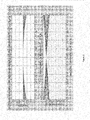
- Figure 5 illustrates corresponding amplitude and group delay response for 0 - 360 degree phase shift, according to certain embodiments.
- Ts 1/(2.5GHz).
- FIG. 6 illustrates three-coefficient AFIR based gain slope adjustment with constant group delay, according to certain embodiments.
- the AFIR structure can be the same as above.
- a difference can be that now the corner coefficients (h0 and h2) may have the same polarity but equal amplitude.
- Figure 6 shows example simulation results.
- one can add more odd stages for a still more broadband solution than illustrated.
- the output can be scaled just by scaling each coefficient with same scaling factor.
- Certain embodiments can be implemented in various ways. The implementations may depend on a desired complexity of frequency response adjustments.
- One complex case may be systems with broadband signals. Within these cases, there can be more than one dominant delay.
- the ASP-circuit according to certain embodiments can be used to generate more than one adjustable dominant delay, for example two nominal delays can be dimensioned and the unit delays can be integrated within those nominal delays.
- group of N-M signal paths can be adapted with one nominal delay and fractional delays, while the other group of M signal paths with other nominal delay and fractional delays can be adapted to different nominal delay (refer to Figure 2 and equation (1) keeping in mind that group of M fractional delays have different nominal delay).
- Sinc-interpolation may involve more than one fractional delay, if the target delay is not exactly an integer number of one unit delay. Hence, sinc-interpolation may be performed for two different delayed signal paths.
- Certain embodiments may involve various aspects. For example, certain embodiments may involve splitting the input signal into N couple of signal paths, complex weighting each signal path signal, fractional delaying each signal within individual signal path, possibly filtering each signal path signal and summing the signal path's outputs.
- Ts can be the unit delay.
- Such long unit delay is uncommon to DSP FIR solutions because usually high oversampling is required, so that flat amplitude response filters can be achieved.
- Figure 7 illustrates an example three-coefficient AFIR architecture, according to certain embodiments.
- This architecture may produce the output according to equation (1), set forth above.
- the AFIR coefficients can be real valued with plus and minus polarity.
- the unit delay can be 90 degree and three isolated signal paths can be used.
- the nominal delay can be that of the middle signal path from the input to the output.
- a system employing this architecture may be able to perform 0-360 degree phase adjustment while keeping constant group delay and flat frequency response.
- the coefficient values can be those shown in Figure 4 above, or directly relative to those through scaling. The coefficient values are described relative to each other.
- the same architecture can be used to perform constant group delay amplitude slope adjuster response, similar to the one shown in Figure 6 above.
- the input and output Wilkinson devices could be replaced with three-way Wilkinson devices, or other devices can also be used.
- Figure 8 illustrates a three-complex-coefficients AFIR while using real valued coefficients architecture according to certain embodiments.
- the 3-TAP real-valued element (RE) AFIR(hni,hnq) refers to the 3-coefficient AFIR circuit shown in Figure 7 .
- the hni and hnq refers to in phase and out of phase (90 degree) signal path coefficients.
- Both of the 3-TAP RE AFIR blocks can have equal group delay but the input signal can be in 90 degree phase offset. Therefore, the architecture of Figure 8 can be used to adjust both amplitude slope and phase offset (0-360) independently.
- the upper branch can produce the phase offset as shown in Figure 4 and 5
- the lower signal path can be used to produce amplitude slope.
- the outputs of individual AFIRs have the same group delay and because of isolation the total sum output signal is such that both output phase and amplitude slope can be adjusted independently.
- vector modulator and amplitude slope adjustment capability is achieved without using vector modulator.
- Vector modulator generally cannot be used to adjust amplitude slope.
- the solution can be broad band. These examples are based on a 90 degree unit delay selection. If the unit delay is not 90 degrees, then the solution can be varied accordingly.
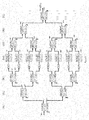
- Figure 9 illustrates an example AFIR architecture block diagram or ASP-circuit, according to certain embodiments.
- the 90 degree unit delay can still be used. However, due to the delay selection, the system can again effectively achieve complex gain weighting while using only bi-phase attenuators/gain elements. Each signal path group of two having equal fractional delay can form effectively complex gain, or AFIR weight, while using real valued coefficients.
- FIG. 10 illustrates another example AFIR architecture block diagram or ASP-circuit, according to certain embodiments.
- VM can be I&Q vector modulators, or VM can be 3-coefficient circuit, for example as shown in Figure 8 .
- the unit delay is illustrated as 90 degrees, although this embodiment may not be dependent on such unit delay being used.
- Each input signal path to the inputs of unit delay elements can have equal power attenuation.
- certain embodiments may have above one unit delay element delay adjustment range while being able to adjust amplitude and phase response as well.
- Certain embodiments can be tuned within an adaptation loop.
- the adaptation can depend on the target use of the ASP-circuit of certain embodiments.
- the adaptation may not purely rely on a time domain signal. Instead, the frequency content of the signals within the adaptation may be useful for performance optimization in a wanted band.
- Certain embodiments may provide a generic ASP-circuit capable of performing FIR-like responses. Therefore, certain embodiments may be integrated as part of many telecommunication systems. For example, certain embodiments may be applied to any system that contains analog domain feedforwarding or system where amplitude and/or phase and/or delay response is adjusted at analog domain. For example within analog domain controlled beamforming solutions, certain embodiments may be deployed.
- Figure 11 illustrates a method according to certain embodiments.
- the method of Figure 11 can be configured to operate at continuous-time domain.
- a method can include, at 1110, splitting an input signal into a plurality of signal paths. These may be the various plurality of paths illustrated in Figures 2 and 7-10 .
- the method can also include, at 1120, complex weighting, for each signal path, a respective signal. This complex weighting can further be combined with fractionally delaying, at 1125, each respective signal for each signal path. The elements used for such complex weighting and fractional delaying can be seen illustrated, for example, in Figures 2 and 7-10 .
- the complex weighting can further be combined with, at 1127, filtering the respective signal for each signal path.
- the method can further include, at 1130, summing outputs of the signal paths.
- the method can additionally include, at 1140, providing an output comprising the sum of the signal paths.
- the output can be provided to any feedforward system, such as a transceiver, antenna, or any other communication circuit.
- the complex weighting together with the delaying and filtering, can be configured to independently control gain, phase and delay of the output signal over broadband.
- certain embodiments may provide a tunable system.
- the fractionally delaying described above can include delaying by one quarter wavelength.
- the fractional delay in different signal paths can differ from one another.
- the method can also include, at 1150, tuning at least one of the gain, phase and delay independently by adjusting at least one of the complex weighting or the fractional delaying.
- the filtering can also be tuned, if desired, and such filtering can also be used in the tuning of gain, phase, and delay.
- FIG 12 illustrates a system according to certain embodiments of the invention. It should be understood that each block of the diagrams of Figures 2 and 7-11 may be implemented by various means or their combinations, such as hardware, software, firmware, one or more processors and/or circuitry. As noted above, analog circuitry may be one way by which many of the described features are implemented, although other elements may be added, or certain analog elements may be replaced by digital elements.
- a system may include several devices, such as, for example, network element 1210 and user equipment (UE) or user device 1220.
- the system may include more than one UE 1220 and more than one network element 1210, although only one of each is shown for the purposes of illustration.
- a network element can be an access point, a base station, an eNode B (eNB), or any other network element.
- Each of these devices may include at least one processor or control unit or module, respectively indicated as 1214 and 1224.
- At least one memory may be provided in each device, and indicated as 1215 and 1225, respectively.
- the memory may include computer program instructions or computer code contained therein, for example for carrying out the embodiments described above.
- Each device may also include an antenna, respectively illustrated as 1217 and 1227. Although only one antenna each is shown, many antennas and multiple antenna elements may be provided to each of the devices. Other configurations of these devices, for example, may be provided.
- network element 1210 and UE 1220 may be additionally configured for wired communication, in addition to wireless communication, and in such a case antennas 1217 and 1227 may illustrate any form of communication hardware, without being limited to merely an antenna.
- Transceivers 1216 and 1226 may each, independently, be a transmitter, a receiver, or both a transmitter and a receiver, or a unit or device that may be configured both for transmission and reception.
- the transmitter and/or receiver (as far as radio parts are concerned) may also be implemented as a remote radio head which is not located in the device itself, but in a mast, for example.
- the operations and functionalities may be performed in different entities, such as nodes, hosts or servers, in a flexible manner. In other words, division of labor may vary case by case.
- One possible use is to make a network element to deliver local content.
- One or more functionalities may also be implemented as a virtual application that is provided as software that can run on a server.
- a user device or user equipment 1220 may be a mobile station (MS) such as a mobile phone or smart phone or multimedia device, a computer, such as a tablet, provided with wireless communication capabilities, personal data or digital assistant (PDA) provided with wireless communication capabilities, portable media player, digital camera, pocket video camera, navigation unit provided with wireless communication capabilities or any combinations thereof.
- MS mobile station
- PDA personal data or digital assistant
- the user device or user equipment 1220 may be a sensor or smart meter, or other device that may usually be configured for a single location.
- an apparatus such as a node or user device, may include means for carrying out embodiments described above in relation to Figures 2 and 7-11 .
- Processors 1214 and 1224 may be embodied by any computational or data processing device, such as a central processing unit (CPU), digital signal processor (DSP), application specific integrated circuit (ASIC), programmable logic devices (PLDs), field programmable gate arrays (FPGAs), digitally enhanced circuits, or comparable device or a combination thereof.
- the processors may be implemented as a single controller, or a plurality of controllers or processors. Additionally, the processors may be implemented as a pool of processors in a local configuration, in a cloud configuration, or in a combination thereof.
- the implementation may include modules or unit of at least one chip set (e.g., procedures, functions, and so on).
- Memories 1215 and 1225 may independently be any suitable storage device, such as a non-transitory computer-readable medium.
- a hard disk drive (HDD), random access memory (RAM), flash memory, or other suitable memory may be used.
- the memories may be combined on a single integrated circuit as the processor, or may be separate therefrom.
- the computer program instructions may be stored in the memory and which may be processed by the processors can be any suitable form of computer program code, for example, a compiled or interpreted computer program written in any suitable programming language.
- the memory or data storage entity is typically internal but may also be external or a combination thereof, such as in the case when additional memory capacity is obtained from a service provider.
- the memory may be fixed or removable.
- a non-transitory computer-readable medium may be encoded with computer instructions or one or more computer program (such as added or updated software routine, applet or macro) that, when executed in hardware, may perform a process such as one of the processes described herein.
- Computer programs may be coded by a programming language, which may be a high-level programming language, such as objective-C, C, C++, C#, Java, etc., or a low-level programming language, such as a machine language, or assembler. Alternatively, certain embodiments of the invention may be performed entirely in hardware.
- Figure 12 illustrates a system including a network element 1210 and a UE 1220
- embodiments of the invention may be applicable to other configurations, and configurations involving additional elements, as illustrated and discussed herein.
- multiple user equipment devices and multiple network elements may be present, or other nodes providing similar functionality, such as nodes that combine the functionality of a user equipment and an access point, such as a relay node.
Landscapes
- Engineering & Computer Science (AREA)
- Signal Processing (AREA)
- Computer Networks & Wireless Communication (AREA)
- Power Engineering (AREA)
- Physics & Mathematics (AREA)
- General Physics & Mathematics (AREA)
- Networks Using Active Elements (AREA)
- Amplifiers (AREA)
Claims (11)
- Verfahren zur Übertragungslecksignalauslöschung in der analogen Domäne, wobei das Verfahren Folgendes umfasst:Teilen (1110) eines Eingangssignals in mehrere Signalpfade, wobei das Eingangssignal eine Kopie eines Übertragungssignals ist;komplexes Gewichten (1120) und Verzögern eines jeweiligen Signals für jeden Signalpfad;Summieren (1130) von Ausgängen der Signalpfade, und Bereitstellen (1140) eines Ausgangs, der die Summe der Signalpfade umfasst, wobei das Ausgangssignal zu Empfängerpfaden vorwärts eingekoppelt wird, um Übertragungssignalleckverlust auszulöschen,dadurch gekennzeichnet, dass das komplexe Gewichten und Verzögern ausgebildet sind zum unabhängigen Steuern von Verstärkung, Phase und Verzögerung des Ausgangssignals über Breitband,und dass das Verfahren ferner Folgendes umfasst:
fraktionales Verzögern (1125) jedes jeweiligen Signals für jeden Signalpfad, wobei eine Verzögerung jedes der mehreren Signalpfade einzeln für jeden der mehreren Signalpfade ausgewählt wird. - Verfahren nach Anspruch 1, wobei das fraktionale Verzögern Verzögern um eine Viertelwellenlänge umfasst.
- Verfahren nach Anspruch 1, das ferner Folgendes umfasst:
unabhängiges Abstimmen (1150) der Verzögerung durch Anpassen der fraktionalen Verzögerung. - Verfahren nach Anspruch 1, das ferner Folgendes umfasst:
Filtern (1127) des jeweiligen Signals für jeden Signalpfad. - Verfahren nach Anspruch 1, wobei das Verfahren ausgebildet ist zum Arbeiten an der zeitkontinuierlichen Domäne.
- Vorrichtung zur Übertragungslecksignalauslöschung in der analogen Domäne, wobei die Vorrichtung Folgendes umfasst:einen Teiler, der ausgebildet ist zum Teilen (1110) eines Eingangssignals in mehrere Signalpfade an einem ersten Ende der Signalpfade, wobei jeder Signalpfad mindestens ein Dämpfungsglied und mindestens ein Verzögerungselement umfasst, wobei das Eingangssignal eine Kopie eines Übertragungssignals ist; undeinen Summierer, der ausgebildet ist zum Summieren (1130) der Signalpfade an einem zweiten Ende der Signalpfade entgegengesetzt zu dem ersten Ende der Signalpfade, wobei ein Ausgangssignal zu Empfängerpfaden vorwärts eingekoppelt wird, um Übertragungssignalleckverlust auszulöschen,dadurch gekennzeichnet, dassdie Vorrichtung ausgebildet ist zum unabhängigen Steuern von Verstärkung, Phase und Verzögerung des Ausgangssignals über Breitband mittels komplexem Gewichten und Verzögern,und dass das Verzögerungselement für jeden Signalpfad ausgebildet ist zum fraktionalen Verzögern (1125) eines jeweiligen Signals für jeden Signalpfad, wobei eine Verzögerung jedes der mehreren Signalpfade einzeln für jeden der mehreren Signalpfade ausgewählt wird.
- Vorrichtung nach Anspruch 6, wobei das fraktionale Verzögern Verzögern um eine Viertelwellenlänge umfasst.
- Vorrichtung nach Anspruch 6, wobei die Vorrichtung ausgebildet ist zum unabhängigen Abstimmen der Verzögerung durch Anpassen der fraktionalen Verzögerung.
- Vorrichtung nach Anspruch 6, die ferner ein Filter für jeden Signalpfad umfasst, das ausgebildet ist zum Filtern (1127) des jeweiligen Signals für jeden Signalpfad.
- Vorrichtung nach Anspruch 6, wobei die Vorrichtung ausgebildet ist zum Arbeiten an der zeitkontinuierlichen Domäne.
- Vorrichtung nach Anspruch 6, wobei die mehreren Signalpfade mindestens drei Signalpfade umfassen.
Applications Claiming Priority (1)
| Application Number | Priority Date | Filing Date | Title |
|---|---|---|---|
| US14/829,310 US10027367B2 (en) | 2015-08-18 | 2015-08-18 | Quarter wavelength unit delay and complex weighting coefficient continuous-time filters |
Publications (2)
| Publication Number | Publication Date |
|---|---|
| EP3133787A1 EP3133787A1 (de) | 2017-02-22 |
| EP3133787B1 true EP3133787B1 (de) | 2020-07-22 |
Family
ID=56263529
Family Applications (1)
| Application Number | Title | Priority Date | Filing Date |
|---|---|---|---|
| EP16175610.1A Active EP3133787B1 (de) | 2015-08-18 | 2016-06-22 | Zeitkontinuierliche filter mit viertelwelleneinheitsverzögerung und komplex gewichteten koeffizienten |
Country Status (3)
| Country | Link |
|---|---|
| US (1) | US10027367B2 (de) |
| EP (1) | EP3133787B1 (de) |
| CN (1) | CN106470098A (de) |
Families Citing this family (6)
| Publication number | Priority date | Publication date | Assignee | Title |
|---|---|---|---|---|
| US10904042B2 (en) | 2017-09-29 | 2021-01-26 | Tektronix, Inc. | Passive variable continuous time linear equalizer with attenuation and frequency control |
| JP7558642B2 (ja) * | 2018-02-05 | 2024-10-01 | テクトロニクス・インコーポレイテッド | ノイズ・フィルタ及びノイズ低減方法 |
| KR102810894B1 (ko) * | 2019-06-27 | 2025-05-20 | 시놉시스, 인크. | 데이터 포인트들의 보간을 사용한 파형 구성 |
| CN110798175B (zh) * | 2019-11-08 | 2023-03-10 | 大连海事大学 | 一种基于负群时延电路的宽带线性相位滤波器 |
| CN119678375A (zh) * | 2022-08-18 | 2025-03-21 | 德州仪器公司 | 用于反射均衡的可变延迟fir滤波器 |
| US12580599B2 (en) * | 2022-08-18 | 2026-03-17 | Texas Instruments Incorporated | Variable delay FIR filter for reflection equalization |
Family Cites Families (18)
| Publication number | Priority date | Publication date | Assignee | Title |
|---|---|---|---|---|
| US5844139A (en) * | 1996-12-30 | 1998-12-01 | General Electric Company | Method and apparatus for providing dynamically variable time delays for ultrasound beamformer |
| US6047022A (en) | 1997-02-28 | 2000-04-04 | Orckit Communication Ltd. | Apparatus and method for transmission of high speed data over communication channels |
| US6252461B1 (en) | 1997-08-25 | 2001-06-26 | Frederick Herbert Raab | Technique for wideband operation of power amplifiers |
| US6658045B1 (en) | 1999-02-22 | 2003-12-02 | Nortel Networks Limited | CDMA communications system adaptive to mobile unit speed |
| US6587514B1 (en) | 1999-07-13 | 2003-07-01 | Pmc-Sierra, Inc. | Digital predistortion methods for wideband amplifiers |
| US6392481B1 (en) | 1999-11-30 | 2002-05-21 | Nokia Networks Oy | Method and apparatus for improved fed forward amplification |
| US6580771B2 (en) * | 2001-03-30 | 2003-06-17 | Nokia Corporation | Successive user data multipath interference cancellation |
| AU2002950621A0 (en) * | 2002-08-07 | 2002-09-12 | J I Peston Pty Ltd | Near-field antenna array with signal processing |
| US7583754B2 (en) | 2002-10-31 | 2009-09-01 | Zte Corporation | Method and system for broadband predistortion linearization |
| US7120561B2 (en) | 2002-12-18 | 2006-10-10 | Nokia Corporation | Phase-error based signal alignment |
| US7545859B2 (en) | 2004-01-14 | 2009-06-09 | L-3 Communications Integrated Systems L.P. | Adaptive channel equalization technique and method for wideband passive digital receivers |
| US7522011B2 (en) | 2005-08-15 | 2009-04-21 | Nokia Corporation | High pass modulation of a phase locked loop |
| US8208527B2 (en) | 2007-01-30 | 2012-06-26 | California Institute Of Technology | Scalable reconfigurable concurrent filter for wide-bandwidth communication |
| US7995697B2 (en) | 2007-06-18 | 2011-08-09 | Infineon Technologies Ag | Polar modulation / one-point frequency modulation with flexible reference frequency |
| US8154445B2 (en) * | 2010-03-30 | 2012-04-10 | Raytheon Company | System and method for frequency domain correction of global navigation satellite system pseudorance measurements in receivers having controlled reception pattern antennas |
| EP2538167A1 (de) | 2011-06-23 | 2012-12-26 | Nederlandse Organisatie voor toegepast -natuurwetenschappelijk onderzoek TNO | Explosions- und bruchsichere Wandabschnitte zur Verwendung in Strukturen wie Schiffen |
| WO2014121290A1 (en) | 2013-02-04 | 2014-08-07 | Kumu Networks | Signal cancellation using feedforward and feedback paths |
| US9479214B2 (en) | 2013-11-25 | 2016-10-25 | Raytheon Company | Wideband active radio frequency interference cancellation system |
-
2015
- 2015-08-18 US US14/829,310 patent/US10027367B2/en active Active
-
2016
- 2016-06-22 EP EP16175610.1A patent/EP3133787B1/de active Active
- 2016-08-18 CN CN201610682663.5A patent/CN106470098A/zh active Pending
Non-Patent Citations (1)
| Title |
|---|
| None * |
Also Published As
| Publication number | Publication date |
|---|---|
| EP3133787A1 (de) | 2017-02-22 |
| US10027367B2 (en) | 2018-07-17 |
| US20170054469A1 (en) | 2017-02-23 |
| CN106470098A (zh) | 2017-03-01 |
Similar Documents
| Publication | Publication Date | Title |
|---|---|---|
| EP3133787B1 (de) | Zeitkontinuierliche filter mit viertelwelleneinheitsverzögerung und komplex gewichteten koeffizienten | |
| US8990279B2 (en) | Filter shaping using a signal cancellation function | |
| US11128329B2 (en) | Systems and methods for configurable hybrid self-interference cancellation | |
| US9490963B2 (en) | Signal cancellation using feedforward and feedback paths | |
| US8805298B2 (en) | Transceiver with compensation for transmit signal leakage and method therefor | |
| US9455756B2 (en) | Systems and methods for frequency independent analog self-interference cancellation | |
| KR102106232B1 (ko) | 동시 송신 및 수신을 위한 이산 시간 아날로그 신호 처리 | |
| US9866267B2 (en) | Devices and methods for diversity signal enhancement and cosite cancellation | |
| CN103190076A (zh) | 可调谐滤波器设备和方法 | |
| US9906262B2 (en) | All-analog and hybrid radio interference cancellation using cables, attenuators and power splitters | |
| US10644813B2 (en) | Antenna array calibration method and apparatus | |
| EP3257164B1 (de) | Signalisolierungsteuerungsvorrichtung und verfahren zur steuerung einer hybriden verbindung | |
| EP3055946B1 (de) | Signalverarbeitungsvorrichtung, verstärker und verfahren | |
| US9065425B2 (en) | Feed-forward linearization without phase shifters | |
| KR102076745B1 (ko) | 벡터 모듈레이터를 이용한 간섭 제거 장치, 시스템 및 방법 | |
| Ahmed et al. | Baseband equalizer for TX leakage cancellation in active duplexing |
Legal Events
| Date | Code | Title | Description |
|---|---|---|---|
| PUAI | Public reference made under article 153(3) epc to a published international application that has entered the european phase |
Free format text: ORIGINAL CODE: 0009012 |
|
| STAA | Information on the status of an ep patent application or granted ep patent |
Free format text: STATUS: THE APPLICATION HAS BEEN PUBLISHED |
|
| AK | Designated contracting states |
Kind code of ref document: A1 Designated state(s): AL AT BE BG CH CY CZ DE DK EE ES FI FR GB GR HR HU IE IS IT LI LT LU LV MC MK MT NL NO PL PT RO RS SE SI SK SM TR |
|
| AX | Request for extension of the european patent |
Extension state: BA ME |
|
| STAA | Information on the status of an ep patent application or granted ep patent |
Free format text: STATUS: REQUEST FOR EXAMINATION WAS MADE |
|
| 17P | Request for examination filed |
Effective date: 20170822 |
|
| RBV | Designated contracting states (corrected) |
Designated state(s): AL AT BE BG CH CY CZ DE DK EE ES FI FR GB GR HR HU IE IS IT LI LT LU LV MC MK MT NL NO PL PT RO RS SE SI SK SM TR |
|
| STAA | Information on the status of an ep patent application or granted ep patent |
Free format text: STATUS: EXAMINATION IS IN PROGRESS |
|
| 17Q | First examination report despatched |
Effective date: 20181115 |
|
| RAP1 | Party data changed (applicant data changed or rights of an application transferred) |
Owner name: NOKIA SOLUTIONS AND NETWORKS OY |
|
| GRAP | Despatch of communication of intention to grant a patent |
Free format text: ORIGINAL CODE: EPIDOSNIGR1 |
|
| STAA | Information on the status of an ep patent application or granted ep patent |
Free format text: STATUS: GRANT OF PATENT IS INTENDED |
|
| INTG | Intention to grant announced |
Effective date: 20200128 |
|
| GRAS | Grant fee paid |
Free format text: ORIGINAL CODE: EPIDOSNIGR3 |
|
| GRAA | (expected) grant |
Free format text: ORIGINAL CODE: 0009210 |
|
| STAA | Information on the status of an ep patent application or granted ep patent |
Free format text: STATUS: THE PATENT HAS BEEN GRANTED |
|
| AK | Designated contracting states |
Kind code of ref document: B1 Designated state(s): AL AT BE BG CH CY CZ DE DK EE ES FI FR GB GR HR HU IE IS IT LI LT LU LV MC MK MT NL NO PL PT RO RS SE SI SK SM TR |
|
| REG | Reference to a national code |
Ref country code: GB Ref legal event code: FG4D |
|
| REG | Reference to a national code |
Ref country code: CH Ref legal event code: EP |
|
| REG | Reference to a national code |
Ref country code: DE Ref legal event code: R096 Ref document number: 602016040283 Country of ref document: DE |
|
| REG | Reference to a national code |
Ref country code: AT Ref legal event code: REF Ref document number: 1294457 Country of ref document: AT Kind code of ref document: T Effective date: 20200815 |
|
| REG | Reference to a national code |
Ref country code: IE Ref legal event code: FG4D |
|
| REG | Reference to a national code |
Ref country code: NL Ref legal event code: FP |
|
| REG | Reference to a national code |
Ref country code: LT Ref legal event code: MG4D |
|
| REG | Reference to a national code |
Ref country code: AT Ref legal event code: MK05 Ref document number: 1294457 Country of ref document: AT Kind code of ref document: T Effective date: 20200722 |
|
| PG25 | Lapsed in a contracting state [announced via postgrant information from national office to epo] |
Ref country code: FI Free format text: LAPSE BECAUSE OF FAILURE TO SUBMIT A TRANSLATION OF THE DESCRIPTION OR TO PAY THE FEE WITHIN THE PRESCRIBED TIME-LIMIT Effective date: 20200722 Ref country code: SE Free format text: LAPSE BECAUSE OF FAILURE TO SUBMIT A TRANSLATION OF THE DESCRIPTION OR TO PAY THE FEE WITHIN THE PRESCRIBED TIME-LIMIT Effective date: 20200722 Ref country code: AT Free format text: LAPSE BECAUSE OF FAILURE TO SUBMIT A TRANSLATION OF THE DESCRIPTION OR TO PAY THE FEE WITHIN THE PRESCRIBED TIME-LIMIT Effective date: 20200722 Ref country code: HR Free format text: LAPSE BECAUSE OF FAILURE TO SUBMIT A TRANSLATION OF THE DESCRIPTION OR TO PAY THE FEE WITHIN THE PRESCRIBED TIME-LIMIT Effective date: 20200722 Ref country code: GR Free format text: LAPSE BECAUSE OF FAILURE TO SUBMIT A TRANSLATION OF THE DESCRIPTION OR TO PAY THE FEE WITHIN THE PRESCRIBED TIME-LIMIT Effective date: 20201023 Ref country code: NO Free format text: LAPSE BECAUSE OF FAILURE TO SUBMIT A TRANSLATION OF THE DESCRIPTION OR TO PAY THE FEE WITHIN THE PRESCRIBED TIME-LIMIT Effective date: 20201022 Ref country code: LT Free format text: LAPSE BECAUSE OF FAILURE TO SUBMIT A TRANSLATION OF THE DESCRIPTION OR TO PAY THE FEE WITHIN THE PRESCRIBED TIME-LIMIT Effective date: 20200722 Ref country code: ES Free format text: LAPSE BECAUSE OF FAILURE TO SUBMIT A TRANSLATION OF THE DESCRIPTION OR TO PAY THE FEE WITHIN THE PRESCRIBED TIME-LIMIT Effective date: 20200722 Ref country code: PT Free format text: LAPSE BECAUSE OF FAILURE TO SUBMIT A TRANSLATION OF THE DESCRIPTION OR TO PAY THE FEE WITHIN THE PRESCRIBED TIME-LIMIT Effective date: 20201123 Ref country code: BG Free format text: LAPSE BECAUSE OF FAILURE TO SUBMIT A TRANSLATION OF THE DESCRIPTION OR TO PAY THE FEE WITHIN THE PRESCRIBED TIME-LIMIT Effective date: 20201022 |
|
| PG25 | Lapsed in a contracting state [announced via postgrant information from national office to epo] |
Ref country code: PL Free format text: LAPSE BECAUSE OF FAILURE TO SUBMIT A TRANSLATION OF THE DESCRIPTION OR TO PAY THE FEE WITHIN THE PRESCRIBED TIME-LIMIT Effective date: 20200722 Ref country code: LV Free format text: LAPSE BECAUSE OF FAILURE TO SUBMIT A TRANSLATION OF THE DESCRIPTION OR TO PAY THE FEE WITHIN THE PRESCRIBED TIME-LIMIT Effective date: 20200722 Ref country code: RS Free format text: LAPSE BECAUSE OF FAILURE TO SUBMIT A TRANSLATION OF THE DESCRIPTION OR TO PAY THE FEE WITHIN THE PRESCRIBED TIME-LIMIT Effective date: 20200722 Ref country code: IS Free format text: LAPSE BECAUSE OF FAILURE TO SUBMIT A TRANSLATION OF THE DESCRIPTION OR TO PAY THE FEE WITHIN THE PRESCRIBED TIME-LIMIT Effective date: 20201122 |
|
| REG | Reference to a national code |
Ref country code: DE Ref legal event code: R097 Ref document number: 602016040283 Country of ref document: DE |
|
| PG25 | Lapsed in a contracting state [announced via postgrant information from national office to epo] |
Ref country code: EE Free format text: LAPSE BECAUSE OF FAILURE TO SUBMIT A TRANSLATION OF THE DESCRIPTION OR TO PAY THE FEE WITHIN THE PRESCRIBED TIME-LIMIT Effective date: 20200722 Ref country code: IT Free format text: LAPSE BECAUSE OF FAILURE TO SUBMIT A TRANSLATION OF THE DESCRIPTION OR TO PAY THE FEE WITHIN THE PRESCRIBED TIME-LIMIT Effective date: 20200722 Ref country code: DK Free format text: LAPSE BECAUSE OF FAILURE TO SUBMIT A TRANSLATION OF THE DESCRIPTION OR TO PAY THE FEE WITHIN THE PRESCRIBED TIME-LIMIT Effective date: 20200722 Ref country code: CZ Free format text: LAPSE BECAUSE OF FAILURE TO SUBMIT A TRANSLATION OF THE DESCRIPTION OR TO PAY THE FEE WITHIN THE PRESCRIBED TIME-LIMIT Effective date: 20200722 Ref country code: RO Free format text: LAPSE BECAUSE OF FAILURE TO SUBMIT A TRANSLATION OF THE DESCRIPTION OR TO PAY THE FEE WITHIN THE PRESCRIBED TIME-LIMIT Effective date: 20200722 Ref country code: SM Free format text: LAPSE BECAUSE OF FAILURE TO SUBMIT A TRANSLATION OF THE DESCRIPTION OR TO PAY THE FEE WITHIN THE PRESCRIBED TIME-LIMIT Effective date: 20200722 |
|
| PLBE | No opposition filed within time limit |
Free format text: ORIGINAL CODE: 0009261 |
|
| STAA | Information on the status of an ep patent application or granted ep patent |
Free format text: STATUS: NO OPPOSITION FILED WITHIN TIME LIMIT |
|
| PG25 | Lapsed in a contracting state [announced via postgrant information from national office to epo] |
Ref country code: AL Free format text: LAPSE BECAUSE OF FAILURE TO SUBMIT A TRANSLATION OF THE DESCRIPTION OR TO PAY THE FEE WITHIN THE PRESCRIBED TIME-LIMIT Effective date: 20200722 |
|
| 26N | No opposition filed |
Effective date: 20210423 |
|
| PG25 | Lapsed in a contracting state [announced via postgrant information from national office to epo] |
Ref country code: SK Free format text: LAPSE BECAUSE OF FAILURE TO SUBMIT A TRANSLATION OF THE DESCRIPTION OR TO PAY THE FEE WITHIN THE PRESCRIBED TIME-LIMIT Effective date: 20200722 |
|
| PGFP | Annual fee paid to national office [announced via postgrant information from national office to epo] |
Ref country code: NL Payment date: 20210615 Year of fee payment: 6 Ref country code: FR Payment date: 20210513 Year of fee payment: 6 |
|
| PG25 | Lapsed in a contracting state [announced via postgrant information from national office to epo] |
Ref country code: SI Free format text: LAPSE BECAUSE OF FAILURE TO SUBMIT A TRANSLATION OF THE DESCRIPTION OR TO PAY THE FEE WITHIN THE PRESCRIBED TIME-LIMIT Effective date: 20200722 |
|
| PG25 | Lapsed in a contracting state [announced via postgrant information from national office to epo] |
Ref country code: MC Free format text: LAPSE BECAUSE OF FAILURE TO SUBMIT A TRANSLATION OF THE DESCRIPTION OR TO PAY THE FEE WITHIN THE PRESCRIBED TIME-LIMIT Effective date: 20200722 |
|
| REG | Reference to a national code |
Ref country code: CH Ref legal event code: PL |
|
| REG | Reference to a national code |
Ref country code: BE Ref legal event code: MM Effective date: 20210630 |
|
| PG25 | Lapsed in a contracting state [announced via postgrant information from national office to epo] |
Ref country code: LU Free format text: LAPSE BECAUSE OF NON-PAYMENT OF DUE FEES Effective date: 20210622 |
|
| PG25 | Lapsed in a contracting state [announced via postgrant information from national office to epo] |
Ref country code: LI Free format text: LAPSE BECAUSE OF NON-PAYMENT OF DUE FEES Effective date: 20210630 Ref country code: IE Free format text: LAPSE BECAUSE OF NON-PAYMENT OF DUE FEES Effective date: 20210622 Ref country code: CH Free format text: LAPSE BECAUSE OF NON-PAYMENT OF DUE FEES Effective date: 20210630 |
|
| PG25 | Lapsed in a contracting state [announced via postgrant information from national office to epo] |
Ref country code: BE Free format text: LAPSE BECAUSE OF NON-PAYMENT OF DUE FEES Effective date: 20210630 |
|
| REG | Reference to a national code |
Ref country code: NL Ref legal event code: MM Effective date: 20220701 |
|
| PG25 | Lapsed in a contracting state [announced via postgrant information from national office to epo] |
Ref country code: NL Free format text: LAPSE BECAUSE OF NON-PAYMENT OF DUE FEES Effective date: 20220701 |
|
| PG25 | Lapsed in a contracting state [announced via postgrant information from national office to epo] |
Ref country code: FR Free format text: LAPSE BECAUSE OF NON-PAYMENT OF DUE FEES Effective date: 20220630 |
|
| PG25 | Lapsed in a contracting state [announced via postgrant information from national office to epo] |
Ref country code: HU Free format text: LAPSE BECAUSE OF FAILURE TO SUBMIT A TRANSLATION OF THE DESCRIPTION OR TO PAY THE FEE WITHIN THE PRESCRIBED TIME-LIMIT; INVALID AB INITIO Effective date: 20160622 |
|
| PG25 | Lapsed in a contracting state [announced via postgrant information from national office to epo] |
Ref country code: CY Free format text: LAPSE BECAUSE OF FAILURE TO SUBMIT A TRANSLATION OF THE DESCRIPTION OR TO PAY THE FEE WITHIN THE PRESCRIBED TIME-LIMIT Effective date: 20200722 |
|
| PG25 | Lapsed in a contracting state [announced via postgrant information from national office to epo] |
Ref country code: MK Free format text: LAPSE BECAUSE OF FAILURE TO SUBMIT A TRANSLATION OF THE DESCRIPTION OR TO PAY THE FEE WITHIN THE PRESCRIBED TIME-LIMIT Effective date: 20200722 |
|
| PG25 | Lapsed in a contracting state [announced via postgrant information from national office to epo] |
Ref country code: MT Free format text: LAPSE BECAUSE OF FAILURE TO SUBMIT A TRANSLATION OF THE DESCRIPTION OR TO PAY THE FEE WITHIN THE PRESCRIBED TIME-LIMIT Effective date: 20200722 |
|
| PGFP | Annual fee paid to national office [announced via postgrant information from national office to epo] |
Ref country code: DE Payment date: 20250429 Year of fee payment: 10 |
|
| PGFP | Annual fee paid to national office [announced via postgrant information from national office to epo] |
Ref country code: GB Payment date: 20250501 Year of fee payment: 10 |
|
| PG25 | Lapsed in a contracting state [announced via postgrant information from national office to epo] |
Ref country code: TR Free format text: LAPSE BECAUSE OF FAILURE TO SUBMIT A TRANSLATION OF THE DESCRIPTION OR TO PAY THE FEE WITHIN THE PRESCRIBED TIME-LIMIT Effective date: 20200722 |