EP3133617A1 - 3d shaped inductive charging coil and method of making the same - Google Patents
3d shaped inductive charging coil and method of making the same Download PDFInfo
- Publication number
- EP3133617A1 EP3133617A1 EP16178031.7A EP16178031A EP3133617A1 EP 3133617 A1 EP3133617 A1 EP 3133617A1 EP 16178031 A EP16178031 A EP 16178031A EP 3133617 A1 EP3133617 A1 EP 3133617A1
- Authority
- EP
- European Patent Office
- Prior art keywords
- coil
- layer
- insulating layer
- conductive
- coil assembly
- Prior art date
- Legal status (The legal status is an assumption and is not a legal conclusion. Google has not performed a legal analysis and makes no representation as to the accuracy of the status listed.)
- Granted
Links
Images




Classifications
-
- H—ELECTRICITY
- H01—ELECTRIC ELEMENTS
- H01F—MAGNETS; INDUCTANCES; TRANSFORMERS; SELECTION OF MATERIALS FOR THEIR MAGNETIC PROPERTIES
- H01F27/00—Details of transformers or inductances, in general
- H01F27/28—Coils; Windings; Conductive connections
- H01F27/32—Insulating of coils, windings, or parts thereof
- H01F27/327—Encapsulating or impregnating
-
- H—ELECTRICITY
- H01—ELECTRIC ELEMENTS
- H01F—MAGNETS; INDUCTANCES; TRANSFORMERS; SELECTION OF MATERIALS FOR THEIR MAGNETIC PROPERTIES
- H01F38/00—Adaptations of transformers or inductances for specific applications or functions
- H01F38/14—Inductive couplings
-
- H—ELECTRICITY
- H01—ELECTRIC ELEMENTS
- H01F—MAGNETS; INDUCTANCES; TRANSFORMERS; SELECTION OF MATERIALS FOR THEIR MAGNETIC PROPERTIES
- H01F27/00—Details of transformers or inductances, in general
- H01F27/28—Coils; Windings; Conductive connections
- H01F27/2804—Printed windings
-
- H—ELECTRICITY
- H01—ELECTRIC ELEMENTS
- H01F—MAGNETS; INDUCTANCES; TRANSFORMERS; SELECTION OF MATERIALS FOR THEIR MAGNETIC PROPERTIES
- H01F41/00—Apparatus or processes specially adapted for manufacturing or assembling magnets, inductances or transformers; Apparatus or processes specially adapted for manufacturing materials characterised by their magnetic properties
- H01F41/02—Apparatus or processes specially adapted for manufacturing or assembling magnets, inductances or transformers; Apparatus or processes specially adapted for manufacturing materials characterised by their magnetic properties for manufacturing cores, coils, or magnets
- H01F41/04—Apparatus or processes specially adapted for manufacturing or assembling magnets, inductances or transformers; Apparatus or processes specially adapted for manufacturing materials characterised by their magnetic properties for manufacturing cores, coils, or magnets for manufacturing coils
- H01F41/041—Printed circuit coils
- H01F41/046—Printed circuit coils structurally combined with ferromagnetic material
-
- H—ELECTRICITY
- H01—ELECTRIC ELEMENTS
- H01F—MAGNETS; INDUCTANCES; TRANSFORMERS; SELECTION OF MATERIALS FOR THEIR MAGNETIC PROPERTIES
- H01F41/00—Apparatus or processes specially adapted for manufacturing or assembling magnets, inductances or transformers; Apparatus or processes specially adapted for manufacturing materials characterised by their magnetic properties
- H01F41/02—Apparatus or processes specially adapted for manufacturing or assembling magnets, inductances or transformers; Apparatus or processes specially adapted for manufacturing materials characterised by their magnetic properties for manufacturing cores, coils, or magnets
- H01F41/04—Apparatus or processes specially adapted for manufacturing or assembling magnets, inductances or transformers; Apparatus or processes specially adapted for manufacturing materials characterised by their magnetic properties for manufacturing cores, coils, or magnets for manufacturing coils
- H01F41/12—Insulating of windings
- H01F41/127—Encapsulating or impregnating
-
- H—ELECTRICITY
- H02—GENERATION; CONVERSION OR DISTRIBUTION OF ELECTRIC POWER
- H02J—ELECTRIC POWER NETWORKS; CIRCUIT ARRANGEMENTS OR SYSTEMS FOR SUPPLYING OR DISTRIBUTING ELECTRIC POWER; SYSTEMS FOR STORING ELECTRIC ENERGY
- H02J50/00—Circuit arrangements or systems for wireless supply or distribution of electric power
- H02J50/005—Mechanical details of housing or structure aiming to accommodate the power transfer means, e.g. mechanical integration of coils, antennas or transducers into emitting or receiving devices
-
- H—ELECTRICITY
- H10—SEMICONDUCTOR DEVICES; ELECTRIC SOLID-STATE DEVICES NOT OTHERWISE PROVIDED FOR
- H10W—GENERIC PACKAGES, INTERCONNECTIONS, CONNECTORS OR OTHER CONSTRUCTIONAL DETAILS OF DEVICES COVERED BY CLASS H10
- H10W20/00—Interconnections in chips, wafers or substrates
- H10W20/40—Interconnections external to wafers or substrates, e.g. back-end-of-line [BEOL] metallisations or vias connecting to gate electrodes
- H10W20/41—Interconnections external to wafers or substrates, e.g. back-end-of-line [BEOL] metallisations or vias connecting to gate electrodes characterised by their conductive parts
- H10W20/42—Vias, e.g. via plugs
-
- H—ELECTRICITY
- H10—SEMICONDUCTOR DEVICES; ELECTRIC SOLID-STATE DEVICES NOT OTHERWISE PROVIDED FOR
- H10W—GENERIC PACKAGES, INTERCONNECTIONS, CONNECTORS OR OTHER CONSTRUCTIONAL DETAILS OF DEVICES COVERED BY CLASS H10
- H10W20/00—Interconnections in chips, wafers or substrates
- H10W20/40—Interconnections external to wafers or substrates, e.g. back-end-of-line [BEOL] metallisations or vias connecting to gate electrodes
- H10W20/497—Inductive arrangements or effects of, or between, wiring layers
-
- H—ELECTRICITY
- H01—ELECTRIC ELEMENTS
- H01F—MAGNETS; INDUCTANCES; TRANSFORMERS; SELECTION OF MATERIALS FOR THEIR MAGNETIC PROPERTIES
- H01F27/00—Details of transformers or inductances, in general
- H01F27/28—Coils; Windings; Conductive connections
- H01F27/2804—Printed windings
- H01F2027/2809—Printed windings on stacked layers
-
- H—ELECTRICITY
- H01—ELECTRIC ELEMENTS
- H01F—MAGNETS; INDUCTANCES; TRANSFORMERS; SELECTION OF MATERIALS FOR THEIR MAGNETIC PROPERTIES
- H01F38/00—Adaptations of transformers or inductances for specific applications or functions
- H01F38/14—Inductive couplings
- H01F2038/143—Inductive couplings for signals
-
- H—ELECTRICITY
- H01—ELECTRIC ELEMENTS
- H01F—MAGNETS; INDUCTANCES; TRANSFORMERS; SELECTION OF MATERIALS FOR THEIR MAGNETIC PROPERTIES
- H01F27/00—Details of transformers or inductances, in general
- H01F27/28—Coils; Windings; Conductive connections
- H01F27/2871—Pancake coils
-
- H—ELECTRICITY
- H02—GENERATION; CONVERSION OR DISTRIBUTION OF ELECTRIC POWER
- H02J—ELECTRIC POWER NETWORKS; CIRCUIT ARRANGEMENTS OR SYSTEMS FOR SUPPLYING OR DISTRIBUTING ELECTRIC POWER; SYSTEMS FOR STORING ELECTRIC ENERGY
- H02J50/00—Circuit arrangements or systems for wireless supply or distribution of electric power
- H02J50/10—Circuit arrangements or systems for wireless supply or distribution of electric power using inductive coupling
Definitions
- the present invention relates generally to wireless charging. More particularly, some embodiments of the invention relate to inductive coil assemblies, and methods of making inductive coil assemblies, configured to wirelessly transmit and/or receive power and characterized by a three-dimensional shape.
- Wireless charging uses an electromagnetic field to transfer energy from a charging device (such as a charging station) to an inductively coupled electronic device (such as a wearable device, smart phone, or the like).
- a charging device such as a charging station
- an inductive coil within the charging device (a "transmitter") generates a time-varying electromagnetic field from, for example, an alternating current (AC) flowing through the coil.
- AC alternating current
- This field generates a corresponding time-varying current within a second inductive coil in the electronic device (a "receiver”) by way of electromagnetic induction, and the electronic device can use this generated current to charge its battery.
- the transmitter and receiver inductive coils in proximity to each other effectively form an electrical transformer.
- the inductive coils must be in close proximity for power to be transferred. As the distance between the coils increases, power transfer becomes less efficient.
- Inductive charging coils generally have a planar geometry.
- portions of the coil may be positioned some distance from the surface. This increases the distance between portions of the transmitter and receiver coils, thereby reducing wireless charging efficiency.
- wound coils have been designed where a wire is physically wound about an object having the desired three-dimensional geometry.
- Such processes are time consuming and are associated with low precision of coil geometry and wire spacing, thereby resulting in undesirable losses in charging efficiency.
- Some embodiments of the invention pertain to methods of making three-dimensional inductive coil assemblies used for wireless charging. Other embodiments pertain to three-dimensional inductive coil assemblies used for wireless charging, and some other embodiments pertain to inductive chargers comprising such three-dimensional inductive coil assemblies.
- the three-dimensional inductive coil assemblies in accordance with embodiments of the present invention can be used in wearable electronic devices with curved charging surfaces (such as the Apple WATCH), but embodiments of the invention are not limited to such applications.
- a method of making a three-dimensional inductive coil assembly for wireless charging can include patterning (e.g., by etching) a first conductive layer affixed to a first surface of an insulating layer.
- the patterning can form a coil configured to wirelessly transmit or receive power.
- a second conductive layer affixed to a second surface of the insulating layer opposite the first surface can be patterned (e.g., by etching) to form a conductive trace element.
- the first and second conductive layers can comprise a metal
- the insulating layer can comprise a polymer.
- the coil and the conductive trace element can be electrically coupled (e.g., by forming a via through the insulating layer).
- the multi-layered structure comprising the coil, the insulating layer, and the trace element can be molded into a three-dimensional shape.
- the molding can include a compression molding process.
- the molding can include a vacuum forming process.
- the method can further include laminating the coil and an exposed region of the first surface of the insulating layer prior to molding.
- the method can include depositing a ferromagnetic layer (e.g., ferrite) onto the conductive trace element and an exposed region of the second surface of the insulating layer prior to molding.
- the multi-layered structure comprising the coil, the insulating layer, and the trace element can be molded simultaneously.
- a three-dimensional inductive coil assembly can be used for wireless charging, either as a transmitter or a receiver.
- the three-dimensional coil assembly can include an insulating layer comprising a first surface and a second surface opposite the first surface, a first conductive layer affixed to the first surface of the insulating layer and patterned to form a coil configured to transmit or receive power, and a second conductive layer affixed to the second surface of the insulating layer and patterned to form a conductive trace element.
- the first and second conducive layers can comprise a metal
- the insulating layer can comprise a polymer.
- the coil and the conductive trace element can be electrically coupled (e.g., by way of a via formed through the insulating layer).
- the first conductive layer, the insulating layer, and the second conductive layer can be characterized by a three-dimensional shape.
- the coil assembly can further include a laminate layer disposed on the first conductive layer and characterized by the three-dimensional shape. In further embodiments, the coil assembly can include a ferrite layer disposed on the second conductive layer and characterized by the three-dimensional shape.
- an inductive charger can include a charging surface and an inductive coil assembly adjacent to the charging surface.
- the coil assembly can include a polymer layer comprising a first surface and a second surface opposite the first surface, a first metal layer adhesively coupled to the first surface of the polymer layer and patterned to form a coil configured to transmit or receive power, and a second metal layer adhesively coupled to the second surface of the insulating layer and patterned to form a conductive trace element.
- the coil assembly can further include a via formed through the polymer layer that electrically couples the coil and the conductive trace element.
- the charging surface can be nonplanar, and the inductive coil assembly can be characterized by a three-dimensional shape such that it conforms to a contour of the nonplanar charging surface.
- the coil assembly can further include a laminate layer disposed on the first metal layer.
- Some embodiments of the invention pertain to methods of making a three-dimensional inductive coil assembly configured to transmit or receive power in an electronic device or charging station.
- the methods can include patterning and molding a multi-layered coil structure to form a coil assembly having the desired three-dimensional shape.
- the described methods can provide a number of advantages over existing solutions, including enhanced coil shape control, improved precision of coil dimensions, the ability to form thinner coils occupying less space, scalability, and more efficient and low-cost manufacturing processes.
- the three-dimensional shape of the formed coil assemblies can precisely conform to the contours of the charging surface of an electronic device or charging station. Such a configuration can reduce the distance between transmitter and receiver coils when an electronic device is "docked" in the charging station, thereby improving power transfer efficiency.
- Embodiments of the invention may operate with one or more inductive charging components such as electronic devices and chargers.
- a wearable electronic device 100 i.e. a watch
- Band 110 includes lugs 112a, 112b at opposing ends of band 110 that fit within respective recesses or apertures 114a, 114b of casing 102 and allow band 110 to be removably attached to casing 102.
- Lugs 112a, 112b may be part of band 110 or may be separable (and/or separate) from the band.
- lugs 112a, 112b may lock into recesses 114a, 114b and thereby maintain connection between band 110 and casing 102.
- Casing 102 can include electronic circuitry (not shown), including a processor, communication circuitry, and sensors that enable device 100 to perform a variety of functions.
- a battery (not shown) internal to casing 102 powers device 100.
- the battery can be recharged by an external power source, and device 100 can include circuitry configured to operate as a receiver in a wireless power transfer system.
- the circuitry can include a receiver coil configured for inductive charging, such that a current is generated within the coil in response to an externally applied time-varying magnetic field.
- the receiver coil can be disposed within casing 102 and, in particular, above a curved charging surface 116 shown in FIG. 1 .
- FIG. 1 also shows a "charger" or charging station 100'.
- Charger 100' includes a curved charging surface 116' that is designed to conform to surface 116 of device 100.
- Charger 100' can be connected to an external power supply through a cable (not shown), and can also include a power-transmitting component such as an inductive transmitter coil to transmit power wirelessly to device 100.
- a transmitter coil disposed below surface 116' can generate a time-varying magnetic field (e.g., by way of AC flowing through the transmitter coil). The generated field can then induce a corresponding time-varying current in the receiver coil disposed above surface 116 of device 100.
- Device 100 can utilize the generated current (e.g., by rectification into DC) to power its battery.
- Device 100 and charger 100' are examples of inductive charging components.
- FIG. 2 is an expanded, simplified, cross-sectional view of surface 116 of device 100 showing an inductive charger receiver coil 202 disposed above surface 116.
- receiver coil 202 is a conventional flat coil.
- coil 202 is disposed close to surface 116 but does not precisely conform to it, thereby creating a gap 204.
- FIG. 2 Also shown in FIG. 2 is an expanded, simplified, cross-sectional view of surface 116' of charger 100'. Similar to receiver coil 202, charger 100' includes a conventional flat transmitter coil 202' disposed below surface 116'. Transmitter coil 202' is disposed close to surface 116' but does not conform to surface 116' due to its planar geometry, thereby creating a gap 204'. As a result of gaps 204, 204', there is an undesirable spacing between coils 202, 202' when device 100 is docked in charger 100', as this spacing can reduce power transfer efficiency from charger 100' to device 100.
- methods are provided for making three-dimensional inductive coil assemblies that can better conform to the charging surfaces of electronic devices and charging stations, thereby reducing or eliminating gaps (e.g., gaps 204, 204') and improving charging efficiency.
- methods can include patterning and molding a multi-layered structure to form a coil assembly having the desired geometry.
- FIG. 3 shows a multi-layered structure 300 usable to form a three-dimensional inductive coil assembly according to some embodiments of the invention.
- structure 300 comprises a plurality of layers including a first conductive layer 302, an insulating layer 306, and a second conductive layer 310.
- First conductive layer 302 and second conductive layer 310 can comprise any suitable electrically conductive material including, but not limited to, metals (e.g., copper, gold, silver, etc.), alloys, semiconductors, conductive ceramics, conductive polymers, and the like.
- Insulating layer 306 can comprise any suitable electrically insulating material compatible with molding processes such as the thermoforming processes described herein.
- insulating layer can comprise a polymer such as polyimide, PET, and other thermoformable materials.
- first conductive layer 302 can be affixed to a first surface of insulating layer 306 by a first adhesive layer 304 which can comprise, for example, epoxy, acrylic, or the like.
- second conductive layer 310 can be affixed to a second surface of insulating layer 306 by a second adhesive layer 308 which can also comprise, for example, epoxy, polyimide, or acrylic.
- first conductive layer 302 can be patterned (e.g., by etching) to form a coil configured to transmit or receive power.
- Second conductive layer 310 can also be patterned to form a conductive trace element.
- the coil and conductive trace element can be electrically coupled by, for example, forming a via through the insulating layer.
- the resulting structure comprising the coil, insulator layer, and trace element can then be molded into a desired three-dimensional shape using a thermoforming process such as compression molding, vacuum forming, or the like.
- structure 300 shown in FIG. 3 is not intended to be limiting.
- structure 300 is depicted as including one insulating layer disposed between two conductive layers, any suitable number of conductive and insulating layers can be utilized in accordance with various embodiments of the invention.
- FIG. 4 is a flowchart of a method 400 of making a three-dimensional inductive coil assembly according to some embodiments of the invention.
- method 400 can incorporate a multi-layered structure such as structure 300 described above and shown in FIG. 3 .
- method 400 is described below with reference to the various layers of structure 300.
- a first conductive layer i.e. layer 302 affixed to a first surface of an insulating layer (i.e. layer 306) is patterned to form a coil configured to transmit or receive power.
- the coil can be patterned from first conductive layer 302 using an etching process where regions of first conductive layer 302 are removed by a chemical etchant with the portions of first conductive layer 302 left behind forming the coil.
- a mask that is resistant to the etchant and includes the desired coil design e.g., a spiral
- the desired coil design e.g., a spiral
- photolithography techniques can be used to generate the mask having the desired coil design.
- a layer of photoresist can be applied to first conductive layer 302 and exposed to light (e.g., UV) in the desired geometric pattern.
- light e.g., UV
- the remaining photoresist can act as the mask that forms the coil design in first conductive layer 302 after etching.
- etchant can be used in embodiments of the invention so long as the selected etchant dissolves the exposed regions of first conductive layer 302 but does not dissolve (or dissolves at a slower rate) the mask material.
- Suitable etchants can include, but are not limited to, hydrofluoric acid, phosphoric acid, hydrochloric acid, nitric acid, sodium hydroxide, SC-1 solution, organic solvents, plasma etchants, and the like. Coils having very intricate patterns can be precisely formed according to embodiments of the present invention.
- first conductive layer 302 can be printed or otherwise deposited onto insulating layer 306 in the desired coil pattern using known printing or deposition techniques.
- solid ink printers can be used to print the coil and/or to print the mask prior to etching.
- a second conductive layer (i.e. layer 310) affixed to a second surface of insulating layer 306 opposite the first surface is patterned to form a conductive trace element.
- the conductive trace element can be patterned from second conductive layer 310 using an etching process where regions of second conductive layer 310 are removed by a chemical etchant with the portions of second conductive layer 310 left behind forming the conductive trace element.
- a mask that is resistant to the etchant and includes the desired trace element design can be affixed to the surface of second conductive layer 310 exposed to the etchant, the mask being removed at the end of the patterning process.
- photolithography techniques can be used to generate the mask having the desired trace element design.
- a layer of photoresist can be applied to second conductive layer 310 and exposed to light (e.g., UV) in the desired geometric pattern.
- light e.g., UV
- the remaining photoresist can act as the mask that leaves behind the conductive trace element in second conductive layer 310 after etching.
- any suitable etchant can be used in embodiments of the invention so long as the selected etchant dissolves the exposed regions of second conductive layer 310 but does not dissolve (or dissolves at a slower rate) the mask material.
- Suitable etchants can include, but are not limited to, hydrofluoric acid, phosphoric acid, hydrochloric acid, nitric acid, sodium hydroxide, SC-1 solution, organic solvents, plasma etchants, and the like.
- second conductive layer 310 can be printed or otherwise deposited onto insulating layer 306 in the desired pattern using known printing or deposition techniques.
- the coil formed from patterning first conductive layer 302, and the conductive trace element formed from patterning second conductive layer 310 can be electrically coupled.
- this coupling can be achieved by way of a via that extends through insulating layer 306, and through adhesive layers 304, 308.
- a hole can be punched through the patterned multi-layered structure and then filled with an electrically conductive material (e.g., a metal) that contacts both the coil and the trace element, thereby forming the via electrically coupling the coil and trace element.
- the conductive material in the via, first conductive layer 302, and second conductive layer 310 can be the same material (e.g., copper).
- method 400 can further include laminating the coil and an exposed region of the first surface of insulating layer 306.
- method 400 can further include depositing a ferromagnetic layer onto the conductive trace element and an exposed region of the second surface of insulating layer 306.
- the ferromagnetic layer can be deposited onto the coil and the exposed region of the first surface of insulating layer 306, and laminating can be performed on the conductive trace element and the exposed region of the second surface of insulating layer 306.
- the ferromagnetic material can comprise ferrite (i.e. a material comprising Fe 2 O 3 ) in some embodiments.
- the laminate can comprise any suitable electrically insulating material including, for example, an epoxy resin, in some embodiments.
- FIG. 5A is a simplified cross-sectional view of a multi-layered coil assembly 500 prior to molding (i.e. prior to block 408 of method 400) according to some embodiments of the invention.
- assembly 500 can include laminate layer 502, patterned coil 504, insulating layer 306, conductive trace element 508, and ferromagnetic layer 510.
- adhesive layers e.g., layers 304, 308 in FIG. 3
- Laminate layer 502 can serve the function of electrically insulating the final coil assembly from nearby components or metallic surfaces of an electronic device or charging station in which the coil assembly is installed.
- Ferromagnetic layer 510 can serve the function of containing and concentrating magnetic fields within the coil assembly during wireless charging, thereby improving the efficiency of power transfer.
- ferromagnetic layer 510 can comprise a composite of polymer and ferrite characterized by a ductility suitable for thermoforming processes.
- the polymer such as an acrylic polymer in some embodiments, may act as a binder for small ferrite particles.
- Such a composite may be designed to not crack during subsequent thermoforming processes due to its ductility at high temperatures.
- FIG. 5B is a simplified cross sectional view of multi-layered coil assembly 550 prior to molding according to some embodiments of the invention.
- assembly 550 can include more than one patterned coil.
- Assembly 550 can include laminate layer 502, patterned coil 504, insulating layer 306, a second patterned coil 505, a second insulating layer 306, conductive trace element 508, and ferromagnetic layer 510.
- patterned coil 505 can be patterned differently from patterned coil 504.
- an insulating layer between second patterned coil 505 and conductive trace element 508 can be made of a different material from the insulating layer between first patterned coil 504 and second patterned coil 505.
- assembly 550 includes two patterned coil layers, other embodiments can include three or more patterned coil layers separated by insulating layers.
- laminate layer 502 and ferromagnetic layer 510 can be added to assembly 500 after block 408 in FIG. 4 .
- laminate layer 502 and/or ferromagnetic layer 510 are not ductile enough for thermoforming processes, one or both of these layers can be applied in one or more separate processes.
- assembly 500 can be subjected to a molding process to form a three-dimensional shape.
- the assembly that is molded comprises patterned coil 504, insulating layer 306, and conductive trace element 508.
- the assembly that is molded further comprises laminate layer 502 and ferromagnetic layer 510.
- the assembly can be molded into the three-dimensional shape by way of a thermoforming process where pressure and heat are applied simultaneously. Exemplary thermoforming processes are described in further detail below with reference to FIGS. 6A-7B .
- FIGS. 6A and 6B are simplified diagrams illustrating a compression molding process according to some embodiments of the invention.
- the compression molding process is illustrated in two parts, 600a, 600b for simplicity of discussion.
- multi-layered coil assembly 500 from FIG. 5A is placed on a mold 604.
- Mold 604 can have a cavity having a shape that corresponds to the final three-dimensional target shape of coil assembly 500.
- this target shape has a concave bowl-like geometry.
- the cavity shape of mold 604 can correspond to any other suitable geometry designed to conform to the contours of a charging surface of an electronic device or charging station.
- the cavity shape of mold 604 can be slightly different than the final target shape of coil assembly 500 to account for elastic deformation. In such embodiments, the cavity shape of mold 604 can be calculated to account for "spring-back" effects after molding. By taking such factors into account, the final three-dimensional shape of coil assembly 500 can precisely conform to a charging surface of the intended electronic device or charging station.
- a plug member 602 can have a shape that corresponds to the shape of the cavity of mold 604.
- plug member 602 has a convex shape that corresponds to the concave shape of the cavity of mold 604.
- Appropriate force can be applied through the movement of plug member 602 towards the cavity of mold 604 (or vice versa), thereby contacting and deforming coil assembly 500 in the process.
- a heating element 606 can provide the appropriate temperature to soften coil assembly 500 thereby improving the ductility of the constituent layers.
- heating can be provided through infra-red (IR) heating, radio frequency (RF) heating, hot air heating, and the like.
- the heat and pressure can be maintained until insulating layer 306 (e.g., polyimide) has cured.
- insulating layer 306 e.g., polyimide
- a temperature of 100-250 °C can be used.
- the length of time during which heat and pressure are applied can vary depending on, for example, the shape and size of coil assembly 500.
- FIG. 6B shows coil assembly 500 in mold 604 after heat and pressure have been applied.
- coil assembly 500 can take the shape of the space between mold 604 and plug member 602.
- coil assembly 500 in this shape, can conform to a charging surface of an electronic device or charging station and can represent the final shape of the coil assembly.
- the shape of coil assembly 500 may change upon removing of the pressure and/or cooling, owing to a spring-back effect. In such embodiments, the shape of the coil assembly after spring-back may conform to the desired charging surface.
- the final multi-layered coil assembly having the three-dimensional shape may be rigid. According to some embodiments, a trimming or cutting of excess material can be performed prior to installing the coil assembly of the desired shape and dimensions in an electronic device or charging station.
- FIGS. 7A and 7B are simplified diagrams illustrating a vacuum forming process according to some embodiments of the invention.
- the vacuum forming process is illustrated in two parts, 700a, 700b for simplicity of discussion.
- multi-layered coil assembly 500 from FIG. 5A is placed on a mold 702.
- Mold 702 can have a cavity characterized by a shape that corresponds to the final three-dimensional target shape of coil assembly 500.
- this target shape has a concave bowl-like geometry.
- the cavity shape of mold 702 can correspond to any other suitable geometry designed to conform to the contours of a charging surface of an electronic device or charging station.
- the cavity shape of mold 702 can be slightly different than the final target shape of coil assembly 500 to account for elastic deformation. In such embodiments, the cavity shape of mold 702 can be calculated to account for "spring-back" effects after molding. By taking such factors into account, the final three-dimensional shape of coil assembly 500 can precisely conform to a charging surface of the intended electronic device or charging station.
- a heating element 706 can provide the appropriate temperature to soften coil assembly 500 thereby improving the ductility of the constituent layers.
- heating can be provided through infra-red (IR) heating, radio frequency (RF) heating, hot air heating, and the like.
- the heat and pressure can be maintained until insulating layer 306 (e.g., polyimide) has cured.
- insulating layer 306 e.g., polyimide
- a temperature of 100-250 °C can be used.
- the length of time during which heat and pressure are applied can vary depending on, for example, the shape and size of coil assembly 500.
- the vacuum forming process shown in FIGS. 7A-7B for forming the three-dimensional shape of coil assembly 500 can provide several advantages. For example, in the vacuum forming process, no force need be directly applied to the top surface of coil assembly 500. Such a configuration can minimize cracks or fractures otherwise caused by contact forces (i.e. from a plug member) during molding.
- FIG. 7B shows coil assembly 500 in mold 702 after heat and pressure have been applied.
- coil assembly 500 can take the shape of mold 702.
- coil assembly 500 in this shape, can conform to a charging surface of an electronic device or charging station and can represent the final shape of the coil assembly.
- the shape of coil assembly 500 may change upon removing the vacuum and/or cooling, owing to a spring-back effect.
- the shape of the final coil assembly after spring-back may conform to the desired charging surface.
- the final multi-layered coil assembly having the three-dimensional shape may be rigid. According to some embodiments, a trimming or cutting of excess material can be performed prior to introducing the coil assembly of the desired shape and dimensions into an electronic device or charging station.
- each layer of coil assembly 500 can be formed and molded separately.
- Each layer can be molded using any suitable process described herein such as, for example, a compression molding and/or vacuum forming process.
- Separately molded layers having a three-dimensional shape may be assembled (e.g., using an adhesive) to form the final multi-layered coil assembly characterized by the three-dimensional shape.
- FIGS. 8A and 8B are top and bottom views 800a, 800b of a three-dimensional inductive coil assembly according to some embodiments of the invention. It should be noted that the terms “top view” and “bottom view” are used for simplicity of discussion, and that inductive coil assemblies in accordance with embodiments of the invention can be positioned within an electronic device or charging station in any suitable orientation.
- the coil assembly shown in FIGS. 8A-8B can be formed in accordance with the methods described herein (i.e. method 400) and using any suitable molding process such as compression molding (as shown in FIGS. 6A-6B ), vacuum forming (as shown in FIGS. 7A-7B ), or other suitable molding process.
- FIGS. 8A and 8B illustrate the result of forming and thermoforming multi-layered coil assembly 500 in some embodiments.
- a patterned coil 802 is disposed on insulating layer 804 and has a three-dimensional helical shape.
- patterned coil 802 may be coated or otherwise covered with a ferromagnetic (e.g., ferrite) layer (not shown in FIG. 8A ).
- the coil assembly also includes a conductive trace element 806 on the opposite surface of insulating layer 804.
- Patterned coil 802 can include an end 810 that is electrically coupled to trace element 806 by, for example, a via that extends through insulating layer 804.
- Conductive trace element 806 can be electrically coupled to a wire 808a, and patterned coil 802 can be electrically coupled to a wire 808b.
- time-varying electrical current can flow through wire 808a, trace element 806, patterned coil 802, and wire 808b, to generate a time-varying magnetic field.
- a time-varying magnetic field generated by a proximate transmitter coil can induce a current that flows through wire 808a, trace element 806, patterned coil 802, and wire 808b, the induced current being usable to charge a battery.
- the coil assembly further includes a laminate layer 812 under which conductive trace element 806 is disposed.
- a laminate layer 812 under which conductive trace element 806 is disposed.
- an outline of patterned coil 802 can also be seen through laminate layer 812 as a result of the molding process deforming insulating layer 804.
- a wound coil can be used as a starting structure and then molded into the desired three-dimensional shape by way of, for example, the thermoforming processed described above with regard to FIGS. 6A-7B .
- Use of wound coils in place of a multi-layered structure can provide advantages in a wireless power transfer system.
- the dimensions of a wound coil and the amount of conductive material contained therein can be greater than that of a coil formed by the patterning techniques described herein. This can provide for lower impedance at target AC frequencies and increased inductance.
- the quality factor (Q) of the coil which is a measure of efficiency, is thereby increased as it represents the ratio of inductive reactance to coil resistance at a selected frequency.
- an insulated metal (e.g., copper) wire can be mechanically wound into the desired spiral shape to form the coil.
- the wire can be wound about an object having a circular cross section such a solid or hollow tube.
- the shape of the wound coil can be fixed by way of a suitable bonding material.
- the insulator on the wire comprises an epoxy resin such as polyurethane or a polyester compound.
- a bonding agent such as polyimide, a rubber, nitrile or other heat-sensitive material can also be used.
- the wound insulated wire Upon heating the wound coil to a critical temperature determined by the selected organic materials, the wound insulated wire can be bonded into place to form a "resin-potted" wound coil.
- the wound coil can have a planar geometry. The wound coil can then be molded into the desired three-dimensional shape using any suitable molding process including, for example, the thermoforming processes described above with respect to FIGS. 6A-7B .
- FIG. 9 shows a wound coil that has been formed into a three-dimensional inductive coil assembly 900 according to some embodiments of the invention.
- assembly 900 comprises the wound coil 904 having a plurality of windings of insulated wire.
- the wire in wound coil 904 can comprise any suitable conductive metal such as copper, gold, silver, or the like.
- the wire can comprise another type of conductive material such as an alloy, semiconductor, conductive ceramic, conductive polymer, or the like.
- wound coil 904 can be bonded in a resin.
- the resin can comprise polyurethane, polyester, or other suitable resin, and can further comprise a bonding agent such as a polyimide, rubber, nitrile, or the like.
- a conductive trace element 902 can be electrically coupled to the "beginning" and "end” of wound coil 904 to allow electrical current from a power source to flow through wound coil 904.
- Assembly 900 as shown in FIG. 9 , has been molded into a three-dimensional shape using a thermoforming process such as compression molding ( FIGS. 6A-6B ), vacuum forming ( FIGS. 7A-7B ), or other suitable molding process.
- FIG. 10 is a simplified cross-sectional view of an example electronic device 1000 (i.e. a watch) and charging station 1000' including three-dimensional inductive coil assemblies according to some embodiments of the invention.
- Electronic device 1000 and charging station 1000' are examples of inductive charging components.
- a receiver coil assembly 1004 formed according to embodiments of the invention, may be disposed adjacent to a non-planar (e.g., curved) charging surface 1002 of device 1000.
- receiver coil assembly 1004 may be attached to surface 1002 by means of a pressure sensitive adhesive (PSA).
- PSA pressure sensitive adhesive
- Device 1000 can further include circuitry (not shown) configured to utilize current generated in receiver coil assembly 1004 to charge a battery.
- charging station 1000' can comprise a corresponding transmitter coil assembly 1004' formed according to embodiments of the invention.
- Transmitter coil assembly 1004' may be disposed adjacent to a non-planar (e.g., curved) charging surface 1002' of charging station 1000'.
- charging surface 1002' may be contoured to conform to charging surface 1002 of device 1000 when device 1000 is docked in charging station 1000'.
- transmitter coil assembly 1004' may also be attached to charging surface 1002' by means of a pressure sensitive adhesive (PSA).
- PSA pressure sensitive adhesive
- Charging station 1000' may be connected to a source of power through a power input 1006.
- the power source for the charging station 1000' can be a replaceable battery, rechargeable battery, external power supply, or the like.
- Charging station 1000' can further include circuitry (not shown) configured to generate time-varying current (e.g., AC) in transmitter coil assembly 1004' for wireless power transfer to device 1000.
- time-varying current e.g., AC
- coil assemblies 1004 and 1004' can be identical. In some other embodiments, coil assemblies 1004 and 1004' can have different coil dimensions, numbers of windings, numbers of layers, etc. For example, transmitter coil assembly 1004' can have a greater number of turnings and/or thicker wire, and thus effectively more metal. Such a configuration can account for ohmic and other losses that may occur during wireless power transmission. In some embodiments where a wound coil such as coil 900 is used for the transmitter and receiver coil assemblies, the diameter of the transmitter coil can be greater than the diameter of the receiver coil.
- power may be transferred wirelessly from transmitter coil assembly 1004' to receiver coil assembly 1004.
- device 1000 can be docked in charging station 1000' with charging surfaces 1002 and 1002' adjacent to each other.
- transmitter coil assembly 1004' may be aligned with receiver coil assembly 1004 along a shared axis in some embodiments.
- the patterned coil of transmitter coil assembly 1004' can produce a time-varying electromagnetic flux to induce a current within the patterned coil of receiver coil assembly 1004.
- the patterned coil transmitter coil assembly 1004' may transmit power at a selected frequency or band of frequencies. In some embodiments, the transmit frequency is substantially fixed, although this is not required. For example, the transmit frequency may be adjusted to improve power transfer efficiency for particular operational conditions. More particularly, a high transmit frequency may be selected if more power is required by device 1000 and a low transmit frequency may be selected if less power is required.
- patterned coil of transmitter coil assembly 1004' may produce a static electromagnetic field and may physically move, shift, or otherwise change its position to produce a spatially-varying electromagnetic flux to induce a current within the patterned coil of receiver coil assembly 1004.
- the patterned coils of transmitter coil assembly 1004' and receiver coil assembly 1004 are disposed close together with very little or no gap between the coils and the surfaces. This arrangement can reduce leakage flux, thereby minimizing loss during transfer of power, improving charging efficiency, and allowing for faster charging.
- Device 1000 may include a processor (not shown) that can be used to control the operation of or coordinate one or more functions of charging station 1000'.
- charging station 1000' may include one or more sensors to determine whether device 1000 is present and ready to receive power from charging station 1000'.
- charging station 1000' may include an optical sensor, such as an infrared proximity sensor. When charging station 1000' is attached to or brought within the proximity of device 1000, the infrared proximity sensor may produce a signal that the processor in device 1000 may use to determine the presence of charging station 1000'.
- Examples of other sensors that may be suitable to detect or verify the presence of device 1000 may include a mass sensor, a mechanical interlock, switch, button or the like, a Hall effect sensor, or other electronic sensor.
- embodiments described in the drawings and specification relate to coil assemblies as used in a personal wearable electronic devices such as a watch
- embodiments of the invention can be used in a variety of wearable or non-wearable electronic devices in addition to the particular wrist-worn electronic devices discussed above.
- embodiments of the invention may be used in Bluetooth headsets, smartphones, electronic glasses, wearable medical devices, and wearable fitness devices.
Landscapes
- Engineering & Computer Science (AREA)
- Power Engineering (AREA)
- Manufacturing & Machinery (AREA)
- Computer Networks & Wireless Communication (AREA)
- Charge And Discharge Circuits For Batteries Or The Like (AREA)
Abstract
Description
- This application claims priority to the
U.S. Non-Provisional Patent Application No. 15/082,935 filed March 28,2016 , which claims the benefit of priorityU.S. Provisional Patent Application No. 62/208,451 filed August 21, 2015 - The present invention relates generally to wireless charging. More particularly, some embodiments of the invention relate to inductive coil assemblies, and methods of making inductive coil assemblies, configured to wirelessly transmit and/or receive power and characterized by a three-dimensional shape.
- Wireless charging uses an electromagnetic field to transfer energy from a charging device (such as a charging station) to an inductively coupled electronic device (such as a wearable device, smart phone, or the like). Typically, an inductive coil within the charging device (a "transmitter") generates a time-varying electromagnetic field from, for example, an alternating current (AC) flowing through the coil. This field generates a corresponding time-varying current within a second inductive coil in the electronic device (a "receiver") by way of electromagnetic induction, and the electronic device can use this generated current to charge its battery. The transmitter and receiver inductive coils in proximity to each other effectively form an electrical transformer. Generally, the inductive coils must be in close proximity for power to be transferred. As the distance between the coils increases, power transfer becomes less efficient.
- The proximity requirement can be especially problematic for electronic devices and their charging stations having three-dimensional (e.g., curved) charging surfaces. Inductive charging coils generally have a planar geometry. Thus, when a conventional coil is disposed along a non-planar charging surface of an electronic device or charging station, portions of the coil may be positioned some distance from the surface. This increases the distance between portions of the transmitter and receiver coils, thereby reducing wireless charging efficiency.
- In one existing solution, wound coils have been designed where a wire is physically wound about an object having the desired three-dimensional geometry. Such processes, however, are time consuming and are associated with low precision of coil geometry and wire spacing, thereby resulting in undesirable losses in charging efficiency.
- Some embodiments of the invention pertain to methods of making three-dimensional inductive coil assemblies used for wireless charging. Other embodiments pertain to three-dimensional inductive coil assemblies used for wireless charging, and some other embodiments pertain to inductive chargers comprising such three-dimensional inductive coil assemblies. The three-dimensional inductive coil assemblies in accordance with embodiments of the present invention can be used in wearable electronic devices with curved charging surfaces (such as the Apple WATCH), but embodiments of the invention are not limited to such applications.
- In some embodiments, a method of making a three-dimensional inductive coil assembly for wireless charging can include patterning (e.g., by etching) a first conductive layer affixed to a first surface of an insulating layer. The patterning can form a coil configured to wirelessly transmit or receive power. A second conductive layer affixed to a second surface of the insulating layer opposite the first surface can be patterned (e.g., by etching) to form a conductive trace element. In some embodiments, the first and second conductive layers can comprise a metal, and the insulating layer can comprise a polymer. The coil and the conductive trace element can be electrically coupled (e.g., by forming a via through the insulating layer).
- The multi-layered structure comprising the coil, the insulating layer, and the trace element, can be molded into a three-dimensional shape. In some embodiments, the molding can include a compression molding process. In some other embodiments, the molding can include a vacuum forming process. In some embodiments, the method can further include laminating the coil and an exposed region of the first surface of the insulating layer prior to molding. In further embodiments, the method can include depositing a ferromagnetic layer (e.g., ferrite) onto the conductive trace element and an exposed region of the second surface of the insulating layer prior to molding. In some embodiments, the multi-layered structure comprising the coil, the insulating layer, and the trace element can be molded simultaneously.
- In some embodiments, a three-dimensional inductive coil assembly is provided that can be used for wireless charging, either as a transmitter or a receiver. The three-dimensional coil assembly can include an insulating layer comprising a first surface and a second surface opposite the first surface, a first conductive layer affixed to the first surface of the insulating layer and patterned to form a coil configured to transmit or receive power, and a second conductive layer affixed to the second surface of the insulating layer and patterned to form a conductive trace element. In some embodiments, the first and second conducive layers can comprise a metal, and the insulating layer can comprise a polymer. The coil and the conductive trace element can be electrically coupled (e.g., by way of a via formed through the insulating layer). The first conductive layer, the insulating layer, and the second conductive layer can be characterized by a three-dimensional shape.
- In some embodiments, the coil assembly can further include a laminate layer disposed on the first conductive layer and characterized by the three-dimensional shape. In further embodiments, the coil assembly can include a ferrite layer disposed on the second conductive layer and characterized by the three-dimensional shape.
- In some embodiments, an inductive charger is provided that can include a charging surface and an inductive coil assembly adjacent to the charging surface. The coil assembly can include a polymer layer comprising a first surface and a second surface opposite the first surface, a first metal layer adhesively coupled to the first surface of the polymer layer and patterned to form a coil configured to transmit or receive power, and a second metal layer adhesively coupled to the second surface of the insulating layer and patterned to form a conductive trace element. The coil assembly can further include a via formed through the polymer layer that electrically couples the coil and the conductive trace element. In some embodiments, the charging surface can be nonplanar, and the inductive coil assembly can be characterized by a three-dimensional shape such that it conforms to a contour of the nonplanar charging surface. In some further embodiments, the coil assembly can further include a laminate layer disposed on the first metal layer.
- The following detailed description together with the accompanying drawings in which the same reference numerals are sometimes used in multiple figures to designate similar or identical structures structural elements, provide a better understanding of the nature and advantages of the present invention.
-
-
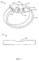
FIG. 1 is a simplified view of an example electronic device (i.e. a watch) and corresponding charging station which can each incorporate a three-dimensional inductive coil assembly in accordance with some embodiments of the invention; -
FIG. 2 is a simplified cross-sectional view of a planar inductive receiver coil disposed above a curved charging surface of an electronic device, and a simplified cross-sectional view of a corresponding planar inductive transmitter coil disposed under a curved charging surface of a charging station; -
FIG. 3 shows a multi-layered structure usable to form a three-dimensional inductive coil assembly according to some embodiments of the invention; -
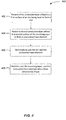
FIG. 4 is a flowchart of a method of making a three-dimensional inductive coil assembly for wireless charging according to some embodiments of the invention; -
FIG. 5A is a simplified cross-sectional view of a multi-layered coil assembly prior to molding according to some embodiments of the invention; -
FIG. 5B is a simplified cross-sectional view of another multi-layered coil assembly prior to molding according to some embodiments of the invention; -
FIG. 6A and FIG. 6B are simplified diagrams illustrating a compression molding process according to some embodiments of the invention; -
FIG. 7A and FIG. 7B are simplified diagrams illustrating a vacuum forming process according to some embodiments of the invention; -
FIG. 8A and FIG. 8B are top and bottom views of a three-dimensional inductive coil assembly according to some embodiments of the invention; -
FIG. 9 shows a wound coil that has been formed into a three-dimensional inductive coil assembly according to some embodiments of the invention; -
FIG. 10 is a simplified cross-sectional view of an example electronic device (i.e. a watch) and charging station including three-dimensional inductive coil assemblies according to some embodiments of the invention. - Some embodiments of the invention pertain to methods of making a three-dimensional inductive coil assembly configured to transmit or receive power in an electronic device or charging station. As described in further detail below, the methods can include patterning and molding a multi-layered coil structure to form a coil assembly having the desired three-dimensional shape. The described methods can provide a number of advantages over existing solutions, including enhanced coil shape control, improved precision of coil dimensions, the ability to form thinner coils occupying less space, scalability, and more efficient and low-cost manufacturing processes. Moreover, the three-dimensional shape of the formed coil assemblies can precisely conform to the contours of the charging surface of an electronic device or charging station. Such a configuration can reduce the distance between transmitter and receiver coils when an electronic device is "docked" in the charging station, thereby improving power transfer efficiency.
- Embodiments of the invention may operate with one or more inductive charging components such as electronic devices and chargers. An example is shown in
FIG. 1 . As shown, a wearable electronic device 100 (i.e. a watch) includes acasing 102 that houses adisplay 104 and various input devices including adial 106 and abutton 108. -
Device 100 may be worn on a user's wrist and secured thereto by aband 110.Band 110 includeslugs band 110 that fit within respective recesses orapertures casing 102 and allowband 110 to be removably attached tocasing 102.Lugs band 110 or may be separable (and/or separate) from the band. Generally, lugs 112a, 112b may lock intorecesses band 110 andcasing 102. Casing 102 can include electronic circuitry (not shown), including a processor, communication circuitry, and sensors that enabledevice 100 to perform a variety of functions. - A battery (not shown) internal to casing 102
powers device 100. The battery can be recharged by an external power source, anddevice 100 can include circuitry configured to operate as a receiver in a wireless power transfer system. For example, the circuitry can include a receiver coil configured for inductive charging, such that a current is generated within the coil in response to an externally applied time-varying magnetic field. The receiver coil can be disposed withincasing 102 and, in particular, above acurved charging surface 116 shown inFIG. 1 . -
FIG. 1 also shows a "charger" or chargingstation 100'.Charger 100' includes a curved charging surface 116' that is designed to conform to surface 116 ofdevice 100.Charger 100' can be connected to an external power supply through a cable (not shown), and can also include a power-transmitting component such as an inductive transmitter coil to transmit power wirelessly todevice 100. For example, whendevice 100 is docked incharger 100' withsurface 116 resting on surface 116', a transmitter coil disposed below surface 116' can generate a time-varying magnetic field (e.g., by way of AC flowing through the transmitter coil). The generated field can then induce a corresponding time-varying current in the receiver coil disposed abovesurface 116 ofdevice 100.Device 100 can utilize the generated current (e.g., by rectification into DC) to power its battery.Device 100 andcharger 100' are examples of inductive charging components. -
FIG. 2 is an expanded, simplified, cross-sectional view ofsurface 116 ofdevice 100 showing an inductivecharger receiver coil 202 disposed abovesurface 116. As shown,receiver coil 202 is a conventional flat coil. As a result of the planar geometry,coil 202 is disposed close tosurface 116 but does not precisely conform to it, thereby creating agap 204. - Also shown in
FIG. 2 is an expanded, simplified, cross-sectional view of surface 116' ofcharger 100'. Similar toreceiver coil 202,charger 100' includes a conventional flat transmitter coil 202' disposed below surface 116'. Transmitter coil 202' is disposed close to surface 116' but does not conform to surface 116' due to its planar geometry, thereby creating a gap 204'. As a result ofgaps 204, 204', there is an undesirable spacing betweencoils 202, 202' whendevice 100 is docked incharger 100', as this spacing can reduce power transfer efficiency fromcharger 100' todevice 100. - In embodiments of the present invention, methods are provided for making three-dimensional inductive coil assemblies that can better conform to the charging surfaces of electronic devices and charging stations, thereby reducing or eliminating gaps (e.g.,
gaps 204, 204') and improving charging efficiency. In some embodiments, methods can include patterning and molding a multi-layered structure to form a coil assembly having the desired geometry. -
FIG. 3 shows amulti-layered structure 300 usable to form a three-dimensional inductive coil assembly according to some embodiments of the invention. In the example shown inFIG. 3 ,structure 300 comprises a plurality of layers including a firstconductive layer 302, an insulatinglayer 306, and a secondconductive layer 310. - First
conductive layer 302 and secondconductive layer 310 can comprise any suitable electrically conductive material including, but not limited to, metals (e.g., copper, gold, silver, etc.), alloys, semiconductors, conductive ceramics, conductive polymers, and the like. Insulatinglayer 306 can comprise any suitable electrically insulating material compatible with molding processes such as the thermoforming processes described herein. For example, in some embodiments, insulating layer can comprise a polymer such as polyimide, PET, and other thermoformable materials. - As shown in
FIG. 3 , firstconductive layer 302 can be affixed to a first surface of insulatinglayer 306 by a firstadhesive layer 304 which can comprise, for example, epoxy, acrylic, or the like. Similarly, secondconductive layer 310 can be affixed to a second surface of insulatinglayer 306 by a secondadhesive layer 308 which can also comprise, for example, epoxy, polyimide, or acrylic. - Starting with
multi-layered structure 300, a number of processes can be performed in accordance with various embodiments of the present invention to form an inductive coil assembly having a three-dimensional shape. For example, as described in further detail below with regard to the method ofFIG. 4 , firstconductive layer 302 can be patterned (e.g., by etching) to form a coil configured to transmit or receive power. Secondconductive layer 310 can also be patterned to form a conductive trace element. The coil and conductive trace element can be electrically coupled by, for example, forming a via through the insulating layer. In some embodiments, the resulting structure comprising the coil, insulator layer, and trace element can then be molded into a desired three-dimensional shape using a thermoforming process such as compression molding, vacuum forming, or the like. - It should be noted that the particular configuration of
structure 300 shown inFIG. 3 is not intended to be limiting. For example, althoughstructure 300 is depicted as including one insulating layer disposed between two conductive layers, any suitable number of conductive and insulating layers can be utilized in accordance with various embodiments of the invention. -
FIG. 4 is a flowchart of amethod 400 of making a three-dimensional inductive coil assembly according to some embodiments of the invention. In some embodiments,method 400 can incorporate a multi-layered structure such asstructure 300 described above and shown inFIG. 3 . For simplicity of discussion,method 400 is described below with reference to the various layers ofstructure 300. - At
block 402, a first conductive layer (i.e. layer 302) affixed to a first surface of an insulating layer (i.e. layer 306) is patterned to form a coil configured to transmit or receive power. In some embodiments, the coil can be patterned from firstconductive layer 302 using an etching process where regions of firstconductive layer 302 are removed by a chemical etchant with the portions of firstconductive layer 302 left behind forming the coil. For example, in some embodiments, a mask that is resistant to the etchant and includes the desired coil design (e.g., a spiral) can be affixed to the surface of firstconductive layer 302 exposed to the etchant, the mask being removed at the end of the patterning process. - In some embodiments, photolithography techniques can be used to generate the mask having the desired coil design. In such processes, a layer of photoresist can be applied to first
conductive layer 302 and exposed to light (e.g., UV) in the desired geometric pattern. Upon application of a developer solution that dissolves the regions of the photoresist exposed to the light (or that dissolves the un-exposed regions), the remaining photoresist can act as the mask that forms the coil design in firstconductive layer 302 after etching. - Any suitable etchant can be used in embodiments of the invention so long as the selected etchant dissolves the exposed regions of first
conductive layer 302 but does not dissolve (or dissolves at a slower rate) the mask material. Suitable etchants can include, but are not limited to, hydrofluoric acid, phosphoric acid, hydrochloric acid, nitric acid, sodium hydroxide, SC-1 solution, organic solvents, plasma etchants, and the like. Coils having very intricate patterns can be precisely formed according to embodiments of the present invention. - In some other embodiments, first
conductive layer 302 can be printed or otherwise deposited onto insulatinglayer 306 in the desired coil pattern using known printing or deposition techniques. Depending on the feature size required for the coil, solid ink printers can be used to print the coil and/or to print the mask prior to etching. - At
block 404, a second conductive layer (i.e. layer 310) affixed to a second surface of insulatinglayer 306 opposite the first surface is patterned to form a conductive trace element. As with the coil patterned atblock 404, the conductive trace element can be patterned from secondconductive layer 310 using an etching process where regions of secondconductive layer 310 are removed by a chemical etchant with the portions of secondconductive layer 310 left behind forming the conductive trace element. For example, in some embodiments, a mask that is resistant to the etchant and includes the desired trace element design (e.g., a flat wire) can be affixed to the surface of secondconductive layer 310 exposed to the etchant, the mask being removed at the end of the patterning process. - In some embodiments, photolithography techniques can be used to generate the mask having the desired trace element design. In such processes, a layer of photoresist can be applied to second
conductive layer 310 and exposed to light (e.g., UV) in the desired geometric pattern. Upon application of a developer solution that dissolves the regions of the photoresist exposed to the light (or dissolves the un-exposed regions), the remaining photoresist can act as the mask that leaves behind the conductive trace element in secondconductive layer 310 after etching. - Any suitable etchant can be used in embodiments of the invention so long as the selected etchant dissolves the exposed regions of second
conductive layer 310 but does not dissolve (or dissolves at a slower rate) the mask material. Suitable etchants can include, but are not limited to, hydrofluoric acid, phosphoric acid, hydrochloric acid, nitric acid, sodium hydroxide, SC-1 solution, organic solvents, plasma etchants, and the like. In some other embodiments, secondconductive layer 310 can be printed or otherwise deposited onto insulatinglayer 306 in the desired pattern using known printing or deposition techniques. - At
block 406, the coil formed from patterning firstconductive layer 302, and the conductive trace element formed from patterning secondconductive layer 310 can be electrically coupled. In some embodiments, this coupling can be achieved by way of a via that extends through insulatinglayer 306, and throughadhesive layers conductive layer 302, and secondconductive layer 310 can be the same material (e.g., copper). - Additional processing can be performed on the multi-layered structure formed at blocks 402-406. In some embodiments,
method 400 can further include laminating the coil and an exposed region of the first surface of insulatinglayer 306. In further embodiments,method 400 can further include depositing a ferromagnetic layer onto the conductive trace element and an exposed region of the second surface of insulatinglayer 306. In some other embodiments, the ferromagnetic layer can be deposited onto the coil and the exposed region of the first surface of insulatinglayer 306, and laminating can be performed on the conductive trace element and the exposed region of the second surface of insulatinglayer 306. The ferromagnetic material can comprise ferrite (i.e. a material comprising Fe2O3) in some embodiments. The laminate can comprise any suitable electrically insulating material including, for example, an epoxy resin, in some embodiments. -
FIG. 5A is a simplified cross-sectional view of amulti-layered coil assembly 500 prior to molding (i.e. prior to block 408 of method 400) according to some embodiments of the invention. As shown inFIG. 5A ,assembly 500 can includelaminate layer 502, patternedcoil 504, insulatinglayer 306,conductive trace element 508, andferromagnetic layer 510. In some embodiments, adhesive layers (e.g., layers 304, 308 inFIG. 3 ) may be present betweenpatterned coil 504 and insulatinglayer 306 and between insulatinglayer 306 andconductive trace element 508.Laminate layer 502 can serve the function of electrically insulating the final coil assembly from nearby components or metallic surfaces of an electronic device or charging station in which the coil assembly is installed.Ferromagnetic layer 510 can serve the function of containing and concentrating magnetic fields within the coil assembly during wireless charging, thereby improving the efficiency of power transfer. In some embodiments,ferromagnetic layer 510 can comprise a composite of polymer and ferrite characterized by a ductility suitable for thermoforming processes. The polymer, such as an acrylic polymer in some embodiments, may act as a binder for small ferrite particles. Such a composite may be designed to not crack during subsequent thermoforming processes due to its ductility at high temperatures. -
FIG. 5B is a simplified cross sectional view ofmulti-layered coil assembly 550 prior to molding according to some embodiments of the invention. As shown inFIG. 5B ,assembly 550 can include more than one patterned coil.Assembly 550 can includelaminate layer 502, patternedcoil 504, insulatinglayer 306, a second patterned coil 505, a second insulatinglayer 306,conductive trace element 508, andferromagnetic layer 510. In some embodiments, patterned coil 505 can be patterned differently from patternedcoil 504. In some embodiments, an insulating layer between second patterned coil 505 andconductive trace element 508 can be made of a different material from the insulating layer between firstpatterned coil 504 and second patterned coil 505. Althoughassembly 550 includes two patterned coil layers, other embodiments can include three or more patterned coil layers separated by insulating layers. - In some other embodiments, not shown in
FIGS. 5A-5B ,laminate layer 502 andferromagnetic layer 510 can be added toassembly 500 afterblock 408 inFIG. 4 . For example, whenlaminate layer 502 and/orferromagnetic layer 510 are not ductile enough for thermoforming processes, one or both of these layers can be applied in one or more separate processes. - At
block 408,assembly 500 can be subjected to a molding process to form a three-dimensional shape. In some embodiments, the assembly that is molded comprises patternedcoil 504, insulatinglayer 306, andconductive trace element 508. In some embodiments, as shown inFIGS. 5A-5B , the assembly that is molded further compriseslaminate layer 502 andferromagnetic layer 510. In some embodiments, atblock 408, the assembly can be molded into the three-dimensional shape by way of a thermoforming process where pressure and heat are applied simultaneously. Exemplary thermoforming processes are described in further detail below with reference toFIGS. 6A-7B . -
FIGS. 6A and 6B are simplified diagrams illustrating a compression molding process according to some embodiments of the invention. InFIGS. 6A-6B , the compression molding process is illustrated in two parts, 600a, 600b for simplicity of discussion. As shown inFIG. 6A ,multi-layered coil assembly 500 fromFIG. 5A is placed on amold 604.Mold 604 can have a cavity having a shape that corresponds to the final three-dimensional target shape ofcoil assembly 500. InFIG. 6A , this target shape has a concave bowl-like geometry. In other embodiments, the cavity shape ofmold 604 can correspond to any other suitable geometry designed to conform to the contours of a charging surface of an electronic device or charging station. - In some embodiments, the cavity shape of
mold 604 can be slightly different than the final target shape ofcoil assembly 500 to account for elastic deformation. In such embodiments, the cavity shape ofmold 604 can be calculated to account for "spring-back" effects after molding. By taking such factors into account, the final three-dimensional shape ofcoil assembly 500 can precisely conform to a charging surface of the intended electronic device or charging station. - As shown
FIG. 6A , aplug member 602 can have a shape that corresponds to the shape of the cavity ofmold 604. For example, in this non-limiting illustration,plug member 602 has a convex shape that corresponds to the concave shape of the cavity ofmold 604. Appropriate force can be applied through the movement ofplug member 602 towards the cavity of mold 604 (or vice versa), thereby contacting and deformingcoil assembly 500 in the process. As force (i.e. pressure) is applied, aheating element 606 can provide the appropriate temperature to softencoil assembly 500 thereby improving the ductility of the constituent layers. For example, heating can be provided through infra-red (IR) heating, radio frequency (RF) heating, hot air heating, and the like. In some embodiments, the heat and pressure can be maintained until insulating layer 306 (e.g., polyimide) has cured. In some embodiments, a temperature of 100-250 °C can be used. The length of time during which heat and pressure are applied can vary depending on, for example, the shape and size ofcoil assembly 500. -
FIG. 6B showscoil assembly 500 inmold 604 after heat and pressure have been applied. As seen inFIG. 6B ,coil assembly 500 can take the shape of the space betweenmold 604 and plugmember 602. In some embodiments,coil assembly 500, in this shape, can conform to a charging surface of an electronic device or charging station and can represent the final shape of the coil assembly. In some other embodiments, the shape ofcoil assembly 500 may change upon removing of the pressure and/or cooling, owing to a spring-back effect. In such embodiments, the shape of the coil assembly after spring-back may conform to the desired charging surface. - At the end of molding, and after cooling, the final multi-layered coil assembly having the three-dimensional shape may be rigid. According to some embodiments, a trimming or cutting of excess material can be performed prior to installing the coil assembly of the desired shape and dimensions in an electronic device or charging station.
-
FIGS. 7A and 7B are simplified diagrams illustrating a vacuum forming process according to some embodiments of the invention. InFIGS. 7A-7B , the vacuum forming process is illustrated in two parts, 700a, 700b for simplicity of discussion. As shown inFIG. 7A ,multi-layered coil assembly 500 fromFIG. 5A is placed on amold 702.Mold 702 can have a cavity characterized by a shape that corresponds to the final three-dimensional target shape ofcoil assembly 500. InFIG. 7A , this target shape has a concave bowl-like geometry. In other embodiments, the cavity shape ofmold 702 can correspond to any other suitable geometry designed to conform to the contours of a charging surface of an electronic device or charging station. - In some embodiments, the cavity shape of
mold 702 can be slightly different than the final target shape ofcoil assembly 500 to account for elastic deformation. In such embodiments, the cavity shape ofmold 702 can be calculated to account for "spring-back" effects after molding. By taking such factors into account, the final three-dimensional shape ofcoil assembly 500 can precisely conform to a charging surface of the intended electronic device or charging station. - As shown
FIG. 7A , pressure is applied tocoil assembly 500 by means of a vacuum throughoutlet 704 inmold 702. In evacuating the air from acavity region 708, the air pressure insidecavity region 708 becomes lower than the pressure outside cavity region 708 (i.e. on the upper surface pf coil assembly 500). This results in a suction force that "pulls"coil assembly 500 towards the cavity surface ofmold 702. As the vacuum is applied, aheating element 706 can provide the appropriate temperature to softencoil assembly 500 thereby improving the ductility of the constituent layers. For example, heating can be provided through infra-red (IR) heating, radio frequency (RF) heating, hot air heating, and the like. In some embodiments, the heat and pressure can be maintained until insulating layer 306 (e.g., polyimide) has cured. In some embodiments, a temperature of 100-250 °C can be used. The length of time during which heat and pressure are applied can vary depending on, for example, the shape and size ofcoil assembly 500. - The vacuum forming process shown in
FIGS. 7A-7B for forming the three-dimensional shape ofcoil assembly 500 can provide several advantages. For example, in the vacuum forming process, no force need be directly applied to the top surface ofcoil assembly 500. Such a configuration can minimize cracks or fractures otherwise caused by contact forces (i.e. from a plug member) during molding. -
FIG. 7B showscoil assembly 500 inmold 702 after heat and pressure have been applied. As seen inFIG. 7B ,coil assembly 500 can take the shape ofmold 702. In some embodiments,coil assembly 500, in this shape, can conform to a charging surface of an electronic device or charging station and can represent the final shape of the coil assembly. In some other embodiments, the shape ofcoil assembly 500 may change upon removing the vacuum and/or cooling, owing to a spring-back effect. In such embodiments, the shape of the final coil assembly after spring-back may conform to the desired charging surface. - At the end of molding, and after cooling, the final multi-layered coil assembly having the three-dimensional shape may be rigid. According to some embodiments, a trimming or cutting of excess material can be performed prior to introducing the coil assembly of the desired shape and dimensions into an electronic device or charging station.
- Although the layers of
coil assembly 500 are depicted inFIGS. 6A-7B as being molded simultaneously, in some embodiments, one or more layers ofcoil assembly 500 can be formed and molded separately. Each layer can be molded using any suitable process described herein such as, for example, a compression molding and/or vacuum forming process. Separately molded layers having a three-dimensional shape may be assembled (e.g., using an adhesive) to form the final multi-layered coil assembly characterized by the three-dimensional shape. -
FIGS. 8A and 8B are top andbottom views FIGS. 8A-8B can be formed in accordance with the methods described herein (i.e. method 400) and using any suitable molding process such as compression molding (as shown inFIGS. 6A-6B ), vacuum forming (as shown inFIGS. 7A-7B ), or other suitable molding process. In other words,FIGS. 8A and 8B illustrate the result of forming and thermoformingmulti-layered coil assembly 500 in some embodiments. - As seen in
FIG. 8A , apatterned coil 802 is disposed on insulatinglayer 804 and has a three-dimensional helical shape. In some embodiments, patternedcoil 802 may be coated or otherwise covered with a ferromagnetic (e.g., ferrite) layer (not shown inFIG. 8A ). The coil assembly also includes aconductive trace element 806 on the opposite surface of insulatinglayer 804.Patterned coil 802 can include anend 810 that is electrically coupled totrace element 806 by, for example, a via that extends through insulatinglayer 804.Conductive trace element 806 can be electrically coupled to awire 808a, andpatterned coil 802 can be electrically coupled to awire 808b. - If the coil assembly is a transmitter (e.g., in a charging station), time-varying electrical current can flow through
wire 808a,trace element 806, patternedcoil 802, andwire 808b, to generate a time-varying magnetic field. If the coil assembly is a receiver (e.g., in an electronic device), a time-varying magnetic field generated by a proximate transmitter coil can induce a current that flows throughwire 808a,trace element 806, patternedcoil 802, andwire 808b, the induced current being usable to charge a battery. - In the
top view 800b of the coil assembly shown inFIG. 8B , the coil assembly further includes alaminate layer 812 under whichconductive trace element 806 is disposed. As further shown inFIG. 8B , an outline of patternedcoil 802 can also be seen throughlaminate layer 812 as a result of the molding process deforming insulatinglayer 804. - In some embodiments, instead of patterning and molding
multi-layered structure 300 described above, a wound coil can be used as a starting structure and then molded into the desired three-dimensional shape by way of, for example, the thermoforming processed described above with regard toFIGS. 6A-7B . Use of wound coils in place of a multi-layered structure can provide advantages in a wireless power transfer system. For example, the dimensions of a wound coil and the amount of conductive material contained therein can be greater than that of a coil formed by the patterning techniques described herein. This can provide for lower impedance at target AC frequencies and increased inductance. The quality factor (Q) of the coil, which is a measure of efficiency, is thereby increased as it represents the ratio of inductive reactance to coil resistance at a selected frequency. - In some embodiments, an insulated metal (e.g., copper) wire can be mechanically wound into the desired spiral shape to form the coil. For example, the wire can be wound about an object having a circular cross section such a solid or hollow tube. The shape of the wound coil can be fixed by way of a suitable bonding material. In some embodiments, the insulator on the wire comprises an epoxy resin such as polyurethane or a polyester compound. A bonding agent such as polyimide, a rubber, nitrile or other heat-sensitive material can also be used. Upon heating the wound coil to a critical temperature determined by the selected organic materials, the wound insulated wire can be bonded into place to form a "resin-potted" wound coil. In some embodiments, the wound coil can have a planar geometry. The wound coil can then be molded into the desired three-dimensional shape using any suitable molding process including, for example, the thermoforming processes described above with respect to
FIGS. 6A-7B . -
FIG. 9 shows a wound coil that has been formed into a three-dimensionalinductive coil assembly 900 according to some embodiments of the invention. As shown inFIG. 9 ,assembly 900 comprises thewound coil 904 having a plurality of windings of insulated wire. The wire inwound coil 904 can comprise any suitable conductive metal such as copper, gold, silver, or the like. In some other embodiments, the wire can comprise another type of conductive material such as an alloy, semiconductor, conductive ceramic, conductive polymer, or the like. - As further shown in
FIG. 9 , woundcoil 904 can be bonded in a resin. The resin can comprise polyurethane, polyester, or other suitable resin, and can further comprise a bonding agent such as a polyimide, rubber, nitrile, or the like. Aconductive trace element 902 can be electrically coupled to the "beginning" and "end" ofwound coil 904 to allow electrical current from a power source to flow throughwound coil 904.Assembly 900, as shown inFIG. 9 , has been molded into a three-dimensional shape using a thermoforming process such as compression molding (FIGS. 6A-6B ), vacuum forming (FIGS. 7A-7B ), or other suitable molding process. -
FIG. 10 is a simplified cross-sectional view of an example electronic device 1000 (i.e. a watch) and charging station 1000' including three-dimensional inductive coil assemblies according to some embodiments of the invention.Electronic device 1000 and charging station 1000' are examples of inductive charging components. As shown inFIG. 10 , areceiver coil assembly 1004, formed according to embodiments of the invention, may be disposed adjacent to a non-planar (e.g., curved) chargingsurface 1002 ofdevice 1000. In some embodiments,receiver coil assembly 1004 may be attached tosurface 1002 by means of a pressure sensitive adhesive (PSA). The PSA can form a bond between the surface and the coil assembly when pressure is applied, without the need for a solvent, heat, or water to activate the PSA.Device 1000 can further include circuitry (not shown) configured to utilize current generated inreceiver coil assembly 1004 to charge a battery. - Likewise, charging station 1000' can comprise a corresponding transmitter coil assembly 1004' formed according to embodiments of the invention. Transmitter coil assembly 1004' may be disposed adjacent to a non-planar (e.g., curved) charging surface 1002' of charging station 1000'. As seen in
FIG. 10 , charging surface 1002' may be contoured to conform to chargingsurface 1002 ofdevice 1000 whendevice 1000 is docked in charging station 1000'. In some embodiments, transmitter coil assembly 1004' may also be attached to charging surface 1002' by means of a pressure sensitive adhesive (PSA). Charging station 1000' may be connected to a source of power through apower input 1006. The power source for the charging station 1000' can be a replaceable battery, rechargeable battery, external power supply, or the like. Charging station 1000' can further include circuitry (not shown) configured to generate time-varying current (e.g., AC) in transmitter coil assembly 1004' for wireless power transfer todevice 1000. - In some embodiments,
coil assemblies 1004 and 1004' can be identical. In some other embodiments,coil assemblies 1004 and 1004' can have different coil dimensions, numbers of windings, numbers of layers, etc. For example, transmitter coil assembly 1004' can have a greater number of turnings and/or thicker wire, and thus effectively more metal. Such a configuration can account for ohmic and other losses that may occur during wireless power transmission. In some embodiments where a wound coil such ascoil 900 is used for the transmitter and receiver coil assemblies, the diameter of the transmitter coil can be greater than the diameter of the receiver coil. - During a charging operation, power may be transferred wirelessly from transmitter coil assembly 1004' to
receiver coil assembly 1004. During such an operation,device 1000 can be docked in charging station 1000' with chargingsurfaces 1002 and 1002' adjacent to each other. In such a configuration, transmitter coil assembly 1004' may be aligned withreceiver coil assembly 1004 along a shared axis in some embodiments. - The patterned coil of transmitter coil assembly 1004' can produce a time-varying electromagnetic flux to induce a current within the patterned coil of
receiver coil assembly 1004. The patterned coil transmitter coil assembly 1004' may transmit power at a selected frequency or band of frequencies. In some embodiments, the transmit frequency is substantially fixed, although this is not required. For example, the transmit frequency may be adjusted to improve power transfer efficiency for particular operational conditions. More particularly, a high transmit frequency may be selected if more power is required bydevice 1000 and a low transmit frequency may be selected if less power is required. In some other embodiments, patterned coil of transmitter coil assembly 1004' may produce a static electromagnetic field and may physically move, shift, or otherwise change its position to produce a spatially-varying electromagnetic flux to induce a current within the patterned coil ofreceiver coil assembly 1004. - As shown in
FIG. 10 , the patterned coils of transmitter coil assembly 1004' andreceiver coil assembly 1004 are disposed close together with very little or no gap between the coils and the surfaces. This arrangement can reduce leakage flux, thereby minimizing loss during transfer of power, improving charging efficiency, and allowing for faster charging. -
Device 1000 may include a processor (not shown) that can be used to control the operation of or coordinate one or more functions of charging station 1000'. In some embodiments, charging station 1000' may include one or more sensors to determine whetherdevice 1000 is present and ready to receive power from charging station 1000'. For example, charging station 1000' may include an optical sensor, such as an infrared proximity sensor. When charging station 1000' is attached to or brought within the proximity ofdevice 1000, the infrared proximity sensor may produce a signal that the processor indevice 1000 may use to determine the presence of charging station 1000'. Examples of other sensors that may be suitable to detect or verify the presence ofdevice 1000 may include a mass sensor, a mechanical interlock, switch, button or the like, a Hall effect sensor, or other electronic sensor. - As previously mentioned, although embodiments described in the drawings and specification relate to coil assemblies as used in a personal wearable electronic devices such as a watch, embodiments of the invention can be used in a variety of wearable or non-wearable electronic devices in addition to the particular wrist-worn electronic devices discussed above. For example, embodiments of the invention may be used in Bluetooth headsets, smartphones, electronic glasses, wearable medical devices, and wearable fitness devices.
- The foregoing description, for purposes of explanation, used specific nomenclature to provide a thorough understanding of the described embodiments. However, it will be apparent to one skilled in the art that the specific details are not required in order to practice the described embodiments. For example, while several specific embodiments of the invention described above use inductive coupling to wireless transmit power to a wearable electronic device, the invention is not limited to any particular wireless power transfer technique and other near-field or non-radiative wireless power transfer techniques as well as radiative wireless power transfer techniques can be used in some embodiments. Thus, the foregoing descriptions of the specific embodiments described herein are presented for purposes of illustration and description. They are not target to be exhaustive or to limit the embodiments to the precise forms disclosed. It will be apparent to one of ordinary skill in the art that many modifications and variations are possible in view of the above teachings.
Claims (15)
- An inductive coil assembly for wireless charging, comprising:an insulating layer comprising a first surface and a second surface opposite the first surface;a first conductive layer affixed to the first surface of the insulating layer and patterned to form a coil configured to transmit or receive power;a second conductive layer affixed to the second surface of the insulating layer and patterned to form a conductive trace element, wherein the coil and the conductive trace element are electrically coupled.
- The coil assembly of claim 1 wherein the first conductive layer, the insulating layer, and the second conductive layer are characterized by a three-dimensional shape.
- The coil assembly of claim 1 wherein the coil and the conductive trace element are electrically coupled by a via formed through the insulating layer.
- The coil assembly of claim 2 further comprising a laminate layer disposed on the first conductive layer, wherein the laminate layer is characterized by the three-dimensional shape.
- The coil assembly of claim 2 further comprising a ferrite layer disposed on the second conductive layer, wherein the ferrite layer is characterized by the three-dimensional shape.
- The coil assembly of claim 1 wherein the first conductive layer and the second conductive layer independently comprise a metal, and wherein the insulating layer comprises a polymer.
- The coil assembly of claim 1 wherein the first conductive layer is adhesively coupled to the first surface of the insulating layer, and wherein the second conductive layer is adhesively coupled to the second surface of the insulating layer.
- A method of making a three-dimensional inductive coil assembly for wireless charging comprising:patterning a first conductive layer affixed to a first surface of an insulating layer to form a coil configured to transmit or receive power;patterning a second conductive layer affixed to a second surface of the insulating layer opposite the first surface to form a conductive trace element;electrically coupling the coil and the conductive trace element; andmolding the coil, the insulating layer, and the conductive trace element into a three-dimensional shape.
- The method of claim 8 wherein the coil, the insulating layer, and the conductive trace element are molded simultaneously.
- The method of claim 8 wherein patterning the first conductive layer comprises etching the first conductive layer to form the coil.
- The method of claim 8 wherein patterning the second conductive layer comprises etching the second conductive layer to form the conductive trace element.
- The method of claim 8 wherein electrically coupling the coil and the conductive trace element comprises forming a via through the insulating layer.
- The method of claim 8, further comprising:laminating the coil and an exposed region of the first surface of the insulating layer prior to molding.
- The method of claim 8, further comprising:depositing a ferrite layer onto the conductive trace element and an exposed region of the second surface of the insulating layer prior to molding.
- The method of claim 8 wherein the first conductive layer is adhesively coupled to the first surface of the insulating layer, and wherein the second conductive layer is adhesively coupled to the second surface of the insulating layer.
Applications Claiming Priority (2)
| Application Number | Priority Date | Filing Date | Title |
|---|---|---|---|
| US201562208451P | 2015-08-21 | 2015-08-21 | |
| US15/082,935 US10211663B2 (en) | 2015-08-21 | 2016-03-28 | 3D shaped inductive charging coil and method of making the same |
Publications (2)
| Publication Number | Publication Date |
|---|---|
| EP3133617A1 true EP3133617A1 (en) | 2017-02-22 |
| EP3133617B1 EP3133617B1 (en) | 2021-05-12 |
Family
ID=56561208
Family Applications (1)
| Application Number | Title | Priority Date | Filing Date |
|---|---|---|---|
| EP16178031.7A Active EP3133617B1 (en) | 2015-08-21 | 2016-07-05 | 3d shaped inductive charging coil and method of making the same |
Country Status (3)
| Country | Link |
|---|---|
| US (1) | US10211663B2 (en) |
| EP (1) | EP3133617B1 (en) |
| CN (2) | CN106469945A (en) |
Cited By (2)
| Publication number | Priority date | Publication date | Assignee | Title |
|---|---|---|---|---|
| EP3637443A1 (en) * | 2018-10-10 | 2020-04-15 | Nokia Technologies Oy | Inductive components and methods of forming inductive components |
| CN118567238A (en) * | 2024-08-01 | 2024-08-30 | 中铁电气化局集团有限公司 | Flexible bus prefabrication construction method and system based on intelligent control system |
Families Citing this family (26)
| Publication number | Priority date | Publication date | Assignee | Title |
|---|---|---|---|---|
| US10056850B2 (en) * | 2015-10-12 | 2018-08-21 | Joseph L. Meloche | Wearable power generating device |
| CN106899090A (en) * | 2017-03-17 | 2017-06-27 | 宁波微鹅电子科技有限公司 | Wireless power component and electronic installation |
| US11605487B2 (en) * | 2017-04-14 | 2023-03-14 | The Diller Corporation | Laminate with induction coils and charging station device comprising same |
| CN108492976B (en) * | 2018-03-13 | 2021-05-07 | 上海威斯科电子材料有限公司 | Coil structure and preparation method of composite coil structure |
| US12471217B2 (en) | 2019-05-02 | 2025-11-11 | Nano Dimension Technologies, Ltd. | Systems and methods of fabricating coils for coreless transformers and inductors |
| TWI849118B (en) * | 2019-05-02 | 2024-07-21 | 以色列商納米尺寸技術領域股份有限公司 | Systems and methods of fabricating coils for coreless transformers and inductors |
| CN110277646B (en) * | 2019-05-28 | 2021-03-05 | 超级智慧家(上海)物联网科技有限公司 | Wireless charging stereo antenna for electronic equipment |
| US11967450B2 (en) | 2019-09-23 | 2024-04-23 | Apple Inc. | Plastic back crystal window with insert-molded planar coil |
| US11757307B2 (en) | 2020-01-03 | 2023-09-12 | Nucurrent, Inc. | Systems and methods for dynamically tuning a wireless power transfer system |
| CN111862809B (en) * | 2020-06-30 | 2022-07-12 | 上海中航光电子有限公司 | Display device and vehicle |
| US11303165B2 (en) | 2020-07-24 | 2022-04-12 | Nucurrent, Inc. | Low cost communications demodulation for wireless power receiver system |
| US11303164B2 (en) | 2020-07-24 | 2022-04-12 | Nucurrent, Inc. | Low cost communications demodulation for wireless power transmission system |
| CN112002526B (en) * | 2020-09-02 | 2021-06-29 | 南方电网电力科技股份有限公司 | A high-voltage wireless power transmission coil |
| US11646606B2 (en) | 2021-01-22 | 2023-05-09 | Microsoft Technology Licensing, Llc | Receive and transmit coil pair selection |
| US11271611B1 (en) | 2021-01-28 | 2022-03-08 | Nucurrent, Inc. | Wireless power transfer with in-band virtualized wired communications |
| US11483033B2 (en) | 2021-01-28 | 2022-10-25 | Nucurrent, Inc. | Wireless power transfer system with data versus power priority optimization |
| CN112967879B (en) * | 2021-02-01 | 2022-12-06 | 新昌县新明实业有限公司 | A process for forming and processing transformer insulating material electric porcelain |
| US11527912B2 (en) * | 2021-02-01 | 2022-12-13 | Nucurrent, Inc. | Shaped coil for wireless power transmission system coupling |
| US11811244B2 (en) | 2021-02-01 | 2023-11-07 | Nucurrent, Inc. | Automatic gain control for communications demodulation in wireless power transmitters |
| US11289952B1 (en) | 2021-02-10 | 2022-03-29 | Nucurrent, Inc. | Slotted communications in virtual AC power signal transfer with variable slot width |
| US11532956B2 (en) | 2021-04-30 | 2022-12-20 | Nucurrent, Inc. | Power capability detection with verification load in power level control systems for wireless power transmission |
| US11539247B2 (en) | 2021-04-30 | 2022-12-27 | Nucurrent, Inc. | Power capability detection in precision power level control systems for wireless power transmission |
| US11637448B1 (en) | 2021-10-12 | 2023-04-25 | Nucurrent, Inc. | Wireless power transmitter with removable magnetic connector panel for vehicular use |
| CN114311617A (en) * | 2021-12-21 | 2022-04-12 | 昆山联滔电子有限公司 | Coil assembly, manufacturing method and manufacturing equipment thereof, and earphone device |
| US12573883B2 (en) | 2022-09-13 | 2026-03-10 | Nucurrent, Inc. | Bit inversion for thermal mitigation in wireless power and data transfer system |
| US12476492B2 (en) | 2022-09-13 | 2025-11-18 | Nucurrent, Inc. | Bit stuffing for thermal mitigation in wireless power and data transfer system |
Citations (4)
| Publication number | Priority date | Publication date | Assignee | Title |
|---|---|---|---|---|
| JP2011072115A (en) * | 2009-09-25 | 2011-04-07 | Panasonic Electric Works Co Ltd | Noncontact charging system |
| JP2011109546A (en) * | 2009-11-19 | 2011-06-02 | Nissha Printing Co Ltd | Method of manufacturing power receiving system housing in wireless charging system |
| JP2011216621A (en) * | 2010-03-31 | 2011-10-27 | Nissha Printing Co Ltd | Coil for non-contact charging, film with the coil, molding with the coil, electronic apparatus with the coil, and method of manufacturing the molding with the coil |
| EP2645385A2 (en) * | 2012-03-29 | 2013-10-02 | Samsung Electro-Mechanics Co., Ltd | Thin film coil and electronic device having the same |
Family Cites Families (23)
| Publication number | Priority date | Publication date | Assignee | Title |
|---|---|---|---|---|
| US3731005A (en) * | 1971-05-18 | 1973-05-01 | Metalized Ceramics Corp | Laminated coil |
| US5363080A (en) * | 1991-12-27 | 1994-11-08 | Avx Corporation | High accuracy surface mount inductor |
| JP3102125B2 (en) * | 1992-02-28 | 2000-10-23 | 富士電機株式会社 | Thin film magnetic element |
| US5437091A (en) | 1993-06-28 | 1995-08-01 | Honeywell Inc. | High curvature antenna forming process |
| JP3851320B2 (en) * | 2004-03-25 | 2006-11-29 | Tdk株式会社 | Circuit device and manufacturing method thereof |
| US7271585B2 (en) * | 2004-12-01 | 2007-09-18 | Simmonds Precision Products, Inc. | Method of fabricating a multilayer wiring board proximity sensor |
| US20110050164A1 (en) * | 2008-05-07 | 2011-03-03 | Afshin Partovi | System and methods for inductive charging, and improvements and uses thereof |
| US7902826B2 (en) | 2008-12-12 | 2011-03-08 | General Electric Company | Transverse gradient coil for MRI systems and method for manufacturing the same |
| WO2010104569A1 (en) * | 2009-03-09 | 2010-09-16 | Neurds Inc. | System and method for wireless power transfer in implantable medical devices |
| EP2433347B1 (en) * | 2009-05-20 | 2013-10-23 | Koninklijke Philips N.V. | Electronic device having an inductive receiver coil with ultra-thin shielding layer and method |
| US8646695B2 (en) | 2010-10-01 | 2014-02-11 | Disney Enterprises, Inc. | Combined HF and UHF RFID device |
| US8857983B2 (en) * | 2012-01-26 | 2014-10-14 | Johnson & Johnson Vision Care, Inc. | Ophthalmic lens assembly having an integrated antenna structure |
| US9009951B2 (en) * | 2012-04-24 | 2015-04-21 | Cyntec Co., Ltd. | Method of fabricating an electromagnetic component |
| KR20140081356A (en) | 2012-12-21 | 2014-07-01 | 삼성전기주식회사 | Electromagnetic induction module for wireless charging element and manufacturing method of the same |
| KR101852940B1 (en) * | 2013-06-20 | 2018-04-27 | 엘지이노텍 주식회사 | Receiving antennas and wireless power receiving apparatus comprising the same |
| US9240375B2 (en) * | 2013-06-28 | 2016-01-19 | Stmicroelectronics, Inc. | Modular fuses and antifuses for integrated circuits |
| US9479007B1 (en) * | 2014-02-21 | 2016-10-25 | Apple Inc. | Induction charging system |
| US10447079B2 (en) * | 2014-04-18 | 2019-10-15 | Apple Inc. | Multi-coil induction |
| US9449754B2 (en) * | 2014-05-30 | 2016-09-20 | Apple Inc. | Coil constructions for improved inductive energy transfer |
| US20160064137A1 (en) * | 2014-09-02 | 2016-03-03 | Apple Inc. | Capacitively balanced inductive charging coil |
| WO2016094140A1 (en) * | 2014-12-10 | 2016-06-16 | Suzhou Qing Xin Fang Electronics Technology Co., Ltd. | Methods and devices of laminated integrations of semiconductor chips, magnetics, and capacitance |
| TWI616908B (en) * | 2015-06-16 | 2018-03-01 | 蘋果公司 | Wireless charging station |
| US9460996B1 (en) * | 2015-08-05 | 2016-10-04 | Globalfoundries Inc. | Integrated device with inductive and capacitive portions and fabrication methods |
-
2016
- 2016-03-28 US US15/082,935 patent/US10211663B2/en active Active
- 2016-07-05 EP EP16178031.7A patent/EP3133617B1/en active Active
- 2016-08-19 CN CN201610694505.1A patent/CN106469945A/en active Pending
- 2016-08-19 CN CN201620911956.1U patent/CN205945251U/en active Active
Patent Citations (4)
| Publication number | Priority date | Publication date | Assignee | Title |
|---|---|---|---|---|
| JP2011072115A (en) * | 2009-09-25 | 2011-04-07 | Panasonic Electric Works Co Ltd | Noncontact charging system |
| JP2011109546A (en) * | 2009-11-19 | 2011-06-02 | Nissha Printing Co Ltd | Method of manufacturing power receiving system housing in wireless charging system |
| JP2011216621A (en) * | 2010-03-31 | 2011-10-27 | Nissha Printing Co Ltd | Coil for non-contact charging, film with the coil, molding with the coil, electronic apparatus with the coil, and method of manufacturing the molding with the coil |
| EP2645385A2 (en) * | 2012-03-29 | 2013-10-02 | Samsung Electro-Mechanics Co., Ltd | Thin film coil and electronic device having the same |
Cited By (3)
| Publication number | Priority date | Publication date | Assignee | Title |
|---|---|---|---|---|
| EP3637443A1 (en) * | 2018-10-10 | 2020-04-15 | Nokia Technologies Oy | Inductive components and methods of forming inductive components |
| WO2020074779A1 (en) * | 2018-10-10 | 2020-04-16 | Nokia Technologies Oy | Inductive components and methods of forming inductive components |
| CN118567238A (en) * | 2024-08-01 | 2024-08-30 | 中铁电气化局集团有限公司 | Flexible bus prefabrication construction method and system based on intelligent control system |
Also Published As
| Publication number | Publication date |
|---|---|
| EP3133617B1 (en) | 2021-05-12 |
| CN205945251U (en) | 2017-02-08 |
| US20170054318A1 (en) | 2017-02-23 |
| US10211663B2 (en) | 2019-02-19 |
| CN106469945A (en) | 2017-03-01 |
Similar Documents
| Publication | Publication Date | Title |
|---|---|---|
| EP3133617B1 (en) | 3d shaped inductive charging coil and method of making the same | |
| CN104638778B (en) | Wireless power receiver and its manufacture method | |
| US20180330867A1 (en) | Methods for forming shield materials onto inductive coils | |
| US9825482B2 (en) | Electromagnetic booster for wireless charging and method of manufacturing the same | |
| US10062492B2 (en) | Induction coil having a conductive winding formed on a surface of a molded substrate | |
| US10644754B2 (en) | Wirelessly charged devices | |
| US10553345B2 (en) | Coil device and apparatus including the same | |
| US20140320369A1 (en) | Shielding layer for a device having a plurality of antennas | |
| US10574089B2 (en) | Attractor for PMA wireless charging type wireless power reception module and manufacturing method therefor, and wireless power reception module having same | |
| CN108511398B (en) | Near field communication loop and method of forming the same | |
| CN106099312A (en) | Antenna module | |
| US20190252768A1 (en) | Antenna module and electronic device having the same | |
| CN106688159B (en) | Wireless charging of metal back electronic devices | |
| JP2008288370A (en) | Surface mounting inductor, and manufacturing method thereof | |
| WO2017038797A1 (en) | Flexible printed wiring board and non-contact charge system | |
| KR20140076994A (en) | Wireless power receiver and method of manufacturing the same | |
| CN109088162B (en) | Radiating and radiating dual-purpose wireless communication antenna structure | |
| CN105321684A (en) | Magnetic core and coil device | |
| CN105743191B (en) | Wireless charging device and preparation method thereof based on MEMS micro Process planar coil | |
| KR20140053644A (en) | Method for improving the induced electromotive force by relatively increasing thickness of cu foil in pcb of wireless charger | |
| KR102029726B1 (en) | Coil type unit for wireless power transmission and manufacturing method of coil type unit for wireless power transmission | |
| JP6231061B2 (en) | Receiving coil unit of non-contact power feeding device and manufacturing method thereof | |
| CN110164678A (en) | Magnetic flexible wireless energy transfer receiving module of one kind and preparation method thereof | |
| KR20150004145A (en) | Method for making conductive pattern using conductive ink |
Legal Events
| Date | Code | Title | Description |
|---|---|---|---|
| PUAI | Public reference made under article 153(3) epc to a published international application that has entered the european phase |
Free format text: ORIGINAL CODE: 0009012 |
|
| STAA | Information on the status of an ep patent application or granted ep patent |
Free format text: STATUS: REQUEST FOR EXAMINATION WAS MADE |
|
| 17P | Request for examination filed |
Effective date: 20160705 |
|
| AK | Designated contracting states |
Kind code of ref document: A1 Designated state(s): AL AT BE BG CH CY CZ DE DK EE ES FI FR GB GR HR HU IE IS IT LI LT LU LV MC MK MT NL NO PL PT RO RS SE SI SK SM TR |
|
| AX | Request for extension of the european patent |
Extension state: BA ME |
|
| RAP1 | Party data changed (applicant data changed or rights of an application transferred) |
Owner name: APPLE INC. |
|
| STAA | Information on the status of an ep patent application or granted ep patent |
Free format text: STATUS: EXAMINATION IS IN PROGRESS |
|
| 17Q | First examination report despatched |
Effective date: 20190830 |
|
| GRAP | Despatch of communication of intention to grant a patent |
Free format text: ORIGINAL CODE: EPIDOSNIGR1 |
|
| STAA | Information on the status of an ep patent application or granted ep patent |
Free format text: STATUS: GRANT OF PATENT IS INTENDED |
|
| INTG | Intention to grant announced |
Effective date: 20200605 |
|
| GRAJ | Information related to disapproval of communication of intention to grant by the applicant or resumption of examination proceedings by the epo deleted |
Free format text: ORIGINAL CODE: EPIDOSDIGR1 |
|
| STAA | Information on the status of an ep patent application or granted ep patent |
Free format text: STATUS: EXAMINATION IS IN PROGRESS |
|
| GRAJ | Information related to disapproval of communication of intention to grant by the applicant or resumption of examination proceedings by the epo deleted |
Free format text: ORIGINAL CODE: EPIDOSDIGR1 |
|
| STAA | Information on the status of an ep patent application or granted ep patent |
Free format text: STATUS: GRANT OF PATENT IS INTENDED |
|
| INTC | Intention to grant announced (deleted) | ||
| RIN1 | Information on inventor provided before grant (corrected) |
Inventor name: GRAHAM, CHRISTOPHER S. Inventor name: MATSUYUKI, NAOTO Inventor name: BRZEZINSKI, MAKIKO K. |
|
| GRAP | Despatch of communication of intention to grant a patent |
Free format text: ORIGINAL CODE: EPIDOSNIGR1 |
|
| INTG | Intention to grant announced |
Effective date: 20201123 |
|
| GRAS | Grant fee paid |
Free format text: ORIGINAL CODE: EPIDOSNIGR3 |
|
| GRAA | (expected) grant |
Free format text: ORIGINAL CODE: 0009210 |
|
| STAA | Information on the status of an ep patent application or granted ep patent |
Free format text: STATUS: THE PATENT HAS BEEN GRANTED |
|
| AK | Designated contracting states |
Kind code of ref document: B1 Designated state(s): AL AT BE BG CH CY CZ DE DK EE ES FI FR GB GR HR HU IE IS IT LI LT LU LV MC MK MT NL NO PL PT RO RS SE SI SK SM TR |
|
| REG | Reference to a national code |
Ref country code: GB Ref legal event code: FG4D |
|
| REG | Reference to a national code |
Ref country code: CH Ref legal event code: EP |
|
| REG | Reference to a national code |
Ref country code: DE Ref legal event code: R096 Ref document number: 602016057682 Country of ref document: DE |
|
| REG | Reference to a national code |
Ref country code: IE Ref legal event code: FG4D |
|
| REG | Reference to a national code |
Ref country code: AT Ref legal event code: REF Ref document number: 1392724 Country of ref document: AT Kind code of ref document: T Effective date: 20210615 |
|
| REG | Reference to a national code |
Ref country code: LT Ref legal event code: MG9D |
|
| REG | Reference to a national code |
Ref country code: AT Ref legal event code: MK05 Ref document number: 1392724 Country of ref document: AT Kind code of ref document: T Effective date: 20210512 |
|
| REG | Reference to a national code |
Ref country code: NL Ref legal event code: MP Effective date: 20210512 |
|
| PG25 | Lapsed in a contracting state [announced via postgrant information from national office to epo] |
Ref country code: HR Free format text: LAPSE BECAUSE OF FAILURE TO SUBMIT A TRANSLATION OF THE DESCRIPTION OR TO PAY THE FEE WITHIN THE PRESCRIBED TIME-LIMIT Effective date: 20210512 Ref country code: AT Free format text: LAPSE BECAUSE OF FAILURE TO SUBMIT A TRANSLATION OF THE DESCRIPTION OR TO PAY THE FEE WITHIN THE PRESCRIBED TIME-LIMIT Effective date: 20210512 Ref country code: BG Free format text: LAPSE BECAUSE OF FAILURE TO SUBMIT A TRANSLATION OF THE DESCRIPTION OR TO PAY THE FEE WITHIN THE PRESCRIBED TIME-LIMIT Effective date: 20210812 Ref country code: LT Free format text: LAPSE BECAUSE OF FAILURE TO SUBMIT A TRANSLATION OF THE DESCRIPTION OR TO PAY THE FEE WITHIN THE PRESCRIBED TIME-LIMIT Effective date: 20210512 Ref country code: FI Free format text: LAPSE BECAUSE OF FAILURE TO SUBMIT A TRANSLATION OF THE DESCRIPTION OR TO PAY THE FEE WITHIN THE PRESCRIBED TIME-LIMIT Effective date: 20210512 |
|
| PG25 | Lapsed in a contracting state [announced via postgrant information from national office to epo] |
Ref country code: ES Free format text: LAPSE BECAUSE OF FAILURE TO SUBMIT A TRANSLATION OF THE DESCRIPTION OR TO PAY THE FEE WITHIN THE PRESCRIBED TIME-LIMIT Effective date: 20210512 Ref country code: NO Free format text: LAPSE BECAUSE OF FAILURE TO SUBMIT A TRANSLATION OF THE DESCRIPTION OR TO PAY THE FEE WITHIN THE PRESCRIBED TIME-LIMIT Effective date: 20210812 Ref country code: PL Free format text: LAPSE BECAUSE OF FAILURE TO SUBMIT A TRANSLATION OF THE DESCRIPTION OR TO PAY THE FEE WITHIN THE PRESCRIBED TIME-LIMIT Effective date: 20210512 Ref country code: PT Free format text: LAPSE BECAUSE OF FAILURE TO SUBMIT A TRANSLATION OF THE DESCRIPTION OR TO PAY THE FEE WITHIN THE PRESCRIBED TIME-LIMIT Effective date: 20210913 Ref country code: RS Free format text: LAPSE BECAUSE OF FAILURE TO SUBMIT A TRANSLATION OF THE DESCRIPTION OR TO PAY THE FEE WITHIN THE PRESCRIBED TIME-LIMIT Effective date: 20210512 Ref country code: SE Free format text: LAPSE BECAUSE OF FAILURE TO SUBMIT A TRANSLATION OF THE DESCRIPTION OR TO PAY THE FEE WITHIN THE PRESCRIBED TIME-LIMIT Effective date: 20210512 Ref country code: GR Free format text: LAPSE BECAUSE OF FAILURE TO SUBMIT A TRANSLATION OF THE DESCRIPTION OR TO PAY THE FEE WITHIN THE PRESCRIBED TIME-LIMIT Effective date: 20210813 Ref country code: LV Free format text: LAPSE BECAUSE OF FAILURE TO SUBMIT A TRANSLATION OF THE DESCRIPTION OR TO PAY THE FEE WITHIN THE PRESCRIBED TIME-LIMIT Effective date: 20210512 Ref country code: IS Free format text: LAPSE BECAUSE OF FAILURE TO SUBMIT A TRANSLATION OF THE DESCRIPTION OR TO PAY THE FEE WITHIN THE PRESCRIBED TIME-LIMIT Effective date: 20210912 |
|
| PG25 | Lapsed in a contracting state [announced via postgrant information from national office to epo] |
Ref country code: NL Free format text: LAPSE BECAUSE OF FAILURE TO SUBMIT A TRANSLATION OF THE DESCRIPTION OR TO PAY THE FEE WITHIN THE PRESCRIBED TIME-LIMIT Effective date: 20210512 |
|
| PG25 | Lapsed in a contracting state [announced via postgrant information from national office to epo] |
Ref country code: RO Free format text: LAPSE BECAUSE OF FAILURE TO SUBMIT A TRANSLATION OF THE DESCRIPTION OR TO PAY THE FEE WITHIN THE PRESCRIBED TIME-LIMIT Effective date: 20210512 Ref country code: SK Free format text: LAPSE BECAUSE OF FAILURE TO SUBMIT A TRANSLATION OF THE DESCRIPTION OR TO PAY THE FEE WITHIN THE PRESCRIBED TIME-LIMIT Effective date: 20210512 Ref country code: SM Free format text: LAPSE BECAUSE OF FAILURE TO SUBMIT A TRANSLATION OF THE DESCRIPTION OR TO PAY THE FEE WITHIN THE PRESCRIBED TIME-LIMIT Effective date: 20210512 Ref country code: EE Free format text: LAPSE BECAUSE OF FAILURE TO SUBMIT A TRANSLATION OF THE DESCRIPTION OR TO PAY THE FEE WITHIN THE PRESCRIBED TIME-LIMIT Effective date: 20210512 Ref country code: DK Free format text: LAPSE BECAUSE OF FAILURE TO SUBMIT A TRANSLATION OF THE DESCRIPTION OR TO PAY THE FEE WITHIN THE PRESCRIBED TIME-LIMIT Effective date: 20210512 Ref country code: CZ Free format text: LAPSE BECAUSE OF FAILURE TO SUBMIT A TRANSLATION OF THE DESCRIPTION OR TO PAY THE FEE WITHIN THE PRESCRIBED TIME-LIMIT Effective date: 20210512 |
|
| REG | Reference to a national code |
Ref country code: DE Ref legal event code: R097 Ref document number: 602016057682 Country of ref document: DE |
|
| REG | Reference to a national code |
Ref country code: CH Ref legal event code: PL |
|
| PLBE | No opposition filed within time limit |
Free format text: ORIGINAL CODE: 0009261 |
|
| STAA | Information on the status of an ep patent application or granted ep patent |
Free format text: STATUS: NO OPPOSITION FILED WITHIN TIME LIMIT |
|
| PG25 | Lapsed in a contracting state [announced via postgrant information from national office to epo] |
Ref country code: MC Free format text: LAPSE BECAUSE OF FAILURE TO SUBMIT A TRANSLATION OF THE DESCRIPTION OR TO PAY THE FEE WITHIN THE PRESCRIBED TIME-LIMIT Effective date: 20210512 |
|
| REG | Reference to a national code |
Ref country code: BE Ref legal event code: MM Effective date: 20210731 |
|
| 26N | No opposition filed |
Effective date: 20220215 |
|
| GBPC | Gb: european patent ceased through non-payment of renewal fee |
Effective date: 20210812 |
|
| PG25 | Lapsed in a contracting state [announced via postgrant information from national office to epo] |
Ref country code: LI Free format text: LAPSE BECAUSE OF NON-PAYMENT OF DUE FEES Effective date: 20210731 Ref country code: CH Free format text: LAPSE BECAUSE OF NON-PAYMENT OF DUE FEES Effective date: 20210731 |
|
| PG25 | Lapsed in a contracting state [announced via postgrant information from national office to epo] |
Ref country code: IS Free format text: LAPSE BECAUSE OF FAILURE TO SUBMIT A TRANSLATION OF THE DESCRIPTION OR TO PAY THE FEE WITHIN THE PRESCRIBED TIME-LIMIT Effective date: 20210912 Ref country code: LU Free format text: LAPSE BECAUSE OF NON-PAYMENT OF DUE FEES Effective date: 20210705 Ref country code: FR Free format text: LAPSE BECAUSE OF NON-PAYMENT OF DUE FEES Effective date: 20210712 Ref country code: AL Free format text: LAPSE BECAUSE OF FAILURE TO SUBMIT A TRANSLATION OF THE DESCRIPTION OR TO PAY THE FEE WITHIN THE PRESCRIBED TIME-LIMIT Effective date: 20210512 |
|
| PG25 | Lapsed in a contracting state [announced via postgrant information from national office to epo] |
Ref country code: IT Free format text: LAPSE BECAUSE OF FAILURE TO SUBMIT A TRANSLATION OF THE DESCRIPTION OR TO PAY THE FEE WITHIN THE PRESCRIBED TIME-LIMIT Effective date: 20210512 Ref country code: IE Free format text: LAPSE BECAUSE OF NON-PAYMENT OF DUE FEES Effective date: 20210705 Ref country code: GB Free format text: LAPSE BECAUSE OF NON-PAYMENT OF DUE FEES Effective date: 20210812 Ref country code: BE Free format text: LAPSE BECAUSE OF NON-PAYMENT OF DUE FEES Effective date: 20210731 |
|
| PG25 | Lapsed in a contracting state [announced via postgrant information from national office to epo] |
Ref country code: HU Free format text: LAPSE BECAUSE OF FAILURE TO SUBMIT A TRANSLATION OF THE DESCRIPTION OR TO PAY THE FEE WITHIN THE PRESCRIBED TIME-LIMIT; INVALID AB INITIO Effective date: 20160705 |
|
| P01 | Opt-out of the competence of the unified patent court (upc) registered |
Effective date: 20230523 |
|
| PG25 | Lapsed in a contracting state [announced via postgrant information from national office to epo] |
Ref country code: CY Free format text: LAPSE BECAUSE OF FAILURE TO SUBMIT A TRANSLATION OF THE DESCRIPTION OR TO PAY THE FEE WITHIN THE PRESCRIBED TIME-LIMIT Effective date: 20210512 |
|
| PG25 | Lapsed in a contracting state [announced via postgrant information from national office to epo] |
Ref country code: MK Free format text: LAPSE BECAUSE OF FAILURE TO SUBMIT A TRANSLATION OF THE DESCRIPTION OR TO PAY THE FEE WITHIN THE PRESCRIBED TIME-LIMIT Effective date: 20210512 |
|
| PG25 | Lapsed in a contracting state [announced via postgrant information from national office to epo] |
Ref country code: MT Free format text: LAPSE BECAUSE OF FAILURE TO SUBMIT A TRANSLATION OF THE DESCRIPTION OR TO PAY THE FEE WITHIN THE PRESCRIBED TIME-LIMIT Effective date: 20210512 |
|
| PGFP | Annual fee paid to national office [announced via postgrant information from national office to epo] |
Ref country code: DE Payment date: 20250604 Year of fee payment: 10 |
|
| PG25 | Lapsed in a contracting state [announced via postgrant information from national office to epo] |
Ref country code: TR Free format text: LAPSE BECAUSE OF FAILURE TO SUBMIT A TRANSLATION OF THE DESCRIPTION OR TO PAY THE FEE WITHIN THE PRESCRIBED TIME-LIMIT Effective date: 20210512 |