EP3131248A1 - Methods of data allocation and signal receiving, wireless transmitting apparatus and wireless receiving apparatus - Google Patents
Methods of data allocation and signal receiving, wireless transmitting apparatus and wireless receiving apparatus Download PDFInfo
- Publication number
- EP3131248A1 EP3131248A1 EP15199175.9A EP15199175A EP3131248A1 EP 3131248 A1 EP3131248 A1 EP 3131248A1 EP 15199175 A EP15199175 A EP 15199175A EP 3131248 A1 EP3131248 A1 EP 3131248A1
- Authority
- EP
- European Patent Office
- Prior art keywords
- sub
- carrier set
- carrier
- carriers
- data stream
- Prior art date
- Legal status (The legal status is an assumption and is not a legal conclusion. Google has not performed a legal analysis and makes no representation as to the accuracy of the status listed.)
- Granted
Links
Images



Classifications
-
- H—ELECTRICITY
- H04—ELECTRIC COMMUNICATION TECHNIQUE
- H04L—TRANSMISSION OF DIGITAL INFORMATION, e.g. TELEGRAPHIC COMMUNICATION
- H04L27/00—Modulated-carrier systems
- H04L27/26—Systems using multi-frequency codes
- H04L27/2601—Multicarrier modulation systems
- H04L27/2647—Arrangements specific to the receiver only
- H04L27/2649—Demodulators
- H04L27/26524—Fast Fourier transform [FFT] or discrete Fourier transform [DFT] demodulators in combination with other circuits for demodulation
-
- H—ELECTRICITY
- H04—ELECTRIC COMMUNICATION TECHNIQUE
- H04L—TRANSMISSION OF DIGITAL INFORMATION, e.g. TELEGRAPHIC COMMUNICATION
- H04L27/00—Modulated-carrier systems
- H04L27/26—Systems using multi-frequency codes
- H04L27/2601—Multicarrier modulation systems
- H04L27/2647—Arrangements specific to the receiver only
-
- H—ELECTRICITY
- H04—ELECTRIC COMMUNICATION TECHNIQUE
- H04L—TRANSMISSION OF DIGITAL INFORMATION, e.g. TELEGRAPHIC COMMUNICATION
- H04L27/00—Modulated-carrier systems
- H04L27/26—Systems using multi-frequency codes
- H04L27/2601—Multicarrier modulation systems
- H04L27/2647—Arrangements specific to the receiver only
- H04L27/2649—Demodulators
-
- H—ELECTRICITY
- H04—ELECTRIC COMMUNICATION TECHNIQUE
- H04L—TRANSMISSION OF DIGITAL INFORMATION, e.g. TELEGRAPHIC COMMUNICATION
- H04L27/00—Modulated-carrier systems
- H04L27/26—Systems using multi-frequency codes
- H04L27/2601—Multicarrier modulation systems
- H04L27/2647—Arrangements specific to the receiver only
- H04L27/2649—Demodulators
- H04L27/2653—Demodulators with direct demodulation of individual subcarriers
-
- H—ELECTRICITY
- H04—ELECTRIC COMMUNICATION TECHNIQUE
- H04L—TRANSMISSION OF DIGITAL INFORMATION, e.g. TELEGRAPHIC COMMUNICATION
- H04L27/00—Modulated-carrier systems
- H04L27/26—Systems using multi-frequency codes
- H04L27/2601—Multicarrier modulation systems
- H04L27/2647—Arrangements specific to the receiver only
- H04L27/2655—Synchronisation arrangements
- H04L27/2657—Carrier synchronisation
- H04L27/2659—Coarse or integer frequency offset determination and synchronisation
-
- H—ELECTRICITY
- H04—ELECTRIC COMMUNICATION TECHNIQUE
- H04L—TRANSMISSION OF DIGITAL INFORMATION, e.g. TELEGRAPHIC COMMUNICATION
- H04L27/00—Modulated-carrier systems
- H04L27/32—Carrier systems characterised by combinations of two or more of the types covered by groups H04L27/02, H04L27/10, H04L27/18 or H04L27/26
- H04L27/34—Amplitude- and phase-modulated carrier systems, e.g. quadrature-amplitude modulated carrier systems
- H04L27/38—Demodulator circuits; Receiver circuits
- H04L27/3845—Demodulator circuits; Receiver circuits using non - coherent demodulation, i.e. not using a phase synchronous carrier
- H04L27/3854—Demodulator circuits; Receiver circuits using non - coherent demodulation, i.e. not using a phase synchronous carrier using a non - coherent carrier, including systems with baseband correction for phase or frequency offset
- H04L27/3863—Compensation for quadrature error in the received signal
-
- H—ELECTRICITY
- H04—ELECTRIC COMMUNICATION TECHNIQUE
- H04L—TRANSMISSION OF DIGITAL INFORMATION, e.g. TELEGRAPHIC COMMUNICATION
- H04L5/00—Arrangements affording multiple use of the transmission path
- H04L5/0001—Arrangements for dividing the transmission path
- H04L5/0003—Two-dimensional division
- H04L5/0005—Time-frequency
- H04L5/0007—Time-frequency the frequencies being orthogonal, e.g. OFDM(A) or DMT
-
- H—ELECTRICITY
- H04—ELECTRIC COMMUNICATION TECHNIQUE
- H04L—TRANSMISSION OF DIGITAL INFORMATION, e.g. TELEGRAPHIC COMMUNICATION
- H04L5/00—Arrangements affording multiple use of the transmission path
- H04L5/003—Arrangements for allocating sub-channels of the transmission path
-
- H—ELECTRICITY
- H04—ELECTRIC COMMUNICATION TECHNIQUE
- H04L—TRANSMISSION OF DIGITAL INFORMATION, e.g. TELEGRAPHIC COMMUNICATION
- H04L5/00—Arrangements affording multiple use of the transmission path
- H04L5/003—Arrangements for allocating sub-channels of the transmission path
- H04L5/0042—Intra-user or intra-terminal allocation
-
- H—ELECTRICITY
- H04—ELECTRIC COMMUNICATION TECHNIQUE
- H04L—TRANSMISSION OF DIGITAL INFORMATION, e.g. TELEGRAPHIC COMMUNICATION
- H04L5/00—Arrangements affording multiple use of the transmission path
- H04L5/003—Arrangements for allocating sub-channels of the transmission path
- H04L5/0044—Allocation of payload; Allocation of data channels, e.g. PDSCH or PUSCH
-
- H—ELECTRICITY
- H04—ELECTRIC COMMUNICATION TECHNIQUE
- H04W—WIRELESS COMMUNICATION NETWORKS
- H04W72/00—Local resource management
- H04W72/04—Wireless resource allocation
- H04W72/044—Wireless resource allocation based on the type of the allocated resource
- H04W72/0453—Resources in frequency domain, e.g. a carrier in FDMA
-
- H—ELECTRICITY
- H04—ELECTRIC COMMUNICATION TECHNIQUE
- H04L—TRANSMISSION OF DIGITAL INFORMATION, e.g. TELEGRAPHIC COMMUNICATION
- H04L5/00—Arrangements affording multiple use of the transmission path
- H04L5/0001—Arrangements for dividing the transmission path
- H04L5/0014—Three-dimensional division
- H04L5/0023—Time-frequency-space
Definitions
- the invention relates an orthogonal frequency division multiplexing (OFDM) technology, and particularly relates to a method of data allocation, a wireless transmitting apparatus using the same, a signal receiving method and a wireless receiving apparatus using the same based on the OFDM technology.
- OFDM orthogonal frequency division multiplexing
- the orthogonal frequency division modulation technology has been broadly used in relevant fields of communication such as digital television broadcasting, accessing the Internet of digital subscriber lines (DSL), and 4G mobile communication networks, etc.
- FIG. 1 shows a conventional dual branch orthogonal frequency division multiplexing receiving device.
- a receiving device 100 has two antenna units 111 and corresponding receivers 110 and 120. The following descriptions are based on the antenna unit 111 and the corresponding receiver 110.
- a radio frequency signal (Z1(t)) is divided into two paths, i.e., an in-phase path (I-path) 150 and a quadrature-phase path (Q-path) 155.
- LPF low pass filter
- a signal processing module 170 e.g., a long term evolution (LTE) modem.
- the dual branch orthogonal frequency division multiplexing receiver usually faces an in-phase/quadrature-phase imbalance.
- the invention provides a method of data allocation, a method of signal receiving, a wireless transmitting apparatus, and a wireless receiving apparatus.
- data of sub-carriers are allocated by the wireless transmitting apparatus, and the wireless receiving apparatus has a single branch receiver to receive signals, so as to effectively solve an in-phase/quadrature-phase imbalance and provide a structure of a low-cost receiving apparatus.
- a method of data allocation according to an embodiment of the invention is suitable for a wireless transmitting apparatus.
- the wireless transmitting apparatus transmits through a plurality of sub-carriers based on an orthogonal frequency division multiplexing (OFDM) technology.
- the method of data allocation includes steps as follows. A data stream is obtained. The data stream is allocated to a first sub-carrier set. All the sub-carriers are divided into the first sub-carrier set and a second sub-carrier set, and the first and second sub-carrier sets respectively have the sub-carriers with opposite frequencies to each other. Then, the second sub-carrier set is emptied or allocated based on the data stream allocated to the first sub-carrier set.
- a wireless transmitting apparatus is suitable for transmitting through a plurality of sub-carriers based on an orthogonal frequency division multiplexing technology.
- the wireless transmitting apparatus includes a transmitting module and a processing circuit.
- the transmitting module transmits an OFDM signal.
- the processing circuit is coupled to the transmitting module and configured to perform steps as follows.
- a data stream is obtained.
- the data stream is allocated to a first sub-carrier set. All the sub-carriers are divided into the first sub-carrier set and a second sub-carrier set, and the first and second sub-carrier sets respectively have the sub-carriers with opposite frequencies to each other.
- the second sub-carrier set is emptied or allocated based on the data stream allocated to the first sub-carrier set. Then, the data stream allocated to the first sub-carrier set and the second sub-carrier set are converted into an OFDM signal, so as to transmit the OFDM signal through the transmitting module.
- a wireless receiving apparatus is suitable for receiving through a plurality of sub-carriers based on an OFDM technology.
- the wireless receiving apparatus includes a receiving module and a processing circuit.
- the receiving module includes a single branch receiver that receives a radio frequency signal and outputs a baseband signal. All the sub-carriers are divided into the first sub-carrier set and the second sub-carrier set, and the radio frequency signal includes the OFDM signal carried by the first sub-carrier set and the second sub-carrier set, and the second sub-carrier set is emptied or allocated based on data of the first sub-carrier set.
- the processing circuit is coupled to the receiving module and configured to perform steps as follows. A data stream is restored from the baseband signal.
- a method of signal receiving according to an embodiment of the invention is suitable for a wireless receiving apparatus.
- the wireless receiving apparatus receives through a plurality of sub-carriers based on an OFDM technology.
- the method of signal receiving includes steps as follows.
- a radio frequency signal is received through a single branch receiver and a baseband signal is generated. All the sub-carriers are divided into the first sub-carrier set and the second sub-carrier set, and the radio frequency signal includes the OFDM signal carried by the first sub-carrier set and the second sub-carrier set, and the second sub-carrier set is emptied or allocated based on data of the first sub-carrier set. Then, a data stream is restored from the baseband signal.
- the wireless transmitting apparatus empties a portion of the sub-carriers or allocates the portion of the sub-carriers based on the data of the other portion of the sub-carriers, so that the wireless receiving apparatus that receives by using the single branch receiver is able to effectively restore the data stream and prevent the in-phase/quadrature-phase imbalance and inter-carrier interference (ICI).
- ICI in-phase/quadrature-phase imbalance and inter-carrier interference
- a single branch receiver has a lower cost and is capable of preventing in-phase/quadrature-path imbalance.
- ICI inter-carrier interference
- DFT discrete Fourier transformation
- OFDM orthogonal frequency division multiplexing
- a data allocation or a specific coding may be performed on a wireless transmitting apparatus, so as to eliminate the inter-carrier interference formed when the single branch receiver is used to receive an OFDM signal.
- a plurality of embodiments following the spirit of the invention are described in detail. People using these embodiments may suitably modify these embodiments based on the needs, and the invention is not limited to the descriptions in the following.
- FIG. 2 is a schematic diagram illustrating a communication system according to an embodiment of the invention.
- a communication system 200 includes a wireless transmitting apparatus 210 and a wireless receiving apparatus 250.
- the communication system 200 is compatible with a communication system based on the OFDM technology, such as a 4G mobile communication network, a wireless local access network (WLAN), or a digital television broadcast system.
- the communication system 200 may include one or more of the wireless transmitting apparatuses 210 and the wireless receiving apparatuses 250, and the invention is not limited by the numbers thereof.
- the wireless transmitting apparatus 210 may be implemented by a variety of embodiments.
- the wireless transmitting apparatus 210 may include, but is not limited to, a mobile station, an advanced mobile station (AMS), a user equipment (UE), a server, a client terminal, a desktop computer, a laptop computer, a network computer, a work station, a personal digital assistant (PDA), a tablet personal computer (PC), a scanner, a telecommunication apparatus, a pager, a camera, an access point, a television, a pocket video gaming apparatus, a music apparatus, a wireless sensor, etc.
- AMS advanced mobile station
- UE user equipment
- server a client terminal
- desktop computer a laptop computer
- a network computer a work station
- PDA personal digital assistant
- PC tablet personal computer
- scanner a scanner
- a telecommunication apparatus a pager
- a camera an access point
- a television a pocket video gaming apparatus
- music apparatus a wireless sensor
- FIG. 3 is a block diagram illustrating the wireless transmitting apparatus 210 according to an embodiment of the invention.
- the wireless transmitting apparatus 210 may at least be represented by functional components shown in FIG. 3 .
- the wireless transmitting apparatus 210 may at least include, but is not limited to, a transmitting module 213, a processing circuit 216, a storage module 215, and one or more antenna units 212.
- the transmitting module 213 transmits downlink signals wirelessly.
- the transmitting module 213 may also perform operations such as low-pass amplification, impedance matching, frequency mixing, up conversion, filtering, amplification, digital-to-analog conversion, and other similar operations.
- the transmitting module 213 may be integrated into a chip or implemented as an independent component or module, and the transmitting module may be implemented as hardware or software.
- the storage module 215 may be a static or mobile random access memory (RAM), read-only memory (ROM), flash memory, hard drive, other similar apparatuses, or a combination of the aforesaid apparatuses.
- RAM random access memory
- ROM read-only memory
- flash memory hard drive
- other similar apparatuses or a combination of the aforesaid apparatuses.
- the processing circuit 216 is configured to process digital signals and perform a method of data allocation according to an exemplary embodiment of the invention.
- the processing circuit 216 is coupled to the storage module 215 to store programming codes, configuration of apparatus, codebook, buffer or permanent data.
- the storage module 215 may also record a plurality of modules executed by the processing circuit 216.
- the processing circuit 216 may load a digital signal processing module for signal processing such as generating data streams, coding, serial-to-parallel conversion and/or parallel-to-serial conversion, constellation mapping, modulating, adding pilot signals and/or guard interval, inverse Fourier transformation (e.g., fast Fourier transformation (FFT), discrete Fourier transformation (DFT)), etc.
- the processing circuit 216 may load a communication signaling processing module, so as to control signaling messages based on related communication technologies (e.g., WiFi, LTE, etc.).
- the function of the processing circuit 216 may be implemented by using a programmable unit such as a micro-processor, a micro-controller, a digital signal processing (DSP) chip, a field programmable gate array (FPGA), etc.
- the function of the processing circuit 216 may also be implemented by using an independent electronic apparatus or an integrated circuit (IC).
- the processing circuit 216 may be implemented as hardware or software. It should be noted that, based on the design needs of people using the embodiments of the invention, the wireless transmitting apparatus 210 may have one or more processing circuits 216 to integrate or separately deal with the function of a modem and functions of sensing and displaying, etc. The invention does not intend to impose limitations in this regard.
- FIG. 4 is a schematic diagram illustrating a circuit of a wireless transmitting apparatus according to an embodiment of the invention.
- a wireless transmitting apparatus 410 includes an antenna unit 412, a transmitting module 413, and a processing circuit 416.
- the processing circuit 416 respectively outputs a real part and an imaginary part of a data stream to the transmitting module 413.
- the transmitting module 413 includes digital-to-analog converters 413_1 and 413_2, frequency mixers 413_3 and 413_5, an oscillation generator 413_4, a phase rotator 413_6 and a multiplexer 413_7.
- the real part and the imaginary part of the data stream are respectively converted by the digital-to-analog converters 413_1 and 413_2, and are up converted by the frequency mixer 413_3 and 413_5 based on a carrier frequency generated by the oscillation generator 413_4.
- the phase of the imaginary part is further rotated 90°+ ⁇ 2 by the phase rotator 413_6. Then, the real part and the imaginary part of the data stream are emitted to an external environment after being multiplexed by the multiplexer 413_7.
- the wireless transmitting apparatus 410 may also have a plurality of the antenna units 412 and corresponding transmitting modules 413.
- the invention does not intend to limit the numbers of the antenna unit 412 and the transmitting module 413.
- the wireless receiving apparatus 250 may be implemented by a plurality of embodiments.
- the wireless receiving apparatus 250 may include, but is not limited to, a mobile station, an advanced mobile station, a server, a client terminal, a desktop computer, a laptop computer, a UE, a network computer, a work station, a personal digital assistant, a tablet personal computer, a scanner, a telecommunication apparatus, a pager, a camera, an access point, a television, a pocket video gaming apparatus, a music apparatus, a wireless sensor, etc.
- FIG. 5 is a block diagram illustrating the wireless receiving apparatus 250 according to an embodiment of the invention.
- the wireless receiving apparatus 250 may at least be represented by functional components shown in FIG. 5 .
- the wireless receiving apparatus 250 may at least include, but is not limited to, a receiving module 253, a processing circuit 256, a storage module 255, and one or more antenna units 252.
- the receiving module 253 includes a single branch receiver (e.g., only including an in-phase path or a quadrature-phase path).
- the receiving module 253 may also perform operations such as low-pass amplification, impedance matching, frequency mixing, down conversion, filtering, amplification, analog-to-digital conversion, and other similar operations.
- the receiving module 253 may be integrated into a chip or implemented as an independent component or module, and the transmitting module 253 may be implemented as hardware or software.
- the storage module 255 may be a static or mobile random access memory (RAM), read-only memory (ROM), flash memory, hard drive, other similar apparatuses, or a combination of the aforesaid apparatuses.
- RAM random access memory
- ROM read-only memory
- flash memory hard drive
- other similar apparatuses or a combination of the aforesaid apparatuses.
- the processing circuit 256 is configured to process digital signals and perform a method of data allocation according to an exemplary embodiment of the invention.
- the processing circuit 256 is coupled to the storage module 255 to store programming codes, configuration of apparatus, codebook, buffer or permanent data.
- the storage module 215 may also record a plurality of modules executed by the processing circuit 256.
- the processing circuit 256 may load a digital signal processing module for signal processing such as generating data streams, coding, serial-to-parallel and/or parallel-to-serial conversion, constellation mapping, demodulating, channel estimation, equalization, synchronization, Fourier transformation, symbol detecting, etc.
- the processing circuit 256 may load a communication signaling processing module, so as to control signaling messages based on related communication technologies.
- the function of the processing circuit 256 may be implemented by using a programmable unit such as a micro-processor, a micro-controller, a digital signal processing chip, a field programmable gate array, etc.
- the function of the processing circuit 256 may also be implemented by using an independent electronic apparatus or an integrated circuit (IC).
- the processing circuit 256 may also be implemented as hardware or software. It should be noted that, based on the design needs of people using the embodiments of the invention, the wireless receiving apparatus 250 may have one or more processing circuits 256 to integrate or separately deal with the function of a modem and functions of sensing and displaying, etc. The invention does not intend to impose limitations in this regard.
- FIG. 6 is a schematic diagram illustrating a circuit of a wireless transmitting apparatus according to an embodiment of the invention.
- a wireless receiving apparatus 650 includes an antenna unit 652, a transmitting module 653, and a processing circuit 656.
- the receiving module 653 includes a single branch receiver having an amplifying circuit 653_1, a frequency mixer 653_3, an oscillation generator 653_5, a filter 653_7, and an analog-to-digital converter 653_9.
- the amplifying circuit 653_1 receives a radio frequency signal (r(t)).
- the frequency mixer 653_3 down converts the radio frequency signal based on a carrier frequency generated by the oscillation generator 653_5 (i.e., multiplying cos(2 ⁇ f c t ) by using a multiplier).
- the filter 653_7 filters (by performing low-pass filtering, band-pass filtering, or filtering at a specific frequency or at a specific frequency band, for example) the down converted radio frequency signal.
- the analog-to-digital converter 653_9 converts the filtered radio frequency signal into a baseband signal I BB (t). Then, the receiving module 653 outputs the baseband signal to the processing circuit 656.
- the receiving module 653 only uses the in-phase path without using the quadrature-phase path. In this way, the hardware cost is reduced. In some other embodiments, it is also plausible that the receiving module 253 only uses the quadrature-phase path (e.g., the quadrature-phase path 155 of FIG. 1 ) without using the in-phase path.
- the wireless receiving module 650 may also have a plurality of the antenna units 652 and the corresponding receiving modules 653. The invention does not intend to limit the numbers of the antenna units 652 and the transmitting modules 653.
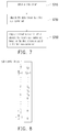
- FIG. 7 is flowchart illustrating a method of data allocation according to an embodiment of the invention.
- the method of this embodiment is suitable for the wireless transmitting apparatuses 210 and 410.
- the control method of the embodiment of the invention is described with reference to the respective components of the wireless transmitting apparatuses 210 and 410. Steps in the method may be correspondingly modified based on the actual situation, and are not limited to the following.
- the processing circuit 216 obtains a data stream. Specifically, the processing circuit 216 converts a bit string from serial into parallel. Then, based on the number of sub-carriers (or Fourier computation points, such as 128, 256, or 1024, etc,) and adopted coding/modulation, the bit string is modulated (through phase-shift keying (PSK) differential phase-shift keying (DPSK), quadrature amplitude modulation (QAM), and quadrature phase-shift keying (QPSK), etc., for example) into a complex data stream. For example, a bit string 111001 is modulated into 1+j, 1-j, -1+j after modulation if QPSK modulation is used.
- PSK phase-shift keying
- DPSK differential phase-shift keying
- QAM quadrature amplitude modulation
- QPSK quadrature phase-shift keying
- part or all the data in the data steam may also be specific pilot signals.
- the invention does not intend to limit the way that the data stream is generated.
- the processing circuit 216 allocates the data stream to a first sub-carrier set. All the sub-carriers are divided into the first sub-carrier set and a second sub-carrier set, and the first and second sub-carrier sets respectively have sub-carriers with opposite frequencies to each other.
- s k is data allocated to a sub-carrier index k (i.e., a modulation signal carried by a k th sub-carrier)
- f d is a sub-carrier spacing
- 1/ f d is a symbol period
- t is a time variable.
- the first sub-carrier set includes the first sub-carrier to the (N/2)-1 th sub-carrier
- the second sub-carrier set includes the -(N/2)+1 th sub-carrier to the -1 st sub-carrier.
- the first sub-carrier set includes positive sub-carrier indices
- the second sub-carrier set includes negative sub-carrier indices.
- the processing circuit 216 allocates data in the data stream in the subset of the first sub-carrier to the N/2 th sub-carrier in the first sub-carrier set.
- -1+j is allocated to the first sub-carrier of the first sub-carrier set and 1-j is allocated to the second sub-carrier of the first sub-carrier set.
- -1+j is allocated to the second sub-carrier of the first sub-carrier set, and 1-j is allocated to the first sub-carrier of the first sub-carrier set.
- the processing circuit 216 empties the second sub-carrier set allocates the second sub-carrier set based on the data stream allocated to the first sub-carrier set. Specifically, to prevent the receiving module 253 having a single branch receiver from being influenced by the inter-carrier interference, derivation is made in the embodiment of the invention based on the formulae of the received signals representing the data stream flowing through the components and the modules of the wireless transmitting apparatus 210 and the wireless receiving apparatus 250, so as to draw the conclusion that the data signal carried by the sub-carrier -n may interfere the data signal carried by the sub-carrier n. Therefore, allocating data carried by the sub-carriers in the second sub-carrier set would be according to the conclusion.
- the OFDM symbol output by the processing circuit 216 to the transmitting module 213 may be represented as Formula (1).
- Formula (3) is obtained after performing complex conjugate computation to the OFDM symbols (as represented in Formula (1)) output to the transmitting module 213.
- the radio frequency signal after being received by the antenna unit 652 may be represented in Formula (4).
- ⁇ 1
- the wireless channel is described as a single tap impulse response also for the ease of description.
- the embodiments of the invention are extensively applicable to circumstances with a multi-tap impulse response (i.e., multi-path channel) and a long delay time (e.g., tens of sample durations). Namely, ⁇ may be greater than a single sampling assumed in most OFDM-based systems.
- an output signal r L ( t ) of the signal r I ( t ) processed by the filter 653_7 may be represented as Formula (6).
- Formulae (1) and (7) By combining Formulae (1) and (7) with Formula (6), a linear combination of a sub-carrier e j 2 ⁇ k f d t k ⁇ - N 2 + 1 , ... , N 2 may be obtained.
- Formula (8) may also be represented by the linear combination of the sub-carrier e j 2 ⁇ k f d t k ⁇ - N 2 + 1 , ... , N 2 , a signal that Formula (8) represents may also be an OFDM signal.
- the processing circuit 256 or 656 proceeds to sample and perform the Fourier transformation (e.g., fast Fourier transformation, discrete Fourier transformation, etc.,) to the signal r L ( t )
- the received signal is not interfered by a negative frequency, and the processing circuit 256 may further proceed to demodulate or decode, so as to restore the data stream.
- the processing circuit 216 performs complex conjugate computation to the data stream allocated to the first sub-carrier set, and the data stream after the complex conjugate computation is allocated to the second sub-carrier set. In this embodiment, the processing circuit 216 allocates data of an m th sub-carrier that after the conjugate computation to an -mth sub-carrier in the second sub-carrier set.
- m is from 1 to (N/2)-1.
- the received signal is not interfered by a negative frequency, either, and the processing circuit 256 may further proceed to demodulate and decode, so as to restore the data stream.
- the processing circuit 216 After allocating all the sub-carriers based on the method of data allocation, the processing circuit 216 converts the allocated data stream into the OFDM signal. Specifically, the processing circuit may perform N-point (i.e., the total number of the sub-carriers) inverse Fourier transformation (e.g., FFT, DFT, etc.,), so as to add up the data carried by the sub-carriers, thereby forming the OFDM symbol. Then, as time changes, several consecutive OFDM symbols form an OFDM signal, and the OFDM signal is output to the transmitting module 213 through the processing circuit 216. Finally, the transmitting module 213 transmits the OFDM signal to the external environment (e.g., transmitting to the wireless receiving apparatus 250) through the antenna unit 212.
- N-point i.e., the total number of the sub-carriers
- inverse Fourier transformation e.g., FFT, DFT, etc.
- FIG. 10 is flowchart illustrating a method of signal receiving according to an embodiment of the invention.
- the method of this embodiment is suitable for the wireless receiving apparatuses 250 and 650.
- the control method of the embodiment of the invention is described with reference to the respective components of the wireless transmitting apparatuses 250 and 650. Steps in the method may be correspondingly modified based on the actual situation, and are not limited to the following.
- the receiving module 253 receives a radio frequency signal through a single branch receiver and generates a baseband signal. All the sub-carriers are divided into the first sub-carrier set and the second sub-carrier set, and the radio frequency signal includes the OFDM signal carried by the first sub-carrier set and the second sub-carrier set, and the second sub-carrier set is emptied or allocated based on data of the first sub-carrier set.
- the processing circuit 256 restores the data stream from the baseband signal. Details concerning Steps S1010 and S1030 may be referred to Steps S730 to S750 in FIG. 7 , and thus will not be reiterated hereinafter.
- the processing circuit 256 may further restore the data of the original data stream s k from the received signal r k based on the chosen method of data collocation. For example, the processing circuit 256 may obtain a phase shift ⁇ based on a channel estimation technology, so as to effectively restore the data stream.
- the received signal r k may be with amplitude attenuation.
- People using the embodiments of the invention may further multiply an amplitude of the data stream with a multiple (e.g., 4, 4/N, etc.,) by using the processing circuit 216, amplify based on a gain (e.g., 4, 4/N, etc.,) by using an amplifying circuit in the transmitting module 213, amplify based on a gain by using an amplifying circuit 653_1 of the transmitting module 213, multiply the received signal r k with a multiple by using the processing circuit 216, etc.
- the invention is not limited thereto.
- Steps S730 to S750 in FIG. 7 are described with the in-phase path only.
- the method of data allocation according to the embodiments of the invention is also applicable for receiving only with the quadrature-phase path.
- the wireless receiving apparatus only includes the single branch receiver, so as to prevent the in-phase/quadrature-phase imbalance in the conventional dual branch receiver and simplify the hardware structure.
- the wireless receiving apparatus is applicable in low-cost wireless communication apparatus used in the Internet of Things (IoT) (which may include machine type communication (MTC) and device-to-device (D2D) communication).
- IoT Internet of Things
- MTC machine type communication
- D2D device-to-device
- the wireless transmitting apparatus is used in the embodiments of the invention to set a portion of the sub-carriers as null sub-carriers or as conjugate values of the other portion of the sub-carriers. Accordingly, the wireless receiving apparatus according to the embodiments of the invention may operate effectively without inter-carrier interference.
Landscapes
- Engineering & Computer Science (AREA)
- Signal Processing (AREA)
- Computer Networks & Wireless Communication (AREA)
- Physics & Mathematics (AREA)
- Discrete Mathematics (AREA)
- General Physics & Mathematics (AREA)
- Mathematical Physics (AREA)
- Mobile Radio Communication Systems (AREA)
Abstract
Description
- The invention relates an orthogonal frequency division multiplexing (OFDM) technology, and particularly relates to a method of data allocation, a wireless transmitting apparatus using the same, a signal receiving method and a wireless receiving apparatus using the same based on the OFDM technology.
- Owing to advantages such as having a better efficiency of the frequency spectrum, effectively coping with multipath channel, and having a high data transmission speed, the orthogonal frequency division modulation technology has been broadly used in relevant fields of communication such as digital television broadcasting, accessing the Internet of digital subscriber lines (DSL), and 4G mobile communication networks, etc.
-
FIG. 1 shows a conventional dual branch orthogonal frequency division multiplexing receiving device. Referring toFIG. 1 , it is assumed that areceiving device 100 has two antenna units 111 andcorresponding receivers corresponding receiver 110. After being received by using theantenna unit 110, a radio frequency signal (Z1(t)) is divided into two paths, i.e., an in-phase path (I-path) 150 and a quadrature-phase path (Q-path) 155. - In the in-
phase path 150, thefrequency mixer 112 performs a mixing process (i.e., multiplying I LO1 (t) = cos(2πfct) by using a multiplier) based on a carrier frequency fc generated by anoscillation generator 113, and the signal is processed by a low pass filter (LPF) 116 and an analog-to-digital converter 118, so as to generate a baseband signal (IBB1(t)) of the in-phase path 150. Besides, in the quadrature-phase path 155, amixer 114 performs a mixing process based on the carrier frequency fc generated by theoscillation generator 113 and rotates the phase 90°+θ1, then the signal is processed by anamplifier 115 with a gain g1 (i.e., multiplying Q LO1 (t) = -g 1 sin(2πf c t + θ1) by using a multiplier) and processed by alow pass filter 117 and a analog-to-digital converter 119, so as to generate a baseband signal (QBB1(t)) of the quadrature-path 155. Then, the baseband signals (IBB1(t) and QBB(t)) are transmitted to a signal processing module 170 (e.g., a long term evolution (LTE) modem). - However, since the in-phase path and the quadrature-phase path are both present, the dual branch orthogonal frequency division multiplexing receiver usually faces an in-phase/quadrature-phase imbalance.
- The invention provides a method of data allocation, a method of signal receiving, a wireless transmitting apparatus, and a wireless receiving apparatus. In the methods and apparatuses, data of sub-carriers are allocated by the wireless transmitting apparatus, and the wireless receiving apparatus has a single branch receiver to receive signals, so as to effectively solve an in-phase/quadrature-phase imbalance and provide a structure of a low-cost receiving apparatus.
- A method of data allocation according to an embodiment of the invention is suitable for a wireless transmitting apparatus. The wireless transmitting apparatus transmits through a plurality of sub-carriers based on an orthogonal frequency division multiplexing (OFDM) technology. The method of data allocation includes steps as follows. A data stream is obtained. The data stream is allocated to a first sub-carrier set. All the sub-carriers are divided into the first sub-carrier set and a second sub-carrier set, and the first and second sub-carrier sets respectively have the sub-carriers with opposite frequencies to each other. Then, the second sub-carrier set is emptied or allocated based on the data stream allocated to the first sub-carrier set.
- A wireless transmitting apparatus according to an embodiment of the invention is suitable for transmitting through a plurality of sub-carriers based on an orthogonal frequency division multiplexing technology. The wireless transmitting apparatus includes a transmitting module and a processing circuit. The transmitting module transmits an OFDM signal. The processing circuit is coupled to the transmitting module and configured to perform steps as follows. A data stream is obtained. The data stream is allocated to a first sub-carrier set. All the sub-carriers are divided into the first sub-carrier set and a second sub-carrier set, and the first and second sub-carrier sets respectively have the sub-carriers with opposite frequencies to each other. The second sub-carrier set is emptied or allocated based on the data stream allocated to the first sub-carrier set. Then, the data stream allocated to the first sub-carrier set and the second sub-carrier set are converted into an OFDM signal, so as to transmit the OFDM signal through the transmitting module.
- A wireless receiving apparatus according to an embodiment of the invention is suitable for receiving through a plurality of sub-carriers based on an OFDM technology. The wireless receiving apparatus includes a receiving module and a processing circuit. The receiving module includes a single branch receiver that receives a radio frequency signal and outputs a baseband signal. All the sub-carriers are divided into the first sub-carrier set and the second sub-carrier set, and the radio frequency signal includes the OFDM signal carried by the first sub-carrier set and the second sub-carrier set, and the second sub-carrier set is emptied or allocated based on data of the first sub-carrier set. The processing circuit is coupled to the receiving module and configured to perform steps as follows. A data stream is restored from the baseband signal.
- A method of signal receiving according to an embodiment of the invention is suitable for a wireless receiving apparatus. The wireless receiving apparatus receives through a plurality of sub-carriers based on an OFDM technology. The method of signal receiving includes steps as follows. A radio frequency signal is received through a single branch receiver and a baseband signal is generated. All the sub-carriers are divided into the first sub-carrier set and the second sub-carrier set, and the radio frequency signal includes the OFDM signal carried by the first sub-carrier set and the second sub-carrier set, and the second sub-carrier set is emptied or allocated based on data of the first sub-carrier set. Then, a data stream is restored from the baseband signal.
- Based on above, in the method of data allocation and the wireless transmitting apparatus using the same and the method of signal receiving and the wireless receiving apparatus using the same according to the embodiments of the invention, the wireless transmitting apparatus empties a portion of the sub-carriers or allocates the portion of the sub-carriers based on the data of the other portion of the sub-carriers, so that the wireless receiving apparatus that receives by using the single branch receiver is able to effectively restore the data stream and prevent the in-phase/quadrature-phase imbalance and inter-carrier interference (ICI).
- In order to make the aforementioned and other features and advantages of the invention comprehensible, several exemplary embodiments accompanied with figures are described in detail below.
- The accompanying drawings are included to provide a further understanding of the invention, and are incorporated in and constitute a part of this specification. The drawings illustrate embodiments of the invention and, together with the description, serve to explain the principles of the invention.
-
FIG. 1 shows a conventional dual branch orthogonal frequency division multiplexing receiver. -
FIG. 2 is a schematic diagram illustrating a communication system according to an embodiment of the invention. -
FIG. 3 is a block diagram illustrating a wireless transmitting apparatus according to an embodiment of the invention. -
FIG. 4 is a schematic diagram illustrating a circuit of a wireless transmitting apparatus according to an embodiment of the invention. -
FIG. 5 is a block diagram illustrating a wireless receiving apparatus according to an embodiment of the invention. -
FIG. 6 is a schematic diagram illustrating a circuit of a wireless transmitting apparatus according to an embodiment of the invention. -
FIG. 7 is flowchart illustrating a method of data allocation according to an embodiment of the invention. -
FIG. 8 is a schematic diagram illustrating data allocation. -
FIG. 9 is a schematic diagram illustrating data allocation. -
FIG. 10 is flowchart illustrating a method of signal receiving according to an embodiment of the invention. - Reference will now be made in detail to the present preferred embodiments of the invention, examples of which are illustrated in the accompanying drawings. Wherever possible, the same reference numbers are used in the drawings and the description to refer to the same or like parts.
- Compared with the conventional dual branch receiver, a single branch receiver has a lower cost and is capable of preventing in-phase/quadrature-path imbalance. However, when a dual path design (i.e., in-phase path and quadrature-phase path) is not used, there may be an inter-carrier interference (ICI) after a base signal undergoes a discrete Fourier transformation (DFT) of an orthogonal frequency division multiplexing (OFDM) receiving apparatus. The inter-carrier interference usually occurs between a positive sub-carrier index and a corresponding negative sub-carrier index. Taking a data signal carried by a sub-carrier n as an example, an interference to the data signal may result from a data signal carried by a sub-carrier -n. Accordingly, in the embodiments of the invention, a data allocation or a specific coding may be performed on a wireless transmitting apparatus, so as to eliminate the inter-carrier interference formed when the single branch receiver is used to receive an OFDM signal. In the following, a plurality of embodiments following the spirit of the invention are described in detail. People using these embodiments may suitably modify these embodiments based on the needs, and the invention is not limited to the descriptions in the following.
-
FIG. 2 is a schematic diagram illustrating a communication system according to an embodiment of the invention. Referring toFIG.2 , acommunication system 200 includes awireless transmitting apparatus 210 and awireless receiving apparatus 250. Thecommunication system 200 is compatible with a communication system based on the OFDM technology, such as a 4G mobile communication network, a wireless local access network (WLAN), or a digital television broadcast system. It should be noted that thecommunication system 200 may include one or more of thewireless transmitting apparatuses 210 and thewireless receiving apparatuses 250, and the invention is not limited by the numbers thereof. - The
wireless transmitting apparatus 210 may be implemented by a variety of embodiments. For example, thewireless transmitting apparatus 210 may include, but is not limited to, a mobile station, an advanced mobile station (AMS), a user equipment (UE), a server, a client terminal, a desktop computer, a laptop computer, a network computer, a work station, a personal digital assistant (PDA), a tablet personal computer (PC), a scanner, a telecommunication apparatus, a pager, a camera, an access point, a television, a pocket video gaming apparatus, a music apparatus, a wireless sensor, etc. -
FIG. 3 is a block diagram illustrating thewireless transmitting apparatus 210 according to an embodiment of the invention. Thewireless transmitting apparatus 210 may at least be represented by functional components shown inFIG. 3 . Thewireless transmitting apparatus 210 may at least include, but is not limited to, a transmittingmodule 213, aprocessing circuit 216, astorage module 215, and one ormore antenna units 212. The transmittingmodule 213 transmits downlink signals wirelessly. The transmittingmodule 213 may also perform operations such as low-pass amplification, impedance matching, frequency mixing, up conversion, filtering, amplification, digital-to-analog conversion, and other similar operations. The transmittingmodule 213 may be integrated into a chip or implemented as an independent component or module, and the transmitting module may be implemented as hardware or software. - The
storage module 215 may be a static or mobile random access memory (RAM), read-only memory (ROM), flash memory, hard drive, other similar apparatuses, or a combination of the aforesaid apparatuses. - The
processing circuit 216 is configured to process digital signals and perform a method of data allocation according to an exemplary embodiment of the invention. In addition, theprocessing circuit 216 is coupled to thestorage module 215 to store programming codes, configuration of apparatus, codebook, buffer or permanent data. In addition, thestorage module 215 may also record a plurality of modules executed by theprocessing circuit 216. For example, theprocessing circuit 216 may load a digital signal processing module for signal processing such as generating data streams, coding, serial-to-parallel conversion and/or parallel-to-serial conversion, constellation mapping, modulating, adding pilot signals and/or guard interval, inverse Fourier transformation (e.g., fast Fourier transformation (FFT), discrete Fourier transformation (DFT)), etc. Alternatively, theprocessing circuit 216 may load a communication signaling processing module, so as to control signaling messages based on related communication technologies (e.g., WiFi, LTE, etc.). - The function of the
processing circuit 216 may be implemented by using a programmable unit such as a micro-processor, a micro-controller, a digital signal processing (DSP) chip, a field programmable gate array (FPGA), etc. The function of theprocessing circuit 216 may also be implemented by using an independent electronic apparatus or an integrated circuit (IC). Besides, theprocessing circuit 216 may be implemented as hardware or software. It should be noted that, based on the design needs of people using the embodiments of the invention, thewireless transmitting apparatus 210 may have one ormore processing circuits 216 to integrate or separately deal with the function of a modem and functions of sensing and displaying, etc. The invention does not intend to impose limitations in this regard. -
FIG. 4 is a schematic diagram illustrating a circuit of a wireless transmitting apparatus according to an embodiment of the invention. Referring toFIG. 4 , awireless transmitting apparatus 410 includes anantenna unit 412, a transmittingmodule 413, and aprocessing circuit 416. Theprocessing circuit 416 respectively outputs a real part and an imaginary part of a data stream to thetransmitting module 413. The transmittingmodule 413 includes digital-to-analog converters 413_1 and 413_2, frequency mixers 413_3 and 413_5, an oscillation generator 413_4, a phase rotator 413_6 and a multiplexer 413_7. The real part and the imaginary part of the data stream are respectively converted by the digital-to-analog converters 413_1 and 413_2, and are up converted by the frequency mixer 413_3 and 413_5 based on a carrier frequency generated by the oscillation generator 413_4. In addition, the phase of the imaginary part is further rotated 90°+θ2 by the phase rotator 413_6. Then, the real part and the imaginary part of the data stream are emitted to an external environment after being multiplexed by the multiplexer 413_7. - It should be noted that the
wireless transmitting apparatus 410 may also have a plurality of theantenna units 412 and corresponding transmittingmodules 413. The invention does not intend to limit the numbers of theantenna unit 412 and thetransmitting module 413. - Besides, the
wireless receiving apparatus 250 may be implemented by a plurality of embodiments. For example, thewireless receiving apparatus 250 may include, but is not limited to, a mobile station, an advanced mobile station, a server, a client terminal, a desktop computer, a laptop computer, a UE, a network computer, a work station, a personal digital assistant, a tablet personal computer, a scanner, a telecommunication apparatus, a pager, a camera, an access point, a television, a pocket video gaming apparatus, a music apparatus, a wireless sensor, etc. -
FIG. 5 is a block diagram illustrating thewireless receiving apparatus 250 according to an embodiment of the invention. Thewireless receiving apparatus 250 may at least be represented by functional components shown inFIG. 5 . Thewireless receiving apparatus 250 may at least include, but is not limited to, a receivingmodule 253, aprocessing circuit 256, astorage module 255, and one ormore antenna units 252. The receivingmodule 253 includes a single branch receiver (e.g., only including an in-phase path or a quadrature-phase path). The receivingmodule 253 may also perform operations such as low-pass amplification, impedance matching, frequency mixing, down conversion, filtering, amplification, analog-to-digital conversion, and other similar operations. The receivingmodule 253 may be integrated into a chip or implemented as an independent component or module, and thetransmitting module 253 may be implemented as hardware or software. - The
storage module 255 may be a static or mobile random access memory (RAM), read-only memory (ROM), flash memory, hard drive, other similar apparatuses, or a combination of the aforesaid apparatuses. - The
processing circuit 256 is configured to process digital signals and perform a method of data allocation according to an exemplary embodiment of the invention. In addition, theprocessing circuit 256 is coupled to thestorage module 255 to store programming codes, configuration of apparatus, codebook, buffer or permanent data. In addition, thestorage module 215 may also record a plurality of modules executed by theprocessing circuit 256. For example, theprocessing circuit 256 may load a digital signal processing module for signal processing such as generating data streams, coding, serial-to-parallel and/or parallel-to-serial conversion, constellation mapping, demodulating, channel estimation, equalization, synchronization, Fourier transformation, symbol detecting, etc. Alternatively, theprocessing circuit 256 may load a communication signaling processing module, so as to control signaling messages based on related communication technologies. - The function of the
processing circuit 256 may be implemented by using a programmable unit such as a micro-processor, a micro-controller, a digital signal processing chip, a field programmable gate array, etc. The function of theprocessing circuit 256 may also be implemented by using an independent electronic apparatus or an integrated circuit (IC). Besides, theprocessing circuit 256 may also be implemented as hardware or software. It should be noted that, based on the design needs of people using the embodiments of the invention, thewireless receiving apparatus 250 may have one ormore processing circuits 256 to integrate or separately deal with the function of a modem and functions of sensing and displaying, etc. The invention does not intend to impose limitations in this regard. -
FIG. 6 is a schematic diagram illustrating a circuit of a wireless transmitting apparatus according to an embodiment of the invention. Referring toFIG. 6 , awireless receiving apparatus 650 includes anantenna unit 652, a transmittingmodule 653, and aprocessing circuit 656. The receivingmodule 653 includes a single branch receiver having an amplifying circuit 653_1, a frequency mixer 653_3, an oscillation generator 653_5, a filter 653_7, and an analog-to-digital converter 653_9. The amplifying circuit 653_1 receives a radio frequency signal (r(t)). The frequency mixer 653_3 down converts the radio frequency signal based on a carrier frequency generated by the oscillation generator 653_5 (i.e., multiplying cos(2πfct) by using a multiplier). The filter 653_7 filters (by performing low-pass filtering, band-pass filtering, or filtering at a specific frequency or at a specific frequency band, for example) the down converted radio frequency signal. Moreover, the analog-to-digital converter 653_9 converts the filtered radio frequency signal into a baseband signal IBB(t). Then, the receivingmodule 653 outputs the baseband signal to theprocessing circuit 656. - Referring to
FIGs. 1 and6 , it should be noted that, as compared with the dual branch OFDM receiver inFIG. 1 , the receivingmodule 653 only uses the in-phase path without using the quadrature-phase path. In this way, the hardware cost is reduced. In some other embodiments, it is also plausible that the receivingmodule 253 only uses the quadrature-phase path (e.g., the quadrature-phase path 155 ofFIG. 1 ) without using the in-phase path. Besides thewireless receiving module 650 may also have a plurality of theantenna units 652 and the corresponding receivingmodules 653. The invention does not intend to limit the numbers of theantenna units 652 and the transmittingmodules 653. - To better describe the operational flow of the embodiments of the invention, several embodiments are described in detail in the following to set forth a method of data allocation and a method of signal receiving according to the embodiments of the invention.
FIG. 7 is flowchart illustrating a method of data allocation according to an embodiment of the invention. Referring toFIG. 7 , the method of this embodiment is suitable for thewireless transmitting apparatuses wireless transmitting apparatuses - At Step 710, the
processing circuit 216 obtains a data stream. Specifically, theprocessing circuit 216 converts a bit string from serial into parallel. Then, based on the number of sub-carriers (or Fourier computation points, such as 128, 256, or 1024, etc,) and adopted coding/modulation, the bit string is modulated (through phase-shift keying (PSK) differential phase-shift keying (DPSK), quadrature amplitude modulation (QAM), and quadrature phase-shift keying (QPSK), etc., for example) into a complex data stream. For example, a bit string 111001 is modulated into 1+j, 1-j, -1+j after modulation if QPSK modulation is used. - It should be noted that, based on different design needs, part or all the data in the data steam may also be specific pilot signals. The invention does not intend to limit the way that the data stream is generated.
- At Step S730, the
processing circuit 216 allocates the data stream to a first sub-carrier set. All the sub-carriers are divided into the first sub-carrier set and a second sub-carrier set, and the first and second sub-carrier sets respectively have sub-carriers with opposite frequencies to each other. Specifically, it is assumed that an OFDM symbol in the N point (e.g., 64, 512, or 1024, etc.,) fast Fourier transformation may be represented in the time domain as Formula (1):
- In this embodiment, based on Formula (1), the first sub-carrier set includes the first sub-carrier to the (N/2)-1th sub-carrier, and the second sub-carrier set includes the -(N/2)+1th sub-carrier to the -1st sub-carrier. Namely, the first sub-carrier set includes positive sub-carrier indices, and the second sub-carrier set includes negative sub-carrier indices. The
processing circuit 216 allocates data in the data stream in the subset of the first sub-carrier to the N/2th sub-carrier in the first sub-carrier set. For example, assuming that N is 8 and the data stream includes -1+j, 1-j, 1+j..., then -1+j is allocated to the first sub-carrier of the first sub-carrier set and 1-j is allocated to the second sub-carrier of the first sub-carrier set. Alternatively, -1+j is allocated to the second sub-carrier of the first sub-carrier set, and 1-j is allocated to the first sub-carrier of the first sub-carrier set. - At Step S750, the
processing circuit 216 empties the second sub-carrier set allocates the second sub-carrier set based on the data stream allocated to the first sub-carrier set. Specifically, to prevent thereceiving module 253 having a single branch receiver from being influenced by the inter-carrier interference, derivation is made in the embodiment of the invention based on the formulae of the received signals representing the data stream flowing through the components and the modules of thewireless transmitting apparatus 210 and thewireless receiving apparatus 250, so as to draw the conclusion that the data signal carried by the sub-carrier -n may interfere the data signal carried by the sub-carrier n. Therefore, allocating data carried by the sub-carriers in the second sub-carrier set would be according to the conclusion. - In the following, details concerning the
wireless transmitting apparatus 210 are described. Based on Step S750, the OFDM symbol output by theprocessing circuit 216 to thetransmitting module 213 may be represented as Formula (1). Then, referring toFIG. 4 , after the up conversion by the frequency mixers 413_3 and 413_5 and the multiplexing by the multiplexer 413_7, the OFDM symbol output by theantenna unit 412 may be represented as Formula (2):
transmitting module 213.
- Then, details concerning the
wireless receiving apparatus 250 are described in the following. If a wireless channel that an OFDM signal emitted by thewireless transmitting apparatus 210 passes has a single tap impulse response h(t) = αδ(t-π), where α is an attenuation parameter at an arbitrary positive value, while τ is a delay time parameter at an positive value. Referring toFIG. 6 , the radio frequency signal after being received by theantenna unit 652 may be represented in Formula (4).
- It should be noted that, to make the description simpler, the value of τ is assumed to be very small to make d(t) ≈ d(t -τ), and it is assumed that α = 1. However, the invention is not limited thereto. Besides, the wireless channel is described as a single tap impulse response also for the ease of description. The embodiments of the invention are extensively applicable to circumstances with a multi-tap impulse response (i.e., multi-path channel) and a long delay time (e.g., tens of sample durations). Namely, τ may be greater than a single sampling assumed in most OFDM-based systems.
- An output signal rI (t) after the radio frequency signal is processed by the frequency mixer of the in-phase path may be represented as Formula (5):

- Then, an output signal rL (t) of the signal rI (t) processed by the filter 653_7 may be represented as Formula (6).


- By combining Formulae (1) and (7) with Formula (6), a linear combination of a
sub-carrier 

- Since Formula (8) may also be represented by the linear combination of the
sub-carrier 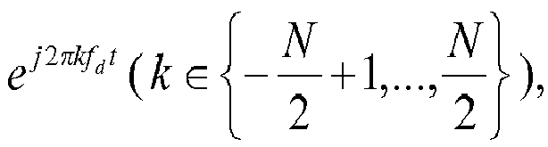
processing circuit 
- Based on Formula (9), it can be known that if the receiving
module 253 only has the in-phase path (without having the quadrature-phase path), receiving a signal in a frequency domain of the sub-carrier k may be interfered by the sub-carrier -k. Thus, to make the OFDM-basedwireless receiving apparatus 250 having only the in-phase path operable, a method of data allocation according to an embodiment of the invention is provided in the following. - In an embodiment, the
processing circuit 216 sets the sub-carriers in the second sub-carrier set as null sub-carrier. Specifically, in a designated single OFDM symbol, it is assumed that theprocessing circuit 216 allocates a modulation signal sk to the kth sub-carrier (included in the first sub-carrier set) of the positive sub-carrier index (as in Step S730), and the -kth sub-carrier (included in the second sub-carrier set) of the negative sub-carrier index is set as a null sub-carrier. In other words, s-k = 0, the data carried by the -kth sub-carrier in the second sub-carrier set are all null. Referring to a schematic diagram illustrating data allocation as shown inFIG. 8 , data of the sub-carrier indices n, where n ranges from n = -1 to n = -(N/2)+1, are all null values. Thus, at thewireless receiving apparatus 250, the received signal of the kth sub-carrier may be represented as Formula (10):
processing circuit 256 may further proceed to demodulate or decode, so as to restore the data stream. - In another embodiment, the
processing circuit 216 performs complex conjugate computation to the data stream allocated to the first sub-carrier set, and the data stream after the complex conjugate computation is allocated to the second sub-carrier set. In this embodiment, theprocessing circuit 216 allocates data of an mth sub-carrier that after the conjugate computation to an -mth sub-carrier in the second sub-carrier set. Here, m is from 1 to (N/2)-1. Specifically, in the designated single orthogonal frequency division symbol, it is assumed that theprocessing circuit 216 allocates a modulation signal sm to the mth sub-carrier (included in the first sub-carrier set) of the positive sub-carrier index (as Step S730), and the -mth sub-carrier (included in the second sub-carrier set) of the negative sub-carrier index is set as a conjugate value of the modulation signal carried by the mth sub-carrier, namely
FIG. 9 , data of the sub-carrier indices n, where n ranges from n = -1 to n = -(N/2)+1, are respectively conjugate values of data carried by the sub-carrier indices, where n from n = 1 to n = (N/2)-1. Thus, at thewireless receiving apparatus 250, the received signal of the kth sub-carrier may be represented as Formula (11):
processing circuit 256 may further proceed to demodulate and decode, so as to restore the data stream. - After allocating all the sub-carriers based on the method of data allocation, the
processing circuit 216 converts the allocated data stream into the OFDM signal. Specifically, the processing circuit may perform N-point (i.e., the total number of the sub-carriers) inverse Fourier transformation (e.g., FFT, DFT, etc.,), so as to add up the data carried by the sub-carriers, thereby forming the OFDM symbol. Then, as time changes, several consecutive OFDM symbols form an OFDM signal, and the OFDM signal is output to thetransmitting module 213 through theprocessing circuit 216. Finally, the transmittingmodule 213 transmits the OFDM signal to the external environment (e.g., transmitting to the wireless receiving apparatus 250) through theantenna unit 212. - In another perspective,
FIG. 10 is flowchart illustrating a method of signal receiving according to an embodiment of the invention. Referring toFIG. 10 , the method of this embodiment is suitable for thewireless receiving apparatuses wireless transmitting apparatuses - At Step S1010, the receiving
module 253 receives a radio frequency signal through a single branch receiver and generates a baseband signal. All the sub-carriers are divided into the first sub-carrier set and the second sub-carrier set, and the radio frequency signal includes the OFDM signal carried by the first sub-carrier set and the second sub-carrier set, and the second sub-carrier set is emptied or allocated based on data of the first sub-carrier set. At Step S1030, theprocessing circuit 256 restores the data stream from the baseband signal. Details concerning Steps S1010 and S1030 may be referred to Steps S730 to S750 inFIG. 7 , and thus will not be reiterated hereinafter. In other words, if the receivingmodule 253 receives the OFDM signal generated based on the method of data allocation, the inter-carrier interference does not occur. Besides, theprocessing circuit 256 may further restore the data of the original data stream sk from the received signal rk based on the chosen method of data collocation. For example, theprocessing circuit 256 may obtain a phase shift θ based on a channel estimation technology, so as to effectively restore the data stream. - It should be noted that, based on Formulae (10) and (11), it can be known that the received signal rk may be with amplitude attenuation. People using the embodiments of the invention may further multiply an amplitude of the data stream with a multiple (e.g., 4, 4/N, etc.,) by using the
processing circuit 216, amplify based on a gain (e.g., 4, 4/N, etc.,) by using an amplifying circuit in thetransmitting module 213, amplify based on a gain by using an amplifying circuit 653_1 of the transmittingmodule 213, multiply the received signal rk with a multiple by using theprocessing circuit 216, etc. However, the invention is not limited thereto. In addition Steps S730 to S750 inFIG. 7 are described with the in-phase path only. However, in other embodiments, the method of data allocation according to the embodiments of the invention is also applicable for receiving only with the quadrature-phase path. - In view of the foregoing, the wireless receiving apparatus according to the embodiments of the invention only includes the single branch receiver, so as to prevent the in-phase/quadrature-phase imbalance in the conventional dual branch receiver and simplify the hardware structure. Thus, the wireless receiving apparatus according to the embodiment is applicable in low-cost wireless communication apparatus used in the Internet of Things (IoT) (which may include machine type communication (MTC) and device-to-device (D2D) communication). In addition, to avoid the inter-carrier interference in the wireless receiving apparatus having only the single branch receiver, the wireless transmitting apparatus is used in the embodiments of the invention to set a portion of the sub-carriers as null sub-carriers or as conjugate values of the other portion of the sub-carriers. Accordingly, the wireless receiving apparatus according to the embodiments of the invention may operate effectively without inter-carrier interference.
Claims (20)
- A method of data allocation, suitable for a wireless transmitting apparatus (210, 410), wherein the wireless transmitting apparatus (210, 410) transmits through a plurality of sub-carriers based on an orthogonal frequency division multiplexing, named OFDM hereinafter, technology, the method comprising:obtaining a data stream;allocating the data stream to a first sub-carrier set, wherein all the sub-carriers are divided into the first sub-carrier set and a second sub-carrier set, and the first sub-carrier set and the second sub-carrier set respectively have the sub-carriers with opposite frequencies to each other; andemptying the second sub-carrier set or allocating the second sub-carrier set based on the data stream allocated to the first sub-carrier set.
- The method of data allocation as claimed in claim 1, wherein the step of emptying the second sub-carrier set or allocating the second sub-carrier set based on the data stream allocated to the first sub-carrier set comprises:setting the sub-carriers in the second sub-carrier set as a plurality of null sub-carriers.
- The method of data allocation as claimed in claim 1 or 2, wherein the step of emptying the second sub-carrier set or allocating the second sub-carrier set based on the data stream allocated to the first sub-carrier set comprises:performing a complex conjugate computation to the data stream allocated to the first sub-carrier set; andallocating the data stream after the complex conjugate computation to the second sub-carrier set.
- The method of data allocation as claimed in any of the claims 1 to 3, wherein the number of the sub-carriers is N, the first sub-carrier set comprises a first sub-carrier to an (N/2)-1th sub-carrier, the second sub-carrier set comprises an -(N/2)+1th sub-carrier to a -1st sub-carrier, and the step of allocating the data stream after the complex conjugate computation to the second sub-carrier set comprises:allocating data stream after the complex conjugate computation in an mth sub-carrier in the first sub-carrier set to an -mth sub-carrier in the second sub-carrier set, wherein m is from 1 to (N/2)-1.
- The method of data allocation as claimed in any of the claims 1 to 4, wherein after the step of emptying the second sub-carrier set or allocating the second sub-carrier set based on the data stream allocated to the first sub-carrier set, the method further comprises:converting the allocated data stream into an OFDM signal.
- A wireless transmitting apparatus (210, 410), suitable to transmit through a plurality of sub-carriers based on an OFDM technology, the apparatus comprising:a transmitting module (213, 413), transmitting an OFDM signal;a processing circuit (216, 416), coupled to the transmitting module (213, 413) and configured to perform the following:obtaining a data stream;allocating the data stream to a first sub-carrier set, wherein all the sub-carriers are divided into the first sub-carrier set and a second sub-carrier set, and the first sub-carrier set and the second sub-carrier set respectively have the sub-carriers with opposite frequencies to each other;emptying the second sub-carrier set or allocating the second sub-carrier set based on the data stream allocated to the first sub-carrier set; andconverting the data stream allocated to the first sub-carrier set and the second sub-carrier set into the OFDM signal, so as to transmit the OFDM signal through the transmitting module (213, 413).
- The wireless transmitting apparatus (210, 410) as claimed in claim 6, wherein the processing circuit (216, 416) is further configured to perform the following:setting the sub-carriers in the second sub-carrier set as a plurality of null sub-carriers.
- The wireless transmitting apparatus (210, 410) as claimed in claim 6 or 7, wherein the processing circuit (216, 416) is further configured to perform the following:performing a complex conjugate computation to the data stream allocated to the first sub-carrier set; andallocating the data stream after the complex conjugate computation to the second sub-carrier set.
- The wireless transmitting apparatus (210, 410) as claimed in any of the claims 6 to 8, wherein the number of the sub-carriers is N, the first sub-carrier set comprises a first sub-carrier to an (N/2)-1th sub-carrier, the second sub-carrier set comprises an -(N/2)+1th sub-carrier to a -1st sub-carrier, and the processing circuit (216, 416) is further configured to perform the following:allocating the data stream after the complex conjugate computation in an mth sub-carrier in the first sub-carrier set to an -mth sub-carrier in the second sub-carrier set, wherein m is from 1 to (N/2)-1.
- The wireless transmitting apparatus (210, 410) as claimed in any of the claims 8 to 9, wherein the processing circuit (216, 416) is further configured to perform the following:converting the allocated data stream into the OFDM signal.
- A wireless receiving apparatus (250, 650), suitable to receive through a plurality of sub-carriers based on an OFDM technology, the apparatus comprising:a receiving module (253, 653), comprising a single branch receiver that receives a radio frequency signal and outputs a baseband signal, wherein all the sub-carriers are divided into a first sub-carrier set and a second sub-carrier set, the radio frequency signal comprises an OFDM signal carried by the first sub-carrier set and the second sub-carrier set, and the second sub-carrier set is emptied or allocated based on data of the first sub-carrier set; anda processing circuit (256, 656), coupled to the receiving module (253, 653) and configured to perform the following:restoring a data stream from the baseband signal.
- The wireless receiving apparatus (250, 650) as claimed in claim 11, wherein the single branch receiver is only used for one of an in-phase path and a quadrature-phase path, and the single branch receiver comprises:an amplifying circuit (653_1), receiving the radio frequency signal through an antenna unit (252, 652);an oscillation generator (653_5), generating a carrier frequency;a frequency mixer (653_3), coupled to the amplifying circuit (653_) and the oscillation generator (653_5), and configured to perform down conversion to the radio frequency signal based on the carrier frequency;a filter (653_7), filtering the down converted radio frequency signal; andan analog-to-digital converter (653_9), coupled to the filter and configured to convert the filtered radio frequency signal into the baseband signal.
- The wireless receiving apparatus (250, 650) as claimed in claim 11 or 12, wherein in the OFDM signal, each of the sub-carriers in the second sub-carrier set carries a null value.
- The wireless receiving apparatus (250, 650) as claimed in any of the claims 11 to 13, wherein in the OFDM signal, data carried by the sub-carriers in the second sub-carrier set are conjugate with respect to data carried by the sub-carriers in the first sub-carrier set.
- The wireless receiving apparatus (250, 650) as claimed in any of the claims 11 to 14, wherein the number of the sub-carriers is N, the first sub-carrier set comprises a first sub-carrier to an (N/2)-1th sub-carrier, the second sub-carrier set comprises an -(N/2)+1th sub-carrier to a -1st sub-carrier, and data carried by an -mth sub-carrier in the second sub-carrier set are conjugate with respect to data carried by an mth sub-carrier in the first sub-carrier set, wherein m is from 1 to (N/2)-1.
- A method of signal receiving, suitable for a wireless receiving apparatus (250, 650), wherein the wireless receiving apparatus (250, 650) receives through a plurality of sub-carriers based on an OFDM technology, and the method comprises:receiving a radio frequency signal through a single branch receiver and generating a baseband signal, wherein all the sub-carriers are divided into a first sub-carrier set and a second sub-carrier set, the radio frequency signal comprises an orthogonal frequency division multiplexing signal carried by the first sub-carrier set and the second sub-carrier set, and the second sub-carrier set is emptied or allocated based on data of the first sub-carrier set; andrestoring a data stream from the baseband signal.
- The method of signal receiving as claimed in claim 16, wherein the single branch receiver is only used for one of an in-phase path and a quadrature-phase path.
- The method of signal receiving as claimed in any of the claims 16 or 17, wherein in the OFDM signal, each of the sub-carriers in the second sub-carrier set carries a null value.
- The method of signal receiving as claimed in any of the claims 16 to 18, wherein in the OFDM signal, data carried by the sub-carriers in the second sub-carrier set are conjugate with respect to data carried by the sub-carriers in the first sub-carrier set.
- The method of signal receiving as claimed in any of the claims 16 to 19, wherein the number of the sub-carriers is N, the first sub-carrier set comprises a first sub-carrier to an (N/2)-1th sub-carrier, the second sub-carrier set comprises an -(N/2)+1th sub-carrier to a -1st sub-carrier, and data carried by an -mth sub-carrier in the second sub-carrier set are conjugate with respect to data carried by an mth sub-carrier in the first sub-carrier set, wherein m is from 1 to (N/2)-1.
Applications Claiming Priority (1)
| Application Number | Priority Date | Filing Date | Title |
|---|---|---|---|
| TW104126334A TWI577159B (en) | 2015-08-13 | 2015-08-13 | Methods of data allocation and signal receiving, wireless transmitting apparatus and wireless receiving apparatus |
Publications (2)
| Publication Number | Publication Date |
|---|---|
| EP3131248A1 true EP3131248A1 (en) | 2017-02-15 |
| EP3131248B1 EP3131248B1 (en) | 2021-12-01 |
Family
ID=55024744
Family Applications (1)
| Application Number | Title | Priority Date | Filing Date |
|---|---|---|---|
| EP15199175.9A Active EP3131248B1 (en) | 2015-08-13 | 2015-12-10 | Methods of data allocation and signal receiving, wireless transmitting apparatus and wireless receiving apparatus |
Country Status (3)
| Country | Link |
|---|---|
| US (2) | US9608779B2 (en) |
| EP (1) | EP3131248B1 (en) |
| TW (1) | TWI577159B (en) |
Families Citing this family (1)
| Publication number | Priority date | Publication date | Assignee | Title |
|---|---|---|---|---|
| EP4401366A4 (en) * | 2021-09-30 | 2024-11-06 | Huawei Technologies Co., Ltd. | Information transmission method and communication apparatus |
Citations (4)
| Publication number | Priority date | Publication date | Assignee | Title |
|---|---|---|---|---|
| US20070171994A1 (en) * | 2006-01-26 | 2007-07-26 | Kabushiki Kaisha Toshiba | Methods for data transmission |
| WO2008061595A1 (en) * | 2006-11-24 | 2008-05-29 | Nokia Siemens Networks Gmbh & Co. Kg | Method for avoiding mirror crosstalk in an ofdm system |
| CN101478324A (en) * | 2009-01-21 | 2009-07-08 | 北京交通大学 | Single-path quadrature mixing wireless receiver |
| US20120114079A1 (en) * | 2010-04-22 | 2012-05-10 | The Board Of Regents Of The University Of Texas System | Radio architecture for an ultra low power receiver |
Family Cites Families (17)
| Publication number | Priority date | Publication date | Assignee | Title |
|---|---|---|---|---|
| GB2177876A (en) * | 1985-07-08 | 1987-01-28 | Philips Electronic Associated | Radio system and a transmitter and a receiver for use in the system |
| US7616557B2 (en) * | 2004-05-17 | 2009-11-10 | California Institute Of Technology | Method and apparatus for canceling intercarrier interference through conjugate transmission for multicarrier communication systems |
| US7738572B2 (en) | 2004-10-11 | 2010-06-15 | Realtek Semiconductor Corp. | Orthogonal frequency division multiplexing (OFDM) receiver capable of correcting in-phase and quadrature-phase mismatch and method thereof |
| JP4406398B2 (en) * | 2005-12-26 | 2010-01-27 | 株式会社東芝 | OFDM signal transmission method and transmitter, and OFDM signal receiver |
| JP4575318B2 (en) * | 2006-03-09 | 2010-11-04 | 株式会社東芝 | Base station, radio terminal and radio communication method |
| JP4213734B2 (en) * | 2006-07-05 | 2009-01-21 | 株式会社東芝 | Wireless communication method and OFDM receiver using OFDM |
| US8139527B2 (en) * | 2007-12-19 | 2012-03-20 | Wi-Lan, Inc. | Wireless system with reduced effect of IQ imbalance |
| US8040790B2 (en) * | 2008-08-29 | 2011-10-18 | Indian Institute Of Technology | Low complexity bandwidth efficient carrier frequency offset estimation technique for OFDMA uplink transmissions |
| CN102246444B (en) * | 2008-12-19 | 2015-08-26 | 日本电信电话株式会社 | Wireless communication system and wireless communication method |
| US8331482B2 (en) * | 2008-12-22 | 2012-12-11 | Industrial Technology Research Institute | System and method for subcarrier allocation and permutation |
| US8472304B2 (en) * | 2009-03-31 | 2013-06-25 | Mitsubishi Electric Research Laboratories, Inc. | Carrier allocation and time sharing for OFDMA/TDMA networks |
| WO2011084356A1 (en) * | 2009-12-17 | 2011-07-14 | Texas Instruments Incorporated | Frequency diversity and phase rotation |
| US8520777B2 (en) * | 2011-02-24 | 2013-08-27 | Telefonaktiebolaget L M Ericsson (Publ) | Operation of user equipment when control and data information are supplied by different radio units |
| US9252908B1 (en) * | 2012-04-12 | 2016-02-02 | Tarana Wireless, Inc. | Non-line of sight wireless communication system and method |
| US9419750B2 (en) * | 2013-06-05 | 2016-08-16 | Texas Instruments Incorporated | NLOS wireless backhaul uplink communication |
| TW201517673A (en) * | 2013-09-26 | 2015-05-01 | Asustek Comp Inc | Resource allocation method for D2D communications, base station using the same, and user equipment using the same |
| US9432133B2 (en) * | 2015-02-03 | 2016-08-30 | Keysight Technologies, Inc. | Vector signal generator channel characterization employing orthogonal modulation |
-
2015
- 2015-08-13 TW TW104126334A patent/TWI577159B/en active
- 2015-10-27 US US14/923,456 patent/US9608779B2/en active Active
- 2015-12-10 EP EP15199175.9A patent/EP3131248B1/en active Active
-
2016
- 2016-09-23 US US15/273,732 patent/US9838171B2/en active Active
Patent Citations (4)
| Publication number | Priority date | Publication date | Assignee | Title |
|---|---|---|---|---|
| US20070171994A1 (en) * | 2006-01-26 | 2007-07-26 | Kabushiki Kaisha Toshiba | Methods for data transmission |
| WO2008061595A1 (en) * | 2006-11-24 | 2008-05-29 | Nokia Siemens Networks Gmbh & Co. Kg | Method for avoiding mirror crosstalk in an ofdm system |
| CN101478324A (en) * | 2009-01-21 | 2009-07-08 | 北京交通大学 | Single-path quadrature mixing wireless receiver |
| US20120114079A1 (en) * | 2010-04-22 | 2012-05-10 | The Board Of Regents Of The University Of Texas System | Radio architecture for an ultra low power receiver |
Also Published As
| Publication number | Publication date |
|---|---|
| TW201707424A (en) | 2017-02-16 |
| US9838171B2 (en) | 2017-12-05 |
| TWI577159B (en) | 2017-04-01 |
| EP3131248B1 (en) | 2021-12-01 |
| US9608779B2 (en) | 2017-03-28 |
| US20170048030A1 (en) | 2017-02-16 |
| US20170048032A1 (en) | 2017-02-16 |
Similar Documents
| Publication | Publication Date | Title |
|---|---|---|
| Liu | Impacts of i/q imbalance on qpsk-ofdm-qam detection | |
| US10880149B2 (en) | Transpositional modulation and demodulation | |
| US9680669B2 (en) | Wireless interference mitigation | |
| US10931492B2 (en) | Two-tone in-phase pi/2 binary phase-shift keying communication | |
| KR101298641B1 (en) | Method and apparatus for orthogonal frequency division muliplexing communication | |
| WO2015039596A1 (en) | Transmitting end, receiving end, and coexistence method for single carrier system and multi-carrier system | |
| US7579921B2 (en) | On-off keying-7-phase shift keying modulation system and method for fiber communication | |
| US9698917B2 (en) | Methods and apparatus for mitigation of radio-frequency impairments in wireless network communication | |
| US9838171B2 (en) | Methods of data allocation in subcarriers and related apparatuses using the same | |
| WO2009053150A2 (en) | Method and apparatus for reducing phase noise in orthogonal frequency division multiplexing systems | |
| CN106487732B (en) | Data distribution method, signal receiving method, wireless transmission and receiving device | |
| US8665973B2 (en) | Removal of a band-limited distributed pilot from an OFDM signal | |
| Zieliński | Introduction to SDR: IQ Signals and Frequency Up-Down Conversion | |
| JP4930262B2 (en) | OFDM receiving apparatus and OFDM receiving method | |
| Nkordeh et al. | Implementing orthogonal frequency division multiplexing using IFFT/FFT | |
| Suraj et al. | BEP Analysis of Filter Bank Multicarrier Under IQ Imbalance | |
| JP6037503B2 (en) | Transmission equipment | |
| Kornprobst et al. | Orthogonal frequency division multiplexing with amplitude shift keying subcarrier modulation as a reliable and efficient transmission scheme for self-mixing receivers | |
| CN121151171A (en) | Signal generation method and generation device | |
| Sonntag | Orthogonal frequency division multiplexing (OFDM) implementation as part of a software devined radio (SDR) environment | |
| Inamori et al. | Frequency domain IQ imbalance estimation in the presence of DC offset and frequency offset | |
| Odani et al. | Delayed correlation based signal detection scheme with filter bank for OFDM signal | |
| Kumar et al. | Development and Implementation of OFDM Transceiver for WLAN Applications | |
| JP2017135509A (en) | Transmitting apparatus, receiving apparatus, and communication system | |
| Dayana et al. | Dynamic Power Allocation for Mc-Cdma System Using Iterative Water Filling Algorithm (Iwfa) |
Legal Events
| Date | Code | Title | Description |
|---|---|---|---|
| PUAI | Public reference made under article 153(3) epc to a published international application that has entered the european phase |
Free format text: ORIGINAL CODE: 0009012 |
|
| STAA | Information on the status of an ep patent application or granted ep patent |
Free format text: STATUS: THE APPLICATION HAS BEEN PUBLISHED |
|
| AK | Designated contracting states |
Kind code of ref document: A1 Designated state(s): AL AT BE BG CH CY CZ DE DK EE ES FI FR GB GR HR HU IE IS IT LI LT LU LV MC MK MT NL NO PL PT RO RS SE SI SK SM TR |
|
| AX | Request for extension of the european patent |
Extension state: BA ME |
|
| STAA | Information on the status of an ep patent application or granted ep patent |
Free format text: STATUS: REQUEST FOR EXAMINATION WAS MADE |
|
| 17P | Request for examination filed |
Effective date: 20170629 |
|
| RBV | Designated contracting states (corrected) |
Designated state(s): AL AT BE BG CH CY CZ DE DK EE ES FI FR GB GR HR HU IE IS IT LI LT LU LV MC MK MT NL NO PL PT RO RS SE SI SK SM TR |
|
| STAA | Information on the status of an ep patent application or granted ep patent |
Free format text: STATUS: EXAMINATION IS IN PROGRESS |
|
| 17Q | First examination report despatched |
Effective date: 20180123 |
|
| GRAP | Despatch of communication of intention to grant a patent |
Free format text: ORIGINAL CODE: EPIDOSNIGR1 |
|
| STAA | Information on the status of an ep patent application or granted ep patent |
Free format text: STATUS: GRANT OF PATENT IS INTENDED |
|
| GRAJ | Information related to disapproval of communication of intention to grant by the applicant or resumption of examination proceedings by the epo deleted |
Free format text: ORIGINAL CODE: EPIDOSDIGR1 |
|
| STAA | Information on the status of an ep patent application or granted ep patent |
Free format text: STATUS: EXAMINATION IS IN PROGRESS |
|
| INTG | Intention to grant announced |
Effective date: 20210602 |
|
| GRAP | Despatch of communication of intention to grant a patent |
Free format text: ORIGINAL CODE: EPIDOSNIGR1 |
|
| STAA | Information on the status of an ep patent application or granted ep patent |
Free format text: STATUS: GRANT OF PATENT IS INTENDED |
|
| INTC | Intention to grant announced (deleted) | ||
| INTG | Intention to grant announced |
Effective date: 20210716 |
|
| GRAS | Grant fee paid |
Free format text: ORIGINAL CODE: EPIDOSNIGR3 |
|
| GRAA | (expected) grant |
Free format text: ORIGINAL CODE: 0009210 |
|
| STAA | Information on the status of an ep patent application or granted ep patent |
Free format text: STATUS: THE PATENT HAS BEEN GRANTED |
|
| AK | Designated contracting states |
Kind code of ref document: B1 Designated state(s): AL AT BE BG CH CY CZ DE DK EE ES FI FR GB GR HR HU IE IS IT LI LT LU LV MC MK MT NL NO PL PT RO RS SE SI SK SM TR |
|
| REG | Reference to a national code |
Ref country code: GB Ref legal event code: FG4D |
|
| REG | Reference to a national code |
Ref country code: AT Ref legal event code: REF Ref document number: 1452854 Country of ref document: AT Kind code of ref document: T Effective date: 20211215 Ref country code: CH Ref legal event code: EP |
|
| REG | Reference to a national code |
Ref country code: IE Ref legal event code: FG4D |
|
| REG | Reference to a national code |
Ref country code: DE Ref legal event code: R096 Ref document number: 602015075377 Country of ref document: DE |
|
| REG | Reference to a national code |
Ref country code: LT Ref legal event code: MG9D |
|
| REG | Reference to a national code |
Ref country code: NL Ref legal event code: MP Effective date: 20211201 |
|
| REG | Reference to a national code |
Ref country code: AT Ref legal event code: MK05 Ref document number: 1452854 Country of ref document: AT Kind code of ref document: T Effective date: 20211201 |
|
| PG25 | Lapsed in a contracting state [announced via postgrant information from national office to epo] |
Ref country code: RS Free format text: LAPSE BECAUSE OF FAILURE TO SUBMIT A TRANSLATION OF THE DESCRIPTION OR TO PAY THE FEE WITHIN THE PRESCRIBED TIME-LIMIT Effective date: 20211201 Ref country code: LT Free format text: LAPSE BECAUSE OF FAILURE TO SUBMIT A TRANSLATION OF THE DESCRIPTION OR TO PAY THE FEE WITHIN THE PRESCRIBED TIME-LIMIT Effective date: 20211201 Ref country code: FI Free format text: LAPSE BECAUSE OF FAILURE TO SUBMIT A TRANSLATION OF THE DESCRIPTION OR TO PAY THE FEE WITHIN THE PRESCRIBED TIME-LIMIT Effective date: 20211201 Ref country code: BG Free format text: LAPSE BECAUSE OF FAILURE TO SUBMIT A TRANSLATION OF THE DESCRIPTION OR TO PAY THE FEE WITHIN THE PRESCRIBED TIME-LIMIT Effective date: 20220301 Ref country code: AT Free format text: LAPSE BECAUSE OF FAILURE TO SUBMIT A TRANSLATION OF THE DESCRIPTION OR TO PAY THE FEE WITHIN THE PRESCRIBED TIME-LIMIT Effective date: 20211201 |
|
| PG25 | Lapsed in a contracting state [announced via postgrant information from national office to epo] |
Ref country code: SE Free format text: LAPSE BECAUSE OF FAILURE TO SUBMIT A TRANSLATION OF THE DESCRIPTION OR TO PAY THE FEE WITHIN THE PRESCRIBED TIME-LIMIT Effective date: 20211201 Ref country code: PL Free format text: LAPSE BECAUSE OF FAILURE TO SUBMIT A TRANSLATION OF THE DESCRIPTION OR TO PAY THE FEE WITHIN THE PRESCRIBED TIME-LIMIT Effective date: 20211201 Ref country code: NO Free format text: LAPSE BECAUSE OF FAILURE TO SUBMIT A TRANSLATION OF THE DESCRIPTION OR TO PAY THE FEE WITHIN THE PRESCRIBED TIME-LIMIT Effective date: 20220301 Ref country code: LV Free format text: LAPSE BECAUSE OF FAILURE TO SUBMIT A TRANSLATION OF THE DESCRIPTION OR TO PAY THE FEE WITHIN THE PRESCRIBED TIME-LIMIT Effective date: 20211201 Ref country code: HR Free format text: LAPSE BECAUSE OF FAILURE TO SUBMIT A TRANSLATION OF THE DESCRIPTION OR TO PAY THE FEE WITHIN THE PRESCRIBED TIME-LIMIT Effective date: 20211201 Ref country code: GR Free format text: LAPSE BECAUSE OF FAILURE TO SUBMIT A TRANSLATION OF THE DESCRIPTION OR TO PAY THE FEE WITHIN THE PRESCRIBED TIME-LIMIT Effective date: 20220302 Ref country code: ES Free format text: LAPSE BECAUSE OF FAILURE TO SUBMIT A TRANSLATION OF THE DESCRIPTION OR TO PAY THE FEE WITHIN THE PRESCRIBED TIME-LIMIT Effective date: 20211201 |
|
| PG25 | Lapsed in a contracting state [announced via postgrant information from national office to epo] |
Ref country code: NL Free format text: LAPSE BECAUSE OF FAILURE TO SUBMIT A TRANSLATION OF THE DESCRIPTION OR TO PAY THE FEE WITHIN THE PRESCRIBED TIME-LIMIT Effective date: 20211201 |
|
| PG25 | Lapsed in a contracting state [announced via postgrant information from national office to epo] |
Ref country code: SM Free format text: LAPSE BECAUSE OF FAILURE TO SUBMIT A TRANSLATION OF THE DESCRIPTION OR TO PAY THE FEE WITHIN THE PRESCRIBED TIME-LIMIT Effective date: 20211201 Ref country code: SK Free format text: LAPSE BECAUSE OF FAILURE TO SUBMIT A TRANSLATION OF THE DESCRIPTION OR TO PAY THE FEE WITHIN THE PRESCRIBED TIME-LIMIT Effective date: 20211201 Ref country code: RO Free format text: LAPSE BECAUSE OF FAILURE TO SUBMIT A TRANSLATION OF THE DESCRIPTION OR TO PAY THE FEE WITHIN THE PRESCRIBED TIME-LIMIT Effective date: 20211201 Ref country code: PT Free format text: LAPSE BECAUSE OF FAILURE TO SUBMIT A TRANSLATION OF THE DESCRIPTION OR TO PAY THE FEE WITHIN THE PRESCRIBED TIME-LIMIT Effective date: 20220401 Ref country code: EE Free format text: LAPSE BECAUSE OF FAILURE TO SUBMIT A TRANSLATION OF THE DESCRIPTION OR TO PAY THE FEE WITHIN THE PRESCRIBED TIME-LIMIT Effective date: 20211201 Ref country code: CZ Free format text: LAPSE BECAUSE OF FAILURE TO SUBMIT A TRANSLATION OF THE DESCRIPTION OR TO PAY THE FEE WITHIN THE PRESCRIBED TIME-LIMIT Effective date: 20211201 |
|
| REG | Reference to a national code |
Ref country code: CH Ref legal event code: PL |
|
| PG25 | Lapsed in a contracting state [announced via postgrant information from national office to epo] |
Ref country code: MC Free format text: LAPSE BECAUSE OF FAILURE TO SUBMIT A TRANSLATION OF THE DESCRIPTION OR TO PAY THE FEE WITHIN THE PRESCRIBED TIME-LIMIT Effective date: 20211201 |
|
| REG | Reference to a national code |
Ref country code: DE Ref legal event code: R097 Ref document number: 602015075377 Country of ref document: DE |
|
| REG | Reference to a national code |
Ref country code: BE Ref legal event code: MM Effective date: 20211231 |
|
| PG25 | Lapsed in a contracting state [announced via postgrant information from national office to epo] |
Ref country code: IS Free format text: LAPSE BECAUSE OF FAILURE TO SUBMIT A TRANSLATION OF THE DESCRIPTION OR TO PAY THE FEE WITHIN THE PRESCRIBED TIME-LIMIT Effective date: 20220401 |
|
| PLBE | No opposition filed within time limit |
Free format text: ORIGINAL CODE: 0009261 |
|
| STAA | Information on the status of an ep patent application or granted ep patent |
Free format text: STATUS: NO OPPOSITION FILED WITHIN TIME LIMIT |
|
| PG25 | Lapsed in a contracting state [announced via postgrant information from national office to epo] |
Ref country code: LU Free format text: LAPSE BECAUSE OF NON-PAYMENT OF DUE FEES Effective date: 20211210 Ref country code: IE Free format text: LAPSE BECAUSE OF NON-PAYMENT OF DUE FEES Effective date: 20211210 Ref country code: DK Free format text: LAPSE BECAUSE OF FAILURE TO SUBMIT A TRANSLATION OF THE DESCRIPTION OR TO PAY THE FEE WITHIN THE PRESCRIBED TIME-LIMIT Effective date: 20211201 Ref country code: AL Free format text: LAPSE BECAUSE OF FAILURE TO SUBMIT A TRANSLATION OF THE DESCRIPTION OR TO PAY THE FEE WITHIN THE PRESCRIBED TIME-LIMIT Effective date: 20211201 |
|
| 26N | No opposition filed |
Effective date: 20220902 |
|
| PG25 | Lapsed in a contracting state [announced via postgrant information from national office to epo] |
Ref country code: SI Free format text: LAPSE BECAUSE OF FAILURE TO SUBMIT A TRANSLATION OF THE DESCRIPTION OR TO PAY THE FEE WITHIN THE PRESCRIBED TIME-LIMIT Effective date: 20211201 Ref country code: BE Free format text: LAPSE BECAUSE OF NON-PAYMENT OF DUE FEES Effective date: 20211231 |
|
| PG25 | Lapsed in a contracting state [announced via postgrant information from national office to epo] |
Ref country code: LI Free format text: LAPSE BECAUSE OF NON-PAYMENT OF DUE FEES Effective date: 20211231 Ref country code: CH Free format text: LAPSE BECAUSE OF NON-PAYMENT OF DUE FEES Effective date: 20211231 |
|
| PG25 | Lapsed in a contracting state [announced via postgrant information from national office to epo] |
Ref country code: IT Free format text: LAPSE BECAUSE OF FAILURE TO SUBMIT A TRANSLATION OF THE DESCRIPTION OR TO PAY THE FEE WITHIN THE PRESCRIBED TIME-LIMIT Effective date: 20211201 Ref country code: HU Free format text: LAPSE BECAUSE OF FAILURE TO SUBMIT A TRANSLATION OF THE DESCRIPTION OR TO PAY THE FEE WITHIN THE PRESCRIBED TIME-LIMIT; INVALID AB INITIO Effective date: 20151210 |
|
| PG25 | Lapsed in a contracting state [announced via postgrant information from national office to epo] |
Ref country code: CY Free format text: LAPSE BECAUSE OF FAILURE TO SUBMIT A TRANSLATION OF THE DESCRIPTION OR TO PAY THE FEE WITHIN THE PRESCRIBED TIME-LIMIT Effective date: 20211201 |
|
| PG25 | Lapsed in a contracting state [announced via postgrant information from national office to epo] |
Ref country code: MK Free format text: LAPSE BECAUSE OF FAILURE TO SUBMIT A TRANSLATION OF THE DESCRIPTION OR TO PAY THE FEE WITHIN THE PRESCRIBED TIME-LIMIT Effective date: 20211201 |
|
| PG25 | Lapsed in a contracting state [announced via postgrant information from national office to epo] |
Ref country code: MT Free format text: LAPSE BECAUSE OF FAILURE TO SUBMIT A TRANSLATION OF THE DESCRIPTION OR TO PAY THE FEE WITHIN THE PRESCRIBED TIME-LIMIT Effective date: 20211201 |
|
| PG25 | Lapsed in a contracting state [announced via postgrant information from national office to epo] |
Ref country code: TR Free format text: LAPSE BECAUSE OF FAILURE TO SUBMIT A TRANSLATION OF THE DESCRIPTION OR TO PAY THE FEE WITHIN THE PRESCRIBED TIME-LIMIT Effective date: 20211201 |
|
| PGFP | Annual fee paid to national office [announced via postgrant information from national office to epo] |
Ref country code: DE Payment date: 20251028 Year of fee payment: 11 |
|
| PGFP | Annual fee paid to national office [announced via postgrant information from national office to epo] |
Ref country code: GB Payment date: 20251023 Year of fee payment: 11 |
|
| PGFP | Annual fee paid to national office [announced via postgrant information from national office to epo] |
Ref country code: FR Payment date: 20251110 Year of fee payment: 11 |