EP3131086A1 - Display device - Google Patents
Display device Download PDFInfo
- Publication number
- EP3131086A1 EP3131086A1 EP16183599.6A EP16183599A EP3131086A1 EP 3131086 A1 EP3131086 A1 EP 3131086A1 EP 16183599 A EP16183599 A EP 16183599A EP 3131086 A1 EP3131086 A1 EP 3131086A1
- Authority
- EP
- European Patent Office
- Prior art keywords
- data
- scan
- lines
- signal
- display device
- Prior art date
- Legal status (The legal status is an assumption and is not a legal conclusion. Google has not performed a legal analysis and makes no representation as to the accuracy of the status listed.)
- Granted
Links
Images



Classifications
-
- G—PHYSICS
- G09—EDUCATION; CRYPTOGRAPHY; DISPLAY; ADVERTISING; SEALS
- G09G—ARRANGEMENTS OR CIRCUITS FOR CONTROL OF INDICATING DEVICES USING STATIC MEANS TO PRESENT VARIABLE INFORMATION
- G09G3/00—Control arrangements or circuits, of interest only in connection with visual indicators other than cathode-ray tubes
- G09G3/20—Control arrangements or circuits, of interest only in connection with visual indicators other than cathode-ray tubes for presentation of an assembly of a number of characters, e.g. a page, by composing the assembly by combination of individual elements arranged in a matrix no fixed position being assigned to or needed to be assigned to the individual characters or partial characters
- G09G3/22—Control arrangements or circuits, of interest only in connection with visual indicators other than cathode-ray tubes for presentation of an assembly of a number of characters, e.g. a page, by composing the assembly by combination of individual elements arranged in a matrix no fixed position being assigned to or needed to be assigned to the individual characters or partial characters using controlled light sources
- G09G3/30—Control arrangements or circuits, of interest only in connection with visual indicators other than cathode-ray tubes for presentation of an assembly of a number of characters, e.g. a page, by composing the assembly by combination of individual elements arranged in a matrix no fixed position being assigned to or needed to be assigned to the individual characters or partial characters using controlled light sources using electroluminescent panels
- G09G3/32—Control arrangements or circuits, of interest only in connection with visual indicators other than cathode-ray tubes for presentation of an assembly of a number of characters, e.g. a page, by composing the assembly by combination of individual elements arranged in a matrix no fixed position being assigned to or needed to be assigned to the individual characters or partial characters using controlled light sources using electroluminescent panels semiconductive, e.g. using light-emitting diodes [LED]
- G09G3/3208—Control arrangements or circuits, of interest only in connection with visual indicators other than cathode-ray tubes for presentation of an assembly of a number of characters, e.g. a page, by composing the assembly by combination of individual elements arranged in a matrix no fixed position being assigned to or needed to be assigned to the individual characters or partial characters using controlled light sources using electroluminescent panels semiconductive, e.g. using light-emitting diodes [LED] organic, e.g. using organic light-emitting diodes [OLED]
- G09G3/3275—Details of drivers for data electrodes
-
- G—PHYSICS
- G09—EDUCATION; CRYPTOGRAPHY; DISPLAY; ADVERTISING; SEALS
- G09G—ARRANGEMENTS OR CIRCUITS FOR CONTROL OF INDICATING DEVICES USING STATIC MEANS TO PRESENT VARIABLE INFORMATION
- G09G3/00—Control arrangements or circuits, of interest only in connection with visual indicators other than cathode-ray tubes
- G09G3/20—Control arrangements or circuits, of interest only in connection with visual indicators other than cathode-ray tubes for presentation of an assembly of a number of characters, e.g. a page, by composing the assembly by combination of individual elements arranged in a matrix no fixed position being assigned to or needed to be assigned to the individual characters or partial characters
- G09G3/22—Control arrangements or circuits, of interest only in connection with visual indicators other than cathode-ray tubes for presentation of an assembly of a number of characters, e.g. a page, by composing the assembly by combination of individual elements arranged in a matrix no fixed position being assigned to or needed to be assigned to the individual characters or partial characters using controlled light sources
- G09G3/30—Control arrangements or circuits, of interest only in connection with visual indicators other than cathode-ray tubes for presentation of an assembly of a number of characters, e.g. a page, by composing the assembly by combination of individual elements arranged in a matrix no fixed position being assigned to or needed to be assigned to the individual characters or partial characters using controlled light sources using electroluminescent panels
- G09G3/32—Control arrangements or circuits, of interest only in connection with visual indicators other than cathode-ray tubes for presentation of an assembly of a number of characters, e.g. a page, by composing the assembly by combination of individual elements arranged in a matrix no fixed position being assigned to or needed to be assigned to the individual characters or partial characters using controlled light sources using electroluminescent panels semiconductive, e.g. using light-emitting diodes [LED]
- G09G3/3208—Control arrangements or circuits, of interest only in connection with visual indicators other than cathode-ray tubes for presentation of an assembly of a number of characters, e.g. a page, by composing the assembly by combination of individual elements arranged in a matrix no fixed position being assigned to or needed to be assigned to the individual characters or partial characters using controlled light sources using electroluminescent panels semiconductive, e.g. using light-emitting diodes [LED] organic, e.g. using organic light-emitting diodes [OLED]
-
- G—PHYSICS
- G09—EDUCATION; CRYPTOGRAPHY; DISPLAY; ADVERTISING; SEALS
- G09G—ARRANGEMENTS OR CIRCUITS FOR CONTROL OF INDICATING DEVICES USING STATIC MEANS TO PRESENT VARIABLE INFORMATION
- G09G3/00—Control arrangements or circuits, of interest only in connection with visual indicators other than cathode-ray tubes
- G09G3/20—Control arrangements or circuits, of interest only in connection with visual indicators other than cathode-ray tubes for presentation of an assembly of a number of characters, e.g. a page, by composing the assembly by combination of individual elements arranged in a matrix no fixed position being assigned to or needed to be assigned to the individual characters or partial characters
-
- G—PHYSICS
- G09—EDUCATION; CRYPTOGRAPHY; DISPLAY; ADVERTISING; SEALS
- G09G—ARRANGEMENTS OR CIRCUITS FOR CONTROL OF INDICATING DEVICES USING STATIC MEANS TO PRESENT VARIABLE INFORMATION
- G09G3/00—Control arrangements or circuits, of interest only in connection with visual indicators other than cathode-ray tubes
- G09G3/20—Control arrangements or circuits, of interest only in connection with visual indicators other than cathode-ray tubes for presentation of an assembly of a number of characters, e.g. a page, by composing the assembly by combination of individual elements arranged in a matrix no fixed position being assigned to or needed to be assigned to the individual characters or partial characters
- G09G3/22—Control arrangements or circuits, of interest only in connection with visual indicators other than cathode-ray tubes for presentation of an assembly of a number of characters, e.g. a page, by composing the assembly by combination of individual elements arranged in a matrix no fixed position being assigned to or needed to be assigned to the individual characters or partial characters using controlled light sources
- G09G3/30—Control arrangements or circuits, of interest only in connection with visual indicators other than cathode-ray tubes for presentation of an assembly of a number of characters, e.g. a page, by composing the assembly by combination of individual elements arranged in a matrix no fixed position being assigned to or needed to be assigned to the individual characters or partial characters using controlled light sources using electroluminescent panels
- G09G3/32—Control arrangements or circuits, of interest only in connection with visual indicators other than cathode-ray tubes for presentation of an assembly of a number of characters, e.g. a page, by composing the assembly by combination of individual elements arranged in a matrix no fixed position being assigned to or needed to be assigned to the individual characters or partial characters using controlled light sources using electroluminescent panels semiconductive, e.g. using light-emitting diodes [LED]
- G09G3/3208—Control arrangements or circuits, of interest only in connection with visual indicators other than cathode-ray tubes for presentation of an assembly of a number of characters, e.g. a page, by composing the assembly by combination of individual elements arranged in a matrix no fixed position being assigned to or needed to be assigned to the individual characters or partial characters using controlled light sources using electroluminescent panels semiconductive, e.g. using light-emitting diodes [LED] organic, e.g. using organic light-emitting diodes [OLED]
- G09G3/3225—Control arrangements or circuits, of interest only in connection with visual indicators other than cathode-ray tubes for presentation of an assembly of a number of characters, e.g. a page, by composing the assembly by combination of individual elements arranged in a matrix no fixed position being assigned to or needed to be assigned to the individual characters or partial characters using controlled light sources using electroluminescent panels semiconductive, e.g. using light-emitting diodes [LED] organic, e.g. using organic light-emitting diodes [OLED] using an active matrix
- G09G3/3233—Control arrangements or circuits, of interest only in connection with visual indicators other than cathode-ray tubes for presentation of an assembly of a number of characters, e.g. a page, by composing the assembly by combination of individual elements arranged in a matrix no fixed position being assigned to or needed to be assigned to the individual characters or partial characters using controlled light sources using electroluminescent panels semiconductive, e.g. using light-emitting diodes [LED] organic, e.g. using organic light-emitting diodes [OLED] using an active matrix with pixel circuitry controlling the current through the light-emitting element
-
- G—PHYSICS
- G09—EDUCATION; CRYPTOGRAPHY; DISPLAY; ADVERTISING; SEALS
- G09G—ARRANGEMENTS OR CIRCUITS FOR CONTROL OF INDICATING DEVICES USING STATIC MEANS TO PRESENT VARIABLE INFORMATION
- G09G3/00—Control arrangements or circuits, of interest only in connection with visual indicators other than cathode-ray tubes
- G09G3/20—Control arrangements or circuits, of interest only in connection with visual indicators other than cathode-ray tubes for presentation of an assembly of a number of characters, e.g. a page, by composing the assembly by combination of individual elements arranged in a matrix no fixed position being assigned to or needed to be assigned to the individual characters or partial characters
- G09G3/22—Control arrangements or circuits, of interest only in connection with visual indicators other than cathode-ray tubes for presentation of an assembly of a number of characters, e.g. a page, by composing the assembly by combination of individual elements arranged in a matrix no fixed position being assigned to or needed to be assigned to the individual characters or partial characters using controlled light sources
- G09G3/30—Control arrangements or circuits, of interest only in connection with visual indicators other than cathode-ray tubes for presentation of an assembly of a number of characters, e.g. a page, by composing the assembly by combination of individual elements arranged in a matrix no fixed position being assigned to or needed to be assigned to the individual characters or partial characters using controlled light sources using electroluminescent panels
- G09G3/32—Control arrangements or circuits, of interest only in connection with visual indicators other than cathode-ray tubes for presentation of an assembly of a number of characters, e.g. a page, by composing the assembly by combination of individual elements arranged in a matrix no fixed position being assigned to or needed to be assigned to the individual characters or partial characters using controlled light sources using electroluminescent panels semiconductive, e.g. using light-emitting diodes [LED]
- G09G3/3208—Control arrangements or circuits, of interest only in connection with visual indicators other than cathode-ray tubes for presentation of an assembly of a number of characters, e.g. a page, by composing the assembly by combination of individual elements arranged in a matrix no fixed position being assigned to or needed to be assigned to the individual characters or partial characters using controlled light sources using electroluminescent panels semiconductive, e.g. using light-emitting diodes [LED] organic, e.g. using organic light-emitting diodes [OLED]
- G09G3/3266—Details of drivers for scan electrodes
-
- H—ELECTRICITY
- H10—SEMICONDUCTOR DEVICES; ELECTRIC SOLID-STATE DEVICES NOT OTHERWISE PROVIDED FOR
- H10K—ORGANIC ELECTRIC SOLID-STATE DEVICES
- H10K59/00—Integrated devices, or assemblies of multiple devices, comprising at least one organic light-emitting element covered by group H10K50/00
- H10K59/10—OLED displays
- H10K59/12—Active-matrix OLED [AMOLED] displays
- H10K59/131—Interconnections, e.g. wiring lines or terminals
-
- G—PHYSICS
- G09—EDUCATION; CRYPTOGRAPHY; DISPLAY; ADVERTISING; SEALS
- G09G—ARRANGEMENTS OR CIRCUITS FOR CONTROL OF INDICATING DEVICES USING STATIC MEANS TO PRESENT VARIABLE INFORMATION
- G09G2310/00—Command of the display device
- G09G2310/02—Addressing, scanning or driving the display screen or processing steps related thereto
- G09G2310/0264—Details of driving circuits
- G09G2310/0281—Arrangement of scan or data electrode driver circuits at the periphery of a panel not inherent to a split matrix structure
-
- G—PHYSICS
- G09—EDUCATION; CRYPTOGRAPHY; DISPLAY; ADVERTISING; SEALS
- G09G—ARRANGEMENTS OR CIRCUITS FOR CONTROL OF INDICATING DEVICES USING STATIC MEANS TO PRESENT VARIABLE INFORMATION
- G09G2310/00—Command of the display device
- G09G2310/08—Details of timing specific for flat panels, other than clock recovery
-
- G—PHYSICS
- G09—EDUCATION; CRYPTOGRAPHY; DISPLAY; ADVERTISING; SEALS
- G09G—ARRANGEMENTS OR CIRCUITS FOR CONTROL OF INDICATING DEVICES USING STATIC MEANS TO PRESENT VARIABLE INFORMATION
- G09G2320/00—Control of display operating conditions
- G09G2320/02—Improving the quality of display appearance
- G09G2320/0223—Compensation for problems related to R-C delay and attenuation in electrodes of matrix panels, e.g. in gate electrodes or on-substrate video signal electrodes
-
- H—ELECTRICITY
- H10—SEMICONDUCTOR DEVICES; ELECTRIC SOLID-STATE DEVICES NOT OTHERWISE PROVIDED FOR
- H10D—INORGANIC ELECTRIC SEMICONDUCTOR DEVICES
- H10D86/00—Integrated devices formed in or on insulating or conducting substrates, e.g. formed in silicon-on-insulator [SOI] substrates or on stainless steel or glass substrates
- H10D86/40—Integrated devices formed in or on insulating or conducting substrates, e.g. formed in silicon-on-insulator [SOI] substrates or on stainless steel or glass substrates characterised by multiple TFTs
- H10D86/441—Interconnections, e.g. scanning lines
-
- H—ELECTRICITY
- H10—SEMICONDUCTOR DEVICES; ELECTRIC SOLID-STATE DEVICES NOT OTHERWISE PROVIDED FOR
- H10D—INORGANIC ELECTRIC SEMICONDUCTOR DEVICES
- H10D86/00—Integrated devices formed in or on insulating or conducting substrates, e.g. formed in silicon-on-insulator [SOI] substrates or on stainless steel or glass substrates
- H10D86/40—Integrated devices formed in or on insulating or conducting substrates, e.g. formed in silicon-on-insulator [SOI] substrates or on stainless steel or glass substrates characterised by multiple TFTs
- H10D86/60—Integrated devices formed in or on insulating or conducting substrates, e.g. formed in silicon-on-insulator [SOI] substrates or on stainless steel or glass substrates characterised by multiple TFTs wherein the TFTs are in active matrices
Definitions
- the present invention relates to a display device.
- a display device may include a liquid crystal display, an organic light emitting display, etc.
- the display device may include a display unit in which a plurality of pixels are arranged in the matrix configuration, a scan driver supplying a scan signal, and a data driver supplying a data signal.
- the display device may have a structure in which the scan driver is arranged on one side of the display unit and the data driver is arranged on another side of the display unit.
- the display device utilized in a mobile device requires a narrow bezel having a minimized non-display region of both sides.
- a panel in the formation of a single-side driving in which the scan driver and the data driver are arranged on one side has been studied.
- the scan lines have a different length from each other, and due to a wiring structure, lack of uniformity of RC load occurs, and a data charge rate deviation occurs. As a result, the display quality is reduced since a scan signal and a data signal are not supplied to pixels at an accurate timing.
- the present disclosure sets out to provide a display device capable of improving display quality by decreasing a data charge rate deviation.
- a display device may include a display unit including a plurality of pixels connected with data lines and scan lines with different lengths; a data driver configured to supply a data signal to the data lines; a scan driver configured to supply a scan signal to the scan lines; and a timing controller configured to control the data driver to supply the data signal to the data lines at different output timings according to a position of a scan line to which the scan signal is supplied.
- the scan lines may include main scan lines connected to the pixels by row and sub-scan lines connecting the scan driver with the main scan lines.
- the data lines may be connected to the pixels by column.
- the data lines and the sub-scan lines may extend in parallel, and the sub-scan lines and the data lines may be arranged alternately with each other.
- the data driver may include a plurality of data drivers
- the timing controller may include a plurality of line memories configured to temporarily store image data corresponding to a 1 horizontal line divided corresponding to the plurality of data drivers.
- the timing controller may include a data timing controller configured to generate data timing control signals to control the data drivers to cause the data signal output corresponding to the scan signal to be supplied at the different output timings within a 1 horizontal time (1 H time).
- the data timing controller may control the data drivers to control an output timing of the data signal at an interval of the 1 horizontal time/m, m being a natural number corresponding to a count of the data lines.
- the data timing controller may be configured to transmit scan line information relating to the scan lines to which the scan signal is supplied to the line memories, and the line memories may be configured to control an output timing of the image data according to the scan line information.
- the main scan lines may have the same length, and lengths of the sub-scan lines may be reduced toward a first direction.
- the timing controller may be configured to control the data driver to delay an output timing of the data signal supplied to the data lines positioned in a first direction rather than the data lines in a second direction opposite to the first direction, among the data lines, when the scan signal is supplied to n/2 scan lines of which the sub-scan lines are relatively short, among n scan lines, and the timing controller may control the data driver to delay the output timing of the data signal supplied to the data lines positioned in the second direction rather than the data lines in the first direction when the scan signal is supplied to the other n/2 scan lines of which the sub-scan lines are relatively long, among the n scan lines.
- the data driver may be configured to control the output timing of the data signal by changing a slew rate of the data signal output to each of the data lines.
- the scan driver and the data driver may be arranged on one side of the display unit.
- FIG. 1A is a schematic block diagram of a display device according to an embodiment of the invention
- FIG. 1B is a circuit diagram illustrating pixels of the display device as shown in FIG. 1A .
- a display device may include a display unit 10, a data driver 20, a scan driver 30 and a timing controller 40.
- the display unit 10 may include a plurality of pixels connected to scan lines S1 to Sn and data lines D1 to Dm.
- the display device according to the embodiment may be a display device of single-side driving in which the data driver 20 and the scan driver 30 are arranged on one side.
- Each of the scan lines S1 to Sn may include main scan lines Smain connected to the pixels by a row and sub-scan lines Ssub connecting the scan driver 30 with the main scan lines Smain. Since the distances between the main scan lines Smain and the scan driver 30 are different from each other, each of the sub-scan lines Ssub may have a different length.
- the data lines D1 to Dm may be connected to the pixels by column.
- the data lines D1 to Dm and the sub-scan lines Ssub may be in parallel, and the sub-scan lines Ssub and the data lines D1 to Dm may be alternately arranged with each other.
- the main scan lines Smain may have the same length, and the sub-scan lines Ssub may be arranged to be shorter toward a first direction D1.
- the first direction D1 may be a left side, such as shown in FIG. 1A .
- the invention is not limited to a wiring structure of the scan lines S1 to Sn.
- the sub-scan lines Ssub may be arranged to be shorter toward a second direction D2 that is the opposite to the first direction D1.
- the second direction D2 may be a right side, such as shown in FIG. 1A .
- the pixels arranged in the matrix configuration in the display unit 10 may receive a scan signal through the scan lines S1 to Sn, and a data signal through the data lines D1 to Dm.
- the pixels may emit light with brightness corresponding to the data signal supplied from the data lines D1 to Dm when the scan signal is supplied from the scan lines S1 to Sn.
- the display unit 10 according to the embodiment of FIG. 1A may be a display unit of an organic light-emitting diode OLED.
- each pixel PX may include the organic light-emitting diode OLED, and receive a high power voltage ELVDD and a low power voltage ELVSS from an external device. Further, the pixel PX may include a capacitor Cst, a first transistor T1, and a second transistor T2. As described above, the scan line Sn may include the main scan lines Smain directly connected to the pixel PX and the sub-scan line Ssub connecting the scan driver 30 with the main scan line Smain. However, the pixel PX included in the display device is not limited to the embodiment of FIG. 1B .
- the scan signal having a gate-on level may be applied through the scan line Sn, and the first transistor T1 may be turned on.
- the data signal supplied through the data line Dm may be applied to a gate electrode and the capacitor Cst of the second transistor T2.
- a data voltage corresponding to the data signal may be charged in the capacitor Cst.
- the second transistor may generate the driving current and output the driving current to the organic light-emitting diode OLED according to the data voltage.
- the organic light-emitting diode OLED may emit light with brightness corresponding to the driving current.
- the data driver 20 may be connected to a plurality of data lines D1 to Dm, generate the data signal on the basis of a data control signal DCS and image data DATA' of the timing controller 40, and output the generated data signal to the data lines D1 to Dm.
- the data control signal DCS may include a data timing control signal DTCS configured to control an output timing of the data signal.
- the data driver 20 may control the output timings of the data signal, which output to the data lines D1 to Dm differently from each other in response to the data timing control signal DTCS.
- the data signal supplied to the data lines D1 to Dm may be supplied to the pixels selected by a scan line when the scan signal is supplied. A data voltage corresponding to the data signal may be charged into the pixels.
- the data signal may be supplied to the pixels at different timings, and each data charge rage of the pixels may be controlled.
- the scan driver 30 may be connected to the plurality of scan lines S1 to Sn, and generate a scan signal in response to a scan control signal SCS of the timing controller 40, and output the generated scan signal to the scan lines S1 to Sn sequentially.
- the scanning driver 30 may be composed of the plurality of stage circuits, and when the scan signal is supplied to the scan lines S1 to Sn sequentially, the pixels may be selected by a unit of horizontal line. However, the scan driver 30 may perform an operation outputting an emitting control signal to the plurality of emitting control lines (not illustrated) connected with the pixels in addition to the scan signals.
- the scan driver 30 and the data driver 20 may be arranged on one side of the display unit 10.
- the data driver 20 may be arranged on one side of the display unit 10 and the scan driver 30 may be arranged on another side opposite to the one side thereof. Therefore, the display device 10 may include the narrow bezel with a minimized non-display region of both sides of the display unit 10.
- the timing controller 40 may receive the image data DATA and a clock signal CLK to control a display thereof.
- the timing controller 40 may perform image processing of input image data DATA and generate the compensated image data DATA' to be suitable to an image display of the display unit 10 and output the compensated image data DATA' to the data driver 20. Further, the timing controller 40 may generate and output driving control signals SCS and DCS configured to control the driving of the scan driver 30 and the data driver 20 on the basis of the clock signal CLK.
- the timing controller 40 may control the data driver 20 to supply the data signal to the data lines D1 to Dm at different timings according to the position of the scan lines to which the scan signal is supplied. In other words, the scan signal may not be supplied to all the scan lines S1 to Sn at the same time, but to each of the scan lines S1 to Sn sequentially.
- the timing controller 40 may determine the position of the scan line in the display unit 10 to which the scan signal is supplied, and control the data driver 20 to cause the data signal, which is synchronized to the timing when the scan signal is supplied, to be output to the data lines D1 to Dm at different timings, that is, not at the same time. To this end, the timing controller 40 may generate the data timing control signal DTCS to control the output timing of the data signal.
- the specific description of the timing controller 40 is described with reference to FIG. 3 .
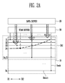
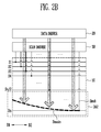
- FIG. 2A and 2B illustrate a data charge rate deviation
- the main scan lines Smain among the scan lines S1 to Sn, may be arranged in parallel.
- the main scan lines Smain may be connected to the pixels by a unit of line, and the sub-scan lines Ssub may electrically connect the main scan lines Smain with the driver 30.
- the main scan lines Smain may have the same length and the sub-scan lines Ssub may be arranged to be shorter toward the first direction D1. That is, the length of the scan lines S1 to Sn may get shorter toward the first direction D1, and get longer toward the second direction D2.
- the RC load of n/2 scan lines S1 to Sn/2 in which the main scan lines Smain are positioned at a first region DA1 at an upper side of the display unit 10, among n scan lines S1 to Sn may increase toward the second direction D2 since the scan signal is generally transmitted in a second direction D2 on the main scan lines Smain.
- a supply timing of the scan signal supplied to each pixel may be more delayed toward the second direction D2, so that a charge timing of a data voltage may be more delayed toward the second direction D2.
- a charge rate of the data voltage may be reduced as the pixels are positioned in the second direction D2 among the pixels connected to the same scan line.
- the RC load of the n/2 scan lines Sn/2+1 to Sn in which the main scan lines Smain may be positioned at a second region DA2 at the lower side of the display unit 10, among the n scan lines S1 to Sn may increase toward a first direction D1 since the scan signal is generally transmitted in the first direction D1 on the main scan lines Smain.
- the supply timing of the scan signal supplied to each pixel may be more delayed toward the first direction D1, so that the charge timing of the data voltage may be more delayed toward to the first direction D1. Accordingly, the charge rage of the data voltage may be reduced as the pixels are positioned in the first direction D1 among the pixels connected to the same scan line.
- each pixel may charge the data voltage corresponding to the data signal.
- a predetermined time may be required to charge the data voltage to a predetermined voltage level. It may be required to complete a charge of the data voltage within a 1 horizontal time (1H time) during which the scan signal is applied.
- the data signal output at the same time may be transmitted to the pixels simultaneously.
- each pixel may start charging the data voltage at the same time.
- the scan signal is not supplied to the pixels in the first row at the same time but at the different time, the pixels that receive the scan signals relatively late may start charging the data voltage late. Therefore, when the supply timings of the scan signal supplied to each pixel are different from each other, the data charge rate deviation may occur.
- the pixels positioned in the first direction D1 from the main scan line of the first scan line S1 may charge the data voltage relatively quickly.
- the pixels positioned in the second direction D2 may charge the data voltage relatively slowly.
- the pixels positioned in the second direction D2 from the main scan line of the n-th scan line Sn may charge the data voltage relatively quickly.
- the pixels positioned in the first direction D1 may charge the data voltage relatively slowly.
- the data charge rate deviation may occur between the pixels connected to the first scan line S1 and the pixels connected to the n-th scan line Sn. As a result, the display quality may be reduced due to the non-uniformity of the data charge rate between the pixels.
- FIG. 3 is a detailed diagram of a timing controller.
- FIGS. 4A and 4B illustrate the embodiments controlling the output timing of a data signal.
- the data driver 20 may be a plurality of data drivers, and each of the plurality of data drivers may supply a data signal to each of the data lines D1 to Dm.
- a first data driver 21 may be connected to a first group of the data lines D1 to Dm and supply the data signal whose output timing is controlled differently in response to a first data timing control signal DTCS1 of the data timing controller 40 to the first group of the data lines D1 to Dm.
- a second data driver 22 may be connected to a second group of the data lines D1 to Dm and supply the data signal whose output timing is controlled differently in response to a second data timing control signal DTCS2 of the data timing controller 40 to the second group of the data lines D1 to Dm.
- a third data driver 23 may be connected to a third group of the data lines D1 to Dm and supply the data signal whose output timing is controlled differently in response to a third data timing control signal DTCS3 of the data timing controller 40 to the third group of the data lines D1 to Dm.
- the timing controller 40 may include a plurality of line memories 41, 42 and 43 and a data timing controller 45.
- the plurality of line memories 41, 42 and 43 may temporarily store the image data DATA of a 1 horizontal line divided corresponding to the plurality of data drivers 21, 22 and 23.
- a first line memory 41 may store first image data DATA1 and output the first image data DATA1 to the first data driver 21;
- a second line memory 42 may store second image data DATA2 and output the second image data DATA2 to a second data driver 22;
- a third line memories 43 may store third image data DATA3 and output the third image data DATA3 to a third data driver 23.
- the plurality of line memories 41, 42 and 43 may control the output timing of the image data DATA by controlling of the data timing controller 45.
- the data timing controller 45 may generate data timing control signals DTCS1, DTCS2 and DTCS3 to control data drivers 21, 22 and 23 such that the data signal output corresponding to the scan signal is supplied at the different output timings within a 1 horizontal time (1H time). For example, with regard to m data lines, the data timing controller 45 may control the data drivers 21, 22 and 23 to control an output timing of the data signal at a 1 horizontal time/m interval.
- the data timing controller 45 may transmit scan line information SLD relating to the scan line to which the scan signal is supplied to the line memories 41, 42 and 43 in response to a data enable signal DE.
- the scan line information SLD may include information regarding which scan lines the scan signal is supplied, among the scan lines S1 to Sn, and output timing information of the data signal that is already determined for each of the scan lines S1 to Sn.
- the line memories 41, 42 and 43 may control the output timing of the first to third image data DATA1, DATA2 and DATA3 according to the scan line information SLD.
- the output timing of the image data may be determined in sequence of the third line memory 43, the second line memory 42 and the first line memory 41.
- the third image data DATA3 is supplied to the third data driver 23
- the second image data DATA2 is supplied to the second data driver 22
- the first image data DATA1 is supplied to the first data driver 21.
- the output timing of image data may be determined in sequence of the first line memory 41, the second line memory 42 and the third line memory 43.
- the first image data DATA1 is supplied to the first data driver 21
- the second image data DATA2 is supplied to the second data driver 22
- the third image data DATA3 is supplied to the third data driver 23.
- the data drivers 21, 22 and 23 may control the output timing of the data signal by changing a slew rate of the data signal output to each of the data lines D1 to Dm.
- FIGS. 4A and 4B illustrate the embodiments controlling an output timing of a data signal.
- the data timing controller 45 may control the data driver 20 to delay the output timing of the data signal supplied to the data lines positioned in a first direction D1 rather than a second direction D2, among the data lines D1 to Dm.
- the data timing controller 45 may delay the output timing of the data signal by a predetermined time.
- the data timing controller 45 may advance the output timing of the data signal by a predetermined time.
- the third data driver 23 may output the data signal at the 1 horizontal time/m interval during the first section t0 to t1, and subsequently, the second data driver 22 may output the data signal at the 1 horizontal time/m interval during the second section t1 to t2, the first data driver 21 may output the data signal at the 1 horizontal time/m interval during the third section t2 to t3.
- the data signal may be transferred relatively quickly to the pixels positioned in the second direction D2 and the data voltage may be charged.
- the data voltage may be charged relatively slowly into the pixels positioned in the first direction D1. Accordingly, the data charge rate deviation generated by an increase of a RC load to the second direction D2 may be reduced.
- the data timing controller 45 may control the data driver 20 to delay the output timing of the data signal supplied to the data lines positioned in the second direction D2 rather than the first direction D1. For example, while the scan signal is supplied to the n-th scan line Sn, the data voltage may be charged relatively quickly into the pixels positioned in the second direction D2. The data timing controller 45 may delay the output timing of the data signal by the predetermined time. On the other hand, since the data voltage may be charged relatively slowly into the pixels in the first direction D1, the data timing controller 45 may advance the output timing of the data signal by the predetermined time.
- the first data driver 21 may output the data signal by the 1 horizontal time/m interval during the first period t0 to t1; subsequently, the second data driver 22 may output the data signal by the 1 horizontal time /m interval during the second period t1 to t2; and next, third data driver 23 may output the data signal by the 1 horizontal time /m interval during the third period t2 to t3.
- the data signal is relatively quickly transferred to the pixels positioned in the first direction D1 and the data voltage may be charged.
- the data voltage may be charged relatively slowly in the pixels positioned in the second direction D2. Accordingly, the data charge rate deviation generated by an increase of RC load to the first direction D1 may be reduced.
- display quality since the output timing of the data signal is controlled according to the position of the scan line to which the scan signal is supplied, display quality may be improved by decreasing a data charging rate deviation according to a RC load difference of the scan lines.
Landscapes
- Engineering & Computer Science (AREA)
- Physics & Mathematics (AREA)
- Computer Hardware Design (AREA)
- General Physics & Mathematics (AREA)
- Theoretical Computer Science (AREA)
- Microelectronics & Electronic Packaging (AREA)
- Control Of Indicators Other Than Cathode Ray Tubes (AREA)
Abstract
Description
- The present invention relates to a display device.
- Among the display devices, a flat panel display that has excellent quality of screen, is light weight, and has low power consumption is frequently used. A display device may include a liquid crystal display, an organic light emitting display, etc. The display device may include a display unit in which a plurality of pixels are arranged in the matrix configuration, a scan driver supplying a scan signal, and a data driver supplying a data signal.
- The display device may have a structure in which the scan driver is arranged on one side of the display unit and the data driver is arranged on another side of the display unit. However, the display device utilized in a mobile device requires a narrow bezel having a minimized non-display region of both sides. In order to embody the narrow bezel, a panel in the formation of a single-side driving in which the scan driver and the data driver are arranged on one side has been studied.
- However, when the display device panel is in the formation of single-side driving, the scan lines have a different length from each other, and due to a wiring structure, lack of uniformity of RC load occurs, and a data charge rate deviation occurs. As a result, the display quality is reduced since a scan signal and a data signal are not supplied to pixels at an accurate timing.
- The present disclosure sets out to provide a display device capable of improving display quality by decreasing a data charge rate deviation.
- A display device according to an embodiment of the invention may include a display unit including a plurality of pixels connected with data lines and scan lines with different lengths; a data driver configured to supply a data signal to the data lines; a scan driver configured to supply a scan signal to the scan lines; and a timing controller configured to control the data driver to supply the data signal to the data lines at different output timings according to a position of a scan line to which the scan signal is supplied.
- The scan lines may include main scan lines connected to the pixels by row and sub-scan lines connecting the scan driver with the main scan lines. The data lines may be connected to the pixels by column. The data lines and the sub-scan lines may extend in parallel, and the sub-scan lines and the data lines may be arranged alternately with each other.
- The data driver may include a plurality of data drivers, and the timing controller may include a plurality of line memories configured to temporarily store image data corresponding to a 1 horizontal line divided corresponding to the plurality of data drivers. The timing controller may include a data timing controller configured to generate data timing control signals to control the data drivers to cause the data signal output corresponding to the scan signal to be supplied at the different output timings within a 1 horizontal time (1 H time).
- The data timing controller may control the data drivers to control an output timing of the data signal at an interval of the 1 horizontal time/m, m being a natural number corresponding to a count of the data lines. The data timing controller may be configured to transmit scan line information relating to the scan lines to which the scan signal is supplied to the line memories, and the line memories may be configured to control an output timing of the image data according to the scan line information.
- The main scan lines may have the same length, and lengths of the sub-scan lines may be reduced toward a first direction. The timing controller may be configured to control the data driver to delay an output timing of the data signal supplied to the data lines positioned in a first direction rather than the data lines in a second direction opposite to the first direction, among the data lines, when the scan signal is supplied to n/2 scan lines of which the sub-scan lines are relatively short, among n scan lines, and the timing controller may control the data driver to delay the output timing of the data signal supplied to the data lines positioned in the second direction rather than the data lines in the first direction when the scan signal is supplied to the other n/2 scan lines of which the sub-scan lines are relatively long, among the n scan lines.
- The data driver may be configured to control the output timing of the data signal by changing a slew rate of the data signal output to each of the data lines. The scan driver and the data driver may be arranged on one side of the display unit.
- At least some of the above and other features of the invention are set out in the claims.
- Example embodiments of the invention are now described more fully hereinafter with reference to the accompanying drawings; however, the invention may be embodied in different forms and should not be construed as limited to the embodiments set forth herein. Rather, these embodiments are provided to help convey the scope of the example embodiments to those skilled in the art.
- In the drawing figures, dimensions may be exaggerated for clarity of illustration. When an element is referred to as being "between" two elements, it may be the only element between the two elements, or one or more intervening elements may also be present. Like reference numerals refer to like elements throughout.
-
FIG. 1A is a schematic block diagram of a display device according to an embodiment of the invention; andFIG. 1B is a circuit diagram illustrating pixels of the display device as shown inFIG. 1A . -
FIG. 2A and2B illustrate a data charge rate deviation. -
FIG. 3 is a detailed block diagram of a timing controller; -
FIGS. 4A and 4B illustrate embodiments in which an output timing of a data signal is controlled. - Example embodiments of the invention are now described more fully hereinafter with reference to the accompanying drawings.
-
FIG. 1A is a schematic block diagram of a display device according to an embodiment of the invention; andFIG. 1B is a circuit diagram illustrating pixels of the display device as shown inFIG. 1A . - Referring to
FIG. 1A , a display device according to this embodiment may include adisplay unit 10, adata driver 20, ascan driver 30 and atiming controller 40. - The
display unit 10 may include a plurality of pixels connected to scan lines S1 to Sn and data lines D1 to Dm. The display device according to the embodiment may be a display device of single-side driving in which thedata driver 20 and thescan driver 30 are arranged on one side. Each of the scan lines S1 to Sn may include main scan lines Smain connected to the pixels by a row and sub-scan lines Ssub connecting thescan driver 30 with the main scan lines Smain. Since the distances between the main scan lines Smain and thescan driver 30 are different from each other, each of the sub-scan lines Ssub may have a different length. The data lines D1 to Dm may be connected to the pixels by column. - The data lines D1 to Dm and the sub-scan lines Ssub may be in parallel, and the sub-scan lines Ssub and the data lines D1 to Dm may be alternately arranged with each other. The main scan lines Smain may have the same length, and the sub-scan lines Ssub may be arranged to be shorter toward a first direction D1.
- The first direction D1 may be a left side, such as shown in
FIG. 1A . However, the invention is not limited to a wiring structure of the scan lines S1 to Sn. According to another embodiment, the sub-scan lines Ssub may be arranged to be shorter toward a second direction D2 that is the opposite to the first direction D1. The second direction D2 may be a right side, such as shown inFIG. 1A . - The pixels arranged in the matrix configuration in the
display unit 10 may receive a scan signal through the scan lines S1 to Sn, and a data signal through the data lines D1 to Dm. The pixels may emit light with brightness corresponding to the data signal supplied from the data lines D1 to Dm when the scan signal is supplied from the scan lines S1 to Sn. Thedisplay unit 10 according to the embodiment ofFIG. 1A may be a display unit of an organic light-emitting diode OLED. - Referring to
FIG. 1B , each pixel PX according to the embodiment may include the organic light-emitting diode OLED, and receive a high power voltage ELVDD and a low power voltage ELVSS from an external device. Further, the pixel PX may include a capacitor Cst, a first transistor T1, and a second transistor T2. As described above, the scan line Sn may include the main scan lines Smain directly connected to the pixel PX and the sub-scan line Ssub connecting thescan driver 30 with the main scan line Smain. However, the pixel PX included in the display device is not limited to the embodiment ofFIG. 1B . - Referring a driving method of the pixel PX, the scan signal having a gate-on level may be applied through the scan line Sn, and the first transistor T1 may be turned on. When the first transistor T1 is turned on, the data signal supplied through the data line Dm may be applied to a gate electrode and the capacitor Cst of the second transistor T2. While the data signal is supplied through the data line Dm, a data voltage corresponding to the data signal may be charged in the capacitor Cst. The second transistor may generate the driving current and output the driving current to the organic light-emitting diode OLED according to the data voltage. The organic light-emitting diode OLED may emit light with brightness corresponding to the driving current.
- The
data driver 20 may be connected to a plurality of data lines D1 to Dm, generate the data signal on the basis of a data control signal DCS and image data DATA' of thetiming controller 40, and output the generated data signal to the data lines D1 to Dm. The data control signal DCS may include a data timing control signal DTCS configured to control an output timing of the data signal. Thedata driver 20 may control the output timings of the data signal, which output to the data lines D1 to Dm differently from each other in response to the data timing control signal DTCS. In detail, the data signal supplied to the data lines D1 to Dm may be supplied to the pixels selected by a scan line when the scan signal is supplied. A data voltage corresponding to the data signal may be charged into the pixels. When the output timings of the data signal supplied to each pixel are different from each other, the data signal may be supplied to the pixels at different timings, and each data charge rage of the pixels may be controlled. - The
scan driver 30 may be connected to the plurality of scan lines S1 to Sn, and generate a scan signal in response to a scan control signal SCS of thetiming controller 40, and output the generated scan signal to the scan lines S1 to Sn sequentially. Thescanning driver 30 may be composed of the plurality of stage circuits, and when the scan signal is supplied to the scan lines S1 to Sn sequentially, the pixels may be selected by a unit of horizontal line. However, thescan driver 30 may perform an operation outputting an emitting control signal to the plurality of emitting control lines (not illustrated) connected with the pixels in addition to the scan signals. - The
scan driver 30 and thedata driver 20 may be arranged on one side of thedisplay unit 10. Thedata driver 20 may be arranged on one side of thedisplay unit 10 and thescan driver 30 may be arranged on another side opposite to the one side thereof. Therefore, thedisplay device 10 may include the narrow bezel with a minimized non-display region of both sides of thedisplay unit 10. - The
timing controller 40 may receive the image data DATA and a clock signal CLK to control a display thereof. Thetiming controller 40 may perform image processing of input image data DATA and generate the compensated image data DATA' to be suitable to an image display of thedisplay unit 10 and output the compensated image data DATA' to thedata driver 20. Further, thetiming controller 40 may generate and output driving control signals SCS and DCS configured to control the driving of thescan driver 30 and thedata driver 20 on the basis of the clock signal CLK. - The
timing controller 40 may control thedata driver 20 to supply the data signal to the data lines D1 to Dm at different timings according to the position of the scan lines to which the scan signal is supplied. In other words, the scan signal may not be supplied to all the scan lines S1 to Sn at the same time, but to each of the scan lines S1 to Sn sequentially. Thetiming controller 40 may determine the position of the scan line in thedisplay unit 10 to which the scan signal is supplied, and control thedata driver 20 to cause the data signal, which is synchronized to the timing when the scan signal is supplied, to be output to the data lines D1 to Dm at different timings, that is, not at the same time. To this end, thetiming controller 40 may generate the data timing control signal DTCS to control the output timing of the data signal. The specific description of thetiming controller 40 is described with reference toFIG. 3 . -
FIG. 2A and2B illustrate a data charge rate deviation. - Referring to
FIG. 2A and2B , the main scan lines Smain, among the scan lines S1 to Sn, may be arranged in parallel. The sub-scan lines Ssub and the data lines D1 to Dm, among the scan lines S1 to Sn, may be arranged vertically. The main scan lines Smain may be connected to the pixels by a unit of line, and the sub-scan lines Ssub may electrically connect the main scan lines Smain with thedriver 30. The main scan lines Smain may have the same length and the sub-scan lines Ssub may be arranged to be shorter toward the first direction D1. That is, the length of the scan lines S1 to Sn may get shorter toward the first direction D1, and get longer toward the second direction D2. - In the wiring structure, the RC load of n/2 scan lines S1 to Sn/2 in which the main scan lines Smain are positioned at a first region DA1 at an upper side of the
display unit 10, among n scan lines S1 to Sn, may increase toward the second direction D2 since the scan signal is generally transmitted in a second direction D2 on the main scan lines Smain. In this case, a supply timing of the scan signal supplied to each pixel may be more delayed toward the second direction D2, so that a charge timing of a data voltage may be more delayed toward the second direction D2. Accordingly, a charge rate of the data voltage may be reduced as the pixels are positioned in the second direction D2 among the pixels connected to the same scan line. - On the other hand, the RC load of the n/2 scan lines Sn/2+1 to Sn in which the main scan lines Smain may be positioned at a second region DA2 at the lower side of the
display unit 10, among the n scan lines S1 to Sn, may increase toward a first direction D1 since the scan signal is generally transmitted in the first direction D1 on the main scan lines Smain. In this case, the supply timing of the scan signal supplied to each pixel may be more delayed toward the first direction D1, so that the charge timing of the data voltage may be more delayed toward to the first direction D1. Accordingly, the charge rage of the data voltage may be reduced as the pixels are positioned in the first direction D1 among the pixels connected to the same scan line. - In detail, each pixel may charge the data voltage corresponding to the data signal. A predetermined time may be required to charge the data voltage to a predetermined voltage level. It may be required to complete a charge of the data voltage within a 1 horizontal time (1H time) during which the scan signal is applied. When the pixels are in the same row, the data signal output at the same time may be transmitted to the pixels simultaneously. When the scan signal is supplied to the pixels in a first row, each pixel may start charging the data voltage at the same time. However, when the scan signal is not supplied to the pixels in the first row at the same time but at the different time, the pixels that receive the scan signals relatively late may start charging the data voltage late. Therefore, when the supply timings of the scan signal supplied to each pixel are different from each other, the data charge rate deviation may occur.
- For example, in the case of a first scan line S1, the pixels positioned in the first direction D1 from the main scan line of the first scan line S1 may charge the data voltage relatively quickly. However, the pixels positioned in the second direction D2 may charge the data voltage relatively slowly. In the case of the n-th scan line Sn, the pixels positioned in the second direction D2 from the main scan line of the n-th scan line Sn may charge the data voltage relatively quickly. However, the pixels positioned in the first direction D1 may charge the data voltage relatively slowly. Further, the data charge rate deviation may occur between the pixels connected to the first scan line S1 and the pixels connected to the n-th scan line Sn. As a result, the display quality may be reduced due to the non-uniformity of the data charge rate between the pixels.
-
FIG. 3 is a detailed diagram of a timing controller.FIGS. 4A and 4B illustrate the embodiments controlling the output timing of a data signal. - Referring to
FIG. 3 , thedata driver 20 according to the embodiment may be a plurality of data drivers, and each of the plurality of data drivers may supply a data signal to each of the data lines D1 to Dm. For example, afirst data driver 21 may be connected to a first group of the data lines D1 to Dm and supply the data signal whose output timing is controlled differently in response to a first data timing control signal DTCS1 of thedata timing controller 40 to the first group of the data lines D1 to Dm. Asecond data driver 22 may be connected to a second group of the data lines D1 to Dm and supply the data signal whose output timing is controlled differently in response to a second data timing control signal DTCS2 of thedata timing controller 40 to the second group of the data lines D1 to Dm. Athird data driver 23 may be connected to a third group of the data lines D1 to Dm and supply the data signal whose output timing is controlled differently in response to a third data timing control signal DTCS3 of thedata timing controller 40 to the third group of the data lines D1 to Dm. - The
timing controller 40 may include a plurality ofline memories data timing controller 45. The plurality ofline memories data drivers first line memory 41 may store first image data DATA1 and output the first image data DATA1 to thefirst data driver 21; asecond line memory 42 may store second image data DATA2 and output the second image data DATA2 to asecond data driver 22; and athird line memories 43 may store third image data DATA3 and output the third image data DATA3 to athird data driver 23. The plurality ofline memories data timing controller 45. - The
data timing controller 45 may generate data timing control signals DTCS1, DTCS2 and DTCS3 to controldata drivers data timing controller 45 may control thedata drivers - Further, the
data timing controller 45 may transmit scan line information SLD relating to the scan line to which the scan signal is supplied to theline memories line memories - For example, when the scan signal is supplied to the first scan line S1, the output timing of the image data may be determined in sequence of the
third line memory 43, thesecond line memory 42 and thefirst line memory 41. In other words, after the third image data DATA3 is supplied to thethird data driver 23, the second image data DATA2 is supplied to thesecond data driver 22, and the first image data DATA1 is supplied to thefirst data driver 21. When the scan signal is supplied to the n-th scan line Sn, the output timing of image data may be determined in sequence of thefirst line memory 41, thesecond line memory 42 and thethird line memory 43. In other words, after the first image data DATA1 is supplied to thefirst data driver 21, the second image data DATA2 is supplied to thesecond data driver 22, and the third image data DATA3 is supplied to thethird data driver 23. - Further, the
data drivers -
FIGS. 4A and 4B illustrate the embodiments controlling an output timing of a data signal. - Referring to
FIG. 4A , when it is considered that a scan signal may be supplied to n/2 scan lines S1 to Sn/2 in which the sub-scan lines Ssub are relatively short, among the n scan lines S1 to Sn, thedata timing controller 45 may control thedata driver 20 to delay the output timing of the data signal supplied to the data lines positioned in a first direction D1 rather than a second direction D2, among the data lines D1 to Dm. For example, while the scan signal is supplied to the first scan line S1, the data voltage may be charged relatively rapidly in the pixels positioned in the first direction D1. Therefore, thedata timing controller 45 may delay the output timing of the data signal by a predetermined time. On the other hand, since the data voltage may be charged relatively slowly in the pixels positioned in the second direction D2, thedata timing controller 45 may advance the output timing of the data signal by a predetermined time. - When the supply period is divided into a first section t0 to t1, a second section t1 to t2 after the first section t0 to t1, and a third section t2 to t3 after the second section t1 to t2 on the basis of a supply starting point t0 of the scan signal, the
third data driver 23 may output the data signal at the 1 horizontal time/m interval during the first section t0 to t1, and subsequently, thesecond data driver 22 may output the data signal at the 1 horizontal time/m interval during the second section t1 to t2, thefirst data driver 21 may output the data signal at the 1 horizontal time/m interval during the third section t2 to t3. As a result, the data signal may be transferred relatively quickly to the pixels positioned in the second direction D2 and the data voltage may be charged. However, the data voltage may be charged relatively slowly into the pixels positioned in the first direction D1. Accordingly, the data charge rate deviation generated by an increase of a RC load to the second direction D2 may be reduced. - Referring to
FIG. 4B , when it is considered that the scan signal may be supplied to the n/2 scan lines Sn/2+1 to Sn in which the sub-scan lines Ssub are relatively long, among the n scan lines S1 to Sn, thedata timing controller 45 may control thedata driver 20 to delay the output timing of the data signal supplied to the data lines positioned in the second direction D2 rather than the first direction D1. For example, while the scan signal is supplied to the n-th scan line Sn, the data voltage may be charged relatively quickly into the pixels positioned in the second direction D2. Thedata timing controller 45 may delay the output timing of the data signal by the predetermined time. On the other hand, since the data voltage may be charged relatively slowly into the pixels in the first direction D1, thedata timing controller 45 may advance the output timing of the data signal by the predetermined time. - The
first data driver 21 may output the data signal by the 1 horizontal time/m interval during the first period t0 to t1; subsequently, thesecond data driver 22 may output the data signal by the 1 horizontal time /m interval during the second period t1 to t2; and next,third data driver 23 may output the data signal by the 1 horizontal time /m interval during the third period t2 to t3. As a result, the data signal is relatively quickly transferred to the pixels positioned in the first direction D1 and the data voltage may be charged. However, the data voltage may be charged relatively slowly in the pixels positioned in the second direction D2. Accordingly, the data charge rate deviation generated by an increase of RC load to the first direction D1 may be reduced. - According to the present invention, since the output timing of the data signal is controlled according to the position of the scan line to which the scan signal is supplied, display quality may be improved by decreasing a data charging rate deviation according to a RC load difference of the scan lines.
- Example embodiments of the invention have been disclosed herein, and although specific terms are employed, they are used and are to be interpreted in a generic and descriptive sense only and not for purpose of limitation. In some instances, as would be apparent to one of ordinary skill in the art as of the filing of the present application, features, characteristics, and/or elements described in connection with a particular embodiment may be used singly or in combination with features, characteristics, and/or elements described in connection with other embodiments unless otherwise specifically indicated. Accordingly, those of skill in the art would understand that various changes in form and details may be made without departing from the scope of the following claims.
Claims (12)
- A display device, comprising:a display unit including a plurality of pixels connected with data lines and scan lines with different lengths;a data driver configured to supply a data signal to the data lines;a scan driver configured to supply a scan signal to the scan lines; anda timing controller configured to control the data driver to supply the data signal to the data lines at different output timings according to a position of a scan line to which the scan signal is supplied.
- A display device according to claim 1, wherein the scan lines include main scan lines connected to the pixels by row and sub-scan lines connecting the scan driver with the main scan lines.
- A display device according to claim 2, wherein the data lines are connected to the pixels by column.
- A display device according to claim 3, wherein the data lines and the sub-scan lines extend in parallel, and the sub-scan lines and the data lines are arranged alternately with each other.
- A display device of claim 3 or 4, wherein the data driver includes a plurality of data drivers, and
the timing controller includes a plurality of line memories configured to temporarily store image data corresponding to a 1 horizontal line divided corresponding to the plurality of data drivers. - A display device according to claim 5, wherein the timing controller includes a data timing controller configured to generate data timing control signals to control the data drivers to cause the data signal output corresponding to the scan signal to be supplied at the different output timings within a 1 horizontal time (1 H time).
- A display device according to claim 6, wherein the data timing controller is configured to control the data drivers to control an output timing of the data signal at an interval of the 1 horizontal time/m, m being a natural number corresponding to a count of the data lines.
- A display device according to claim 6, wherein the data timing controller is configured to transmit scan line information relating to the scan lines to which the scan signal is supplied to the line memories, and
the line memories are configured to control an output timing of the image data according to the scan line information. - A display device according to claim 3, wherein the main scan lines have the same length, and
lengths of the sub-scan lines are reduced toward a first direction. - A display device according to claim 9, wherein the timing controller is configured to control the data driver to delay an output timing of the data signal supplied to the data lines positioned in a first direction rather than the data lines in a second direction opposite to the first direction, among the data lines, when the scan signal is supplied to n/2 scan lines of which the sub-scan lines are relatively short, among n scan lines, and
the timing controller is configured to control the data driver to delay the output timing of the data signal supplied to the data lines positioned in the second direction rather than the data lines in the first direction when the scan signal is supplied to the other n/2 scan lines of which the sub-scan lines are relatively long, among the n scan lines. - A display device according to claim 10, wherein the data driver is configured to control the output timing of the data signal by changing a slew rate of the data signal output to each of the data lines.
- A display device according to any preceding claim, wherein the scan driver and the data driver are arranged on one side of the display unit.
Applications Claiming Priority (1)
| Application Number | Priority Date | Filing Date | Title |
|---|---|---|---|
| KR1020150112594A KR102344502B1 (en) | 2015-08-10 | 2015-08-10 | Display device |
Publications (2)
| Publication Number | Publication Date |
|---|---|
| EP3131086A1 true EP3131086A1 (en) | 2017-02-15 |
| EP3131086B1 EP3131086B1 (en) | 2019-01-09 |
Family
ID=56618083
Family Applications (1)
| Application Number | Title | Priority Date | Filing Date |
|---|---|---|---|
| EP16183599.6A Active EP3131086B1 (en) | 2015-08-10 | 2016-08-10 | Display device |
Country Status (4)
| Country | Link |
|---|---|
| US (1) | US10417970B2 (en) |
| EP (1) | EP3131086B1 (en) |
| KR (1) | KR102344502B1 (en) |
| CN (1) | CN106448551B (en) |
Cited By (5)
| Publication number | Priority date | Publication date | Assignee | Title |
|---|---|---|---|---|
| CN114267275A (en) * | 2020-09-16 | 2022-04-01 | 三星显示有限公司 | Display device with scanning signal with adjustable pulse width |
| EP3996079A1 (en) * | 2020-11-10 | 2022-05-11 | Samsung Display Co., Ltd. | Data driving circuit and a display device including the same |
| CN115881027A (en) * | 2021-09-28 | 2023-03-31 | 乐金显示有限公司 | Display device and driving method of the same |
| CN116386539A (en) * | 2021-12-30 | 2023-07-04 | 乐金显示有限公司 | display device |
| US12112719B2 (en) | 2022-03-04 | 2024-10-08 | Innolux Corporation | Electronic device and modulating device with short frame time length |
Families Citing this family (14)
| Publication number | Priority date | Publication date | Assignee | Title |
|---|---|---|---|---|
| US10410599B2 (en) * | 2015-08-13 | 2019-09-10 | Samsung Electronics Co., Ltd. | Source driver integrated circuit for ompensating for display fan-out and display system including the same |
| TWI642305B (en) * | 2017-05-10 | 2018-11-21 | 友達光電股份有限公司 | Display panel |
| CN107492353B (en) * | 2017-07-21 | 2019-06-11 | 惠科股份有限公司 | Driving method and driving device of display panel |
| KR102715306B1 (en) * | 2019-04-19 | 2024-10-14 | 삼성디스플레이 주식회사 | Source driver and display device having the same |
| US11145269B2 (en) | 2019-08-02 | 2021-10-12 | Sakai Display Products Corporation | Display apparatus accurately reducing display non-uniformity |
| KR102651717B1 (en) * | 2020-01-07 | 2024-03-27 | 삼성디스플레이 주식회사 | Display device |
| KR102863099B1 (en) * | 2020-08-14 | 2025-09-25 | 삼성디스플레이 주식회사 | Display device |
| KR102744638B1 (en) * | 2020-08-19 | 2024-12-23 | 삼성디스플레이 주식회사 | Method for compensating mura of display device and mura compensation system |
| KR102912675B1 (en) * | 2020-09-08 | 2026-01-15 | 삼성디스플레이 주식회사 | Display device |
| KR102814643B1 (en) * | 2020-09-14 | 2025-06-02 | 삼성디스플레이 주식회사 | Display device and method for driving the same |
| KR102768805B1 (en) | 2020-10-19 | 2025-02-19 | 삼성디스플레이 주식회사 | Display apparatus |
| US12154506B2 (en) * | 2020-12-04 | 2024-11-26 | Sharp Kabushiki Kaisha | Display device and pixel circuit |
| CN113972224B (en) * | 2021-10-21 | 2024-12-20 | 昆山国显光电有限公司 | Display panel and display device |
| CN119763476B (en) * | 2025-02-19 | 2025-10-24 | 京东方科技集团股份有限公司 | Display panel, driving method thereof, and display device |
Citations (3)
| Publication number | Priority date | Publication date | Assignee | Title |
|---|---|---|---|---|
| US20070152947A1 (en) * | 2005-12-22 | 2007-07-05 | Yasuhiro Tanaka | Display apparatus |
| US20140375922A1 (en) * | 2013-06-19 | 2014-12-25 | Lg Display Co., Ltd. | Liquid crystal display device and method of driving the same |
| EP3046102A1 (en) * | 2015-01-13 | 2016-07-20 | Samsung Display Co., Ltd. | Display apparatus and method of driving display panel using the same |
Family Cites Families (15)
| Publication number | Priority date | Publication date | Assignee | Title |
|---|---|---|---|---|
| JP2000214816A (en) * | 1999-01-21 | 2000-08-04 | Sharp Corp | Display device control circuit and control method |
| US7142186B2 (en) * | 2003-03-24 | 2006-11-28 | Hivix Co., Ltd | Method and apparatus for converting gradation data in STN LCD |
| KR20060093829A (en) * | 2005-02-22 | 2006-08-28 | 삼성전자주식회사 | Liquid crystal display |
| JP4659885B2 (en) * | 2006-11-21 | 2011-03-30 | シャープ株式会社 | Active matrix substrate, display panel, and display device |
| JP5186913B2 (en) * | 2007-01-22 | 2013-04-24 | セイコーエプソン株式会社 | Source driver, electro-optical device and electronic apparatus |
| CN101963724B (en) * | 2009-07-22 | 2012-07-18 | 北京京东方光电科技有限公司 | Liquid crystal display driving device |
| WO2011078168A1 (en) * | 2009-12-24 | 2011-06-30 | シャープ株式会社 | Liquid crystal display device |
| KR101633413B1 (en) * | 2009-12-31 | 2016-06-27 | 삼성디스플레이 주식회사 | Display panel and display apparatus having the same |
| KR101717076B1 (en) | 2010-11-20 | 2017-03-17 | 엘지디스플레이 주식회사 | Narrow bezel type array substrate and liquid crystal display device using the same |
| US9646559B2 (en) * | 2012-08-10 | 2017-05-09 | Lg Display Co., Ltd. | Liquid crystal display device |
| KR101991674B1 (en) * | 2012-08-10 | 2019-06-25 | 엘지디스플레이 주식회사 | Liquid crystal display device |
| CN103198803B (en) * | 2013-03-27 | 2016-08-10 | 京东方科技集团股份有限公司 | The driving control unit of a kind of display base plate, drive circuit and driving control method |
| KR102056674B1 (en) | 2013-06-28 | 2019-12-17 | 엘지디스플레이 주식회사 | Gate shift register and method for driving the same |
| JP6231314B2 (en) * | 2013-07-16 | 2017-11-15 | シナプティクス・ジャパン合同会社 | Display drive device |
| CN103745694A (en) * | 2013-11-27 | 2014-04-23 | 深圳市华星光电技术有限公司 | Driving method and driving circuit of display panel |
-
2015
- 2015-08-10 KR KR1020150112594A patent/KR102344502B1/en active Active
-
2016
- 2016-08-05 US US15/230,279 patent/US10417970B2/en active Active
- 2016-08-10 CN CN201610649482.2A patent/CN106448551B/en active Active
- 2016-08-10 EP EP16183599.6A patent/EP3131086B1/en active Active
Patent Citations (3)
| Publication number | Priority date | Publication date | Assignee | Title |
|---|---|---|---|---|
| US20070152947A1 (en) * | 2005-12-22 | 2007-07-05 | Yasuhiro Tanaka | Display apparatus |
| US20140375922A1 (en) * | 2013-06-19 | 2014-12-25 | Lg Display Co., Ltd. | Liquid crystal display device and method of driving the same |
| EP3046102A1 (en) * | 2015-01-13 | 2016-07-20 | Samsung Display Co., Ltd. | Display apparatus and method of driving display panel using the same |
Cited By (10)
| Publication number | Priority date | Publication date | Assignee | Title |
|---|---|---|---|---|
| CN114267275A (en) * | 2020-09-16 | 2022-04-01 | 三星显示有限公司 | Display device with scanning signal with adjustable pulse width |
| EP3996079A1 (en) * | 2020-11-10 | 2022-05-11 | Samsung Display Co., Ltd. | Data driving circuit and a display device including the same |
| KR20220063870A (en) * | 2020-11-10 | 2022-05-18 | 삼성디스플레이 주식회사 | Data driving circuit and display device including the same |
| US11538384B2 (en) | 2020-11-10 | 2022-12-27 | Samsung Display Co., Ltd. | Data driving circuit and a display device including the same |
| US11908365B2 (en) | 2020-11-10 | 2024-02-20 | Samsung Display Co., Ltd. | Data driving circuit and a display device including the same |
| CN115881027A (en) * | 2021-09-28 | 2023-03-31 | 乐金显示有限公司 | Display device and driving method of the same |
| US12100338B2 (en) | 2021-09-28 | 2024-09-24 | Lg Display Co., Ltd. | Display device and driving method of the same |
| CN116386539A (en) * | 2021-12-30 | 2023-07-04 | 乐金显示有限公司 | display device |
| US12557504B2 (en) | 2021-12-30 | 2026-02-17 | Lg Display Co., Ltd | Display apparatus |
| US12112719B2 (en) | 2022-03-04 | 2024-10-08 | Innolux Corporation | Electronic device and modulating device with short frame time length |
Also Published As
| Publication number | Publication date |
|---|---|
| CN106448551A (en) | 2017-02-22 |
| KR102344502B1 (en) | 2021-12-30 |
| CN106448551B (en) | 2021-03-16 |
| US20170047016A1 (en) | 2017-02-16 |
| EP3131086B1 (en) | 2019-01-09 |
| US10417970B2 (en) | 2019-09-17 |
| KR20170019021A (en) | 2017-02-21 |
Similar Documents
| Publication | Publication Date | Title |
|---|---|---|
| EP3131086B1 (en) | Display device | |
| US10366651B2 (en) | Organic light-emitting display device and driving method thereof | |
| US10699645B2 (en) | Simplified gate driver configuration and display device including the same | |
| US9812062B2 (en) | Display apparatus and method of driving the same | |
| US9552774B2 (en) | Organic light emitting display device including data distribution unit and driving method thereof | |
| KR101142729B1 (en) | Pixel and Organic Light Emitting Display Device Using the same | |
| US9406261B2 (en) | Stage circuit and scan driver using the same | |
| US20160189600A1 (en) | Data control circuit and flat panel display device including the same | |
| US10878749B2 (en) | Display device and driving method thereof | |
| US8497855B2 (en) | Scan driving apparatus and driving method for the same | |
| KR102215244B1 (en) | Pixel circuit, driving method, and display apparatus having the same | |
| US11114039B2 (en) | Micro-display device and method of driving same | |
| KR102028995B1 (en) | Organic light emitting diode display device and method for driving the same | |
| KR100645698B1 (en) | Pixel, light emitting display device and driving method thereof | |
| CN108281115B (en) | Display device, display panel, driving method and gate driver circuit | |
| KR102244075B1 (en) | Apparatus for scan driving and display apparatus using thereof | |
| KR102527222B1 (en) | Display apparatus | |
| US10372002B2 (en) | Display device | |
| KR20150049121A (en) | Display deviceand and method for driving thereof | |
| US10242626B2 (en) | Stage and organic light emitting display device using the same | |
| CN113129826A (en) | Organic light emitting diode display device and driving method thereof | |
| EP2793215A1 (en) | Scan driver and organic light emitting display device including the same | |
| KR102223901B1 (en) | Display Device | |
| KR102199490B1 (en) | Emission control driver and organic light emitting display device having the same | |
| KR102457161B1 (en) | Display panel with integrated gate driver and display apparatus using the same |
Legal Events
| Date | Code | Title | Description |
|---|---|---|---|
| PUAI | Public reference made under article 153(3) epc to a published international application that has entered the european phase |
Free format text: ORIGINAL CODE: 0009012 |
|
| STAA | Information on the status of an ep patent application or granted ep patent |
Free format text: STATUS: THE APPLICATION HAS BEEN PUBLISHED |
|
| AK | Designated contracting states |
Kind code of ref document: A1 Designated state(s): AL AT BE BG CH CY CZ DE DK EE ES FI FR GB GR HR HU IE IS IT LI LT LU LV MC MK MT NL NO PL PT RO RS SE SI SK SM TR |
|
| AX | Request for extension of the european patent |
Extension state: BA ME |
|
| STAA | Information on the status of an ep patent application or granted ep patent |
Free format text: STATUS: REQUEST FOR EXAMINATION WAS MADE |
|
| 17P | Request for examination filed |
Effective date: 20170727 |
|
| RBV | Designated contracting states (corrected) |
Designated state(s): AL AT BE BG CH CY CZ DE DK EE ES FI FR GB GR HR HU IE IS IT LI LT LU LV MC MK MT NL NO PL PT RO RS SE SI SK SM TR |
|
| GRAP | Despatch of communication of intention to grant a patent |
Free format text: ORIGINAL CODE: EPIDOSNIGR1 |
|
| STAA | Information on the status of an ep patent application or granted ep patent |
Free format text: STATUS: GRANT OF PATENT IS INTENDED |
|
| INTG | Intention to grant announced |
Effective date: 20180718 |
|
| GRAS | Grant fee paid |
Free format text: ORIGINAL CODE: EPIDOSNIGR3 |
|
| GRAA | (expected) grant |
Free format text: ORIGINAL CODE: 0009210 |
|
| STAA | Information on the status of an ep patent application or granted ep patent |
Free format text: STATUS: THE PATENT HAS BEEN GRANTED |
|
| AK | Designated contracting states |
Kind code of ref document: B1 Designated state(s): AL AT BE BG CH CY CZ DE DK EE ES FI FR GB GR HR HU IE IS IT LI LT LU LV MC MK MT NL NO PL PT RO RS SE SI SK SM TR |
|
| REG | Reference to a national code |
Ref country code: GB Ref legal event code: FG4D |
|
| REG | Reference to a national code |
Ref country code: CH Ref legal event code: EP Ref country code: AT Ref legal event code: REF Ref document number: 1088285 Country of ref document: AT Kind code of ref document: T Effective date: 20190115 |
|
| REG | Reference to a national code |
Ref country code: DE Ref legal event code: R096 Ref document number: 602016009137 Country of ref document: DE |
|
| REG | Reference to a national code |
Ref country code: IE Ref legal event code: FG4D |
|
| REG | Reference to a national code |
Ref country code: NL Ref legal event code: MP Effective date: 20190109 |
|
| REG | Reference to a national code |
Ref country code: LT Ref legal event code: MG4D |
|
| PG25 | Lapsed in a contracting state [announced via postgrant information from national office to epo] |
Ref country code: NL Free format text: LAPSE BECAUSE OF FAILURE TO SUBMIT A TRANSLATION OF THE DESCRIPTION OR TO PAY THE FEE WITHIN THE PRESCRIBED TIME-LIMIT Effective date: 20190109 |
|
| REG | Reference to a national code |
Ref country code: AT Ref legal event code: MK05 Ref document number: 1088285 Country of ref document: AT Kind code of ref document: T Effective date: 20190109 |
|
| PG25 | Lapsed in a contracting state [announced via postgrant information from national office to epo] |
Ref country code: PL Free format text: LAPSE BECAUSE OF FAILURE TO SUBMIT A TRANSLATION OF THE DESCRIPTION OR TO PAY THE FEE WITHIN THE PRESCRIBED TIME-LIMIT Effective date: 20190109 Ref country code: SE Free format text: LAPSE BECAUSE OF FAILURE TO SUBMIT A TRANSLATION OF THE DESCRIPTION OR TO PAY THE FEE WITHIN THE PRESCRIBED TIME-LIMIT Effective date: 20190109 Ref country code: ES Free format text: LAPSE BECAUSE OF FAILURE TO SUBMIT A TRANSLATION OF THE DESCRIPTION OR TO PAY THE FEE WITHIN THE PRESCRIBED TIME-LIMIT Effective date: 20190109 Ref country code: LT Free format text: LAPSE BECAUSE OF FAILURE TO SUBMIT A TRANSLATION OF THE DESCRIPTION OR TO PAY THE FEE WITHIN THE PRESCRIBED TIME-LIMIT Effective date: 20190109 Ref country code: NO Free format text: LAPSE BECAUSE OF FAILURE TO SUBMIT A TRANSLATION OF THE DESCRIPTION OR TO PAY THE FEE WITHIN THE PRESCRIBED TIME-LIMIT Effective date: 20190409 Ref country code: PT Free format text: LAPSE BECAUSE OF FAILURE TO SUBMIT A TRANSLATION OF THE DESCRIPTION OR TO PAY THE FEE WITHIN THE PRESCRIBED TIME-LIMIT Effective date: 20190509 Ref country code: FI Free format text: LAPSE BECAUSE OF FAILURE TO SUBMIT A TRANSLATION OF THE DESCRIPTION OR TO PAY THE FEE WITHIN THE PRESCRIBED TIME-LIMIT Effective date: 20190109 |
|
| PG25 | Lapsed in a contracting state [announced via postgrant information from national office to epo] |
Ref country code: GR Free format text: LAPSE BECAUSE OF FAILURE TO SUBMIT A TRANSLATION OF THE DESCRIPTION OR TO PAY THE FEE WITHIN THE PRESCRIBED TIME-LIMIT Effective date: 20190410 Ref country code: IS Free format text: LAPSE BECAUSE OF FAILURE TO SUBMIT A TRANSLATION OF THE DESCRIPTION OR TO PAY THE FEE WITHIN THE PRESCRIBED TIME-LIMIT Effective date: 20190509 Ref country code: LV Free format text: LAPSE BECAUSE OF FAILURE TO SUBMIT A TRANSLATION OF THE DESCRIPTION OR TO PAY THE FEE WITHIN THE PRESCRIBED TIME-LIMIT Effective date: 20190109 Ref country code: BG Free format text: LAPSE BECAUSE OF FAILURE TO SUBMIT A TRANSLATION OF THE DESCRIPTION OR TO PAY THE FEE WITHIN THE PRESCRIBED TIME-LIMIT Effective date: 20190409 Ref country code: RS Free format text: LAPSE BECAUSE OF FAILURE TO SUBMIT A TRANSLATION OF THE DESCRIPTION OR TO PAY THE FEE WITHIN THE PRESCRIBED TIME-LIMIT Effective date: 20190109 Ref country code: HR Free format text: LAPSE BECAUSE OF FAILURE TO SUBMIT A TRANSLATION OF THE DESCRIPTION OR TO PAY THE FEE WITHIN THE PRESCRIBED TIME-LIMIT Effective date: 20190109 |
|
| REG | Reference to a national code |
Ref country code: DE Ref legal event code: R097 Ref document number: 602016009137 Country of ref document: DE |
|
| PG25 | Lapsed in a contracting state [announced via postgrant information from national office to epo] |
Ref country code: AL Free format text: LAPSE BECAUSE OF FAILURE TO SUBMIT A TRANSLATION OF THE DESCRIPTION OR TO PAY THE FEE WITHIN THE PRESCRIBED TIME-LIMIT Effective date: 20190109 Ref country code: SK Free format text: LAPSE BECAUSE OF FAILURE TO SUBMIT A TRANSLATION OF THE DESCRIPTION OR TO PAY THE FEE WITHIN THE PRESCRIBED TIME-LIMIT Effective date: 20190109 Ref country code: AT Free format text: LAPSE BECAUSE OF FAILURE TO SUBMIT A TRANSLATION OF THE DESCRIPTION OR TO PAY THE FEE WITHIN THE PRESCRIBED TIME-LIMIT Effective date: 20190109 Ref country code: DK Free format text: LAPSE BECAUSE OF FAILURE TO SUBMIT A TRANSLATION OF THE DESCRIPTION OR TO PAY THE FEE WITHIN THE PRESCRIBED TIME-LIMIT Effective date: 20190109 Ref country code: IT Free format text: LAPSE BECAUSE OF FAILURE TO SUBMIT A TRANSLATION OF THE DESCRIPTION OR TO PAY THE FEE WITHIN THE PRESCRIBED TIME-LIMIT Effective date: 20190109 Ref country code: CZ Free format text: LAPSE BECAUSE OF FAILURE TO SUBMIT A TRANSLATION OF THE DESCRIPTION OR TO PAY THE FEE WITHIN THE PRESCRIBED TIME-LIMIT Effective date: 20190109 Ref country code: RO Free format text: LAPSE BECAUSE OF FAILURE TO SUBMIT A TRANSLATION OF THE DESCRIPTION OR TO PAY THE FEE WITHIN THE PRESCRIBED TIME-LIMIT Effective date: 20190109 Ref country code: EE Free format text: LAPSE BECAUSE OF FAILURE TO SUBMIT A TRANSLATION OF THE DESCRIPTION OR TO PAY THE FEE WITHIN THE PRESCRIBED TIME-LIMIT Effective date: 20190109 |
|
| PLBE | No opposition filed within time limit |
Free format text: ORIGINAL CODE: 0009261 |
|
| STAA | Information on the status of an ep patent application or granted ep patent |
Free format text: STATUS: NO OPPOSITION FILED WITHIN TIME LIMIT |
|
| 26N | No opposition filed |
Effective date: 20191010 |
|
| PG25 | Lapsed in a contracting state [announced via postgrant information from national office to epo] |
Ref country code: SI Free format text: LAPSE BECAUSE OF FAILURE TO SUBMIT A TRANSLATION OF THE DESCRIPTION OR TO PAY THE FEE WITHIN THE PRESCRIBED TIME-LIMIT Effective date: 20190109 |
|
| PG25 | Lapsed in a contracting state [announced via postgrant information from national office to epo] |
Ref country code: TR Free format text: LAPSE BECAUSE OF FAILURE TO SUBMIT A TRANSLATION OF THE DESCRIPTION OR TO PAY THE FEE WITHIN THE PRESCRIBED TIME-LIMIT Effective date: 20190109 |
|
| PG25 | Lapsed in a contracting state [announced via postgrant information from national office to epo] |
Ref country code: MC Free format text: LAPSE BECAUSE OF FAILURE TO SUBMIT A TRANSLATION OF THE DESCRIPTION OR TO PAY THE FEE WITHIN THE PRESCRIBED TIME-LIMIT Effective date: 20190109 Ref country code: LU Free format text: LAPSE BECAUSE OF NON-PAYMENT OF DUE FEES Effective date: 20190810 Ref country code: LI Free format text: LAPSE BECAUSE OF NON-PAYMENT OF DUE FEES Effective date: 20190831 Ref country code: CH Free format text: LAPSE BECAUSE OF NON-PAYMENT OF DUE FEES Effective date: 20190831 |
|
| REG | Reference to a national code |
Ref country code: BE Ref legal event code: MM Effective date: 20190831 |
|
| PG25 | Lapsed in a contracting state [announced via postgrant information from national office to epo] |
Ref country code: IE Free format text: LAPSE BECAUSE OF NON-PAYMENT OF DUE FEES Effective date: 20190810 |
|
| PG25 | Lapsed in a contracting state [announced via postgrant information from national office to epo] |
Ref country code: BE Free format text: LAPSE BECAUSE OF NON-PAYMENT OF DUE FEES Effective date: 20190831 |
|
| PG25 | Lapsed in a contracting state [announced via postgrant information from national office to epo] |
Ref country code: CY Free format text: LAPSE BECAUSE OF FAILURE TO SUBMIT A TRANSLATION OF THE DESCRIPTION OR TO PAY THE FEE WITHIN THE PRESCRIBED TIME-LIMIT Effective date: 20190109 |
|
| PG25 | Lapsed in a contracting state [announced via postgrant information from national office to epo] |
Ref country code: SM Free format text: LAPSE BECAUSE OF FAILURE TO SUBMIT A TRANSLATION OF THE DESCRIPTION OR TO PAY THE FEE WITHIN THE PRESCRIBED TIME-LIMIT Effective date: 20190109 |
|
| PG25 | Lapsed in a contracting state [announced via postgrant information from national office to epo] |
Ref country code: HU Free format text: LAPSE BECAUSE OF FAILURE TO SUBMIT A TRANSLATION OF THE DESCRIPTION OR TO PAY THE FEE WITHIN THE PRESCRIBED TIME-LIMIT; INVALID AB INITIO Effective date: 20160810 Ref country code: MT Free format text: LAPSE BECAUSE OF FAILURE TO SUBMIT A TRANSLATION OF THE DESCRIPTION OR TO PAY THE FEE WITHIN THE PRESCRIBED TIME-LIMIT Effective date: 20190109 |
|
| PG25 | Lapsed in a contracting state [announced via postgrant information from national office to epo] |
Ref country code: MK Free format text: LAPSE BECAUSE OF FAILURE TO SUBMIT A TRANSLATION OF THE DESCRIPTION OR TO PAY THE FEE WITHIN THE PRESCRIBED TIME-LIMIT Effective date: 20190109 |
|
| P01 | Opt-out of the competence of the unified patent court (upc) registered |
Effective date: 20230515 |
|
| PGFP | Annual fee paid to national office [announced via postgrant information from national office to epo] |
Ref country code: DE Payment date: 20250721 Year of fee payment: 10 |
|
| PGFP | Annual fee paid to national office [announced via postgrant information from national office to epo] |
Ref country code: GB Payment date: 20250722 Year of fee payment: 10 |
|
| PGFP | Annual fee paid to national office [announced via postgrant information from national office to epo] |
Ref country code: FR Payment date: 20250725 Year of fee payment: 10 |