EP3128820B1 - Circuit card - Google Patents
Circuit card Download PDFInfo
- Publication number
- EP3128820B1 EP3128820B1 EP16182401.6A EP16182401A EP3128820B1 EP 3128820 B1 EP3128820 B1 EP 3128820B1 EP 16182401 A EP16182401 A EP 16182401A EP 3128820 B1 EP3128820 B1 EP 3128820B1
- Authority
- EP
- European Patent Office
- Prior art keywords
- circuit card
- coating
- zone
- inches
- conductor
- Prior art date
- Legal status (The legal status is an assumption and is not a legal conclusion. Google has not performed a legal analysis and makes no representation as to the accuracy of the status listed.)
- Active
Links
Images



Classifications
-
- H—ELECTRICITY
- H01—ELECTRIC ELEMENTS
- H01R—ELECTRICALLY-CONDUCTIVE CONNECTIONS; STRUCTURAL ASSOCIATIONS OF A PLURALITY OF MUTUALLY-INSULATED ELECTRICAL CONNECTING ELEMENTS; COUPLING DEVICES; CURRENT COLLECTORS
- H01R13/00—Details of coupling devices of the kinds covered by groups H01R12/70 or H01R24/00 - H01R33/00
- H01R13/58—Means for relieving strain on wire connection, e.g. cord grip, for avoiding loosening of connections between wires and terminals within a coupling device terminating a cable
-
- H—ELECTRICITY
- H05—ELECTRIC TECHNIQUES NOT OTHERWISE PROVIDED FOR
- H05K—PRINTED CIRCUITS; CASINGS OR CONSTRUCTIONAL DETAILS OF ELECTRIC APPARATUS; MANUFACTURE OF ASSEMBLAGES OF ELECTRICAL COMPONENTS
- H05K1/00—Printed circuits
- H05K1/02—Details
- H05K1/0271—Arrangements for reducing stress or warp in rigid printed circuit boards, e.g. caused by loads, vibrations or differences in thermal expansion
-
- H—ELECTRICITY
- H01—ELECTRIC ELEMENTS
- H01R—ELECTRICALLY-CONDUCTIVE CONNECTIONS; STRUCTURAL ASSOCIATIONS OF A PLURALITY OF MUTUALLY-INSULATED ELECTRICAL CONNECTING ELEMENTS; COUPLING DEVICES; CURRENT COLLECTORS
- H01R12/00—Structural associations of a plurality of mutually-insulated electrical connecting elements, specially adapted for printed circuits, e.g. printed circuit boards [PCB], flat or ribbon cables, or like generally planar structures, e.g. terminal strips, terminal blocks; Coupling devices specially adapted for printed circuits, flat or ribbon cables, or like generally planar structures; Terminals specially adapted for contact with, or insertion into, printed circuits, flat or ribbon cables, or like generally planar structures
- H01R12/70—Coupling devices
- H01R12/7076—Coupling devices for connection between PCB and component, e.g. display
-
- H—ELECTRICITY
- H01—ELECTRIC ELEMENTS
- H01R—ELECTRICALLY-CONDUCTIVE CONNECTIONS; STRUCTURAL ASSOCIATIONS OF A PLURALITY OF MUTUALLY-INSULATED ELECTRICAL CONNECTING ELEMENTS; COUPLING DEVICES; CURRENT COLLECTORS
- H01R43/00—Apparatus or processes specially adapted for manufacturing, assembling, maintaining, or repairing of line connectors or current collectors or for joining electric conductors
- H01R43/20—Apparatus or processes specially adapted for manufacturing, assembling, maintaining, or repairing of line connectors or current collectors or for joining electric conductors for assembling or disassembling contact members with insulating base, case or sleeve
- H01R43/205—Apparatus or processes specially adapted for manufacturing, assembling, maintaining, or repairing of line connectors or current collectors or for joining electric conductors for assembling or disassembling contact members with insulating base, case or sleeve with a panel or printed circuit board
-
- H—ELECTRICITY
- H05—ELECTRIC TECHNIQUES NOT OTHERWISE PROVIDED FOR
- H05K—PRINTED CIRCUITS; CASINGS OR CONSTRUCTIONAL DETAILS OF ELECTRIC APPARATUS; MANUFACTURE OF ASSEMBLAGES OF ELECTRICAL COMPONENTS
- H05K1/00—Printed circuits
- H05K1/02—Details
- H05K1/11—Printed elements for providing electric connections to or between printed circuits
- H05K1/115—Via connections; Lands around holes or via connections
-
- H—ELECTRICITY
- H05—ELECTRIC TECHNIQUES NOT OTHERWISE PROVIDED FOR
- H05K—PRINTED CIRCUITS; CASINGS OR CONSTRUCTIONAL DETAILS OF ELECTRIC APPARATUS; MANUFACTURE OF ASSEMBLAGES OF ELECTRICAL COMPONENTS
- H05K1/00—Printed circuits
- H05K1/02—Details
- H05K1/0213—Electrical arrangements not otherwise provided for
- H05K1/0254—High voltage adaptations; Electrical insulation details; Overvoltage or electrostatic discharge protection ; Arrangements for regulating voltages or for using plural voltages
- H05K1/0257—Overvoltage protection
-
- H—ELECTRICITY
- H05—ELECTRIC TECHNIQUES NOT OTHERWISE PROVIDED FOR
- H05K—PRINTED CIRCUITS; CASINGS OR CONSTRUCTIONAL DETAILS OF ELECTRIC APPARATUS; MANUFACTURE OF ASSEMBLAGES OF ELECTRICAL COMPONENTS
- H05K1/00—Printed circuits
- H05K1/02—Details
- H05K1/11—Printed elements for providing electric connections to or between printed circuits
- H05K1/115—Via connections; Lands around holes or via connections
- H05K1/116—Lands, clearance holes or other lay-out details concerning the surrounding of a via
-
- H—ELECTRICITY
- H05—ELECTRIC TECHNIQUES NOT OTHERWISE PROVIDED FOR
- H05K—PRINTED CIRCUITS; CASINGS OR CONSTRUCTIONAL DETAILS OF ELECTRIC APPARATUS; MANUFACTURE OF ASSEMBLAGES OF ELECTRICAL COMPONENTS
- H05K2201/00—Indexing scheme relating to printed circuits covered by H05K1/00
- H05K2201/09—Shape and layout
- H05K2201/09009—Substrate related
- H05K2201/09063—Holes or slots in insulating substrate not used for electrical connections
-
- H—ELECTRICITY
- H05—ELECTRIC TECHNIQUES NOT OTHERWISE PROVIDED FOR
- H05K—PRINTED CIRCUITS; CASINGS OR CONSTRUCTIONAL DETAILS OF ELECTRIC APPARATUS; MANUFACTURE OF ASSEMBLAGES OF ELECTRICAL COMPONENTS
- H05K2201/00—Indexing scheme relating to printed circuits covered by H05K1/00
- H05K2201/09—Shape and layout
- H05K2201/09818—Shape or layout details not covered by a single group of H05K2201/09009 - H05K2201/09809
- H05K2201/09936—Marks, inscriptions, etc. for information
-
- H—ELECTRICITY
- H05—ELECTRIC TECHNIQUES NOT OTHERWISE PROVIDED FOR
- H05K—PRINTED CIRCUITS; CASINGS OR CONSTRUCTIONAL DETAILS OF ELECTRIC APPARATUS; MANUFACTURE OF ASSEMBLAGES OF ELECTRICAL COMPONENTS
- H05K2201/00—Indexing scheme relating to printed circuits covered by H05K1/00
- H05K2201/10—Details of components or other objects attached to or integrated in a printed circuit board
- H05K2201/10227—Other objects, e.g. metallic pieces
- H05K2201/10287—Metal wires as connectors or conductors
-
- H—ELECTRICITY
- H05—ELECTRIC TECHNIQUES NOT OTHERWISE PROVIDED FOR
- H05K—PRINTED CIRCUITS; CASINGS OR CONSTRUCTIONAL DETAILS OF ELECTRIC APPARATUS; MANUFACTURE OF ASSEMBLAGES OF ELECTRICAL COMPONENTS
- H05K2201/00—Indexing scheme relating to printed circuits covered by H05K1/00
- H05K2201/10—Details of components or other objects attached to or integrated in a printed circuit board
- H05K2201/10227—Other objects, e.g. metallic pieces
- H05K2201/10356—Cables
Definitions
- the present disclosure relates to circuit cards, and more particularly, circuit cards for use within electrical connector assemblies.
- Aircraft typical include numerous sensor and effector systems whereby vehicle functions are controlled and monitored. Moreover, such systems typically include connectorized electrical wiring to conduct power and signals among different system components. However, in various instances, the strength of a signal conducted along connectorized electrical wiring degrades over the path of the wiring, such as due to parasitic shunt resistances. However, the installation of amplifiers along the path of connectorized electrical wiring contributes unwanted bulk and complexity to wiring systems, as well as increasing the number of connectors needed along a wiring path.
- a circuit card is provided as claimed in claim 1.
- the mesial coating zone thickness and the proximal coating zone thickness are different.
- the circuit card may further include a bore including an opening disposed through the circuit card and positioned radially inward of the populated region.
- the bore may be located at a center of the circuit card.
- the bore may comprise a square aperture.
- the circuit card may include a labeling area including a crescent shaped partial annulus disposed within the populated region and radially opposite the first strain relief aperture.
- the proximal coating zone thickness may be about .0005 to about .0007 inches (about 12.7 to 17.8 microns), and the mesial coating zone thickness may be about .0000 to about .0007 inches (about 0 to 17.8 microns).
- the backside depth may be about 0.05 inches (about 1.27 mm), and the front side depth may be between about .0015 inches to about .015 inches (about 38.1 to 381 microns).
- the mesial coating zone depth may be about 0.75 inches (about 19 mm).
- the backside depth may be about 0.05 inches (1.27 mm)
- the front side depth may be between about .0015 inches to about .015 inches (about 38.1 to 381 microns)
- the mesial coating zone depth may be about 0.75 inches (about 19.1 mm)
- the proximal coating zone thickness may be about .0005 to about .002 inches (about 12.7 to 50.8 microns), or may be about .0005 to about .0007 inches (about 12.7 to 17.8 microns), or may be about .001 inches (25.4 microns)
- the mesial coating zone thickness may be about .0000 to about .0007 inches (about 0 to 17.8 microns).
- an electrical wiring assembly is provided as claimed in claim 10.
- the connector back shell is bonded directly to the circuit card by an adhesive disposed between the conformal coating of the circuit card and the connector back shell.
- a method of making a circuit card including a printed circuit board is provided as claimed in claim 11.
- the present disclosure relates to a circuit card for electrical wiring systems.
- signal degradation over the length of electrical wiring of an electrical wiring system gives rise to a desire to incorporate signal amplifiers in the electrical wiring.
- various other electronics are desired to be implemented in the electrical wiring.
- a circuit card is configured to be installed inside a back shell of a connector associated with the electrical wiring. In this manner, signal properties can be electronically manipulated, such as by being amplified, without need for bulky and obtrusive external amplifiers, or additional connectorization to insert an amplifier device in the path of the wiring.
- limited available space such as the limited available space within an aircraft, is utilized efficiently, and without additional connectorization and/or potential failure points.
- a circuit card 1 comprises a printed circuit board (PCB).
- the printed circuit board may have a shape.
- the shape of the printed circuit board corresponds to the shape of a volume within a connector back shell.
- the printed circuit board is a round wafer, and is configured to fit within a connector back shell having a cylindrical portion.
- the printed circuit board may be trapezoidal, triangular, irregularly shaped, oval, and/or any shape as desired.
- the circuit card 1 comprises a variety of features.
- a circuit card 1 comprises a stay out zone 2.
- a stay out zone 2 comprises a region of the circuit card proximate to the boundary edge 7 of the circuit card 1.
- the stay out zone 2 comprises a region of the circuit card 1 coincident with a spark gap sufficiently small that in the event of overvoltage situations, such as a lightning strike, arcing would occur between uninsulated conductors (if any) in the stay out zone 2 and the surrounding connector back shell.
- the stay out zone 2 comprises a region of the circuit card 1 wherein no uninsulated conductors are disposed.
- conductors may be mated to the circuit card 1 in different regions of the circuit card 1, but may transition to being insulated if and when passing through the stay out zone 2.
- the stay out zone 2 comprises a strain relief aperture such as a first strain relief aperture 22-1, and may further comprise a second strain relief aperture 22-2, a third strain relief aperture 22-3, and/or any number of strain relief apertures 22-n.
- An insulated conductor passes through each strain relief aperture, whereby mechanical strain, such as tension, compression, torsion, side loads, and/or other mechanical loads, may be conducted along a load path away from an electrical connection between the conductor and the circuit card 1, such as an electrical connection between a conductor and a conductor pad, such as conductor contact 42-1, 42-2, 42-3, and/or 42-n which would be positioned within other region(s) of the circuit card 1.
- the circuit card 1 comprises a conductor interface region 4.
- a conductor interface region 4 comprises a region of the circuit card 1 proximate to the stay out zone 2, and radially inward of the stay out zone 2, such as adjoining the opposite side of the stay out zone 2 relative to the boundary edge 7.
- the conductor interface region 4 is radially inward of the stay out zone 2 relative to a central axis 5 of the circuit card 1.
- the conductor interface region 4 comprises a conductor contacts, such as a first conductor contact 42-1, and may further comprise a second conductor contact 42-2, a third conductor contact 42-3 and/or any number conductor contact 42-n.
- each conductor 3 interfacing with the circuit card 1 at a conductor contact may also enjoy strain relief at a strain relief aperture.
- Each conductor contact is configured to receive a conductor in electrical communication with the circuit card 1.
- a conductor contact may comprise a solder pad, or a through hole, or a lug, or a tab, or a flange, or a fastener, and/or any other mechanism whereby electrical continuity between a conductor and the conductor contact (and thus the circuit card 1) may be established.
- the circuit card 1 comprises a populated region 6.
- a populated region 6 comprises a region of the circuit card 1 that is populated or that is configured to be populated with electronic components, such as any number of active electronic components and/or passive electronic components. For instance, integrated circuits, resistors, capacitors, inductors, switches, semiconductor devices such as diodes and/or transistors, microprocessors, memories, amplifiers, and/or the like may populate the populated region 6.
- the populated region 6 comprises a region of the circuit card 1 radially inward of the conductor interface region 4; however, the populated region 6 may also comprise any region of the circuit card 1 as desired. In various embodiments, the populated region 6 comprises a labeling area 24.
- a labeling area 24 may comprise a two dimensional surface area portion of the populated region 6 configured to have human-readable and/or machine readable graphics, text or other labeling applied.
- the labeling area 24 comprises a crescent shaped partial annulus disposed within the area of the populated region 6 and radially opposite the strain relief apertures 22-1, 22-2, 22-3, and/or 22-n.
- the labeling area 24 may comprise a crescent shaped partial annulus disposed within the populated region 6 and radially opposite the first strain relief aperture 22-1.
- the labeling area 24 comprises a two dimensional surface area shaped as an annulus, partial annulus, or a trapezoid and/or any shape as desired.
- the circuit card 1 may comprise a bore 8.
- the bore 8 may comprise an opening disposed through the circuit card 1 and positioned inwardly of the populated region 6. In various embodiments, the bore 8 is located at the central axis 5 of the circuit card 1.
- the bore 8 may be configured to permit other aspects of a connector extend through the circuit card 1, for instance, connector pins, connector sockets, back shell components, and/or the like.
- the bore 8 may have any desired shape. For instance, the bore 8 may be quadrilateral, trapezoidal or may be circular (see Figure 2 ) or may be oval, or may be star shaped, or may be any shape as desired.
- the bore 8 may comprise a square aperture.
- circuit card 9 may share features of circuit card 1 ( Figure 1 ), wherein like numerals denote like structures.
- the circuit card 9 comprises a circular printed circuit board comprising various features.
- the circuit card 9 comprises a stay out zone 2 comprising a region of the circuit card 9 proximate to the boundary edge 7 of the circuit card 9 and having a first strain relief aperture 22-1, a second strain relief aperture 22-2, a third strain relief aperture 22-3, a fourth strain relief aperture 22-4, a fifth strain relief aperture 22-5, a sixth strain relief aperture 22-6, a seventh strain relief aperture 22-7 and an eighth strain relief aperture 22-8.
- the circuit card 9 comprises a conductor interface region 4 disposed radially inward of the stay out zone 2 and comprising a first conductor contact 42-1, a second conductor contact 42-2, a third conductor contact 42-2, a fourth conductor contact 42-4, a fifth conductor contact 42-5, a sixth conductor contact 42-6, a seventh conductor contact 42-7, and an eighth conductor contact 42-8.
- the circuit card 9 comprises a populated region 6, comprising a region of the circuit card 9 disposed radially inward of the conductor interface region 4 and populated with at least one of an active electronic component and/or a passive electronic component.
- a labeling area 24 may comprise a crescent shaped partial annular section of the populated region 6 configured to receive labeling, such as by silk screen printing.
- the circuit card 9 may comprise a bore 8, comprising a circular opening disposed through the circuit card 9 and positioned at its central axis 5.
- a circuit card 1 and 9 are configured to receive one or more conductor 3, according to various embodiments.
- Figures 1 and 2 depict end views of a circuit card 1 and a circuit card 9, respectively
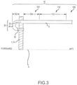
- Figure 3 depicts a side view of a circuit card 1 or a circuit card 9 having a conductor 3 inserted according to the teachings herein.
- a conductor 3 may comprise an at least partially insulated wire extending through a strain relief aperture of the circuit card 1 or circuit card 9 and electrically connected to a conductor contact of the circuit card 1 or circuit card 9.
- the conductor 3 may have a strain relief portion 31 and a conduction portion 32.
- the strain relief portion 31 may comprise a strain relief aperture pass-through 33 and a bent portion 34.
- the strain relief aperture pass-through 33 may comprise a portion of the conductor 3 inserted through a strain relief aperture.
- the bent portion 34 may comprise a radiused portion of the conductor 3 turning back toward the circuit card 1 or circuit card 9 after passage through the strain relief aperture, thereby positioning a conduction portion 32 of the conductor 3 into electrical contact with a conductor contact. In this manner, the conductor 3 may enjoy both electrical continuity with the conductor contact, and strain relief via the strain relief aperture.
- a circuit card 1 or circuit card 9 comprises one or more coating zone 10.
- a coating zone 10 may comprise a region extending axially (relative to a central axis 5) outward from the circuit card 1 or circuit card 9 and receiving a material coating.
- Various different material coatings may be applied, having various different thicknesses and material properties. The material coating is applied following the interfacing of a conductor 3 with the circuit card 1 or circuit card 9.
- the circuit card 1 or circuit card 9 comprising various coating zones 10 may be configured to interact in various ways with a conductor 3, surrounding structures such as a back shell, and/or the like.
- various coating zones 10 may receive a coating having various moisture barrier characteristics, dielectric constants, strengths, adhesive properties, and/or the like.
- a circuit card 1 or circuit card 9 comprise a conformal coating.
- the conformal coating has various regions.
- the conformal coating has a proximal coating zone 101 having a backside depth 104 and a front side depth 102, a mesial coating zone 110 having a mesial coating zone depth 112, and a distal coating zone 120.
- the proximal coating zone 101 comprises a conformal coating of a poly(p-xylylene) polymer, for example a halogenated parylene, a reactive parylene, or any desired parylene.
- the coating may comprise parylene N, or parylene C, or parylene X, or any parylene having properties as desired.
- the parylene is disposed on the aft (e.g., toward the direction of the conductor 3 and away from the plane of the circuit card 1) side of the circuit card 1 or circuit card 9 extending to a backside depth 104.
- the parylene is also disposed on the front (e.g., away from the direction of the conductor 3 and away from the plane of the circuit card) side of the circuit card 1 or circuit card 9 extending to a front side depth 102.
- the mesial coating zone 110 comprises a conformal coating of a poly(p-xylylene) polymer, for example a halogenated parylene, a reactive parylene, or any desired parylene.
- the coating may comprise parylene N, or parylene C, or parylene X, or any parylene having properties as desired.
- the parylene is axially outboard of the proximal coating zone 101 and on the aft (e.g., toward the direction of the conductor 3 and away from the plane of the circuit card) side of the circuit card 1 or circuit card 9.
- the mesial coating zone 110 extends to a mesial coating zone depth 112.
- a distal coating zone 120 comprises an area wherein conformal coating is prohibited.
- a distal coating zone 120 comprises a region axially outward of the mesial coating zone 110 and on the aft (e.g., toward the direction of the conductor 3 and away from the plane of the circuit card) side of the circuit card 1 or circuit card 9.
- the front side depth 102 may comprise a depth sufficient to overlay the bent portion 34 of a conductor 3.
- the front side depth 102 may comprise between about 0.115 inches (about 2.921 mm) to about 0.15 inches (about 3.81 mm).
- the backside depth 104 may comprise a depth sufficient to overlay a desired portion of the conductor 3, to achieve a desired property, for instance, adhesion of the conductor 3 to the circuit card 1 or circuit card 9 and/or a back shell, dielectric properties, and or the like.
- the backside depth 104 comprises about 0.25 inches (about 6.35 mm) to about 0.75 inches (about 19.05 mm). In various embodiments, the backside depth 104 comprises about 0.50 inches (about 12.7 mm).
- the mesial coating zone 110 may comprise a depth sufficient to overlay a desired portion of the conductor 3, to achieve a desired property, for instance, adhesion of the conductor 3 to the circuit card 1 or circuit card 9 and/or a back shell, dielectric properties, and/or the like.
- the mesial coating zone depth 112 comprises about 0.50 inches (about 12.7 mm) to about 1.0 inches (about 25.4 mm). In various embodiments, the mesial coating zone depth 112 comprises about 0.75 inches (about 19.05 mm).
- the conformal coating may be applied according to a desired thickness.
- conformal coating may be applied to proximal coating zone thickness within the proximal coating zone 101.
- the proximal coating zone thickness comprises a thickness of about .0005 (about 12.7 microns) inches to about .002 (about 50.8 microns) inches, or about .0005 (about 12.7 microns) inches to about .0007 (about 17.78 microns) inches or about .001 (about 25.4 microns) inches within the proximal coating zone 101, although any thickness as desired may be implemented.
- the conformal coating may be applied to a mesial coating zone thickness within the mesial coating zone 110.
- the conformal coating may be applied to a mesial coating zone thickness comprising about .0000 to about .0007 (about 17.78 microns) inches within the mesial coating zone 110.
- conformal coating may be prohibited to be applied in the distal coating zone 120.
- various layers of conformal coating may be applied to various thicknesses whereby various material properties are achieved.
- circuit card 1 or circuit card 9 is depicted in connection with a connector back shell 50, according to various embodiments.
- the combination of a circuit card 1 or circuit card 9 and a connector back shell 50 may comprise an electrical wiring system 100.
- a circuit card 1 or circuit card 9 may be disposed within the connector back shell 50 of a connector, whereby the signals, and/or power conducted via cabling connectorized at the connector back shell 50 of the connector may be conditioned. In this manner, electronic circuitry may be efficiently packaged with a connector back shell 50.
- the electrical wiring system 100 comprising a circuit card 1 or circuit card 9 and connector back shell 50 are field combinable.
- a circuit card 1 or circuit card 9 may be bondable to the connector back shell 50 by an adhesive.
- the circuit card 1 or circuit card 9 may be bondable to the connector back shell 50 by an adhesive directly joining between the conformal coating of the circuit card and the connector back shell 50. In this manner, the integrity of the conformal coating may be maintained. For instance, the bond may be accomplished without breaking of the conformal coating because the adhesive may bond directly between the conformally coated circuit card 1 or circuit card 9 and the connector back shell 50.
- two-sided tape and/or another desired adhesive may be disposed about the circumferentially outward edge of the circuit card 1 or circuit card 9 and/or along a portion of a face of the circuit card 1 or circuit card 9 (such as over a portion of a stay out zone 2 ( Figures 1-2 )) whereby the circuit card 1 or circuit card 9 may be press-fit against a portion of the connector back shell 50.
- the circuit card 1 or circuit card 9 is conformally coated prior to joining with the connector back shell 50.
- all or a portion of the electrical wiring system 100 is conformally coated after the circuit card 1 or circuit card 9 and the connector back shell 50 are joined.
Landscapes
- Engineering & Computer Science (AREA)
- Microelectronics & Electronic Packaging (AREA)
- Manufacturing & Machinery (AREA)
- Coupling Device And Connection With Printed Circuit (AREA)
- Credit Cards Or The Like (AREA)
- Structure Of Printed Boards (AREA)
Description
- The present disclosure relates to circuit cards, and more particularly, circuit cards for use within electrical connector assemblies.
- Aircraft typical include numerous sensor and effector systems whereby vehicle functions are controlled and monitored. Moreover, such systems typically include connectorized electrical wiring to conduct power and signals among different system components. However, in various instances, the strength of a signal conducted along connectorized electrical wiring degrades over the path of the wiring, such as due to parasitic shunt resistances. However, the installation of amplifiers along the path of connectorized electrical wiring contributes unwanted bulk and complexity to wiring systems, as well as increasing the number of connectors needed along a wiring path.
- According to various embodiments, a circuit card is provided as claimed in
claim 1. - In various embodiments, the mesial coating zone thickness and the proximal coating zone thickness are different.
- The circuit card may further include a bore including an opening disposed through the circuit card and positioned radially inward of the populated region. The bore may be located at a center of the circuit card. The bore may comprise a square aperture.
- The circuit card may include a labeling area including a crescent shaped partial annulus disposed within the populated region and radially opposite the first strain relief aperture.
- In various embodiments, the proximal coating zone thickness may be about .0005 to about .0007 inches (about 12.7 to 17.8 microns), and the mesial coating zone thickness may be about .0000 to about .0007 inches (about 0 to 17.8 microns). The backside depth may be about 0.05 inches (about 1.27 mm), and the front side depth may be between about .0015 inches to about .015 inches (about 38.1 to 381 microns). The mesial coating zone depth may be about 0.75 inches (about 19 mm).
- In various embodiments, the backside depth may be about 0.05 inches (1.27 mm), the front side depth may be between about .0015 inches to about .015 inches (about 38.1 to 381 microns), the mesial coating zone depth may be about 0.75 inches (about 19.1 mm), the proximal coating zone thickness may be about .0005 to about .002 inches (about 12.7 to 50.8 microns), or may be about .0005 to about .0007 inches (about 12.7 to 17.8 microns), or may be about .001 inches (25.4 microns), and the mesial coating zone thickness may be about .0000 to about .0007 inches (about 0 to 17.8 microns).
- According to various embodiments, an electrical wiring assembly is provided as claimed in
claim 10. - In various embodiments, the connector back shell is bonded directly to the circuit card by an adhesive disposed between the conformal coating of the circuit card and the connector back shell.
- A method of making a circuit card including a printed circuit board is provided as claimed in claim 11.
- The subject matter of the present disclosure is particularly pointed out and distinctly claimed in the concluding portion of the specification. A more complete understanding of the present disclosure, however, may best be obtained by referring to the detailed description and claims when considered in connection with the drawing figures, wherein like numerals denote like elements.
-
FIGs. 1 and2 depict end views of example circuit cards, in accordance with various embodiments; -
FIG. 3 depicts a side view of a circuit card, in accordance with various embodiments; and -
FIG. 4 depicts an electrical wiring system comprising a circuit card and a connector back shell, in accordance with various embodiments. - The present disclosure relates to a circuit card for electrical wiring systems. In various instances, signal degradation over the length of electrical wiring of an electrical wiring system gives rise to a desire to incorporate signal amplifiers in the electrical wiring. In various embodiments, various other electronics are desired to be implemented in the electrical wiring. In various embodiments, a circuit card is configured to be installed inside a back shell of a connector associated with the electrical wiring. In this manner, signal properties can be electronically manipulated, such as by being amplified, without need for bulky and obtrusive external amplifiers, or additional connectorization to insert an amplifier device in the path of the wiring. Thus, limited available space, such as the limited available space within an aircraft, is utilized efficiently, and without additional connectorization and/or potential failure points.
- For instance, with reference to
Figure 1 , according to various embodiments,circuit card 1 is disclosed. Acircuit card 1 comprises a printed circuit board (PCB). The printed circuit board may have a shape. In various embodiments, the shape of the printed circuit board corresponds to the shape of a volume within a connector back shell. For instance, in various embodiments, the printed circuit board is a round wafer, and is configured to fit within a connector back shell having a cylindrical portion. However, the printed circuit board may be trapezoidal, triangular, irregularly shaped, oval, and/or any shape as desired. - The
circuit card 1 comprises a variety of features. For instance, acircuit card 1 comprises a stay outzone 2. A stay outzone 2 comprises a region of the circuit card proximate to theboundary edge 7 of thecircuit card 1. The stay outzone 2 comprises a region of thecircuit card 1 coincident with a spark gap sufficiently small that in the event of overvoltage situations, such as a lightning strike, arcing would occur between uninsulated conductors (if any) in the stay outzone 2 and the surrounding connector back shell. Thus, the stay outzone 2 comprises a region of thecircuit card 1 wherein no uninsulated conductors are disposed. As such, conductors may be mated to thecircuit card 1 in different regions of thecircuit card 1, but may transition to being insulated if and when passing through the stay outzone 2. The stay outzone 2 comprises a strain relief aperture such as a first strain relief aperture 22-1, and may further comprise a second strain relief aperture 22-2, a third strain relief aperture 22-3, and/or any number of strain relief apertures 22-n. An insulated conductor passes through each strain relief aperture, whereby mechanical strain, such as tension, compression, torsion, side loads, and/or other mechanical loads, may be conducted along a load path away from an electrical connection between the conductor and thecircuit card 1, such as an electrical connection between a conductor and a conductor pad, such as conductor contact 42-1, 42-2, 42-3, and/or 42-n which would be positioned within other region(s) of thecircuit card 1. - The
circuit card 1 comprises aconductor interface region 4. Aconductor interface region 4 comprises a region of thecircuit card 1 proximate to the stay outzone 2, and radially inward of the stay outzone 2, such as adjoining the opposite side of the stay outzone 2 relative to theboundary edge 7. Theconductor interface region 4 is radially inward of the stay outzone 2 relative to acentral axis 5 of thecircuit card 1. In various embodiments, theconductor interface region 4 comprises a conductor contacts, such as a first conductor contact 42-1, and may further comprise a second conductor contact 42-2, a third conductor contact 42-3 and/or any number conductor contact 42-n. In various embodiments, there are an equal number of conductor contacts 42-1, 42-2, 42-3, 42-n as there are strain relief apertures 22-1, 22-2, 22-3, and 22-n. In this manner, eachconductor 3 interfacing with thecircuit card 1 at a conductor contact may also enjoy strain relief at a strain relief aperture. Each conductor contact is configured to receive a conductor in electrical communication with thecircuit card 1. For instance, a conductor contact may comprise a solder pad, or a through hole, or a lug, or a tab, or a flange, or a fastener, and/or any other mechanism whereby electrical continuity between a conductor and the conductor contact (and thus the circuit card 1) may be established. - The
circuit card 1 comprises a populatedregion 6. A populated region 6comprises a region of thecircuit card 1 that is populated or that is configured to be populated with electronic components, such as any number of active electronic components and/or passive electronic components. For instance, integrated circuits, resistors, capacitors, inductors, switches, semiconductor devices such as diodes and/or transistors, microprocessors, memories, amplifiers, and/or the like may populate the populatedregion 6. The populatedregion 6 comprises a region of thecircuit card 1 radially inward of theconductor interface region 4; however, the populatedregion 6 may also comprise any region of thecircuit card 1 as desired. In various embodiments, the populatedregion 6 comprises alabeling area 24. Alabeling area 24 may comprise a two dimensional surface area portion of the populatedregion 6 configured to have human-readable and/or machine readable graphics, text or other labeling applied. In various embodiments, thelabeling area 24 comprises a crescent shaped partial annulus disposed within the area of the populatedregion 6 and radially opposite the strain relief apertures 22-1, 22-2, 22-3, and/or 22-n. For instance, thelabeling area 24 may comprise a crescent shaped partial annulus disposed within the populatedregion 6 and radially opposite the first strain relief aperture 22-1. In various embodiments, thelabeling area 24 comprises a two dimensional surface area shaped as an annulus, partial annulus, or a trapezoid and/or any shape as desired. - The
circuit card 1 may comprise abore 8. Thebore 8 may comprise an opening disposed through thecircuit card 1 and positioned inwardly of thepopulated region 6. In various embodiments, thebore 8 is located at thecentral axis 5 of thecircuit card 1. Thebore 8 may be configured to permit other aspects of a connector extend through thecircuit card 1, for instance, connector pins, connector sockets, back shell components, and/or the like. Thebore 8 may have any desired shape. For instance, thebore 8 may be quadrilateral, trapezoidal or may be circular (seeFigure 2 ) or may be oval, or may be star shaped, or may be any shape as desired. Thebore 8 may comprise a square aperture. - With reference now to
Figure 2 ,circuit card 9, according to various embodiments, may share features of circuit card 1 (Figure 1 ), wherein like numerals denote like structures. Thecircuit card 9 comprises a circular printed circuit board comprising various features. For instance, thecircuit card 9 comprises a stay outzone 2 comprising a region of thecircuit card 9 proximate to theboundary edge 7 of thecircuit card 9 and having a first strain relief aperture 22-1, a second strain relief aperture 22-2, a third strain relief aperture 22-3, a fourth strain relief aperture 22-4, a fifth strain relief aperture 22-5, a sixth strain relief aperture 22-6, a seventh strain relief aperture 22-7 and an eighth strain relief aperture 22-8. Moreover, thecircuit card 9 comprises aconductor interface region 4 disposed radially inward of the stay outzone 2 and comprising a first conductor contact 42-1, a second conductor contact 42-2, a third conductor contact 42-2, a fourth conductor contact 42-4, a fifth conductor contact 42-5, a sixth conductor contact 42-6, a seventh conductor contact 42-7, and an eighth conductor contact 42-8. Thecircuit card 9 comprises apopulated region 6, comprising a region of thecircuit card 9 disposed radially inward of theconductor interface region 4 and populated with at least one of an active electronic component and/or a passive electronic component. Alabeling area 24 may comprise a crescent shaped partial annular section of thepopulated region 6 configured to receive labeling, such as by silk screen printing. Thecircuit card 9 may comprise abore 8, comprising a circular opening disposed through thecircuit card 9 and positioned at itscentral axis 5. - With reference to
Figure 3 , acircuit card more conductor 3, according to various embodiments. For instance, whileFigures 1 and2 depict end views of acircuit card 1 and acircuit card 9, respectively,Figure 3 depicts a side view of acircuit card 1 or acircuit card 9 having aconductor 3 inserted according to the teachings herein. Aconductor 3 may comprise an at least partially insulated wire extending through a strain relief aperture of thecircuit card 1 orcircuit card 9 and electrically connected to a conductor contact of thecircuit card 1 orcircuit card 9. For example, theconductor 3 may have astrain relief portion 31 and
aconduction portion 32. Thestrain relief portion 31 may comprise a strain relief aperture pass-through 33 and abent portion 34. The strain relief aperture pass-through 33 may comprise a portion of theconductor 3 inserted through a strain relief aperture. Thebent portion 34 may comprise a radiused portion of theconductor 3 turning back toward thecircuit card 1 orcircuit card 9 after passage through the strain relief aperture, thereby positioning aconduction portion 32 of theconductor 3 into electrical contact with a conductor contact. In this manner, theconductor 3 may enjoy both electrical continuity with the conductor contact, and strain relief via the strain relief aperture. - With ongoing reference to
Figure 3 , acircuit card 1 orcircuit card 9 comprises one ormore coating zone 10. Acoating zone 10 may comprise a region extending axially (relative to a central axis 5) outward from thecircuit card 1 orcircuit card 9 and receiving a material coating. Various different material coatings may be applied, having various different thicknesses and material properties. The material coating is applied following the interfacing of aconductor 3 with thecircuit card 1 orcircuit card 9. In this manner, thecircuit card 1 orcircuit card 9 comprisingvarious coating zones 10 may be configured to interact in various ways with aconductor 3, surrounding structures such as a back shell, and/or the like. For instance,various coating zones 10 may receive a coating having various moisture barrier characteristics, dielectric constants, strengths, adhesive properties, and/or the like. - A
circuit card 1 orcircuit card 9 comprise a conformal coating. The conformal coating has various regions. The conformal coating has aproximal coating zone 101 having abackside depth 104 and afront side depth 102, amesial coating zone 110 having a mesialcoating zone depth 112, and adistal coating zone 120. - The
proximal coating zone 101 comprises a conformal coating of a poly(p-xylylene) polymer, for example a halogenated parylene, a reactive parylene, or any desired parylene. For instance, the coating may comprise parylene N, or parylene C, or parylene X, or any parylene having properties as desired. The parylene is disposed on the aft (e.g., toward the direction of theconductor 3 and away from the plane of the circuit card 1) side of thecircuit card 1 orcircuit card 9 extending to abackside depth 104. Moreover, the parylene is also disposed on the front (e.g., away from the direction of theconductor 3 and away from the plane of the circuit card) side of thecircuit card 1 orcircuit card 9 extending to afront side depth 102. - Moreover, the
mesial coating zone 110 comprises a conformal coating of a poly(p-xylylene) polymer, for example a halogenated parylene, a reactive parylene, or any desired parylene. For instance, the coating may comprise parylene N, or parylene C, or parylene X, or any parylene having properties as desired. The parylene is axially outboard of theproximal coating zone 101 and on the aft (e.g., toward the direction of theconductor 3 and away from the plane of the circuit card) side of thecircuit card 1 orcircuit card 9. Themesial coating zone 110 extends to a mesialcoating zone depth 112. - Finally, a
distal coating zone 120 comprises an area wherein conformal coating is prohibited. Thus, adistal coating zone 120 comprises a region axially outward of themesial coating zone 110 and on the aft (e.g., toward the direction of theconductor 3 and away from the plane of the circuit card) side of thecircuit card 1 orcircuit card 9. - The
front side depth 102 may comprise a depth sufficient to overlay thebent portion 34 of aconductor 3. For instance, in various embodiments, thefront side depth 102 may comprise between about 0.115 inches (about 2.921 mm) to about 0.15 inches (about 3.81 mm). - The
backside depth 104 may comprise a depth sufficient to overlay a desired portion of theconductor 3, to achieve a desired property, for instance, adhesion of theconductor 3 to thecircuit card 1 orcircuit card 9 and/or a back shell, dielectric properties, and or the like. In various embodiments, thebackside depth 104 comprises about 0.25 inches (about 6.35 mm) to about 0.75 inches (about 19.05 mm). In various embodiments, thebackside depth 104 comprises about 0.50 inches (about 12.7 mm). - Finally, the
mesial coating zone 110 may comprise a depth sufficient to overlay a desired portion of theconductor 3, to achieve a desired property, for instance, adhesion of theconductor 3 to thecircuit card 1 orcircuit card 9 and/or a back shell, dielectric properties, and/or the like. In various embodiments, the mesialcoating zone depth 112 comprises about 0.50 inches (about 12.7 mm) to about 1.0 inches (about 25.4 mm). In various embodiments, the mesialcoating zone depth 112 comprises about 0.75 inches (about 19.05 mm). - In each coating zone wherein a conformal coating, such as of parylene, is applied, the conformal coating may be applied according to a desired thickness. For example, conformal coating may be applied to proximal coating zone thickness within the
proximal coating zone 101. In various embodiments, the proximal coating zone thickness comprises a thickness of about .0005 (about 12.7 microns) inches to about .002 (about 50.8 microns) inches, or about .0005 (about 12.7 microns) inches to about .0007 (about 17.78 microns) inches or about .001 (about 25.4 microns) inches within theproximal coating zone 101, although any thickness as desired may be implemented. - The conformal coating may be applied to a mesial coating zone thickness within the
mesial coating zone 110. For example, the conformal coating may be applied to a mesial coating zone thickness comprising about .0000 to about .0007 (about 17.78 microns) inches within themesial coating zone 110. As mentioned, conformal coating may be prohibited to be applied in thedistal coating zone 120. - Thus, various layers of conformal coating may be applied to various thicknesses whereby various material properties are achieved.
- With reference now to
Figure 4 , anexample circuit card 1 orcircuit card 9 is depicted in connection with a connector backshell 50, according to various embodiments. The combination of acircuit card 1 orcircuit card 9 and a connector backshell 50 may comprise anelectrical wiring system 100. As illustrated, acircuit card 1 orcircuit card 9 may be disposed within the connector backshell 50 of a connector, whereby the signals, and/or power conducted via cabling connectorized at the connector backshell 50 of the connector may be conditioned. In this manner, electronic circuitry may be efficiently packaged with a connector backshell 50. In various embodiments theelectrical wiring system 100 comprising acircuit card 1 orcircuit card 9 and connector backshell 50 are field combinable. For instance, acircuit card 1 orcircuit card 9 may be bondable to the connector backshell 50 by an adhesive. Thecircuit card 1 orcircuit card 9 may be bondable to the connector backshell 50 by an adhesive directly joining between the conformal coating of the circuit card and the connector backshell 50. In this manner, the integrity of the conformal coating may be maintained. For instance, the bond may be accomplished without breaking of the conformal coating because the adhesive may bond directly between the conformallycoated circuit card 1 orcircuit card 9 and the connector backshell 50. For instance, two-sided tape and/or another desired adhesive may be disposed about the circumferentially outward edge of thecircuit card 1 orcircuit card 9 and/or along a portion of a face of thecircuit card 1 or circuit card 9 (such as over a portion of a stay out zone 2 (Figures 1-2 )) whereby thecircuit card 1 orcircuit card 9 may be press-fit against a portion of the connector backshell 50. In various embodiments, thecircuit card 1 orcircuit card 9 is conformally coated prior to joining with the connector backshell 50. In further embodiments, all or a portion of theelectrical wiring system 100 is conformally coated after thecircuit card 1 orcircuit card 9 and the connector backshell 50 are joined.
Claims (11)
- A circuit card (1, 9) comprising a printed circuit board comprising:A first strain relief aperture (22-1 ... 22-8) positioned in and extending through a stay out zone (2) of the circuit card proximate to a boundary edge of the circuit card, the stay out zone comprising a region of the circuit card where no uninsulated conductors are disposed, wherein the stay out zone is coincident with a spark gap sufficiently small so as to avoid arcing in the event of overvoltage situations; anda first conductor contact (42-1... 42-8) positioned in a conductor interface region (4) of the circuit card (1, 9) proximate the stay out zone (2) and radially inward of the stay out zone relative to a central axis of the circuit card,wherein a populated region (6) of the circuit card (1, 9) configured to be populated with electronic components comprises a region of the circuit card (1, 9) radially inward of the conductor interface region (4); wherein a single conductor (3) is received through the first strain relief aperture (22-1) and connected in electrical communication with the first conductor contact, and a conformal coating of a poly(p-xylylene) polymer, the conformal coating having been applied following the interfacing of a conductor with the circuit card, and wherein the conformal coating comprises:a proximal coating zone (101) comprising a backside depth (104) on the aft side of the circuit card and a front side depth (102) on the front side of the circuit card, wherein the conformal coating comprises a proximal coating zone thickness;a distal coating zone (120) wherein conformal coating is prohibited; anda mesial coating zone (110) disposed between the proximal coating zone (101) and the distal coating zone (120) and comprising a mesial coating zone depth (112) wherein the conformal coating comprises a mesial coating zone thickness..
- The circuit card according to claim 1, further comprising a bore (8) comprising an opening disposed through the circuit card (1, 9) and positioned radially inward of the populated region (6).
- The circuit card according to claim 2, wherein the bore (8) is located at a center of the circuit card.
- The circuit card according to claim 3, wherein the bore (8) comprises a square aperture.
- The circuit card according to any preceding claim, further comprising a labeling area comprising a crescent shaped partial annulus disposed within the populated region and radially opposite the first strain relief aperture (22-1 ... 21-7).
- The circuit card according to any preceding claim, wherein the first conductor contact comprises at least one of a solder pad and a through hole.
- The circuit card according to claim 1, wherein the mesial coating zone thickness and the proximal coating zone thickness are different.
- The circuit card according to claim 1,wherein the proximal coating zone thickness comprises about 12.7 microns (.0005 inches) to about 50.8 microns (.002 inches), andwherein the mesial coating zone thickness comprises about 0 microns (.0000 inches) to about 17.78 microns (.0007 inches).
- The circuit card according to claim 1,wherein the backside depth (104) comprises about 1.27 mm (0.05 inches),wherein the front side depth (102) comprises between about 38 microns (.0015 inches) to about 380 microns (.015 inches), andwherein the mesial coating zone depth (112) comprises about 19.05 mm (0.75 inches), and optionallywherein the proximal coating zone thickness comprises about 13 microns (.0005 inches) to about 51 microns (.002 inches), andwherein the mesial coating zone thickness comprises about 0 to about 18 microns (.0000 to about .0007 inches).
- An electrical wiring assembly comprising:a connector back shell (50);the circuit card (1, 9) of any preceding claim disposed within the connector back shell (50), whereby at least one of signals and power conducted via a cable connectorized at the connector back shell (50) are conditioned,wherein the connector back shell (50) is bonded directly to the circuit card (1, 9) by an adhesive disposed between the conformal coating of the circuit card (1, 9) and the connector back shell (50).
- A method of making a circuit card (1, 9) comprising a printed circuit board comprising:forming a first strain relief aperture (22-1 ... 22-8) positioned in and extending through a stay out zone (2) of the circuit card proximate to a boundary edge of the circuit card (1, 9), the stay out zone comprising a region of the circuit card where no uninsulated conductors are disposed, wherein the stay out zone is coincident with a spark gap sufficiently small so as to avoid arcing in the event of overvoltage situations;forming a first conductor contact (42-1... 42-8) positioned in a conductor interface region (4) of the circuit card (1, 9) proximate the stay out zone (2) and radially inward of the stay out zone (2) relative to a central axis of the circuit card (1, 9),wherein a populated region (6) of the circuit card (1, 9) configured to be populated with electronic components comprises a region of the circuit card (1, 9) radially inward of the conductor interface region (4); wherein a single conductor (3) is received through the first strain relief aperture (22-1) and connected in electrical communication with the first conductor contact, and forming a conformal coating of a poly(p-xylylene) polymer over at least a portion of the circuit card, the conformal coating having been applied following the interfacing of a conductor with the circuit card, and wherein the conformal coating comprises:a proximal coating zone (101) comprising a backside depth (104) on the aft side of the circuit card and a front side depth (102) on the front side of the circuit card wherein the conformal coating comprises a proximal coating zone thickness;a distal coating zone (120) wherein conformal coating is prohibited; and
a mesial coating zone (110) disposed between the proximal coating zone (101) and the distal coating zone (120) and comprising a mesial coating zone depth (112) wherein the conformal coating comprises a mesial coating zone thickness.
Applications Claiming Priority (1)
| Application Number | Priority Date | Filing Date | Title |
|---|---|---|---|
| US14/817,886 US9728889B2 (en) | 2015-08-04 | 2015-08-04 | Circuit card |
Publications (3)
| Publication Number | Publication Date |
|---|---|
| EP3128820A2 EP3128820A2 (en) | 2017-02-08 |
| EP3128820A3 EP3128820A3 (en) | 2017-03-01 |
| EP3128820B1 true EP3128820B1 (en) | 2022-03-02 |
Family
ID=56802245
Family Applications (1)
| Application Number | Title | Priority Date | Filing Date |
|---|---|---|---|
| EP16182401.6A Active EP3128820B1 (en) | 2015-08-04 | 2016-08-02 | Circuit card |
Country Status (2)
| Country | Link |
|---|---|
| US (1) | US9728889B2 (en) |
| EP (1) | EP3128820B1 (en) |
Families Citing this family (1)
| Publication number | Priority date | Publication date | Assignee | Title |
|---|---|---|---|---|
| US9728889B2 (en) * | 2015-08-04 | 2017-08-08 | Goodrich Corporation | Circuit card |
Family Cites Families (26)
| Publication number | Priority date | Publication date | Assignee | Title |
|---|---|---|---|---|
| US4181394A (en) * | 1976-06-17 | 1980-01-01 | Pacific Electricord Company | Cord attachment plug |
| DE3137262C2 (en) * | 1981-09-18 | 1984-08-23 | Sds-Elektro Gmbh, 8024 Deisenhofen | Electrical connector for a cable containing a strain relief rope |
| USH113H (en) * | 1986-01-27 | 1986-08-05 | Waterblock and strain relief for electrical connectors | |
| US4734300A (en) * | 1986-03-14 | 1988-03-29 | Hughes Aircraft Company | Methods for removing parylene coatings from predetermined, desired areas of a substrate |
| US4720155A (en) * | 1986-04-04 | 1988-01-19 | Amphenol Corporation | Databus coupler electrical connector |
| US4900266A (en) * | 1989-03-08 | 1990-02-13 | Gsi Corporation | Strain relief system for connecting cables |
| US5044992A (en) * | 1989-10-20 | 1991-09-03 | The Charles Stark Draper Laboratory | Printed circuit injection molded connector with removable bifurcated contacts capable of high temperature exposure |
| US5244417A (en) | 1992-12-30 | 1993-09-14 | Perretta Frederick A | Backshell interface system |
| US5340333A (en) * | 1993-01-15 | 1994-08-23 | Interconnect Systems Group Inc. | Shielded modular adapter |
| US5342203A (en) * | 1993-05-25 | 1994-08-30 | United Technologies Corporation | Low profile backshell/wiring integration and interface system |
| US5655933A (en) * | 1995-05-04 | 1997-08-12 | Molex Incorporated | Power distribution system |
| JP3296731B2 (en) * | 1996-09-27 | 2002-07-02 | タイコエレクトロニクスアンプ株式会社 | Cable connector assembly and method of manufacturing the same |
| US6422885B2 (en) * | 1998-07-20 | 2002-07-23 | The Whitaker Corporation | Connector assembly adapted for axial realignment |
| US20040015630A1 (en) | 2002-07-19 | 2004-01-22 | Boolos Timothy L. | Connection system for connecting data transmitting and receiving devices to data transmission medium |
| US6821130B2 (en) * | 2002-08-16 | 2004-11-23 | Delphi Technologies, Inc. | Device and method using a flexible circuit secured for reliably inter-connecting components therein in the presence of vibration events |
| US7674117B2 (en) * | 2004-04-19 | 2010-03-09 | Michelin Recherche Et Technique S.A. | Strain-resistant electrical connection |
| US7479019B2 (en) * | 2004-07-23 | 2009-01-20 | Medconx, Inc. | Intelligent connector assembly for use in medical device cables |
| US7048564B1 (en) * | 2005-05-27 | 2006-05-23 | Delphi Technologies, Inc. | Sealed electronic module with fastenerless circuit board support post |
| US20070230142A1 (en) * | 2006-03-29 | 2007-10-04 | Engel John B | Zero parts strain relief |
| US7445490B2 (en) * | 2007-03-22 | 2008-11-04 | Deere & Company | Integrated overmolded cable seal and gasket for an electronic module |
| US7540773B2 (en) * | 2007-06-08 | 2009-06-02 | Hon Hai Precision Ind. Co., Ltd. | Connector assembly with improved strain relief structure |
| US8945307B2 (en) | 2009-12-23 | 2015-02-03 | Aeroquest Research Group Llc | Apparatus and method for vapor deposition of dielectric wire coating |
| US8292670B2 (en) | 2011-02-28 | 2012-10-23 | Honeywell International Inc. | Cable interface device |
| TWI472275B (en) * | 2013-02-18 | 2015-02-01 | King Shing Ind Co Ltd | An electric circuit board using metal plates and packaging module thereof |
| US9728889B2 (en) * | 2015-08-04 | 2017-08-08 | Goodrich Corporation | Circuit card |
| US9601866B1 (en) * | 2016-07-11 | 2017-03-21 | Elemental LED, Inc. | Strain relief and joint support |
-
2015
- 2015-08-04 US US14/817,886 patent/US9728889B2/en active Active
-
2016
- 2016-08-02 EP EP16182401.6A patent/EP3128820B1/en active Active
Also Published As
| Publication number | Publication date |
|---|---|
| EP3128820A2 (en) | 2017-02-08 |
| EP3128820A3 (en) | 2017-03-01 |
| US20170040739A1 (en) | 2017-02-09 |
| US9728889B2 (en) | 2017-08-08 |
Similar Documents
| Publication | Publication Date | Title |
|---|---|---|
| US9345140B2 (en) | Printed circuit board | |
| US9252510B2 (en) | Soldering structure for mounting connector on flexible circuit board | |
| US8202111B2 (en) | Connector and cable assembly | |
| US7245503B2 (en) | Circuit board having signal lines adapted to transmit high speed signals | |
| US9854679B2 (en) | Cable termination system | |
| EP4170712A3 (en) | Electronic assembly and electronic system with impedance matched interconnect structures | |
| EP0849793A2 (en) | Improvements in or relating to integrated circuit device packages | |
| US7666001B2 (en) | Circuit connection structure and printed circuit board | |
| US20130330944A1 (en) | Spring-loaded blind-mate electrical interconnect | |
| US10483182B2 (en) | Intermediate connector, semiconductor device including intermediate connector, and method of manufacturing intermediate connector | |
| US20200045815A1 (en) | Circuit board and electronic device including the same | |
| US9483673B2 (en) | Non-contact communication module and card reader | |
| CN110021829B (en) | Differential transmission cable module | |
| EP3128820A2 (en) | Circuit card | |
| US20170141490A1 (en) | Coaxial cable and connector with capacitive coupling | |
| US10076033B1 (en) | Printed circuit board with connector header mounted to bottom surface | |
| JP2020092081A5 (en) | Modules, electronics and imagers | |
| US7209361B2 (en) | Electronic device | |
| JP6311300B2 (en) | ESD protection device | |
| US20160192475A1 (en) | Wiring board | |
| JPH1126907A (en) | Printed wiring boards and electronic equipment | |
| JP2010118592A (en) | Semiconductor device | |
| US20200388969A1 (en) | Base board module | |
| KR102646368B1 (en) | Separable circuit board assembly and separable projectile including the same | |
| CN101790280B (en) | PCB (Printed circuit board), PCB assembly and electronic equipment |
Legal Events
| Date | Code | Title | Description |
|---|---|---|---|
| PUAI | Public reference made under article 153(3) epc to a published international application that has entered the european phase |
Free format text: ORIGINAL CODE: 0009012 |
|
| STAA | Information on the status of an ep patent application or granted ep patent |
Free format text: STATUS: THE APPLICATION HAS BEEN PUBLISHED |
|
| PUAL | Search report despatched |
Free format text: ORIGINAL CODE: 0009013 |
|
| AK | Designated contracting states |
Kind code of ref document: A2 Designated state(s): AL AT BE BG CH CY CZ DE DK EE ES FI FR GB GR HR HU IE IS IT LI LT LU LV MC MK MT NL NO PL PT RO RS SE SI SK SM TR |
|
| AX | Request for extension of the european patent |
Extension state: BA ME |
|
| AK | Designated contracting states |
Kind code of ref document: A3 Designated state(s): AL AT BE BG CH CY CZ DE DK EE ES FI FR GB GR HR HU IE IS IT LI LT LU LV MC MK MT NL NO PL PT RO RS SE SI SK SM TR |
|
| AX | Request for extension of the european patent |
Extension state: BA ME |
|
| RIC1 | Information provided on ipc code assigned before grant |
Ipc: H05K 1/02 20060101AFI20170126BHEP Ipc: H04L 12/40 20060101ALN20170126BHEP Ipc: H01R 13/66 20060101ALN20170126BHEP Ipc: H05K 1/11 20060101ALN20170126BHEP |
|
| STAA | Information on the status of an ep patent application or granted ep patent |
Free format text: STATUS: REQUEST FOR EXAMINATION WAS MADE |
|
| 17P | Request for examination filed |
Effective date: 20170831 |
|
| RBV | Designated contracting states (corrected) |
Designated state(s): AL AT BE BG CH CY CZ DE DK EE ES FI FR GB GR HR HU IE IS IT LI LT LU LV MC MK MT NL NO PL PT RO RS SE SI SK SM TR |
|
| STAA | Information on the status of an ep patent application or granted ep patent |
Free format text: STATUS: EXAMINATION IS IN PROGRESS |
|
| 17Q | First examination report despatched |
Effective date: 20200616 |
|
| GRAP | Despatch of communication of intention to grant a patent |
Free format text: ORIGINAL CODE: EPIDOSNIGR1 |
|
| STAA | Information on the status of an ep patent application or granted ep patent |
Free format text: STATUS: GRANT OF PATENT IS INTENDED |
|
| RIC1 | Information provided on ipc code assigned before grant |
Ipc: H04L 12/40 20060101ALN20210920BHEP Ipc: H01R 13/66 20060101ALN20210920BHEP Ipc: H05K 1/11 20060101ALN20210920BHEP Ipc: H05K 1/02 20060101AFI20210920BHEP |
|
| INTG | Intention to grant announced |
Effective date: 20211008 |
|
| GRAS | Grant fee paid |
Free format text: ORIGINAL CODE: EPIDOSNIGR3 |
|
| GRAA | (expected) grant |
Free format text: ORIGINAL CODE: 0009210 |
|
| STAA | Information on the status of an ep patent application or granted ep patent |
Free format text: STATUS: THE PATENT HAS BEEN GRANTED |
|
| AK | Designated contracting states |
Kind code of ref document: B1 Designated state(s): AL AT BE BG CH CY CZ DE DK EE ES FI FR GB GR HR HU IE IS IT LI LT LU LV MC MK MT NL NO PL PT RO RS SE SI SK SM TR |
|
| REG | Reference to a national code |
Ref country code: GB Ref legal event code: FG4D |
|
| REG | Reference to a national code |
Ref country code: CH Ref legal event code: EP Ref country code: AT Ref legal event code: REF Ref document number: 1473353 Country of ref document: AT Kind code of ref document: T Effective date: 20220315 |
|
| REG | Reference to a national code |
Ref country code: DE Ref legal event code: R096 Ref document number: 602016069524 Country of ref document: DE |
|
| REG | Reference to a national code |
Ref country code: IE Ref legal event code: FG4D |
|
| REG | Reference to a national code |
Ref country code: LT Ref legal event code: MG9D |
|
| REG | Reference to a national code |
Ref country code: NL Ref legal event code: MP Effective date: 20220302 |
|
| PG25 | Lapsed in a contracting state [announced via postgrant information from national office to epo] |
Ref country code: SE Free format text: LAPSE BECAUSE OF FAILURE TO SUBMIT A TRANSLATION OF THE DESCRIPTION OR TO PAY THE FEE WITHIN THE PRESCRIBED TIME-LIMIT Effective date: 20220302 Ref country code: RS Free format text: LAPSE BECAUSE OF FAILURE TO SUBMIT A TRANSLATION OF THE DESCRIPTION OR TO PAY THE FEE WITHIN THE PRESCRIBED TIME-LIMIT Effective date: 20220302 Ref country code: NO Free format text: LAPSE BECAUSE OF FAILURE TO SUBMIT A TRANSLATION OF THE DESCRIPTION OR TO PAY THE FEE WITHIN THE PRESCRIBED TIME-LIMIT Effective date: 20220602 Ref country code: LT Free format text: LAPSE BECAUSE OF FAILURE TO SUBMIT A TRANSLATION OF THE DESCRIPTION OR TO PAY THE FEE WITHIN THE PRESCRIBED TIME-LIMIT Effective date: 20220302 Ref country code: HR Free format text: LAPSE BECAUSE OF FAILURE TO SUBMIT A TRANSLATION OF THE DESCRIPTION OR TO PAY THE FEE WITHIN THE PRESCRIBED TIME-LIMIT Effective date: 20220302 Ref country code: ES Free format text: LAPSE BECAUSE OF FAILURE TO SUBMIT A TRANSLATION OF THE DESCRIPTION OR TO PAY THE FEE WITHIN THE PRESCRIBED TIME-LIMIT Effective date: 20220302 Ref country code: BG Free format text: LAPSE BECAUSE OF FAILURE TO SUBMIT A TRANSLATION OF THE DESCRIPTION OR TO PAY THE FEE WITHIN THE PRESCRIBED TIME-LIMIT Effective date: 20220602 |
|
| REG | Reference to a national code |
Ref country code: AT Ref legal event code: MK05 Ref document number: 1473353 Country of ref document: AT Kind code of ref document: T Effective date: 20220302 |
|
| PG25 | Lapsed in a contracting state [announced via postgrant information from national office to epo] |
Ref country code: PL Free format text: LAPSE BECAUSE OF FAILURE TO SUBMIT A TRANSLATION OF THE DESCRIPTION OR TO PAY THE FEE WITHIN THE PRESCRIBED TIME-LIMIT Effective date: 20220302 Ref country code: LV Free format text: LAPSE BECAUSE OF FAILURE TO SUBMIT A TRANSLATION OF THE DESCRIPTION OR TO PAY THE FEE WITHIN THE PRESCRIBED TIME-LIMIT Effective date: 20220302 Ref country code: GR Free format text: LAPSE BECAUSE OF FAILURE TO SUBMIT A TRANSLATION OF THE DESCRIPTION OR TO PAY THE FEE WITHIN THE PRESCRIBED TIME-LIMIT Effective date: 20220603 Ref country code: FI Free format text: LAPSE BECAUSE OF FAILURE TO SUBMIT A TRANSLATION OF THE DESCRIPTION OR TO PAY THE FEE WITHIN THE PRESCRIBED TIME-LIMIT Effective date: 20220302 |
|
| PG25 | Lapsed in a contracting state [announced via postgrant information from national office to epo] |
Ref country code: NL Free format text: LAPSE BECAUSE OF FAILURE TO SUBMIT A TRANSLATION OF THE DESCRIPTION OR TO PAY THE FEE WITHIN THE PRESCRIBED TIME-LIMIT Effective date: 20220302 |
|
| PG25 | Lapsed in a contracting state [announced via postgrant information from national office to epo] |
Ref country code: SM Free format text: LAPSE BECAUSE OF FAILURE TO SUBMIT A TRANSLATION OF THE DESCRIPTION OR TO PAY THE FEE WITHIN THE PRESCRIBED TIME-LIMIT Effective date: 20220302 Ref country code: SK Free format text: LAPSE BECAUSE OF FAILURE TO SUBMIT A TRANSLATION OF THE DESCRIPTION OR TO PAY THE FEE WITHIN THE PRESCRIBED TIME-LIMIT Effective date: 20220302 Ref country code: RO Free format text: LAPSE BECAUSE OF FAILURE TO SUBMIT A TRANSLATION OF THE DESCRIPTION OR TO PAY THE FEE WITHIN THE PRESCRIBED TIME-LIMIT Effective date: 20220302 Ref country code: PT Free format text: LAPSE BECAUSE OF FAILURE TO SUBMIT A TRANSLATION OF THE DESCRIPTION OR TO PAY THE FEE WITHIN THE PRESCRIBED TIME-LIMIT Effective date: 20220704 Ref country code: EE Free format text: LAPSE BECAUSE OF FAILURE TO SUBMIT A TRANSLATION OF THE DESCRIPTION OR TO PAY THE FEE WITHIN THE PRESCRIBED TIME-LIMIT Effective date: 20220302 Ref country code: CZ Free format text: LAPSE BECAUSE OF FAILURE TO SUBMIT A TRANSLATION OF THE DESCRIPTION OR TO PAY THE FEE WITHIN THE PRESCRIBED TIME-LIMIT Effective date: 20220302 Ref country code: AT Free format text: LAPSE BECAUSE OF FAILURE TO SUBMIT A TRANSLATION OF THE DESCRIPTION OR TO PAY THE FEE WITHIN THE PRESCRIBED TIME-LIMIT Effective date: 20220302 |
|
| PG25 | Lapsed in a contracting state [announced via postgrant information from national office to epo] |
Ref country code: IS Free format text: LAPSE BECAUSE OF FAILURE TO SUBMIT A TRANSLATION OF THE DESCRIPTION OR TO PAY THE FEE WITHIN THE PRESCRIBED TIME-LIMIT Effective date: 20220702 Ref country code: AL Free format text: LAPSE BECAUSE OF FAILURE TO SUBMIT A TRANSLATION OF THE DESCRIPTION OR TO PAY THE FEE WITHIN THE PRESCRIBED TIME-LIMIT Effective date: 20220302 |
|
| REG | Reference to a national code |
Ref country code: DE Ref legal event code: R097 Ref document number: 602016069524 Country of ref document: DE |
|
| PLBE | No opposition filed within time limit |
Free format text: ORIGINAL CODE: 0009261 |
|
| STAA | Information on the status of an ep patent application or granted ep patent |
Free format text: STATUS: NO OPPOSITION FILED WITHIN TIME LIMIT |
|
| PG25 | Lapsed in a contracting state [announced via postgrant information from national office to epo] |
Ref country code: DK Free format text: LAPSE BECAUSE OF FAILURE TO SUBMIT A TRANSLATION OF THE DESCRIPTION OR TO PAY THE FEE WITHIN THE PRESCRIBED TIME-LIMIT Effective date: 20220302 |
|
| 26N | No opposition filed |
Effective date: 20221205 |
|
| PG25 | Lapsed in a contracting state [announced via postgrant information from national office to epo] |
Ref country code: SI Free format text: LAPSE BECAUSE OF FAILURE TO SUBMIT A TRANSLATION OF THE DESCRIPTION OR TO PAY THE FEE WITHIN THE PRESCRIBED TIME-LIMIT Effective date: 20220302 |
|
| REG | Reference to a national code |
Ref country code: DE Ref legal event code: R119 Ref document number: 602016069524 Country of ref document: DE |
|
| PG25 | Lapsed in a contracting state [announced via postgrant information from national office to epo] |
Ref country code: MC Free format text: LAPSE BECAUSE OF FAILURE TO SUBMIT A TRANSLATION OF THE DESCRIPTION OR TO PAY THE FEE WITHIN THE PRESCRIBED TIME-LIMIT Effective date: 20220302 |
|
| REG | Reference to a national code |
Ref country code: CH Ref legal event code: PL |
|
| PG25 | Lapsed in a contracting state [announced via postgrant information from national office to epo] |
Ref country code: LU Free format text: LAPSE BECAUSE OF NON-PAYMENT OF DUE FEES Effective date: 20220802 Ref country code: LI Free format text: LAPSE BECAUSE OF NON-PAYMENT OF DUE FEES Effective date: 20220831 Ref country code: CH Free format text: LAPSE BECAUSE OF NON-PAYMENT OF DUE FEES Effective date: 20220831 |
|
| REG | Reference to a national code |
Ref country code: BE Ref legal event code: MM Effective date: 20220831 |
|
| P01 | Opt-out of the competence of the unified patent court (upc) registered |
Effective date: 20230522 |
|
| PG25 | Lapsed in a contracting state [announced via postgrant information from national office to epo] |
Ref country code: IT Free format text: LAPSE BECAUSE OF FAILURE TO SUBMIT A TRANSLATION OF THE DESCRIPTION OR TO PAY THE FEE WITHIN THE PRESCRIBED TIME-LIMIT Effective date: 20220302 Ref country code: IE Free format text: LAPSE BECAUSE OF NON-PAYMENT OF DUE FEES Effective date: 20220802 Ref country code: DE Free format text: LAPSE BECAUSE OF NON-PAYMENT OF DUE FEES Effective date: 20230301 |
|
| PG25 | Lapsed in a contracting state [announced via postgrant information from national office to epo] |
Ref country code: BE Free format text: LAPSE BECAUSE OF NON-PAYMENT OF DUE FEES Effective date: 20220831 |
|
| PG25 | Lapsed in a contracting state [announced via postgrant information from national office to epo] |
Ref country code: HU Free format text: LAPSE BECAUSE OF FAILURE TO SUBMIT A TRANSLATION OF THE DESCRIPTION OR TO PAY THE FEE WITHIN THE PRESCRIBED TIME-LIMIT; INVALID AB INITIO Effective date: 20160802 |
|
| PG25 | Lapsed in a contracting state [announced via postgrant information from national office to epo] |
Ref country code: MK Free format text: LAPSE BECAUSE OF FAILURE TO SUBMIT A TRANSLATION OF THE DESCRIPTION OR TO PAY THE FEE WITHIN THE PRESCRIBED TIME-LIMIT Effective date: 20220302 Ref country code: CY Free format text: LAPSE BECAUSE OF FAILURE TO SUBMIT A TRANSLATION OF THE DESCRIPTION OR TO PAY THE FEE WITHIN THE PRESCRIBED TIME-LIMIT Effective date: 20220302 |
|
| PG25 | Lapsed in a contracting state [announced via postgrant information from national office to epo] |
Ref country code: TR Free format text: LAPSE BECAUSE OF FAILURE TO SUBMIT A TRANSLATION OF THE DESCRIPTION OR TO PAY THE FEE WITHIN THE PRESCRIBED TIME-LIMIT Effective date: 20220302 |
|
| PG25 | Lapsed in a contracting state [announced via postgrant information from national office to epo] |
Ref country code: MT Free format text: LAPSE BECAUSE OF FAILURE TO SUBMIT A TRANSLATION OF THE DESCRIPTION OR TO PAY THE FEE WITHIN THE PRESCRIBED TIME-LIMIT Effective date: 20220302 |
|
| PGFP | Annual fee paid to national office [announced via postgrant information from national office to epo] |
Ref country code: GB Payment date: 20250724 Year of fee payment: 10 |
|
| PGFP | Annual fee paid to national office [announced via postgrant information from national office to epo] |
Ref country code: FR Payment date: 20250723 Year of fee payment: 10 |