EP3127202B1 - Vorrichtung zur leitung elektrischen gleichstroms - Google Patents
Vorrichtung zur leitung elektrischen gleichstroms Download PDFInfo
- Publication number
- EP3127202B1 EP3127202B1 EP15719465.5A EP15719465A EP3127202B1 EP 3127202 B1 EP3127202 B1 EP 3127202B1 EP 15719465 A EP15719465 A EP 15719465A EP 3127202 B1 EP3127202 B1 EP 3127202B1
- Authority
- EP
- European Patent Office
- Prior art keywords
- bus bar
- electrical
- busbars
- edge element
- direct current
- Prior art date
- Legal status (The legal status is an assumption and is not a legal conclusion. Google has not performed a legal analysis and makes no representation as to the accuracy of the status listed.)
- Active
Links
Images

Classifications
-
- H—ELECTRICITY
- H02—GENERATION; CONVERSION OR DISTRIBUTION OF ELECTRIC POWER
- H02G—INSTALLATION OF ELECTRIC CABLES OR LINES, OR OF COMBINED OPTICAL AND ELECTRIC CABLES OR LINES
- H02G5/00—Installations of bus-bars
- H02G5/02—Open installations
-
- H—ELECTRICITY
- H02—GENERATION; CONVERSION OR DISTRIBUTION OF ELECTRIC POWER
- H02G—INSTALLATION OF ELECTRIC CABLES OR LINES, OR OF COMBINED OPTICAL AND ELECTRIC CABLES OR LINES
- H02G5/00—Installations of bus-bars
-
- H—ELECTRICITY
- H01—ELECTRIC ELEMENTS
- H01B—CABLES; CONDUCTORS; INSULATORS; SELECTION OF MATERIALS FOR THEIR CONDUCTIVE, INSULATING OR DIELECTRIC PROPERTIES
- H01B1/00—Conductors or conductive bodies characterised by the conductive materials; Selection of materials as conductors
- H01B1/02—Conductors or conductive bodies characterised by the conductive materials; Selection of materials as conductors mainly consisting of metals or alloys
-
- H—ELECTRICITY
- H02—GENERATION; CONVERSION OR DISTRIBUTION OF ELECTRIC POWER
- H02G—INSTALLATION OF ELECTRIC CABLES OR LINES, OR OF COMBINED OPTICAL AND ELECTRIC CABLES OR LINES
- H02G5/00—Installations of bus-bars
- H02G5/005—Laminated bus-bars
Definitions
- the invention relates to a device for directing direct electrical current with at least one busbar.
- a busbar is understood here as an electrical conductor for the distribution of electrical energy.
- Busbars are usually made of copper or aluminum and electrically insulated.
- the document US 3829707 discloses a busbar having the features of the preamble of claim 1.
- the invention has for its object to provide an improved device for directing electrical DC with at least one busbar, which is particularly suitable for limiting electrical short-circuit currents.
- the object is achieved by the features of claim 1.
- Advantageous embodiments of the invention are the subject of the dependent claims.
- the edge elements serve to suppress high-frequency changing current components.
- the invention uses the skin effect in electrical conductors, are guided by the high-frequency changing electrical currents within a conductor primarily close to the outer surfaces of the conductor.
- high-frequency changing electrical currents are therefore conducted to the edge elements and suppressed there due to the lower than the busbars electrical conductivity of the edge elements.
- This effect advantageously makes it possible, in particular, to suppress portions of electrical short-circuit currents with high-frequency-changing current strengths which typically occur in DC circuit arrangements.
- the invention thus enables a simple and cost-effective reduction of electrical short-circuit currents in DC busbars.
- the invention provides at least two edge elements, which are arranged on opposite lateral outer surfaces of a busbar.
- the skin effect can be used even better and electrical short-circuit currents can advantageously be further reduced.
- a further embodiment of the invention provides a plurality of stacked juxtaposed busbars. This embodiment makes it possible to use not only the skin effect but also the proximity effect in order to displace high-frequency changing electrical currents into edge elements. Under the proximity effect is understood to mean a current displacement between two adjacent electrical conductors under the influence of alternating currents.
- At least one edge element preferably extends over a plurality of busbars arranged next to one another in a stack, wherein it is arranged on lateral outer surfaces of these busbars and is electrically conductively connected to these busbars.
- a further embodiment of the invention provides at least one busbar of copper or aluminum.
- a further embodiment of the invention provides at least one edge element made of iron or a steel, in particular of a stainless steel before.
- a further embodiment of the invention provides at least one strip or plate-shaped busbar.
- Strip or plate-shaped busbars advantageously allow good heat dissipation from the busbars.
- the invention provides for the use of a device according to the invention for limiting electrical short-circuit currents in an electrical circuit arrangement, wherein at least one busbar of the device is electrically connected to one pole of an electrical DC voltage source.
- This use advantageously utilizes the abovementioned reduction of electrical short-circuit currents of a device according to the invention.
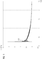
- FIG. 1 shows a typical course I (t) of a short-circuit current I in a DC circuit arrangement as a function of a time t.
- the current intensity of the short-circuit current I changes at high frequency by a time-decreasing mean value.
- the high-frequency changes of the short-circuit current I can be caused and influenced by various electrical components of a DC circuit arrangement, for example rectifiers or capacitors.
- FIG. 2 shows a cross-sectional view of a device 1 according to the invention for directing electrical DC.
- the device 1 comprises two busbars 3 and two edge elements 5.
- the two busbars 3 are similar and each strip-shaped running with a rectangular cross-sectional area and made for example of copper or aluminum.
- the two busbars 3 are arranged in a stack next to each other and parallel to each other and from each other.
- the two edge elements 5 are similar and each plate-like executed with a rectangular cross-sectional area and for example made of iron or a steel, in particular a stainless steel.
- Each edge element 5 rests against both busbars 3, wherein the edge elements 5 are arranged on mutually opposite sides of the busbars 3.
- each edge element 5 lies flat against a lateral outer surface 7 of each busbar 3 and is electrically conductively connected via these lateral outer surfaces 7 to both busbars 3.
- the two edge elements 5 each extend orthogonal to the plane of the drawing FIG. 2 over the entire length of the busbars 3.
- the edge elements 5, for example, by the busbars 3 about ten times further apart than the busbars 3 are spaced from each other.
- the thicknesses of the busbars 3 and the edge elements 5 correspond, for example, each about the distance of the busbars 3 from each other.
- the thicknesses of the busbars 3 and the edge elements 5 and the distance between the two busbars 3 from each other about 10 mm and the distance of the edge elements 5 from each other is about 100 mm.
- the length of one of the shorter sides of the rectangular contour of the cross-sectional area of the busbar 3 or of the edge element 5 is understood in each case as the thickness of a busbar 3 or an edge element 5.
- two in FIG. 2 used devices 1, wherein the busbars 3 of one of these devices 1 with a pole of a DC electrical power source and the busbars 3 of the other device 1 with the other pole of the DC electric power source are electrically connected.
Landscapes
- Emergency Protection Circuit Devices (AREA)
- Patch Boards (AREA)
- Non-Insulated Conductors (AREA)
- Installation Of Bus-Bars (AREA)
- Transformers For Measuring Instruments (AREA)
- Inverter Devices (AREA)
Description
- Die Erfindung betrifft eine Vorrichtung zur Leitung elektrischen Gleichstroms mit wenigstens einer Sammelschiene.
Unter einer Sammelschiene wird hier ein elektrischer Leiter zur Verteilung elektrischer Energie verstanden. Sammelschienen sind in der Regel aus Kupfer oder Aluminium gefertigt und elektrisch unisoliert ausgeführt. - Das Dokument
US 3829707 offenbart eine Sammelschiene mit den Merkmalen des Oberbegriffs des Anspruchs 1. Der Erfindung liegt die Aufgabe zugrunde, eine verbesserte Vorrichtung zur Leitung elektrischen Gleichstroms mit wenigstens einer Sammelschiene anzugeben, die insbesondere zur Begrenzung elektrischer Kurzschlussströme geeignet ist.
Die Aufgabe wird erfindungsgemäß durch die Merkmale des Anspruchs 1 gelöst.
Vorteilhafte Ausgestaltungen der Erfindung sind Gegenstand der Unteransprüche. - Die Randelemente dienen dabei der Unterdrückung von sich mit hohen Frequenzen ändernden Stromanteilen. Dazu nutzt die Erfindung den Skin-Effekt in elektrischen Leitern, durch den sich hochfrequent ändernde elektrische Ströme innerhalb eines Leiters vornehmlich nahe den Außenoberflächen des Leiters geführt werden. Durch die erfindungsgemäße Anordnung von Randelementen an Außenoberflächen von Sammelschienen werden sich hochfrequent ändernde elektrische Ströme daher zu den Randelementen geführt und dort aufgrund der gegenüber den Sammelschienen geringeren elektrischen Leitfähigkeit der Randelemente unterdrückt. Dieser Effekt ermöglicht vorteilhaft insbesondere die Unterdrückung von Anteilen elektrischer Kurzschlussströme mit sich hochfrequent ändernden Stromstärken, die typisch in Gleichstromschaltungsanordnungen auftreten. Die Erfindung ermöglicht dadurch eine einfache und kostengünstige Reduzierung elektrischer Kurzschlussströme in Gleichstromsammelschienen. Die Erfindung sieht wenigstens zwei Randelemente vor, die an sich gegenüber liegenden seitlichen Außenoberflächen einer Sammelschiene angeordnet sind.
Dadurch lässt sich der Skin-Effekt noch besser nutzen und elektrische Kurzschlussströme können vorteilhaft noch weiter reduziert werden.
Eine weitere Ausgestaltung der Erfindung sieht mehrere stapelartig nebeneinander angeordnete Sammelschienen vor.
Diese Ausgestaltung ermöglicht es, neben dem Skin-Effekt auch den Proximity-Effekt zu nutzen, um sich hochfrequent ändernde elektrische Ströme in Randelemente zu verdrängen. Unter dem Proximity-Effekt versteht man dabei eine Stromverdrängung zwischen zwei benachbarten elektrischen Leitern unter dem Einfluss von Wechselströmen.
Bei der vorgenannten Ausgestaltung der Erfindung erstreckt sich vorzugsweise wenigstens ein Randelement über mehrere stapelartig nebeneinander angeordnete Sammelschienen, wobei es an seitlichen Außenoberflächen dieser Sammelschienen angeordnet und mit diesen Sammelschienen jeweils elektrisch leitfähig verbunden ist. - Dies vereinfacht die Konstruktion der erfindungsgemäßen Vorrichtung, da ein Randelement für mehrere Sammelschienen genutzt werden kann und somit die einzelnen Sammelschienen nicht separat mit Randelementen versehen werden müssen.
- Eine weitere Ausgestaltung der Erfindung sieht wenigstens eine Sammelschiene aus Kupfer oder Aluminium vor.
- Kupfer und Aluminium eignen sich aufgrund ihrer hohen elektrischen Leitfähigkeit besonders gut als Materialien für Sammelschienen.
- Eine weitere Ausgestaltung der Erfindung sieht wenigstens ein Randelement aus Eisen oder einem Stahl, insbesondere aus einem nichtrostenden Stahl, vor.
- Eisen und Stahl, insbesondere nichtrostender Stahl, eignen sich aufgrund ihrer geringen elektrischen Leitfähigkeit besonders gut als Materialien für Randelemente.
- Eine weitere Ausgestaltung der Erfindung sieht wenigstens eine streifen- oder plattenförmig ausgebildete Sammelschiene vor.
- Streifen- oder plattenförmig ausgebildete Sammelschienen ermöglichen vorteilhaft eine gute Wärmeabfuhr aus den Sammelschienen.
- Die Erfindung sieht insbesondere die Verwendung einer erfindungsgemäßen Vorrichtung zur Begrenzung elektrischer Kurzschlussströme in einer elektrischen Schaltungsanordnung vor, wobei wenigstens eine Sammelschiene der Vorrichtung mit einem Pol einer elektrischen Gleichspannungsquelle elektrisch verbunden wird.
- Diese Verwendung nutzt vorteilhaft die oben genannte Reduzierung elektrischer Kurzschlussströme einer erfindungsgemäßen Vorrichtung.
- Die oben beschriebenen Eigenschaften, Merkmale und Vorteile dieser Erfindung sowie die Art und Weise, wie diese erreicht werden, werden klarer und deutlicher verständlich im Zusammenhang mit der folgenden Beschreibung von Ausführungsbeispielen, die im Zusammenhang mit den Zeichnungen näher erläutert werden. Dabei zeigen:
- FIG 1
- einen typischen Verlauf eines Kurzschlussstroms in einer Gleichstromschaltungsanordnung, und
- FIG 2
- eine Querschnittsdarstellung einer erfindungsgemäßen Vorrichtung zur Leitung elektrischen Gleichstroms.
-
Figur 1 zeigt einen typischen Verlauf I(t) eines Kurzschlussstroms I in einer Gleichstromschaltungsanordnung in Abhängigkeit von einer Zeit t. Die Stromstärke des Kurzschlussstroms I ändert sich hochfrequent um einen zeitlich abnehmenden Mittelwert. Die hochfrequenten Änderungen des Kurzschlussstroms I können dabei durch verschiedene elektrische Bauelemente einer Gleichstromschaltungsanordnung, beispielsweise von Gleichrichtern oder Kondensatoren, verursacht und beeinflusst werden. -
Figur 2 zeigt eine Querschnittsdarstellung einer erfindungsgemäßen Vorrichtung 1 zur Leitung elektrischen Gleichstroms. Die Vorrichtung 1 umfasst zwei Sammelschienen 3 und zwei Randelemente 5. - Die beiden Sammelschienen 3 sind gleichartig und jeweils streifenförmig mit einer rechteckigen Querschnittfläche ausgeführt und beispielsweise aus Kupfer oder Aluminium gefertigt. Die beiden Sammelschienen 3 sind stapelartig nebeneinander und parallel zueinander und voneinander beabstandet angeordnet.
- Die beiden Randelemente 5 sind gleichartig und jeweils plattenartig mit einer rechteckigen Querschnittfläche ausgeführt und beispielsweise aus Eisen oder einem Stahl, insbesondere einem nichtrostenden Stahl, gefertigt.
- Jedes Randelement 5 liegt an beiden Sammelschienen 3 an, wobei die Randelemente 5 an sich gegenüber liegenden Seiten der Sammelschienen 3 angeordnet sind. Dabei liegt jedes Randelement 5 flächig an einer seitlichen Außenoberfläche 7 jeder Sammelschiene 3 an und ist über diese seitlichen Außenoberflächen 7 mit beiden Sammelschienen 3 elektrisch leitend verbunden. Die beiden Randelemente 5 erstrecken sich jeweils orthogonal zur Zeichenebene der
Figur 2 über die gesamte Länge der Sammelschienen 3. - Die Randelemente 5 sind beispielsweise durch die Sammelschienen 3 etwa zehnmal weiter voneinander beabstandet als die Sammelschienen 3 voneinander beabstandet sind. Die Dicken der Sammelschienen 3 und der Randelemente 5 entsprechen beispielsweise jeweils etwa dem Abstand der Sammelschienen 3 voneinander. Beispielsweise betragen die Dicken der Sammelschienen 3 und der Randelemente 5 und der Abstand der beiden Sammelschienen 3 voneinander jeweils etwa 10 mm und der Abstand der Randelemente 5 voneinander beträgt etwa 100 mm. Dabei wird unter der Dicke einer Sammelschiene 3 bzw. eines Randelements 5 jeweils die Länge einer der kürzeren Seiten der rechteckigen Kontur der Querschnittsfläche der Sammelschiene 3 bzw. des Randelements 5 verstanden.
- In Gleichstromschaltungsanordnungen werden beispielsweise zwei in
Figur 2 dargestellte Vorrichtungen 1 verwendet, wobei die Sammelschienen 3 einer dieser Vorrichtungen 1 mit einem Pol einer elektrischen Gleichspannungsquelle und die Sammelschienen 3 der anderen Vorrichtung 1 mit dem anderen Pol der elektrischen Gleichspannungsquelle elektrisch verbunden werden. - Durch den Skin-Effekt und den Proximity-Effekt werden sich hochfrequent ändernde elektrische Ströme aus den Sammelschienen 3 in die Randelemente 5 geführt und durch den hohen elektrischen Widerstand der Randelemente 5 unterdrückt. Simulationen haben ergeben, dass dadurch der elektrische Widerstand einer in
Figur 2 dargestellten Vorrichtung 1 für sich hochfrequent ändernde elektrische Ströme um ein Vielfaches gegenüber dem elektrischen Widerstand der Sammelschienen 3 erhöht wird, beispielsweise um einen Faktor 39 für Stromänderungsfrequenzen von 1000 Hz bei Verwendung von Sammelschienen 3 aus Kupfer mit einer Querschnittsfläche von 2000 mm2 und Randelementen 5 aus Eisen. Bei einem Kurzschlussstrom I mit einer Pulshöhe von 220 kA führt dies zu einem Spannungsabfall von etwa 75 V/m entlang einer Vorrichtung 1. Bei Verwendung von nichtrostendem Stahl anstelle von Eisen als Material der Randelemente 5 können der elektrische Widerstand einer Vorrichtung 1 für hochfrequente Stromänderungen und der Spannungsabfall entlang der Vorrichtung 1 weiter erhöht werden. - Obwohl die Erfindung im Detail durch bevorzugte Ausführungsbeispiele näher illustriert und beschrieben wurde, so ist die Erfindung nicht durch die offenbarten Beispiele eingeschränkt und andere Variationen können vom Fachmann hieraus abgeleitet werden, ohne den Schutzumfang der Erfindung zu verlassen.
Claims (8)
- Vorrichtung (1) zur Leitung elektrischen Gleichstroms, umfassend wenigstens eine Sammelschiene (3) und wenigstens ein an einer seitlichen Außenoberfläche (7) der Sammelschiene (3) angeordnetes und sich entlang der Sammelschiene (3) erstreckendes elektrisch leitfähiges Randelement (5), das mit der Sammelschiene (3) elektrisch leitfähig verbunden ist und eine geringere elektrische Leitfähigkeit als die Sammelschiene (3) aufweist,
gekennzeichnet durch wenigstens zwei Randelemente (5), die an sich gegenüber liegenden seitlichen Außenoberflächen (7) einer Sammelschiene (3) angeordnet sind. - Vorrichtung (1) nach Anspruch 1,
gekennzeichnet durch mehrere stapelartig nebeneinander angeordnete Sammelschienen (3). - Vorrichtung (1) nach Anspruch 2,
gekennzeichnet durch wenigstens ein Randelement (5), das sich über mehrere stapelartig nebeneinander angeordnete Sammelschienen (3) erstreckt, wobei es an seitlichen Außenoberflächen (7) dieser Sammelschienen (3) angeordnet und mit diesen Sammelschienen (3) jeweils elektrisch leitfähig verbunden ist. - Vorrichtung (1) nach einem der vorhergehenden Ansprüche,
gekennzeichnet durch wenigstens eine Sammelschiene (3) aus Kupfer oder Aluminium. - Vorrichtung (1) nach einem der vorhergehenden Ansprüche,
gekennzeichnet durch wenigstens ein Randelement (5) aus Eisen oder einem Stahl. - Vorrichtung (1) nach einem der vorhergehenden Ansprüche,
gekennzeichnet durch wenigstens ein Randelement (5) aus einem nichtrostenden Stahl. - Vorrichtung (1) nach einem der vorhergehenden Ansprüche,
gekennzeichnet durch wenigstens eine streifen- oder plattenförmig ausgebildete Sammelschiene (3). - Verwendung einer Vorrichtung (1) nach einem der vorhergehenden Ansprüche zur Begrenzung elektrischer Kurzschlussströme (I) in einer elektrischen Schaltungsanordnung, wobei wenigstens eine Sammelschiene (3) der Vorrichtung (1) mit einem Pol einer elektrischen Gleichspannungsquelle elektrisch verbunden wird.
Applications Claiming Priority (2)
| Application Number | Priority Date | Filing Date | Title |
|---|---|---|---|
| EP14170388.4A EP2950407A1 (de) | 2014-05-28 | 2014-05-28 | Vorrichtung zur Leitung elektrischen Gleichstroms |
| PCT/EP2015/059040 WO2015180906A1 (de) | 2014-05-28 | 2015-04-27 | Vorrichtung zur leitung elektrischen gleichstroms |
Publications (2)
| Publication Number | Publication Date |
|---|---|
| EP3127202A1 EP3127202A1 (de) | 2017-02-08 |
| EP3127202B1 true EP3127202B1 (de) | 2018-02-28 |
Family
ID=50884249
Family Applications (2)
| Application Number | Title | Priority Date | Filing Date |
|---|---|---|---|
| EP14170388.4A Withdrawn EP2950407A1 (de) | 2014-05-28 | 2014-05-28 | Vorrichtung zur Leitung elektrischen Gleichstroms |
| EP15719465.5A Active EP3127202B1 (de) | 2014-05-28 | 2015-04-27 | Vorrichtung zur leitung elektrischen gleichstroms |
Family Applications Before (1)
| Application Number | Title | Priority Date | Filing Date |
|---|---|---|---|
| EP14170388.4A Withdrawn EP2950407A1 (de) | 2014-05-28 | 2014-05-28 | Vorrichtung zur Leitung elektrischen Gleichstroms |
Country Status (12)
| Country | Link |
|---|---|
| US (1) | US9882367B2 (de) |
| EP (2) | EP2950407A1 (de) |
| KR (1) | KR101935308B1 (de) |
| CN (1) | CN106415966B (de) |
| AU (1) | AU2015266301B2 (de) |
| BR (1) | BR112016027317B8 (de) |
| DK (1) | DK3127202T3 (de) |
| ES (1) | ES2671397T3 (de) |
| NO (1) | NO3127202T3 (de) |
| RU (1) | RU2656887C1 (de) |
| SG (1) | SG11201609198UA (de) |
| WO (1) | WO2015180906A1 (de) |
Families Citing this family (2)
| Publication number | Priority date | Publication date | Assignee | Title |
|---|---|---|---|---|
| US10340677B1 (en) * | 2016-12-14 | 2019-07-02 | NDI Engineering Company | Flexible electrical contact module |
| CN109873257A (zh) * | 2019-02-27 | 2019-06-11 | 国网陕西省电力公司电力科学研究院 | 降低接地装置冲击阻抗的电容补偿型接地体及制备方法 |
Family Cites Families (20)
| Publication number | Priority date | Publication date | Assignee | Title |
|---|---|---|---|---|
| US1561270A (en) * | 1920-09-17 | 1925-11-10 | Westinghouse Electric & Mfg Co | Bus bar |
| US1513340A (en) * | 1920-09-24 | 1924-10-28 | Westinghouse Electric & Mfg Co | Bus-bar structure |
| US1574993A (en) * | 1920-09-24 | 1926-03-02 | Westinghouse Electric & Mfg Co | Bus bar |
| US1582850A (en) * | 1920-09-24 | 1926-04-27 | Westinghouse Electric & Mfg Co | Bus-bar structure |
| FR1543660A (fr) * | 1967-11-02 | 1968-10-25 | Buna Chem Werke Veb | Ligne à courant fort pour le transport de courants continus de forte intensité |
| US3829707A (en) * | 1973-02-09 | 1974-08-13 | Allis Chalmers | Gas insulated high voltage electrical transmission line with means for damping transients |
| FR2233685B1 (de) * | 1973-06-12 | 1977-05-06 | Josse Bernard | |
| CH660817A5 (de) * | 1982-03-26 | 1987-06-15 | Bbc Brown Boveri & Cie | Anordnung zum schutz von gasisolierten, gekapselten schaltanlagen gegen hochfrequente spannungswanderwellen. |
| GB2160011A (en) * | 1984-06-05 | 1985-12-11 | Nat Res Dev | Electrical conductors |
| US4678253A (en) | 1984-10-29 | 1987-07-07 | Eaton Corporation | Bus duct having improved bus bar clamping structure |
| US5854445A (en) | 1996-08-06 | 1998-12-29 | General Electric Company | Thermally efficient power busway system with integral clamping mechanism |
| US6265666B1 (en) * | 1998-10-02 | 2001-07-24 | Siemens Energy & Automation, Inc. | Electrical power distribution busway having a two-piece housing |
| JP2008172976A (ja) | 2007-01-15 | 2008-07-24 | Toshiba Corp | 直流ガス絶縁母線 |
| DE102008049435A1 (de) * | 2008-09-25 | 2010-04-01 | Siemens Aktiengesellschaft | Sammelschienenanordnung mit einem ersten und zweiten Teilleiter |
| CN201297847Y (zh) * | 2008-11-17 | 2009-08-26 | 西安电炉研究所有限公司 | 一种节材汇流排 |
| JP2010246298A (ja) * | 2009-04-08 | 2010-10-28 | Sumitomo Electric Ind Ltd | バスバー,その形成方法およびバスバーモジュール |
| CN201466976U (zh) * | 2009-08-20 | 2010-05-12 | 石新春 | 一体化高频整流装置 |
| JP5738655B2 (ja) * | 2011-04-01 | 2015-06-24 | 株式会社東芝 | 密閉型開閉装置 |
| JP6088148B2 (ja) * | 2012-03-08 | 2017-03-01 | 三菱電線工業株式会社 | 集合導体及びその製造方法 |
| US9006571B2 (en) * | 2012-11-21 | 2015-04-14 | SAI Advanced Power Solutions | Bus system connecting bus bars and a method of connecting bus bars |
-
2014
- 2014-05-28 EP EP14170388.4A patent/EP2950407A1/de not_active Withdrawn
-
2015
- 2015-04-27 CN CN201580027746.4A patent/CN106415966B/zh active Active
- 2015-04-27 US US15/314,403 patent/US9882367B2/en not_active Expired - Fee Related
- 2015-04-27 RU RU2016145923A patent/RU2656887C1/ru active
- 2015-04-27 AU AU2015266301A patent/AU2015266301B2/en not_active Ceased
- 2015-04-27 DK DK15719465.5T patent/DK3127202T3/en active
- 2015-04-27 KR KR1020167033126A patent/KR101935308B1/ko not_active Expired - Fee Related
- 2015-04-27 ES ES15719465.5T patent/ES2671397T3/es active Active
- 2015-04-27 BR BR112016027317A patent/BR112016027317B8/pt not_active IP Right Cessation
- 2015-04-27 SG SG11201609198UA patent/SG11201609198UA/en unknown
- 2015-04-27 EP EP15719465.5A patent/EP3127202B1/de active Active
- 2015-04-27 WO PCT/EP2015/059040 patent/WO2015180906A1/de not_active Ceased
- 2015-04-27 NO NO15719465A patent/NO3127202T3/no unknown
Also Published As
| Publication number | Publication date |
|---|---|
| KR101935308B1 (ko) | 2019-01-04 |
| WO2015180906A1 (de) | 2015-12-03 |
| DK3127202T3 (en) | 2018-05-22 |
| AU2015266301A1 (en) | 2016-12-01 |
| CN106415966B (zh) | 2019-07-05 |
| SG11201609198UA (en) | 2016-12-29 |
| AU2015266301B2 (en) | 2018-11-01 |
| KR20160150636A (ko) | 2016-12-30 |
| ES2671397T3 (es) | 2018-06-06 |
| BR112016027317B1 (pt) | 2022-02-22 |
| BR112016027317B8 (pt) | 2023-04-25 |
| EP2950407A1 (de) | 2015-12-02 |
| RU2656887C1 (ru) | 2018-06-07 |
| EP3127202A1 (de) | 2017-02-08 |
| US9882367B2 (en) | 2018-01-30 |
| CN106415966A (zh) | 2017-02-15 |
| BR112016027317A8 (pt) | 2021-05-25 |
| BR112016027317A2 (pt) | 2017-08-15 |
| NO3127202T3 (de) | 2018-07-28 |
| US20170229854A1 (en) | 2017-08-10 |
Similar Documents
| Publication | Publication Date | Title |
|---|---|---|
| EP2659532B1 (de) | Batteriemodul mit verringerter gesamtinduktivität | |
| DE4110339A1 (de) | Wechselrichtereinheit mit verbesserter stromleiterplattenkonfiguration | |
| EP3446384B1 (de) | Antriebssystem mit einer zwischenkreisverschienung | |
| EP2302782A1 (de) | Stromrichteranordnung | |
| WO2010026038A1 (de) | Stromschiene und stromschienensystem in flachprofil-ausführung mit mehreren teilleiterschienen mit ausnehmungen an der schmalseite zum einrasten von kontaktfederelementen | |
| DE102015216771B4 (de) | Zwischenkreiskondensator für ein Mehrphasensystem | |
| DE102015223002A1 (de) | Leistungsumsetzungsvorrichtung und Eisenbahnfahrzeug mit derselben | |
| EP3332464B1 (de) | Vorrichtung zur herstellung einer mehrphasigen elektrischen verbindung sowie eine anordnung mit entsprechenden vorrichtungen | |
| DE102014114828A1 (de) | Anordnung mit einem Leistungshalbleitermodul, mit einer Gleichspannungsverschienung und mit einer Kondensatoreinrichtung | |
| DE112016006460B4 (de) | Leistungshalbleitermodul | |
| EP2950407A1 (de) | Vorrichtung zur Leitung elektrischen Gleichstroms | |
| EP2976832B1 (de) | Wechselrichter mit mindestens einer wechselrichterbrücke zwischen zwei busbars | |
| EP3392908B1 (de) | Leistungshalbleiteranordnung mit einem stapel von eine verbesserte geometrie aufweisenden anschlussplatten zur gemeinsamen elektrischen kontaktierungen mehrerer, gleichartiger leistungshalbleiter-schaltelemente | |
| DE102016102744B4 (de) | Leistungshalbleiteranordnung mit einer Mehrzahl von Leistungshalbleiter-Schaltelementen und verringerter Induktivitätsasymmetrie und Verwendung derselben | |
| EP3288046A1 (de) | Spulenvorrichtung | |
| DE102016209271A1 (de) | Verbindungsanordnung, insbesondere zur Verwendung in Elektrofahrzeugen oder Hybridfahrzeugen | |
| DE102015216083A1 (de) | Modulanordnung zum induktivitätsarmen Betrieb eines Leistungshalbleitermoduls an einem Gleichspannungskreis | |
| EP3799704B1 (de) | Leistungshalbleitermodul | |
| DE202009015987U1 (de) | Anschlussschrank als Verbindungseinrichtung zwischen PV-Modulen und mindestens einem Wechselrichter | |
| DE102017222114B4 (de) | AC Stromschiene für einen Wechselrichter | |
| DE102014201631B4 (de) | Anordnung zum Kontaktieren elektrischer Komponenten | |
| DE1465167A1 (de) | Anordnung mit mehreren Sammelschienen fuer elektrische Geraete | |
| DE202010008274U1 (de) | Elektrische Verbindung zwischen zwei Busbars aus ebenen Leitern und einer zwischen den Leitern angeordneten Isolationsschicht | |
| DE102019202728A1 (de) | Schaltungsanordnung zur Ansteuerung einer elektrischen Maschine | |
| DE898330C (de) | Elektrischer Kondensator bzw. Hochfrequenzspannungsteiler |
Legal Events
| Date | Code | Title | Description |
|---|---|---|---|
| PUAI | Public reference made under article 153(3) epc to a published international application that has entered the european phase |
Free format text: ORIGINAL CODE: 0009012 |
|
| 17P | Request for examination filed |
Effective date: 20161102 |
|
| AK | Designated contracting states |
Kind code of ref document: A1 Designated state(s): AL AT BE BG CH CY CZ DE DK EE ES FI FR GB GR HR HU IE IS IT LI LT LU LV MC MK MT NL NO PL PT RO RS SE SI SK SM TR |
|
| AX | Request for extension of the european patent |
Extension state: BA ME |
|
| RIN1 | Information on inventor provided before grant (corrected) |
Inventor name: TORGERSEN, HAAKON |
|
| RAP1 | Party data changed (applicant data changed or rights of an application transferred) |
Owner name: SIEMENS AKTIENGESELLSCHAFT |
|
| DAV | Request for validation of the european patent (deleted) | ||
| DAX | Request for extension of the european patent (deleted) | ||
| GRAP | Despatch of communication of intention to grant a patent |
Free format text: ORIGINAL CODE: EPIDOSNIGR1 |
|
| INTG | Intention to grant announced |
Effective date: 20170907 |
|
| GRAS | Grant fee paid |
Free format text: ORIGINAL CODE: EPIDOSNIGR3 |
|
| GRAA | (expected) grant |
Free format text: ORIGINAL CODE: 0009210 |
|
| AK | Designated contracting states |
Kind code of ref document: B1 Designated state(s): AL AT BE BG CH CY CZ DE DK EE ES FI FR GB GR HR HU IE IS IT LI LT LU LV MC MK MT NL NO PL PT RO RS SE SI SK SM TR |
|
| REG | Reference to a national code |
Ref country code: GB Ref legal event code: FG4D Free format text: NOT ENGLISH Ref country code: CH Ref legal event code: EP |
|
| REG | Reference to a national code |
Ref country code: AT Ref legal event code: REF Ref document number: 975125 Country of ref document: AT Kind code of ref document: T Effective date: 20180315 |
|
| REG | Reference to a national code |
Ref country code: IE Ref legal event code: FG4D Free format text: LANGUAGE OF EP DOCUMENT: GERMAN |
|
| REG | Reference to a national code |
Ref country code: DE Ref legal event code: R096 Ref document number: 502015003232 Country of ref document: DE |
|
| REG | Reference to a national code |
Ref country code: FR Ref legal event code: PLFP Year of fee payment: 4 |
|
| REG | Reference to a national code |
Ref country code: DK Ref legal event code: T3 Effective date: 20180517 Ref country code: SE Ref legal event code: TRGR |
|
| REG | Reference to a national code |
Ref country code: NL Ref legal event code: FP |
|
| REG | Reference to a national code |
Ref country code: ES Ref legal event code: FG2A Ref document number: 2671397 Country of ref document: ES Kind code of ref document: T3 Effective date: 20180606 |
|
| REG | Reference to a national code |
Ref country code: NO Ref legal event code: T2 Effective date: 20180228 |
|
| REG | Reference to a national code |
Ref country code: LT Ref legal event code: MG4D |
|
| PG25 | Lapsed in a contracting state [announced via postgrant information from national office to epo] |
Ref country code: CY Free format text: LAPSE BECAUSE OF FAILURE TO SUBMIT A TRANSLATION OF THE DESCRIPTION OR TO PAY THE FEE WITHIN THE PRESCRIBED TIME-LIMIT Effective date: 20180228 Ref country code: HR Free format text: LAPSE BECAUSE OF FAILURE TO SUBMIT A TRANSLATION OF THE DESCRIPTION OR TO PAY THE FEE WITHIN THE PRESCRIBED TIME-LIMIT Effective date: 20180228 Ref country code: LT Free format text: LAPSE BECAUSE OF FAILURE TO SUBMIT A TRANSLATION OF THE DESCRIPTION OR TO PAY THE FEE WITHIN THE PRESCRIBED TIME-LIMIT Effective date: 20180228 |
|
| PG25 | Lapsed in a contracting state [announced via postgrant information from national office to epo] |
Ref country code: GR Free format text: LAPSE BECAUSE OF FAILURE TO SUBMIT A TRANSLATION OF THE DESCRIPTION OR TO PAY THE FEE WITHIN THE PRESCRIBED TIME-LIMIT Effective date: 20180529 Ref country code: LV Free format text: LAPSE BECAUSE OF FAILURE TO SUBMIT A TRANSLATION OF THE DESCRIPTION OR TO PAY THE FEE WITHIN THE PRESCRIBED TIME-LIMIT Effective date: 20180228 Ref country code: BG Free format text: LAPSE BECAUSE OF FAILURE TO SUBMIT A TRANSLATION OF THE DESCRIPTION OR TO PAY THE FEE WITHIN THE PRESCRIBED TIME-LIMIT Effective date: 20180528 Ref country code: RS Free format text: LAPSE BECAUSE OF FAILURE TO SUBMIT A TRANSLATION OF THE DESCRIPTION OR TO PAY THE FEE WITHIN THE PRESCRIBED TIME-LIMIT Effective date: 20180228 |
|
| PG25 | Lapsed in a contracting state [announced via postgrant information from national office to epo] |
Ref country code: MT Free format text: LAPSE BECAUSE OF FAILURE TO SUBMIT A TRANSLATION OF THE DESCRIPTION OR TO PAY THE FEE WITHIN THE PRESCRIBED TIME-LIMIT Effective date: 20180228 |
|
| PG25 | Lapsed in a contracting state [announced via postgrant information from national office to epo] |
Ref country code: EE Free format text: LAPSE BECAUSE OF FAILURE TO SUBMIT A TRANSLATION OF THE DESCRIPTION OR TO PAY THE FEE WITHIN THE PRESCRIBED TIME-LIMIT Effective date: 20180228 Ref country code: RO Free format text: LAPSE BECAUSE OF FAILURE TO SUBMIT A TRANSLATION OF THE DESCRIPTION OR TO PAY THE FEE WITHIN THE PRESCRIBED TIME-LIMIT Effective date: 20180228 Ref country code: PL Free format text: LAPSE BECAUSE OF FAILURE TO SUBMIT A TRANSLATION OF THE DESCRIPTION OR TO PAY THE FEE WITHIN THE PRESCRIBED TIME-LIMIT Effective date: 20180228 Ref country code: AL Free format text: LAPSE BECAUSE OF FAILURE TO SUBMIT A TRANSLATION OF THE DESCRIPTION OR TO PAY THE FEE WITHIN THE PRESCRIBED TIME-LIMIT Effective date: 20180228 |
|
| REG | Reference to a national code |
Ref country code: DE Ref legal event code: R097 Ref document number: 502015003232 Country of ref document: DE |
|
| PG25 | Lapsed in a contracting state [announced via postgrant information from national office to epo] |
Ref country code: CZ Free format text: LAPSE BECAUSE OF FAILURE TO SUBMIT A TRANSLATION OF THE DESCRIPTION OR TO PAY THE FEE WITHIN THE PRESCRIBED TIME-LIMIT Effective date: 20180228 Ref country code: MC Free format text: LAPSE BECAUSE OF FAILURE TO SUBMIT A TRANSLATION OF THE DESCRIPTION OR TO PAY THE FEE WITHIN THE PRESCRIBED TIME-LIMIT Effective date: 20180228 Ref country code: SK Free format text: LAPSE BECAUSE OF FAILURE TO SUBMIT A TRANSLATION OF THE DESCRIPTION OR TO PAY THE FEE WITHIN THE PRESCRIBED TIME-LIMIT Effective date: 20180228 Ref country code: SM Free format text: LAPSE BECAUSE OF FAILURE TO SUBMIT A TRANSLATION OF THE DESCRIPTION OR TO PAY THE FEE WITHIN THE PRESCRIBED TIME-LIMIT Effective date: 20180228 |
|
| REG | Reference to a national code |
Ref country code: CH Ref legal event code: PL |
|
| REG | Reference to a national code |
Ref country code: BE Ref legal event code: MM Effective date: 20180430 |
|
| PLBE | No opposition filed within time limit |
Free format text: ORIGINAL CODE: 0009261 |
|
| STAA | Information on the status of an ep patent application or granted ep patent |
Free format text: STATUS: NO OPPOSITION FILED WITHIN TIME LIMIT |
|
| REG | Reference to a national code |
Ref country code: IE Ref legal event code: MM4A |
|
| PG25 | Lapsed in a contracting state [announced via postgrant information from national office to epo] |
Ref country code: LU Free format text: LAPSE BECAUSE OF NON-PAYMENT OF DUE FEES Effective date: 20180427 |
|
| 26N | No opposition filed |
Effective date: 20181129 |
|
| PG25 | Lapsed in a contracting state [announced via postgrant information from national office to epo] |
Ref country code: SI Free format text: LAPSE BECAUSE OF FAILURE TO SUBMIT A TRANSLATION OF THE DESCRIPTION OR TO PAY THE FEE WITHIN THE PRESCRIBED TIME-LIMIT Effective date: 20180228 Ref country code: BE Free format text: LAPSE BECAUSE OF NON-PAYMENT OF DUE FEES Effective date: 20180430 Ref country code: CH Free format text: LAPSE BECAUSE OF NON-PAYMENT OF DUE FEES Effective date: 20180430 Ref country code: LI Free format text: LAPSE BECAUSE OF NON-PAYMENT OF DUE FEES Effective date: 20180430 |
|
| PG25 | Lapsed in a contracting state [announced via postgrant information from national office to epo] |
Ref country code: IE Free format text: LAPSE BECAUSE OF NON-PAYMENT OF DUE FEES Effective date: 20180427 |
|
| GBPC | Gb: european patent ceased through non-payment of renewal fee |
Effective date: 20190427 |
|
| PG25 | Lapsed in a contracting state [announced via postgrant information from national office to epo] |
Ref country code: GB Free format text: LAPSE BECAUSE OF NON-PAYMENT OF DUE FEES Effective date: 20190427 |
|
| PG25 | Lapsed in a contracting state [announced via postgrant information from national office to epo] |
Ref country code: PT Free format text: LAPSE BECAUSE OF FAILURE TO SUBMIT A TRANSLATION OF THE DESCRIPTION OR TO PAY THE FEE WITHIN THE PRESCRIBED TIME-LIMIT Effective date: 20180228 |
|
| PG25 | Lapsed in a contracting state [announced via postgrant information from national office to epo] |
Ref country code: HU Free format text: LAPSE BECAUSE OF FAILURE TO SUBMIT A TRANSLATION OF THE DESCRIPTION OR TO PAY THE FEE WITHIN THE PRESCRIBED TIME-LIMIT; INVALID AB INITIO Effective date: 20150427 Ref country code: MK Free format text: LAPSE BECAUSE OF NON-PAYMENT OF DUE FEES Effective date: 20180228 |
|
| PG25 | Lapsed in a contracting state [announced via postgrant information from national office to epo] |
Ref country code: IS Free format text: LAPSE BECAUSE OF FAILURE TO SUBMIT A TRANSLATION OF THE DESCRIPTION OR TO PAY THE FEE WITHIN THE PRESCRIBED TIME-LIMIT Effective date: 20180628 |
|
| REG | Reference to a national code |
Ref country code: DE Ref legal event code: R081 Ref document number: 502015003232 Country of ref document: DE Owner name: SIEMENS ENERGY GLOBAL GMBH & CO. KG, DE Free format text: FORMER OWNER: SIEMENS AKTIENGESELLSCHAFT, 80333 MUENCHEN, DE |
|
| REG | Reference to a national code |
Ref country code: AT Ref legal event code: MM01 Ref document number: 975125 Country of ref document: AT Kind code of ref document: T Effective date: 20200427 |
|
| PG25 | Lapsed in a contracting state [announced via postgrant information from national office to epo] |
Ref country code: AT Free format text: LAPSE BECAUSE OF NON-PAYMENT OF DUE FEES Effective date: 20200427 |
|
| REG | Reference to a national code |
Ref country code: NO Ref legal event code: CHAD Owner name: SIEMENS ENERGY GLOBAL GMBH & CO. KG, DE |
|
| REG | Reference to a national code |
Ref country code: NL Ref legal event code: PD Owner name: SIEMENS ENERGY GLOBAL GMBH & CO. KG; DE Free format text: DETAILS ASSIGNMENT: CHANGE OF OWNER(S), ASSIGNMENT; FORMER OWNER NAME: SIEMENS AKTIENGESELLSCHAFT Effective date: 20221220 |
|
| REG | Reference to a national code |
Ref country code: FI Ref legal event code: PCE Owner name: SIEMENS ENERGY GLOBAL GMBH & CO. KG |
|
| PGFP | Annual fee paid to national office [announced via postgrant information from national office to epo] |
Ref country code: NL Payment date: 20230424 Year of fee payment: 9 |
|
| PGFP | Annual fee paid to national office [announced via postgrant information from national office to epo] |
Ref country code: NO Payment date: 20230419 Year of fee payment: 9 Ref country code: DK Payment date: 20230421 Year of fee payment: 9 |
|
| PGFP | Annual fee paid to national office [announced via postgrant information from national office to epo] |
Ref country code: TR Payment date: 20230407 Year of fee payment: 9 Ref country code: SE Payment date: 20230421 Year of fee payment: 9 |
|
| REG | Reference to a national code |
Ref country code: ES Ref legal event code: PC2A Owner name: SIEMENS ENERGY GLOBAL GMBH & CO. KG Effective date: 20240403 |
|
| REG | Reference to a national code |
Ref country code: DK Ref legal event code: EBP Effective date: 20240430 |
|
| REG | Reference to a national code |
Ref country code: SE Ref legal event code: EUG |
|
| REG | Reference to a national code |
Ref country code: NL Ref legal event code: MM Effective date: 20240501 |
|
| PG25 | Lapsed in a contracting state [announced via postgrant information from national office to epo] |
Ref country code: NO Free format text: LAPSE BECAUSE OF NON-PAYMENT OF DUE FEES Effective date: 20240430 |
|
| PG25 | Lapsed in a contracting state [announced via postgrant information from national office to epo] |
Ref country code: NL Free format text: LAPSE BECAUSE OF NON-PAYMENT OF DUE FEES Effective date: 20240501 |
|
| PG25 | Lapsed in a contracting state [announced via postgrant information from national office to epo] |
Ref country code: NO Free format text: LAPSE BECAUSE OF NON-PAYMENT OF DUE FEES Effective date: 20240430 Ref country code: NL Free format text: LAPSE BECAUSE OF NON-PAYMENT OF DUE FEES Effective date: 20240501 |
|
| PG25 | Lapsed in a contracting state [announced via postgrant information from national office to epo] |
Ref country code: DK Free format text: LAPSE BECAUSE OF NON-PAYMENT OF DUE FEES Effective date: 20240430 |
|
| PGFP | Annual fee paid to national office [announced via postgrant information from national office to epo] |
Ref country code: FI Payment date: 20250424 Year of fee payment: 11 |
|
| PGFP | Annual fee paid to national office [announced via postgrant information from national office to epo] |
Ref country code: DE Payment date: 20250428 Year of fee payment: 11 |
|
| PGFP | Annual fee paid to national office [announced via postgrant information from national office to epo] |
Ref country code: ES Payment date: 20250513 Year of fee payment: 11 |
|
| PGFP | Annual fee paid to national office [announced via postgrant information from national office to epo] |
Ref country code: IT Payment date: 20250422 Year of fee payment: 11 |
|
| PGFP | Annual fee paid to national office [announced via postgrant information from national office to epo] |
Ref country code: FR Payment date: 20250424 Year of fee payment: 11 |
|
| PG25 | Lapsed in a contracting state [announced via postgrant information from national office to epo] |
Ref country code: SE Free format text: LAPSE BECAUSE OF NON-PAYMENT OF DUE FEES Effective date: 20240428 |
|
| PG25 | Lapsed in a contracting state [announced via postgrant information from national office to epo] |
Ref country code: TR Free format text: LAPSE BECAUSE OF NON-PAYMENT OF DUE FEES Effective date: 20240427 |