EP3126293B1 - Oxydes et sulfures mixtes de bismuth et argent pour application photovoltaique - Google Patents
Oxydes et sulfures mixtes de bismuth et argent pour application photovoltaique Download PDFInfo
- Publication number
- EP3126293B1 EP3126293B1 EP15720356.3A EP15720356A EP3126293B1 EP 3126293 B1 EP3126293 B1 EP 3126293B1 EP 15720356 A EP15720356 A EP 15720356A EP 3126293 B1 EP3126293 B1 EP 3126293B1
- Authority
- EP
- European Patent Office
- Prior art keywords
- formula
- compound
- less
- type
- layer based
- Prior art date
- Legal status (The legal status is an assumption and is not a legal conclusion. Google has not performed a legal analysis and makes no representation as to the accuracy of the status listed.)
- Not-in-force
Links
Images

Classifications
-
- H—ELECTRICITY
- H10—SEMICONDUCTOR DEVICES; ELECTRIC SOLID-STATE DEVICES NOT OTHERWISE PROVIDED FOR
- H10F—INORGANIC SEMICONDUCTOR DEVICES SENSITIVE TO INFRARED RADIATION, LIGHT, ELECTROMAGNETIC RADIATION OF SHORTER WAVELENGTH OR CORPUSCULAR RADIATION
- H10F77/00—Constructional details of devices covered by this subclass
- H10F77/10—Semiconductor bodies
- H10F77/12—Active materials
-
- H—ELECTRICITY
- H10—SEMICONDUCTOR DEVICES; ELECTRIC SOLID-STATE DEVICES NOT OTHERWISE PROVIDED FOR
- H10F—INORGANIC SEMICONDUCTOR DEVICES SENSITIVE TO INFRARED RADIATION, LIGHT, ELECTROMAGNETIC RADIATION OF SHORTER WAVELENGTH OR CORPUSCULAR RADIATION
- H10F99/00—Subject matter not provided for in other groups of this subclass
-
- C—CHEMISTRY; METALLURGY
- C01—INORGANIC CHEMISTRY
- C01G—COMPOUNDS CONTAINING METALS NOT COVERED BY SUBCLASSES C01D OR C01F
- C01G29/00—Compounds of bismuth
- C01G29/006—Compounds containing bismuth, with or without oxygen or hydrogen, and containing two or more other elements
-
- H—ELECTRICITY
- H01—ELECTRIC ELEMENTS
- H01G—CAPACITORS; CAPACITORS, RECTIFIERS, DETECTORS, SWITCHING DEVICES, LIGHT-SENSITIVE OR TEMPERATURE-SENSITIVE DEVICES OF THE ELECTROLYTIC TYPE
- H01G9/00—Electrolytic capacitors, rectifiers, detectors, switching devices, light-sensitive or temperature-sensitive devices; Processes of their manufacture
- H01G9/20—Light-sensitive devices
- H01G9/2027—Light-sensitive devices comprising an oxide semiconductor electrode
- H01G9/2031—Light-sensitive devices comprising an oxide semiconductor electrode comprising titanium oxide, e.g. TiO2
-
- H—ELECTRICITY
- H10—SEMICONDUCTOR DEVICES; ELECTRIC SOLID-STATE DEVICES NOT OTHERWISE PROVIDED FOR
- H10F—INORGANIC SEMICONDUCTOR DEVICES SENSITIVE TO INFRARED RADIATION, LIGHT, ELECTROMAGNETIC RADIATION OF SHORTER WAVELENGTH OR CORPUSCULAR RADIATION
- H10F10/00—Individual photovoltaic cells, e.g. solar cells
- H10F10/10—Individual photovoltaic cells, e.g. solar cells having potential barriers
- H10F10/16—Photovoltaic cells having only PN heterojunction potential barriers
-
- H—ELECTRICITY
- H10—SEMICONDUCTOR DEVICES; ELECTRIC SOLID-STATE DEVICES NOT OTHERWISE PROVIDED FOR
- H10F—INORGANIC SEMICONDUCTOR DEVICES SENSITIVE TO INFRARED RADIATION, LIGHT, ELECTROMAGNETIC RADIATION OF SHORTER WAVELENGTH OR CORPUSCULAR RADIATION
- H10F71/00—Manufacture or treatment of devices covered by this subclass
-
- H—ELECTRICITY
- H10—SEMICONDUCTOR DEVICES; ELECTRIC SOLID-STATE DEVICES NOT OTHERWISE PROVIDED FOR
- H10K—ORGANIC ELECTRIC SOLID-STATE DEVICES
- H10K30/00—Organic devices sensitive to infrared radiation, light, electromagnetic radiation of shorter wavelength or corpuscular radiation
- H10K30/10—Organic devices sensitive to infrared radiation, light, electromagnetic radiation of shorter wavelength or corpuscular radiation comprising heterojunctions between organic semiconductors and inorganic semiconductors
- H10K30/15—Sensitised wide-bandgap semiconductor devices, e.g. dye-sensitised TiO2
- H10K30/151—Sensitised wide-bandgap semiconductor devices, e.g. dye-sensitised TiO2 the wide bandgap semiconductor comprising titanium oxide, e.g. TiO2
-
- H—ELECTRICITY
- H10—SEMICONDUCTOR DEVICES; ELECTRIC SOLID-STATE DEVICES NOT OTHERWISE PROVIDED FOR
- H10K—ORGANIC ELECTRIC SOLID-STATE DEVICES
- H10K30/00—Organic devices sensitive to infrared radiation, light, electromagnetic radiation of shorter wavelength or corpuscular radiation
- H10K30/10—Organic devices sensitive to infrared radiation, light, electromagnetic radiation of shorter wavelength or corpuscular radiation comprising heterojunctions between organic semiconductors and inorganic semiconductors
- H10K30/15—Sensitised wide-bandgap semiconductor devices, e.g. dye-sensitised TiO2
- H10K30/152—Sensitised wide-bandgap semiconductor devices, e.g. dye-sensitised TiO2 the wide bandgap semiconductor comprising zinc oxide, e.g. ZnO
-
- H—ELECTRICITY
- H10—SEMICONDUCTOR DEVICES; ELECTRIC SOLID-STATE DEVICES NOT OTHERWISE PROVIDED FOR
- H10K—ORGANIC ELECTRIC SOLID-STATE DEVICES
- H10K85/00—Organic materials used in the body or electrodes of devices covered by this subclass
- H10K85/10—Organic polymers or oligomers
- H10K85/111—Organic polymers or oligomers comprising aromatic, heteroaromatic, or aryl chains, e.g. polyaniline, polyphenylene or polyphenylene vinylene
-
- H—ELECTRICITY
- H10—SEMICONDUCTOR DEVICES; ELECTRIC SOLID-STATE DEVICES NOT OTHERWISE PROVIDED FOR
- H10K—ORGANIC ELECTRIC SOLID-STATE DEVICES
- H10K85/00—Organic materials used in the body or electrodes of devices covered by this subclass
- H10K85/10—Organic polymers or oligomers
- H10K85/111—Organic polymers or oligomers comprising aromatic, heteroaromatic, or aryl chains, e.g. polyaniline, polyphenylene or polyphenylene vinylene
- H10K85/113—Heteroaromatic compounds comprising sulfur or selene, e.g. polythiophene
- H10K85/1135—Polyethylene dioxythiophene [PEDOT]; Derivatives thereof
-
- C—CHEMISTRY; METALLURGY
- C01—INORGANIC CHEMISTRY
- C01P—INDEXING SCHEME RELATING TO STRUCTURAL AND PHYSICAL ASPECTS OF SOLID INORGANIC COMPOUNDS
- C01P2004/00—Particle morphology
- C01P2004/50—Agglomerated particles
-
- C—CHEMISTRY; METALLURGY
- C01—INORGANIC CHEMISTRY
- C01P—INDEXING SCHEME RELATING TO STRUCTURAL AND PHYSICAL ASPECTS OF SOLID INORGANIC COMPOUNDS
- C01P2004/00—Particle morphology
- C01P2004/60—Particles characterised by their size
- C01P2004/61—Micrometer sized, i.e. from 1-100 micrometer
-
- C—CHEMISTRY; METALLURGY
- C01—INORGANIC CHEMISTRY
- C01P—INDEXING SCHEME RELATING TO STRUCTURAL AND PHYSICAL ASPECTS OF SOLID INORGANIC COMPOUNDS
- C01P2004/00—Particle morphology
- C01P2004/60—Particles characterised by their size
- C01P2004/62—Submicrometer sized, i.e. from 0.1-1 micrometer
-
- C—CHEMISTRY; METALLURGY
- C01—INORGANIC CHEMISTRY
- C01P—INDEXING SCHEME RELATING TO STRUCTURAL AND PHYSICAL ASPECTS OF SOLID INORGANIC COMPOUNDS
- C01P2006/00—Physical properties of inorganic compounds
- C01P2006/40—Electric properties
-
- Y—GENERAL TAGGING OF NEW TECHNOLOGICAL DEVELOPMENTS; GENERAL TAGGING OF CROSS-SECTIONAL TECHNOLOGIES SPANNING OVER SEVERAL SECTIONS OF THE IPC; TECHNICAL SUBJECTS COVERED BY FORMER USPC CROSS-REFERENCE ART COLLECTIONS [XRACs] AND DIGESTS
- Y02—TECHNOLOGIES OR APPLICATIONS FOR MITIGATION OR ADAPTATION AGAINST CLIMATE CHANGE
- Y02E—REDUCTION OF GREENHOUSE GAS [GHG] EMISSIONS, RELATED TO ENERGY GENERATION, TRANSMISSION OR DISTRIBUTION
- Y02E10/00—Energy generation through renewable energy sources
- Y02E10/50—Photovoltaic [PV] energy
-
- Y—GENERAL TAGGING OF NEW TECHNOLOGICAL DEVELOPMENTS; GENERAL TAGGING OF CROSS-SECTIONAL TECHNOLOGIES SPANNING OVER SEVERAL SECTIONS OF THE IPC; TECHNICAL SUBJECTS COVERED BY FORMER USPC CROSS-REFERENCE ART COLLECTIONS [XRACs] AND DIGESTS
- Y02—TECHNOLOGIES OR APPLICATIONS FOR MITIGATION OR ADAPTATION AGAINST CLIMATE CHANGE
- Y02E—REDUCTION OF GREENHOUSE GAS [GHG] EMISSIONS, RELATED TO ENERGY GENERATION, TRANSMISSION OR DISTRIBUTION
- Y02E10/00—Energy generation through renewable energy sources
- Y02E10/50—Photovoltaic [PV] energy
- Y02E10/549—Organic PV cells
Definitions
- the present invention relates to the field of inorganic semiconductor compounds, in particular intended to provide a photocurrent, in particular by photovoltaic effect.
- photovoltaic technologies using inorganic compounds are mainly based on silicon technologies (over 80% of the market) and on thin film technologies (mainly CdTe and CIGS (Copper Indium Gallium Selenium), representing 20% of the market).
- CdTe and CIGS Copper Indium Gallium Selenium
- CZTS Cu 2 ZnSnSe 4
- An object of the present invention is precisely to provide inorganic compounds alternative to those used in current photovoltaic technologies, which make it possible to avoid the aforementioned problems.
- the present invention proposes to use a new family of inorganic materials, whose inventors have now shown that, unexpectedly, they prove to have good efficiency, and that they have the advantage of not having to use, or at a very low level, rare or toxic metals of the type In, Te, Cd mentioned above, and furthermore offer the possibility of using anions, such as Se or Te, in a reduced content, even not to use this type of anions.
- the elements M, M 'and M are generally substitution elements respectively occupying the place of the element Bi, the element Ag and the element S.
- material comprising at least one compound of formula (I) is meant a solid, generally in divided form (powder, dispersion) or in the form of a coating or a continuous or discontinuous layer on a support, and which comprises, or even consists of, a compound of formula (I).
- Ring earth means the elements of the group constituted by yttrium and scandium and the elements of the periodic classification of atomic number inclusive between 57 and 71.
- the compound of formula (I) according to the invention has the following formula: BiAg 1- ⁇ OS.
- At least one of the numbers x, y or z is non-zero.
- the element M may preferably be chosen from the elements Sb, Pb, Ba and the rare earth elements.
- the element M may for example be lutetium.
- the element M ' may preferably be selected from the elements Cu, Zn, Mn.
- the element M ' may for example be the element Cu.
- the element M can in particular be the element I.
- the compound of formula (I) according to the invention corresponds to the following formula: Bi 1-x M x Ag 1 - ⁇ OS (I a ), where x ⁇ 0, ⁇ is a zero or non-zero number and M is an element or a mixture of elements selected from the group (A) consisting of Pb, Sn, Hg, Ca, Sr, Ba, Sb, In, Ti, Mg , rare earths.
- M is an element or a mixture of elements chosen from rare earths.
- the compound of formula (I) according to the invention corresponds to the following formula: BiAg 1-y- ⁇ M ' y OS (I b ), where y ⁇ 0, ⁇ is a number no or non-zero and M 'is a member or a mixture of elements selected from the group (B) consisting of Ti, V, Cr, Mn, Fe, Co, Ni, Cu, Zn, Ga, Al, Cd, Pt, Pd.
- M ' is an element or a mixture of elements chosen from Cu and Zn elements.
- the compound of formula (I) according to the invention corresponds to the following formula: M z BiAgOS "1-z (I c), where z ⁇ 0, ⁇ is a non-zero number or null and M "is a halogen.
- the subject of the invention is also a method for preparing the material according to the invention comprising a step of solid grinding of a mixture comprising at least inorganic compounds of bismuth and of silver, and optionally at least one oxide, sulfide, oxysulfide, halide or oxyhalide of at least one element selected from Bi and the elements of group (A) consisting of Pb, Sn, Hg, Ca, Sr, Ba, Sb, In, Ti, Mg, rare earths, and optionally at least one oxide, sulfide, oxysulfide, halide or oxyhalide of at least one element selected from Ag and the elements of group (B) consisting of Ti, V, Cr, Mn, Fe, Co, Ni, Cu, Zn, Ga, Al, Cd, Pt, Pd.
- a solid form mixture comprising at least inorganic bismuth and silver compounds is ground.
- the inorganic compounds of bismuth and of silver present in the mixture are at least the compounds Bi 2 O 3 , Bi 2 S 3 and Ag 2 S.
- This grinding can be done according to any known means.
- This mixture can in particular be placed in an agate mortar.
- the grinding may for example be carried out with a planetary mill.
- grinding balls which consist for example of stainless steel balls, special chromium steel balls, agate balls, tungsten carbide balls , balls made of zirconium oxide.
- the grinding time can be adjusted according to the desired product. he can in particular be between 20 minutes and 96 hours, especially between 1 hour and 72 hours.
- Inorganic compounds of bismuth and silver in the mixture may be in the form of particles having a particle size less than 50 microns, in particular less than 10 microns, for example less than 1 micron.
- the particle sizes referred to herein can typically be measured by scanning electron microscopy (SEM).
- the compound that is present in the semiconductor material is a substituted inorganic material, in particular of the p type.
- substitutions such as the substitution of the element Bi by rare earths or by the element Sb or even the substitution of the element Ag by the Cu element
- these substitutions can, in particular by modifying the mesh parameters and / or by modifying the extension of the orbitals and their energy position, thus causing changes in the gap (valence band - conduction band).
- the aliovalent substitutions modify the degree of oxidation of the Ag element.
- the introduction of substituents in the structure of the semiconductor may, as the case may be, cause a reduction or an increase in the number of charge carriers.
- the substituted materials may in particular have a higher conductivity, which induces an improved conduction capacity, compared to its unsubstituted form, or conversely a lower conductivity.
- the inventors have now demonstrated that the materials corresponding to the above formula (I), in particular, when they are p-type, are capable of providing a photocurrent when they are irradiated under a wavelength greater than their gap (namely the generation of an electron-hole pair within the material under the effect of an incident photon of sufficient energy, the charged species formed (the electron and the hole ", namely the electron gap) being free to move to generate a current).
- the inventors have now demonstrated that the materials of the invention prove to be suitable for ensuring a photovoltaic effect.
- the photovoltaic effect is typically obtained by placing a material based on a semiconductor of formula (I) above, which is also specifically of the p type, in contact with a semiconductor n-type between two electrodes, in direct contact or optionally connected to at least one of the electrodes via an additional coating, for example a charge collection coating; and irradiating the photovoltaic device thus produced with adequate electromagnetic radiation, typically by the light of the solar spectrum.
- a material based on a semiconductor of formula (I) above which is also specifically of the p type, in contact with a semiconductor n-type between two electrodes, in direct contact or optionally connected to at least one of the electrodes via an additional coating, for example a charge collection coating; and irradiating the photovoltaic device thus produced with adequate electromagnetic radiation, typically by the light of the solar spectrum.
- an additional coating for example a charge collection coating
- hole-conducting material means a material which is capable of ensuring a flow of current between the p-type semiconductor and the electric circuit.
- the n-type semiconductor employed in the photovoltaic devices according to the invention may be chosen from any semiconductor which exhibits an electron acceptor character which is more marked than the compound of formula (I) or a compound promoting the evacuation of electrons.
- the n-type semiconductor may be an oxide, for example ZnO, or TiO 2 , or a sulphide, for example ZnS.
- the hole-conducting material used in the photovoltaic devices according to the invention may be, for example, a suitable metal, such as gold, tungsten, or molybdenum; or a metal deposited on a support, or in contact with an electrolyte, such as Pt / FTO (platinum deposited on fluorine-doped tin dioxide); or a conductive oxide such as ITO (tin-doped indium oxide), for example, deposited on glass; or a p-type conductive polymer.
- a suitable metal such as gold, tungsten, or molybdenum
- Pt / FTO platinum deposited
- the hole-conducting material may comprise a hole-conducting material of the aforementioned type and a redox mediator, for example an electrolyte containing the pair I 2 / I - , in which case the hole-conducting material is typically Pt / FTO.
- the electron-conducting material may be, for example, FTO, or AZO (aluminum-doped zinc oxide), or an n-type semiconductor.
- the holes generated at the pn junction are extracted via the hole-conducting material and the electrons are extracted via the electron-conducting material of the aforementioned type.
- the hole-conducting material and / or the electron-conducting material is an at least partially transparent material that allows the electromagnetic radiation to be passed through.
- the at least partially transparent material is advantageously placed between the source of the incident electromagnetic radiation and the p-type semiconductor.
- the hole-conducting material may for example be a material chosen from a metal or a conductive glass.
- the electron-conducting material may be at least partially transparent, and is then chosen, for example, from FTO (fluorine-doped tin dioxide), or AZO (aluminum-doped zinc oxide), or a semiconductor.
- FTO fluorine-doped tin dioxide
- AZO aluminum-doped zinc oxide
- n-type conductor n-type conductor.
- the layer based on an n-type semiconductor which is in contact with the layer based on a compound of formula (I) of type p may also be at least partially transparent .
- the compound of formula (I) used according to the present invention is advantageously used in the form of isotropic or anisotropic objects having at least one dimension less than 50 ⁇ m, preferably less than 20 ⁇ m, typically less than 10 ⁇ m, preferably less than 5 microns, generally less than 1 micron, more preferably less than 500 nm, for example less than 200 nm, or even 100 nm.
- the objects based on a compound of formula (I) are particles, typically having dimensions of less than 10 ⁇ m.
- These particles are preferably obtained according to one of the preparation methods of the invention.
- particles is meant here isotropic or anisotropic objects, which may be individual particles, or aggregates.
- the particle sizes referred to herein can typically be measured by scanning electron microscopy (SEM).
- the compound of formula (I) is in the form of platelet-type anisotropic particles, or agglomerates of a few tens to a few hundreds of particles of this type, these platelet-type particles typically having dimensions remaining less than 5 ⁇ m. , (preferably less than 1 ⁇ m, more preferably less than 500 nm), with a thickness that typically remains less than 500 nm, for example less than 100 nm.
- Particles of the type described according to the first variant can typically be employed in the state deposited on an n-type conductive or semiconductor support.
- a plate of ITO or metal covered with particles of formula (I) p type according to the invention can thus, for example play the role of a photoactive electrode for a photoelectrochemical device that can be used in particular as a photodetector.
- the electrolyte is an aqueous solution, which is most often the case, the water in the electrolyte is reduced near the photoactive electrode by the electrons generated, producing hydrogen and OH - ions.
- the OH - ions thus produced will migrate towards the counterelectrode via the electrolyte; and the holes of the compound of formula (I) will be extracted via the ITO conductor and will enter the external electrical circuit.
- the oxidation of OH - is carried out using the holes near the against electrode by producing oxygen.
- the setting in motion of these charges (holes and electrons), induced by the absorption of light of the compound of formula (I) generates a photocurrent.
- the device can in particular be used as a photodetector, the photocurrent being generated only when the device is illuminated.
- a photoactive electrode as described above can in particular be carried out by employing a suspension comprising the particles of a compound of formula (I) of the aforementioned type dispersed in a solvent, and by depositing this suspension on a support, for example a glass plate covered with ITO or a metal plate, by the wet method or any coating method, for example by drop-casting, centrifugation ("spin-coating” in English) ), dipping ("dip-coating” in English), inkjet or serigraphy.
- a support for example a glass plate covered with ITO or a metal plate
- the wet method or any coating method for example by drop-casting, centrifugation ("spin-coating" in English) ), dipping ("dip-coating” in English), inkjet or serigraphy.
- the particles based on a compound of formula (I) which are present in the suspension have a mean diameter as measured by laser particle size (for example, by means of a Malvern type laser particle size) which is less than at 5
- the particles of compound of formula (I) may be previously dispersed in a solvent, for example, terpineol or ethanol.
- the suspension containing the particles of compound of formula (I) may be deposited on a support, for example a conductive oxide coated plate.
- the compound of formula (I) is in the form of a continuous layer based on the compound of formula (I), the thickness of which is less than 50 ⁇ m, preferably less than 20 ⁇ m, more preferably less than 10 ⁇ m, for example less than 5 ⁇ m and typically greater than 500 nm.
- continuous layer is meant here a homogeneous deposit made on a support and covering said support, not obtained by simply depositing a dispersion of particles on the support.
- the continuous layer based on a p-type compound of formula (I) according to this particular variant of the invention is typically placed in the vicinity of a n-type semiconductor layer between a hole conductive material. and an electron conducting material for forming a photovoltaic device for providing a photovoltaic effect.
- An n-type semiconductor in the use according to the invention may be a conductive oxide, for example ZnO, or TiO 2 , or a sulphide, for example ZnS.
- layer based on the compound of formula (I) means a layer comprising the compound of formula (I), preferably at least 50% by weight, or even at least 75% by weight. % by mass.
- the continuous layer according to the second variant consists essentially of the compound of formula (I), and typically comprises at least 95% by weight, or even at least 98% by weight, more preferably at least 99% by weight. by mass of the compound of formula (I).
- the continuous layer based on a compound of formula (I) employed according to this embodiment can take several forms.
- the continuous layer may in particular comprise a polymer matrix and, dispersed within this matrix, particles based on a compound of formula (I), typically of dimensions less than 10 ⁇ m, or even less than 5 ⁇ m, especially of the type of those used in the first embodiment of the invention.
- a compound of formula (I) typically of dimensions less than 10 ⁇ m, or even less than 5 ⁇ m, especially of the type of those used in the first embodiment of the invention.
- the polymer matrix comprises a p-type conductive polymer, which may especially be chosen from polythiophene derivatives, more particularly from poly (3,4-ethylenedioxythiophene) derivatives: poly (styrenesulfonate) (PEDOT: PSS).
- polythiophene derivatives more particularly from poly (3,4-ethylenedioxythiophene) derivatives: poly (styrenesulfonate) (PEDOT: PSS).
- the particles based on the compound of formula (I) present in the polymer matrix preferably have dimensions of less than 5 ⁇ m, which can in particular be determined by SEM.
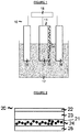
- a photodetector device 20 which comprises particles 21 of a compound of formula (I) according to the invention.
- This device comprises a layer 22 FTO of thickness of the order of 500 nm on which is electrodeposed a layer 23 of thickness of the order 1 micron based on ZnO.
- the layer 24 of thickness of the order of 1 ⁇ m based on the particles 21 of a compound of formula (I) according to the invention is deposited on the surface of the layer 23 by depositing drops from a suspension of particles of a compound of formula (I) according to the invention at 25-30% by weight in ethanol.
- the photovoltaic device 30 which comprises particles 31 of a compound of formula (I) according to the invention.
- This device comprises a layer 32 FTO with a thickness of the order of 500 nm on which is electrodeposed a layer 33 of thickness of the order 1 microns based on ZnO.
- the layer 34 with a thickness of around 1 ⁇ m based on the particles 31 of a compound of formula (I) according to the invention is deposited on the surface of the layer 33 by depositing drops from a suspension of particles of formula (I) according to the invention at 25-30% by weight in ethanol.
- An electrolyte containing the pair of I 2 / I - 35 mediator redox is deposited by depositing drops on the surface of the layer 34, and on which a gold layer 36 of thickness of the order of 1 micron being deposited by evaporation.
- the photovoltaic device 40 which comprises a layer 41 based on particles of a compound of formula (I) according to the invention deposited on a layer 42 based on ZnO by coating, the layer 42 based on ZnO being prepared by the sol-gel deposition, the layer 41 being in contact with a layer 43 of gold and the layer 42 based on the ZnO being in contact with an FTO layer 44.
- a compound of formula (I) according to the invention Contacting a compound of formula (I) according to the invention with a n-type ZnO semiconductor forms a p-n junction.
- the electrons generated go into the ZnO and the holes generated remain in the compound of formula (I) according to the invention.
- ZnO is in contact with FTO (electron conductor) to extract the electrons and the compound of formula (I) according to the invention is in contact with gold (conductor holes) to extract the holes.
- FTO electron conductor
- the mortar is then covered and placed in a Fritsch No. 6 planetary mill with a rotation speed of the order of 500 rpm. The grinding is continued for 120 min until a pure phase is obtained.
- the device described on the Figure 1 polarizing the working electrode to a potential of -0.8 V vs Ag / AgCl.
- the system is irradiated under an incandescent lamp (whose color temperature is 2700 K) alternating periods of darkness and periods of light.
- the intensity of the current increased when the system was placed in the light. It is a photocurrent measured at 100 ⁇ A.cm -2 , which confirms the ability of the compound C 1 to generate a photocurrent.
- This photocurrent is cathodic (that is to say negative) which is consistent with the fact that this compound C 1 is a p-type semiconductor.
Landscapes
- Chemical & Material Sciences (AREA)
- Organic Chemistry (AREA)
- Inorganic Chemistry (AREA)
- Engineering & Computer Science (AREA)
- Power Engineering (AREA)
- Physics & Mathematics (AREA)
- Electromagnetism (AREA)
- Materials Engineering (AREA)
- Microelectronics & Electronic Packaging (AREA)
- Photovoltaic Devices (AREA)
- Hybrid Cells (AREA)
- Inorganic Compounds Of Heavy Metals (AREA)
- Manufacturing & Machinery (AREA)
- Condensed Matter Physics & Semiconductors (AREA)
- General Physics & Mathematics (AREA)
Description
- La présente invention a trait au domaine des composés inorganiques semi-conducteurs, en particulier destinés à fournir un photocourant, notamment par effet photovoltaïques.
- De nos jours, les technologies photovoltaïques employant des composés inorganiques sont principalement fondées sur les technologies du silicium (plus de 80% du marché) et sur les technologies dites « couche mince » (principalement le CdTe et le CIGS (Cuivre Indium Gallium Sélénium), représentant 20% du marché). La croissance du marché du photovoltaïque semble exponentielle (40 GW cumulés en 2010, 67 GW cumulés en 2011).
- Malheureusement, ces technologies souffrent d'inconvénients limitant leur capacité à satisfaire ce marché grandissant. Ces inconvénients incluent une mauvaise flexibilité pour ce qui est du silicium d'un point de vue mécanique et d'installation, et la toxicité et la rareté des éléments pour les technologies « couche mince ». En particulier, le cadmium, le tellure et le sélénium sont toxiques. Par ailleurs, l'indium et le tellure sont rares, ce qui se répercute notamment sur leur coût.
- Pour ces raisons, on cherche à s'affranchir de la mise en oeuvre de l'indium, du cadmium, du tellure et du sélénium ou à diminuer leur proportion.
- Une voie qui a été préconisée pour remplacer l'indium dans le CIGS est de le remplacer par le couple (Zn2+, Sn4+). Dans ce cadre, il a été notamment proposé le composé Cu2ZnSnSe4 (dit CZTS). Ce matériau est aujourd'hui considéré comme le plus sérieux successeur du CIGS en termes d'efficacité, mais qui présente l'inconvénient de toxicité du sélénium.
- Pour ce qui est du sélénium et du tellure, peu de solutions de substitution ont été proposées et elles s'avèrent généralement peu intéressantes. Les composés comme le SnS, le FeS2 et le Cu2S ont bien été testés mais, bien qu'ils aient des propriétés intrinsèques intéressantes (gap, conductivité...), ils ne s'avèrent pas assez stables chimiquement (ex : le Cu2S se transforme très facilement en Cu2O au contact de l'air et de l'humidité).
WO 2014/049172 A2 divulgue des oxydes et sulfures mixtes de bismuth et cuivre pour application photovoltaïque. -
WO 2010/024500 A1 divulgue un composé de formule Bi1-xMxCuwOa-yQ1yTeb-zQ2z, où M est au moins un élément choisi du groupe comprenant Ba, Sr, Ca, Mg, Cs, K, Na, Cd, Hg, Sn, Pb, Eu, Sm, Mn, Ga, In, TI, As et Sb; Q1 et Q2 sont au moins un élément choisi du groupe comprenant S, Se, As et Sb avec 0<=x<1, 0<w<=1, 0.2<a<4, 0<=y<4, 0.2<b<4 and 0<=z<4. - A ce jour, à la connaissance des inventeurs, il n'a pas été publié de solution satisfaisante permettant d'obtenir une bonne efficacité photovoltaïque sans problèmes liés à la toxicité et/ou la rareté des éléments employés dans un système photovoltaïque.
- Un but de la présente invention est justement de fournir des composés inorganiques alternatifs à ceux utilisés dans les technologies photovoltaïques actuelles, qui permettent d'éviter les problèmes précités.
- A cet effet, la présente invention propose d'utiliser une nouvelle famille de matériaux inorganiques, dont les inventeurs ont maintenant mis en évidence que, de façon inattendue, ils s'avèrent présenter une bonne efficacité, et qu'ils présentent l'avantage de ne pas avoir à utiliser, ou à une très faible teneur, des métaux rares ou toxiques du type In, Te, Cd précités, et offrent en outre la possibilité d'employer des anions, tels que Se ou Te, en une teneur réduite, voire de ne pas utiliser ce type d'anions.
- L'un des objets de la présente invention est un nouveau matériau comprenant au moins un composé de formule (I) :
Bi1-xMxAg1-y-εM'yOS1-zM"z (I)
dans lequel - M est un élément ou un mélange d'éléments choisis dans le groupe (A) constitué par Pb, Sn, Hg, Ca, Sr, Ba, Sb, In, Tl, Mg, les terres rares,
- M' est un élément ou un mélange d'éléments choisis dans le groupe (B) constitué par Ti, V, Cr, Mn, Fe, Co, Ni, Cu, Zn, Ga, Al, Cd, Pt, Pd,
- M" est un halogène,
- x, y et z sont des nombres inférieurs à 1, en particulier inférieurs à 0,6, notamment inférieurs à 0,5, par exemple inférieurs à 0,2,

- Lorsqu'ils sont présents, les éléments M, M' et M" sont généralement des éléments de substitution occupant respectivement la place de l'élément Bi, de l'élément Ag et de l'élément S.
- Par « matériau comprenant au moins un composé de formule (I) », on entend un solide, généralement sous forme divisée (poudre, dispersion) ou sous forme d'un revêtement ou d'une couche continue ou discontinue sur un support, et qui comprend, voire consiste en, un composé répondant à la formule (I).
- Par « terre rare », on entend les éléments du groupe constitué par l'yttrium et le scandium et les éléments de la classification périodique de numéro atomique compris inclusivement entre 57 et 71.
- Selon un premier mode de réalisation, les nombres x, y et z sont nuls (x = y = z = 0). Ainsi, le composé de formule (I) selon l'invention répond à la formule suivante : BiAg1-εOS.
- Selon un second mode de réalisation de l'invention, au moins un des nombres x, y ou z est non nul.
- Selon ce second mode de réalisation de l'invention, l'élément M peut de préférence être choisi parmi les éléments Sb, Pb, Ba et les terres rares. L'élément M peut par exemple être du lutécium.
- L'élément M' peut de préférence être choisi parmi les éléments Cu, Zn, Mn. L'élément M' peut par exemple être l'élément Cu.
- L'élément M" peut notamment être l'élément I.
- Dans une première variante de ce second mode de réalisation de l'invention, le composé de formule (I) selon l'invention répond à la formule suivante : Bi1-xMxAg1-εOS (Ia), où x ≠ 0, ε est un nombre nul ou non nul et M est un élément ou un mélange d'éléments choisis dans le groupe (A) constitué par Pb, Sn, Hg, Ca, Sr, Ba, Sb, In, TI, Mg, les terres rares.
- Selon un mode de réalisation de cette variante de l'invention, M est un élément ou un mélange d'éléments choisis parmi les terres rares.
- Le composé peut alors par exemple répondre à la formule Bi1-xLuxAgOS où x ≠ 0 et ε = 0.
- Dans une deuxième variante de l'invention, le composé de formule (I) selon l'invention répond à la formule suivante : BiAg1-y-εM'yOS (Ib), où y ≠ 0, ε est un nombre nul ou non nul et M' est un élément ou un mélange d'éléments choisis dans le groupe (B) constitué par Ti, V, Cr, Mn, Fe, Co, Ni, Cu, Zn, Ga, Al, Cd, Pt, Pd.
- Selon un mode de réalisation de cette variante de l'invention, M' est un élément ou un mélange d'éléments choisis parmi les éléments Cu et Zn.
- Le composé peut alors par exemple répondre à la formule BiAg1-yCuyOS ou à la formule BiAg1-yZnyOS où y ≠ 0 et ε = 0.
- Dans une troisième variante de l'invention, le composé de formule (I) selon l'invention répond à la formule suivante : BiAgOSzM"1-z (Ic), où z ≠ 0, ε est un nombre nul ou non nul et M" est un halogène.
- Selon un mode de réalisation de cette variante de l'invention, M" est l'élément I, et le composé répond alors à la formule BiAgOSzI1-z où z ≠ 0 et ε = 0.
- L'invention a également pour objet un procédé de préparation du matériau selon l'invention comprenant une étape de broyage solide d'un mélange comprenant au moins des composés inorganiques de bismuth et d'argent, et
éventuellement au moins un oxyde, sulfure, oxysulfure, halogénure ou oxyhalogénure d'au moins un élément choisi parmi Bi et les éléments du groupe (A) constitué par Pb, Sn, Hg, Ca, Sr, Ba, Sb, In, TI, Mg, les terres rares, et
éventuellement au moins un oxyde, sulfure, oxysulfure, halogénure ou oxyhalogénure d'au moins un élément choisi parmi Ag et les éléments du groupe (B) constitué par Ti, V, Cr, Mn, Fe, Co, Ni, Cu, Zn, Ga, Al, Cd, Pt, Pd. - Selon l'invention, on broie un mélange sous forme solide comprenant au moins des composés inorganiques de bismuth et d'argent. De préférence, les composés inorganiques de bismuth et d'argent présents dans le mélange sont au moins les composés Bi2O3, Bi2S3 et Ag2S.
- Ce broyage peut se faire selon tout moyen connu en soi. Ce mélange peut notamment être placé dans un mortier en agate. Le broyage peut par exemple être réalisé avec un broyeur planétaire.
- Pour faciliter le broyage, il est possible d'ajouter au mélange sous forme solide des billes de broyage qui consistent par exemple en des billes en acier inoxydable, des billes en acier spécial au chrome, des billes en agate, des billes en carbure de tungstène, des billes en oxyde de zirconium.
- Le temps de broyage peut être ajusté selon le produit recherché. Il peut notamment être compris entre 20 minutes et 96 heures, notamment entre 1 heure et 72 heures.
- Les composés inorganiques de bismuth et d'argent dans le mélange peuvent se présenter sous la forme de particules présentant une granulométrie inférieure à 50 µm, en particulier inférieure à 10 µm, par exemple inférieure à 1 µm.
- Les dimensions de particules auxquelles il est fait référence ici peuvent typiquement être mesurées par microscopie électronique à balayage (MEB).
- La présente invention a en outre pour objet l'utilisation d'un matériau comprenant au moins d'un composé de formule (I) :
Bi1-xMxAg1-y-εM'yOS1-zM"z (I)
dans lequel - M est un élément ou un mélange d'éléments choisis dans le groupe (A) constitué par Pb, Sn, Hg, Ca, Sr, Ba, Sb, In, Tl, Mg, les terres rares,
- M' est un élément ou un mélange d'éléments choisis dans le groupe (B) constitué par Ti, V, Cr, Mn, Fe, Co, Ni, Cu, Zn, Ga, Al, Cd, Pt, Pd.
- M" est un halogène,
- x, y et z sont des nombres inférieurs à 1, en particulier inférieurs à 0,6, notamment inférieurs à 0,5, par exemple inférieurs à 0,2, et

- Ce qui est indiqué dans l'exposé ci-dessus, notamment au sujet des éléments M, M' et M" et des nombres x, y et z s'applique à la présente utilisation selon l'invention.
- Le composé qui est présent dans le matériau semi-conducteur est un matériau inorganique substitué, notamment du type p.
- Les substitutions chimiques du bismuth, d'argent et/ou du soufre peuvent avoir plusieurs rôles.
- Dans le cas de substitutions isoélectroniques telles que la substitution de l'élément Bi par des terres rares ou par l'élément Sb ou bien encore la substitution de l'élément Ag par l'élément Cu, ces substitutions peuvent, notamment en modifiant les paramètres de maille et/ou en modifiant l'extension des orbitales et leur position énergétique, ainsi entraîner des modifications du gap (bande de valence - bande de conduction).
- Les substitutions aliovalentes modifient quant à elles le degré d'oxydation de l'élément Ag.
- L'introduction de substituants dans la structure du semi-conducteur peut, selon le cas, entraîner une réduction ou une augmentation du nombre de porteurs de charges. Les matériaux substitués peuvent notamment présenter une conductivité plus élevée, qui induit une capacité de conduction améliorée, par rapport à sa forme non substituée, ou au contraire une conductivité plus faible.
- Dans le cadre de la présente invention, les inventeurs ont maintenant mis en évidence que les matériaux répondant à la formule (I) précitée, en particulier, lorsqu'ils sont de type p, sont capables de fournir un photocourant lorsqu'ils sont irradiés sous une longueur d'onde supérieure à leur gap (à savoir la génération d'une paire électron-trou au sein du matériau sous l'effet d'un photon incident d'énergie suffisante, les espèces chargées formées (l'électron et le « trou », à savoir la lacune d'électron) étant libres de se déplacer pour engendrer un courant).
- En particulier, les inventeurs ont maintenant mis en évidence que les matériaux de l'invention s'avèrent propres à assurer un effet photovoltaïque.
- De façon générale, un effet photovoltaïque est obtenu par mise en oeuvre conjointe de deux composés semi-conducteurs de type distincts, à savoir :
- un premier composé présentant un caractère semi-conducteur de type p ; et
- un deuxième composé présentant un caractère semi-conducteur de type n.
- Dans le cadre de l'invention, l'effet photovoltaïque est typiquement obtenu en plaçant un matériau à base d'un semi-conducteur de formule (I) précitée, qui est en outre spécifiquement de type p, en contact avec un semi-conducteur de type n entre deux électrodes, en contact direct ou éventuellement connectés au moins à une des électrodes par l'intermédiaire d'un revêtement supplémentaire, par exemple un revêtement collecteur de charge ; et en irradiant le dispositif photovoltaïque ainsi réalisée par un rayonnement électromagnétique adéquat, typiquement par la lumière du spectre solaire. Pour ce faire, il est préférable qu'une des électrodes laisse passer le rayonnement électromagnétique employé.
- Selon un autre aspect particulier, la présente invention a pour objet les dispositifs photovoltaïques comprenant, entre un matériau conducteur de trous et un matériau conducteur d'électrons, une couche à base d'un composé de formule (I) de type p et une couche à base d'un semi-conducteur de type n, où :
- la couche à base du composé de formule (I) est en contact avec la couche à base du semi-conducteur de type n ;
- la couche à base du composé de formule (I) est à proximité du matériau conducteur de trous ; et
- la couche à base du semi-conducteur de type n est à proximité du matériau conducteur d'électrons.
- Par « matériau conducteur de trous » au sens de la présente description, on entend un matériau qui est capable d'assurer une circulation du courant entre le semi-conducteur de type p et le circuit électrique.
- Le semi-conducteur de type n employé dans les dispositifs photovoltaïques selon l'invention peut être choisi parmi tout semi-conducteur qui présente un caractère accepteur d'électrons plus marqué que le composé de formule (I) ou un composé favorisant l'évacuation des électrons. De préférence, le semi-conducteur de type n peut être un oxyde, par exemple ZnO, ou TiO2, ou un sulfure, par exemple ZnS.
- Le matériau conducteur de trous employé dans les dispositifs photovoltaïques selon l'invention peut être par exemple un métal adapté, comme l'or, le tungstène, ou le molybdène ; ou un métal déposé sur un support, ou en contact avec un électrolyte, tel que Pt/FTO (platine déposé sur du dioxyde d'étain dopé au fluor) ; ou un oxyde conducteur comme de l'ITO (oxyde d'indium dopé étain), par exemple, déposé sur du verre ; ou un polymère conducteur de type p.
- Selon un mode de réalisation particulier, le matériau conducteur de trous peut comprendre un matériau conducteur de trous du type précité et un médiateur rédox, par exemple un électrolyte contenant le couple I2/I-, dans quel cas, le matériau conducteur de trous est typiquement Pt/FTO.
- Le matériau conducteur d'électrons peut être, par exemple FTO, ou AZO (oxyde de zinc dopé aluminium), ou un semi-conducteur de type n.
- Dans un dispositif photovoltaïque selon l'invention, les trous générés à la jonction p-n sont extraits via le matériau conducteur de trous et les électrons sont extraits via le matériau conducteur d'électrons du type précités.
- Dans un dispositif photovoltaïque selon l'invention, il est préférable que le matériau conducteur de trous et/ou le matériau conducteur d'électrons soit un matériau au moins partiellement transparent qui permet de laisser passer le rayonnement électromagnétique employé. Dans ce cas, le matériau au moins partiellement transparent est avantageusement placé entre la source du rayonnement électromagnétique incident et le semi-conducteur de type p.
- A cet effet, le matériau conducteur de trous peut par exemple être un matériau choisi parmi un métal ou un verre conducteur.
- Alternativement ou conjointement, le matériau conducteur d'électrons peut être au moins partiellement transparent, et on le choisit alors par exemple parmi FTO (dioxyde d'étain dopé au fluor), ou AZO (oxyde de zinc dopé aluminium), ou un semi-conducteur de type n.
- Selon un autre mode de réalisation intéressant, la couche à base d'un semi-conducteur de type n qui est en contact avec la couche à base d'un composé de formule (I) de type p peut en outre être au moins partiellement transparente.
- Par « matériau partiellement transparent », on entend ici un matériau qui laisse passer une partie au moins du rayonnement électromagnétique incident, utile pour fournir le photocourant, et qui peut être :
- un matériau qui n'absorbe pas totalement le champ électromagnétique incident ; et/ou
- un matériau qui est sous une forme ajourée (comportant typiquement des trous, des fentes ou des interstices) propre à laisser passer une partie du rayonnement électromagnétique sans que celui-ci rencontre le matériau.
- Le composé de formule (I) employé selon la présente invention est avantageusement utilisé sous la forme d'objets isotropes ou anisotropes ayant au moins une dimension inférieure à 50 µm, de préférence inférieure à 20 µm, typiquement inférieure à 10 µm, préférentiellement inférieure à 5 µm, généralement inférieure à 1 µm, plus avantageusement inférieure à 500 nm, par exemple inférieure à 200 nm, voire à 100 nm.
- Typiquement, la dimension inférieure à 50 µm peut être :
- le diamètre moyen dans le cas d'objets isotropes ;
- l'épaisseur ou le diamètre transversal dans le cas d'objets anisotropes.
- Selon une première variante, les objets à base d'un composé de formule (I) sont des particules, ayant typiquement des dimensions inférieures à 10 µm.
- Ces particules sont de préférence obtenues selon l'un des procédés de préparation de l'invention.
- Par « particules », on entend ici des objets isotropes ou anisotropes, qui peuvent être des particules individuelles, ou bien des agrégats.
- Les dimensions des particules auxquelles il est fait référence ici peuvent typiquement être mesurées par microscopie électronique à balayage (MEB).
- Avantageusement, le composé de formule (I) est sous la forme de particules anisotropes de type plaquette, ou d'agglomérats de quelques dizaines à quelques centaines de particules de ce type, ces particules de type plaquette ayant typiquement des dimensions restant inférieures à 5 µm, (préférentiellement inférieures à 1 µm, plus avantageusement inférieures à 500 nm), avec une épaisseur qui reste typiquement inférieure à 500 nm, par exemple inférieure à 100 nm.
- Les particules du type décrit selon la première variante peuvent typiquement être employées à l'état déposé sur un support conducteur ou semi-conducteur de type n.
- Une plaque d'ITO ou de métal recouverte de particules de formule (I) de type p selon l'invention peut ainsi, par exemple jouer le rôle d'une électrode photoactive pour un dispositif de type photoélectrochimique qui peut être utilisé notamment comme photodétecteur.
- Typiquement, un dispositif de type photoélectrochimique mettant en oeuvre une électrode photoactive du type précité, comprend un électrolyte qui est généralement une solution de sel, par exemple, une solution de KCI, ayant typiquement une concentration de l'ordre de 1 M, dans lequel sont plongées :
- une électrode photoactive du type précité (plaque d'ITO ou métal recouverts de particules de composé de formule (I) selon l'invention) ;
- une électrode de référence ; et
- une contre-électrode ;
- Selon un mode de réalisation possible, le dispositif électrochimique peut comprendre :
- à titre d'électrode photoactive : un support (tel qu'une plaque d'ITO) recouvert des particules de composé de formule (I);
- à titre d'électrode de référence : par exemple, une électrode Ag/AgCl ; et
- à titre de contre-électrode : par exemple, un fil de platine ;
- Lorsqu'un dispositif électrochimique de ce type est placé sous une source lumineuse, sous l'effet d'irradiation, des paires électrons-trous se forment et sont dissociées.
- Lorsque l'électrolyte est une solution aqueuse, ce qui est le plus souvent le cas, l'eau dans l'électrolyte est réduite à proximité de l'électrode photoactive par les électrons générés, produisant de l'hydrogène et des ions OH-. Les ions OH- ainsi produits vont migrer vers la contre-électrode via l'électrolyte ; et les trous du composé de formule (I) vont être extraits via le conducteur du type ITO et vont entrer dans le circuit électrique externe. Finalement, l'oxydation des OH- se réalise à l'aide des trous à proximité de la contre-électrode en produisant de l'oxygène. La mise en mouvement de ces charges (trous et électrons), induite par l'absorption de la lumière du composé de formule (I), génère un photocourant.
- Le dispositif peut notamment être utilisé comme photodétecteur, le photocourant n'étant généré que lorsque le dispositif est éclairé.
- Une électrode photoactive telle que décrite ci-dessus peut notamment être réalisée en employant une suspension, comprenant les particules d'un composé de formule (I) du type précité dispersés dans un solvant, et en déposant cette suspension sur un support, par exemple une plaque de verre recouvert d'ITO ou une plaque de métal, par la voie humide ou toute méthode d'enduction, par exemple, par dépôt de gouttes (« drop-casting » en anglais), centrifugation (« spin-coating » en anglais), trempage (« dip-coating » en anglais), jet d'encre ou encore par sérigraphie. Pour plus de détail à ce sujet, on pourra se reporter à l'article : R. M. Pasquarelli, D. S. Ginley, R. O'Hayre, dans Chem. Soc. Rev., vol 40, pp. 5406-5441, 2011. De préférence, les particules à base d'un composé de formule (I) qui sont présentes dans la suspension ont un diamètre moyen tel que mesuré par granulométrie laser (par exemple, au moyen d'une granulométrie laser de type Malvern) qui est inférieur à 5 µm.
- Selon un mode de réalisation préférentiel, les particules de composé de formule (I) peuvent être préalablement dispersées dans un solvant, par exemple, le terpineol ou l'éthanol.
- La suspension contenant les particules de composé de formule (I) peut être déposée sur un support, par exemple une plaque recouverte d'oxyde conducteur.
- Selon une deuxième variante de l'invention qui se révèle bien adaptée à la réalisation de dispositifs photovoltaïques, le composé de formule (I) est sous la forme d'une couche continue à base du composé de formule (I) dont l'épaisseur est inférieure à 50 µm, de préférence inférieure à 20 µm, plus avantageusement inférieure à 10 µm, par exemple inférieure à 5 µm et typiquement supérieure à 500 nm.
- Par « couche continue », on entend ici un dépôt homogène réalisé sur un support et recouvrant ledit support, non obtenu par un simple dépôt d'une dispersion de particules sur le support.
- La couche continue à base d'un composé de formule (I) de type p selon cette variante particulière de l'invention est typiquement placée à proximité d'une couche d'un semi-conducteur de type n, entre un matériau conducteur de trous et un matériau conducteur d'électrons, pour former un dispositif photovoltaïque destiné à fournir un effet photovoltaïque.
- Un semi-conducteur de type n dans l'utilisation selon l'invention peut être un oxyde conducteur, par exemple ZnO, ou TiO2, ou un sulfure, par exemple ZnS.
- Par ailleurs, on entend par couche « à base du composé de formule (I) » une couche comprenant du composé de formule (I), de préférence à raison d'au moins 50% en masse, voire à raison d'au moins 75% en masse.
- Selon un mode de réalisation, la couche continue selon la deuxième variante est essentiellement constituée par du composé de formule (I), et elle comprend typiquement au moins 95% en masse, voire au moins 98% en masse, plus préférentiellement au moins 99% en masse du composé de formule (I).
- La couche continue à base d'un composé de formule (I) employé selon ce mode de réalisation peut prendre plusieurs formes.
- La couche continue peut notamment comprendre une matrice polymère et, dispersées au sein de cette matrice, des particules à base d'un composé de formule (I), typiquement de dimensions inférieures à 10 µm, voire inférieure à 5 µm, notamment du type de celles employées dans le premier mode de l'invention.
- Typiquement, la matrice polymère comprend un polymère conducteur de type p, qui peut notamment être choisi parmi les dérivés du polythiophène, plus particulièrement parmi les dérivés du poly(3,4-ethylènedioxythiophène):poly(styrènesulfonate) (PEDOT:PSS).
- Les particules à base du composé de formule (I) présentes dans la matrice polymère ont de préférence, des dimensions inférieures à 5 µm, qui peuvent notamment être déterminées par MEB.
- L'invention va maintenant être illustrée plus en détails, en référence aux exemples illustratifs donnés ci-après et aux Figures ci-annexées, sur lesquelles :
- la
Figure 1 est une représentation schématique en coupe d'une cellule photoélectrochimique utilisée dans l'exemple 2 décrit ci-après ; - la
Figure 2 est une représentation schématique en coupe d'un dispositif photodétecteur ; - la
Figure 3 est une représentation schématique en coupe d'un dispositif photovoltaïque ; - la
Figure 4 est une représentation schématique en coupe d'un dispositif photovoltaïque selon l'invention, non exemplifié. - Sur la
Figure 1 est représentée une cellule photoélectrochimique 10 qui comprend : - une électrode photoactive 11 constituée par un support 12 à base d'un verre recouvert d'une couche conductrice d'ITO de 2 cm x 1 cm sur lequel a été déposé sur toute la surface une couche 13 d'épaisseur de l'ordre de 1 µm à base de particules 14 d'un composé de formule (I) selon l'invention, les particules 14 ont été préalablement dispersées dans du terpinéol puis déposées par enduction (« Doctor Blade Coating » en anglais) sur la plaque de verre conducteur 11.
- une électrode de référence (Ag/AgCl) 15 ; et
- une contre-électrode (fil de platine) 16 ;
- Sur la
Figure 2 est représenté un dispositif photodétecteur 20 qui comprend des particules 21 d'un composé de formule (I) selon l'invention. Ce dispositif comprend une couche 22 FTO d'épaisseur de l'ordre de 500 nm sur laquelle est électrodéposée une couche 23 d'épaisseur de l'ordre 1 µm à base de ZnO. La couche 24 d'épaisseur de l'ordre de 1 µm à base des particules 21 d'un composé de formule (I) selon l'invention est déposée à la surface de la couche 23 par dépôt des gouttes à partir d'une suspension de particules d'un composé de formule (I) selon l'invention à 25-30% en masse dans l'éthanol. Une couche d'or 25 d'épaisseur de l'ordre de 1 µm déposée sur la couche 24 par évaporation. - Sur la
Figure 3 est représenté le dispositif photovoltaïque 30 qui comprend des particules 31 d'un composé de formule (I) selon l'invention. Ce dispositif comprend une couche 32 FTO d'épaisseur de l'ordre de 500 nm sur laquelle est électrodéposée une couche 33 d'épaisseur de l'ordre 1 µm à base de ZnO. La couche 34 d'épaisseur de l'ordre de 1 µm à base des particules 31 d'un composé de formule (I) selon l'invention est déposée à la surface de la couche 33 par dépôt des gouttes à partir d'une suspension de particules de formule (I) selon l'invention à 25-30% en masse dans l'éthanol. Un électrolyte contenant le couple de I2/I- 35 servant de médiateur redox est déposé par dépôt des gouttes sur la surface de la couche 34, et sur lequel une couche d'or 36 d'épaisseur de l'ordre de 1 µm étant déposée par évaporation. - Sur la
Figure 4 est représenté le dispositif photovoltaïque 40 qui comprend une couche 41 à base de particules d'un composé de formule (i) selon l'invention déposées sur une couche 42 à base de ZnO par enduction, la couche 42 à base de ZnO étant préparée par la dépôt sol-gel, la couche 41 étant en contact avec d'une couche 43 d'or et la couche 42 à base du ZnO étant en contact avec une couche FTO 44. - La mise en contact d'un composé de formule (I) selon l'invention avec un semi-conducteur de type n ZnO forme une jonction p-n. Lorsque le dispositif est placé sous une source lumineuse, les électrons générés vont dans le ZnO et les trous générés restent dans le composé de formule (I) selon l'invention. Le ZnO est en contact avec du FTO (conducteur des électrons) pour en extraire les électrons et le composé de formule (I) selon l'invention est en contact avec de l'or (conducteur des trous) pour en extraire les trous.
- Les exemples suivants illustrent l'invention sans toutefois en limiter la portée.
- On a préparé une poudre de BiAgOS par broyage réactif à température ambiante, selon le protocole suivant :
- 0,685 g de Bi2S3, 1,243 g de Bi2O3 et 0,991 g de Ag2S sont placés dans un mortier en agate en présence de billes de broyage en agate.
- Le mortier est alors couvert et placé dans un broyeur planétaire de type Fritsch N° 6 avec une vitesse de rotation de l'ordre de 500 tr/min. Le broyage se poursuit pendant 120 min jusqu'à l'obtention d'une phase pure.
- Le composé obtenu C1 caractérisé par diffraction des rayons X présente les paramètres de maille tétragonale suivants : a = 3,92 Å, c = 9,23 Å, V = 141,7 Å3.
- On a utilisé le dispositif décrit sur la
Figure 1 , en polarisant l'électrode de travail à un potentiel de -0,8 V vs Ag/AgCl. Le système est irradié sous une lampe à incandescence (dont la température de couleur est à 2700 K) alternant des périodes d'obscurité et des périodes lumineuses. L'intensité du courant a augmenté lorsque le système a été placé à la lumière. Il s'agit d'un photocourant mesuré à 100 µA.cm-2, ce qui confirme l'aptitude du composé C1 à générer un photocourant. Ce photocourant est cathodique (c'est-à-dire négatif) ce qui est en accord avec le fait que ce composé C1 est un semi-conducteur de type p.
Claims (11)
- Matériau comprenant au moins un composé de formule (I) :
Bi1-xMxAg1-y-εM'yOS1-zM"z (I)
dans lequelM est un élément ou un mélange d'éléments choisis dans le groupe (A) constitué par Pb, Sn, Hg, Ca, Sr, Ba, Sb, In, Tl, Mg, les terres rares,M' est un élément ou un mélange d'éléments choisis dans le groupe (B) constitué par Ti, V, Cr, Mn, Fe, Co, Ni, Cu, Zn, Ga, Al, Cd, Pt, Pd,M" est un halogène,
x, y et z sont des nombres inférieurs à 1, en particulier inférieurs à 0,6, notamment inférieurs à 0,5, et
- Matériau selon la revendication 1, dans lequel les nombres x, y et z sont nuls, ce par quoi le composé de formule (I) répond à la formule suivante :BiAg1-εOS
- Matériau selon la revendication 1, dans lequel au moins un des nombres x, y ou z est non nul.
- Procédé de préparation d'un matériau selon l'une des revendications 1 à 3, comprenant une étape de broyage solide d'un mélange comprenant au moins des composés inorganiques de bismuth et d'argent, et
éventuellement au moins un oxyde, sulfure, oxysulfure, halogénure ou oxyhalogènure d'au moins un élément choisi parmi Bi et les éléments du groupe (A), et,
éventuellement au moins un oxyde, sulfure, oxysulfure, halogénure ou oxyhalogénure d'au moins un élément choisi parmi Ag et les éléments du groupe (B). - Utilisation d'un matériau selon l'une des revendications 1 à 3 à titre de semi-conducteur, notamment pour application photoélectrochimique ou photochimique, en particulier pour fournir un photocourant.
- Utilisation selon la revendication 5, où le composé de formule (I) est employé sous la forme d'objets isotropes ou anisotropes ayant au moins une dimension inférieure à 50 µm, de préférence inférieure à 20 µm.
- Utilisation selon la revendication 6, où le composé de formule (I) est employé sous la forme de particules de dimensions inférieures à 10 µm.
- Utilisation selon la revendication 7 où le composé de formule (I) est sous la forme de particules anisotropes de type plaquette, ou d'agglomérats de quelques dizaines à quelques centaines de particules de ce type.
- Utilisation selon la revendication 6, où le composé de formule (I) est sous la forme d'une couche continue à base d'un composé de formule (I) dont l'épaisseur est inférieure à 50 µm, de préférence inférieure à 20 µm, où la couche à base d'un composé de formule (I) est une couche comprenant du composé de formule (I) à raison d'au moins du 95% en masse.
- Utilisation selon la revendication 6, où le composé de formule (I) est sous la forme d'une couche continue à base d'un composé de formule (I) dont l'épaisseur est inférieure à 50 µm, de préférence inférieure à 20 µm, où la couche à base d'un composé de formule (I) comprend une matrice polymère et, dispersées au sein de cette matrice, des particules à base d'un composé de formule (I) de dimensions inférieures à 5 µm.
- Dispositif photovoltaïque comprenant, entre un matériau conducteur de trous et un matériau conducteur d'électrons, une couche à base d'un composé de formule (I) selon l'une des revendications 1 à 3, de type p, et une couche à base d'un semi-conducteur de type n, où :- la couche à base du composé de formule (I) de type p est en contact avec la couche à base du semi-conducteur de type n ;- la couche à base du composé de formule (I) de type p est à proximité du matériau conducteur de trous ; et- la couche à base du semi-conducteur de type n est à proximité du matériau conducteur d'électrons.
Applications Claiming Priority (2)
| Application Number | Priority Date | Filing Date | Title |
|---|---|---|---|
| FR1400833A FR3019540A1 (fr) | 2014-04-04 | 2014-04-04 | Oxydes et sulfures mixtes de bismuth et argent pour application photovoltaique |
| PCT/EP2015/097024 WO2015150592A1 (fr) | 2014-04-04 | 2015-04-03 | Oxydes et sulfures mixtes de bismuth et argent pour application photovoltaique |
Publications (2)
| Publication Number | Publication Date |
|---|---|
| EP3126293A1 EP3126293A1 (fr) | 2017-02-08 |
| EP3126293B1 true EP3126293B1 (fr) | 2018-03-21 |
Family
ID=51518811
Family Applications (1)
| Application Number | Title | Priority Date | Filing Date |
|---|---|---|---|
| EP15720356.3A Not-in-force EP3126293B1 (fr) | 2014-04-04 | 2015-04-03 | Oxydes et sulfures mixtes de bismuth et argent pour application photovoltaique |
Country Status (8)
| Country | Link |
|---|---|
| US (1) | US10593817B2 (fr) |
| EP (1) | EP3126293B1 (fr) |
| JP (1) | JP6562999B2 (fr) |
| KR (1) | KR20160142321A (fr) |
| CN (1) | CN106488885B (fr) |
| ES (1) | ES2673934T3 (fr) |
| FR (1) | FR3019540A1 (fr) |
| WO (1) | WO2015150592A1 (fr) |
Families Citing this family (1)
| Publication number | Priority date | Publication date | Assignee | Title |
|---|---|---|---|---|
| FR3019539B1 (fr) * | 2014-04-04 | 2016-04-29 | Rhodia Operations | Oxydes et sulfures mixtes de bismuth et cuivre pour application photovoltaique |
Family Cites Families (7)
| Publication number | Priority date | Publication date | Assignee | Title |
|---|---|---|---|---|
| EP1547160A1 (fr) * | 2002-08-13 | 2005-06-29 | Agfa-Gevaert | Semiconducteur a oxyde metallique nanoporeux spectralement sensibilise a l'aide de nanoparticules de chalcogenure metallique |
| BRPI0414001A (pt) * | 2003-09-12 | 2006-10-24 | Univ Michigan State | material semicondutor, material termoelétrico, processo de fabricar um material condutivo e método de sua formulação, e método para gerar energia elétrica a partir de energia térmica |
| WO2010024500A1 (fr) * | 2008-08-29 | 2010-03-04 | Lg Chem, Ltd. | Nouveau composé semi-conducteur et son procédé de fabrication, pile solaire et élément de conversion thermoélectrique l’utilisant |
| KR102038170B1 (ko) * | 2012-03-19 | 2019-10-29 | 넥스닷 | 평탄한 이방성의 콜로이드성 반도체 나노결정들을 포함하는 발광 디바이스 및 이러한 디바이스의 제조 방법 |
| US20130287976A1 (en) * | 2012-04-26 | 2013-10-31 | Integran Technologies Inc. | Anisotropic elongated metallic structural member |
| FR2996355B1 (fr) * | 2012-09-28 | 2016-04-29 | Rhodia Operations | Oxydes et sulfures mixtes de bismuth et cuivre pour application photovoltaique |
| KR101614062B1 (ko) * | 2013-10-04 | 2016-04-20 | 주식회사 엘지화학 | 신규한 화합물 반도체 및 그 활용 |
-
2014
- 2014-04-04 FR FR1400833A patent/FR3019540A1/fr not_active Withdrawn
-
2015
- 2015-04-03 JP JP2017503075A patent/JP6562999B2/ja not_active Expired - Fee Related
- 2015-04-03 US US15/301,494 patent/US10593817B2/en not_active Expired - Fee Related
- 2015-04-03 CN CN201580016777.XA patent/CN106488885B/zh not_active Expired - Fee Related
- 2015-04-03 WO PCT/EP2015/097024 patent/WO2015150592A1/fr not_active Ceased
- 2015-04-03 KR KR1020167029120A patent/KR20160142321A/ko not_active Withdrawn
- 2015-04-03 ES ES15720356.3T patent/ES2673934T3/es active Active
- 2015-04-03 EP EP15720356.3A patent/EP3126293B1/fr not_active Not-in-force
Also Published As
| Publication number | Publication date |
|---|---|
| FR3019540A1 (fr) | 2015-10-09 |
| US10593817B2 (en) | 2020-03-17 |
| ES2673934T3 (es) | 2018-06-26 |
| CN106488885A (zh) | 2017-03-08 |
| JP2017513804A (ja) | 2017-06-01 |
| KR20160142321A (ko) | 2016-12-12 |
| CN106488885B (zh) | 2018-04-06 |
| JP6562999B2 (ja) | 2019-08-21 |
| US20170110605A1 (en) | 2017-04-20 |
| EP3126293A1 (fr) | 2017-02-08 |
| WO2015150592A1 (fr) | 2015-10-08 |
Similar Documents
| Publication | Publication Date | Title |
|---|---|---|
| Garnier et al. | Physical properties of annealed ZnO nanowire/CuSCN heterojunctions for self-powered UV photodetectors | |
| Wang et al. | Synthesis of shape-controlled monodisperse wurtzite CuIn x Ga1–x S2 semiconductor nanocrystals with tunable band gap | |
| EP2674516A1 (fr) | Méthode de fabrication de nanofils de CuSCN par voie électrochimique | |
| FR2996355A1 (fr) | Oxydes et sulfures mixtes de bismuth et cuivre pour application photovoltaique | |
| EP3126292A1 (fr) | Oxydes et sulfures mixtes de bismuth et cuivre pour application photovoltaïque | |
| Park et al. | Efficient eco-friendly inverted quantum dot sensitized solar cells | |
| Lee et al. | Plasmonic behaviour and plasmon-induced charge separation of nanostructured MoO3− x under near infrared irradiation | |
| EP3114704B1 (fr) | Procédé de préparation de couche mince d'absorbeur a base de sulfure(s) et séléniures(s) de cuivre, zinc et étain, couche mince recuite et dispositif photovoltaïque obtenus | |
| US20150318119A1 (en) | Cation-exchanged quantum dot photoanodes and solar cells | |
| Bie et al. | Close-spaced sublimation of CdZnTe: In films for solar energy water splitting | |
| FR3001467A1 (fr) | Procede de preparation de couche mince d'absorbeur a base de sulfure(s) de cuivre, zinc et etain, couche mince recuite et dispositif photovoltaique obtenu | |
| Lee et al. | Induced growth of CsPbBr3 perovskite films by incorporating metal chalcogenide quantum dots in PbBr2 films for performance enhancement of inorganic perovskite solar cells | |
| CA2732559C (fr) | Elaboration de couche d'oxyde transparente et conductrice pour utilisation dans une structure photovoltaique | |
| Alhammadi et al. | Effect of Gallium doping on CdS thin film properties and corresponding Cu (InGa) Se2/CdS: Ga solar cell performance | |
| Esparza et al. | Current improvement in hybrid quantum dot sensitized solar cells by increased light-scattering with a polymer layer | |
| Eskandari et al. | Enhanced photovoltaic performance of a cadmium sulfide/cadmium selenide-sensitized solar cell using an aluminum-doped zinc oxide electrode | |
| Resende et al. | An investigation of photovoltaic devices based on p‐type Cu2O and n‐type γ‐WO3 junction through an electrolyte solution containing a redox pair | |
| EP3126293A1 (fr) | Oxydes et sulfures mixtes de bismuth et argent pour application photovoltaique | |
| Ahmad et al. | Enhanced optoelectrical performance of ultraviolet detectors based on self-assembled porous zinc oxide nanostructures | |
| Kassim et al. | Effects of Deposition Potential on Cu4SnS4 Thin Films Prepared by Electrodeposition | |
| JPWO2014136562A1 (ja) | 化合物半導体超微粒子、超微粒子薄膜及び光電変換デバイス | |
| EP3080332B1 (fr) | Bain à persulfate et procédé pour le dépôt chimique d'une couche | |
| Kirsanova | Engineering of Semiconductor Nanocomposites for Harvesting and Routing of Optical Energy | |
| FR2899724A1 (fr) | Dispositifs photovoltaiques tout solides comportant une couche d'absorbeur a base de sulfure de bismuth ou de sulfure d'etain |
Legal Events
| Date | Code | Title | Description |
|---|---|---|---|
| STAA | Information on the status of an ep patent application or granted ep patent |
Free format text: STATUS: THE INTERNATIONAL PUBLICATION HAS BEEN MADE |
|
| PUAI | Public reference made under article 153(3) epc to a published international application that has entered the european phase |
Free format text: ORIGINAL CODE: 0009012 |
|
| STAA | Information on the status of an ep patent application or granted ep patent |
Free format text: STATUS: REQUEST FOR EXAMINATION WAS MADE |
|
| 17P | Request for examination filed |
Effective date: 20161104 |
|
| AK | Designated contracting states |
Kind code of ref document: A1 Designated state(s): AL AT BE BG CH CY CZ DE DK EE ES FI FR GB GR HR HU IE IS IT LI LT LU LV MC MK MT NL NO PL PT RO RS SE SI SK SM TR |
|
| AX | Request for extension of the european patent |
Extension state: BA ME |
|
| DAV | Request for validation of the european patent (deleted) | ||
| DAX | Request for extension of the european patent (deleted) | ||
| GRAP | Despatch of communication of intention to grant a patent |
Free format text: ORIGINAL CODE: EPIDOSNIGR1 |
|
| STAA | Information on the status of an ep patent application or granted ep patent |
Free format text: STATUS: GRANT OF PATENT IS INTENDED |
|
| INTG | Intention to grant announced |
Effective date: 20171025 |
|
| GRAS | Grant fee paid |
Free format text: ORIGINAL CODE: EPIDOSNIGR3 |
|
| GRAA | (expected) grant |
Free format text: ORIGINAL CODE: 0009210 |
|
| STAA | Information on the status of an ep patent application or granted ep patent |
Free format text: STATUS: THE PATENT HAS BEEN GRANTED |
|
| AK | Designated contracting states |
Kind code of ref document: B1 Designated state(s): AL AT BE BG CH CY CZ DE DK EE ES FI FR GB GR HR HU IE IS IT LI LT LU LV MC MK MT NL NO PL PT RO RS SE SI SK SM TR |
|
| REG | Reference to a national code |
Ref country code: GB Ref legal event code: FG4D Free format text: NOT ENGLISH |
|
| REG | Reference to a national code |
Ref country code: CH Ref legal event code: EP |
|
| REG | Reference to a national code |
Ref country code: AT Ref legal event code: REF Ref document number: 980879 Country of ref document: AT Kind code of ref document: T Effective date: 20180415 |
|
| REG | Reference to a national code |
Ref country code: IE Ref legal event code: FG4D Free format text: LANGUAGE OF EP DOCUMENT: FRENCH |
|
| REG | Reference to a national code |
Ref country code: DE Ref legal event code: R096 Ref document number: 602015009118 Country of ref document: DE |
|
| REG | Reference to a national code |
Ref country code: FR Ref legal event code: PLFP Year of fee payment: 4 |
|
| REG | Reference to a national code |
Ref country code: ES Ref legal event code: FG2A Ref document number: 2673934 Country of ref document: ES Kind code of ref document: T3 Effective date: 20180626 |
|
| REG | Reference to a national code |
Ref country code: NL Ref legal event code: FP |
|
| PG25 | Lapsed in a contracting state [announced via postgrant information from national office to epo] |
Ref country code: LT Free format text: LAPSE BECAUSE OF FAILURE TO SUBMIT A TRANSLATION OF THE DESCRIPTION OR TO PAY THE FEE WITHIN THE PRESCRIBED TIME-LIMIT Effective date: 20180321 Ref country code: CY Free format text: LAPSE BECAUSE OF FAILURE TO SUBMIT A TRANSLATION OF THE DESCRIPTION OR TO PAY THE FEE WITHIN THE PRESCRIBED TIME-LIMIT Effective date: 20180321 Ref country code: HR Free format text: LAPSE BECAUSE OF FAILURE TO SUBMIT A TRANSLATION OF THE DESCRIPTION OR TO PAY THE FEE WITHIN THE PRESCRIBED TIME-LIMIT Effective date: 20180321 Ref country code: NO Free format text: LAPSE BECAUSE OF FAILURE TO SUBMIT A TRANSLATION OF THE DESCRIPTION OR TO PAY THE FEE WITHIN THE PRESCRIBED TIME-LIMIT Effective date: 20180621 Ref country code: FI Free format text: LAPSE BECAUSE OF FAILURE TO SUBMIT A TRANSLATION OF THE DESCRIPTION OR TO PAY THE FEE WITHIN THE PRESCRIBED TIME-LIMIT Effective date: 20180321 |
|
| REG | Reference to a national code |
Ref country code: LT Ref legal event code: MG4D |
|
| REG | Reference to a national code |
Ref country code: AT Ref legal event code: MK05 Ref document number: 980879 Country of ref document: AT Kind code of ref document: T Effective date: 20180321 |
|
| PG25 | Lapsed in a contracting state [announced via postgrant information from national office to epo] |
Ref country code: RS Free format text: LAPSE BECAUSE OF FAILURE TO SUBMIT A TRANSLATION OF THE DESCRIPTION OR TO PAY THE FEE WITHIN THE PRESCRIBED TIME-LIMIT Effective date: 20180321 Ref country code: GR Free format text: LAPSE BECAUSE OF FAILURE TO SUBMIT A TRANSLATION OF THE DESCRIPTION OR TO PAY THE FEE WITHIN THE PRESCRIBED TIME-LIMIT Effective date: 20180622 Ref country code: BG Free format text: LAPSE BECAUSE OF FAILURE TO SUBMIT A TRANSLATION OF THE DESCRIPTION OR TO PAY THE FEE WITHIN THE PRESCRIBED TIME-LIMIT Effective date: 20180621 Ref country code: LV Free format text: LAPSE BECAUSE OF FAILURE TO SUBMIT A TRANSLATION OF THE DESCRIPTION OR TO PAY THE FEE WITHIN THE PRESCRIBED TIME-LIMIT Effective date: 20180321 Ref country code: SE Free format text: LAPSE BECAUSE OF FAILURE TO SUBMIT A TRANSLATION OF THE DESCRIPTION OR TO PAY THE FEE WITHIN THE PRESCRIBED TIME-LIMIT Effective date: 20180321 |
|
| PG25 | Lapsed in a contracting state [announced via postgrant information from national office to epo] |
Ref country code: MT Free format text: LAPSE BECAUSE OF FAILURE TO SUBMIT A TRANSLATION OF THE DESCRIPTION OR TO PAY THE FEE WITHIN THE PRESCRIBED TIME-LIMIT Effective date: 20180321 |
|
| PG25 | Lapsed in a contracting state [announced via postgrant information from national office to epo] |
Ref country code: AL Free format text: LAPSE BECAUSE OF FAILURE TO SUBMIT A TRANSLATION OF THE DESCRIPTION OR TO PAY THE FEE WITHIN THE PRESCRIBED TIME-LIMIT Effective date: 20180321 Ref country code: EE Free format text: LAPSE BECAUSE OF FAILURE TO SUBMIT A TRANSLATION OF THE DESCRIPTION OR TO PAY THE FEE WITHIN THE PRESCRIBED TIME-LIMIT Effective date: 20180321 Ref country code: RO Free format text: LAPSE BECAUSE OF FAILURE TO SUBMIT A TRANSLATION OF THE DESCRIPTION OR TO PAY THE FEE WITHIN THE PRESCRIBED TIME-LIMIT Effective date: 20180321 Ref country code: PL Free format text: LAPSE BECAUSE OF FAILURE TO SUBMIT A TRANSLATION OF THE DESCRIPTION OR TO PAY THE FEE WITHIN THE PRESCRIBED TIME-LIMIT Effective date: 20180321 |
|
| PG25 | Lapsed in a contracting state [announced via postgrant information from national office to epo] |
Ref country code: SK Free format text: LAPSE BECAUSE OF FAILURE TO SUBMIT A TRANSLATION OF THE DESCRIPTION OR TO PAY THE FEE WITHIN THE PRESCRIBED TIME-LIMIT Effective date: 20180321 Ref country code: CZ Free format text: LAPSE BECAUSE OF FAILURE TO SUBMIT A TRANSLATION OF THE DESCRIPTION OR TO PAY THE FEE WITHIN THE PRESCRIBED TIME-LIMIT Effective date: 20180321 Ref country code: SM Free format text: LAPSE BECAUSE OF FAILURE TO SUBMIT A TRANSLATION OF THE DESCRIPTION OR TO PAY THE FEE WITHIN THE PRESCRIBED TIME-LIMIT Effective date: 20180321 Ref country code: AT Free format text: LAPSE BECAUSE OF FAILURE TO SUBMIT A TRANSLATION OF THE DESCRIPTION OR TO PAY THE FEE WITHIN THE PRESCRIBED TIME-LIMIT Effective date: 20180321 |
|
| REG | Reference to a national code |
Ref country code: CH Ref legal event code: PL |
|
| PG25 | Lapsed in a contracting state [announced via postgrant information from national office to epo] |
Ref country code: PT Free format text: LAPSE BECAUSE OF FAILURE TO SUBMIT A TRANSLATION OF THE DESCRIPTION OR TO PAY THE FEE WITHIN THE PRESCRIBED TIME-LIMIT Effective date: 20180723 |
|
| REG | Reference to a national code |
Ref country code: DE Ref legal event code: R097 Ref document number: 602015009118 Country of ref document: DE |
|
| REG | Reference to a national code |
Ref country code: IE Ref legal event code: MM4A |
|
| PLBE | No opposition filed within time limit |
Free format text: ORIGINAL CODE: 0009261 |
|
| STAA | Information on the status of an ep patent application or granted ep patent |
Free format text: STATUS: NO OPPOSITION FILED WITHIN TIME LIMIT |
|
| PG25 | Lapsed in a contracting state [announced via postgrant information from national office to epo] |
Ref country code: MC Free format text: LAPSE BECAUSE OF FAILURE TO SUBMIT A TRANSLATION OF THE DESCRIPTION OR TO PAY THE FEE WITHIN THE PRESCRIBED TIME-LIMIT Effective date: 20180321 Ref country code: LU Free format text: LAPSE BECAUSE OF NON-PAYMENT OF DUE FEES Effective date: 20180403 Ref country code: DK Free format text: LAPSE BECAUSE OF FAILURE TO SUBMIT A TRANSLATION OF THE DESCRIPTION OR TO PAY THE FEE WITHIN THE PRESCRIBED TIME-LIMIT Effective date: 20180321 |
|
| 26N | No opposition filed |
Effective date: 20190102 |
|
| PG25 | Lapsed in a contracting state [announced via postgrant information from national office to epo] |
Ref country code: LI Free format text: LAPSE BECAUSE OF NON-PAYMENT OF DUE FEES Effective date: 20180430 Ref country code: CH Free format text: LAPSE BECAUSE OF NON-PAYMENT OF DUE FEES Effective date: 20180430 |
|
| PG25 | Lapsed in a contracting state [announced via postgrant information from national office to epo] |
Ref country code: IE Free format text: LAPSE BECAUSE OF NON-PAYMENT OF DUE FEES Effective date: 20180403 |
|
| PG25 | Lapsed in a contracting state [announced via postgrant information from national office to epo] |
Ref country code: SI Free format text: LAPSE BECAUSE OF FAILURE TO SUBMIT A TRANSLATION OF THE DESCRIPTION OR TO PAY THE FEE WITHIN THE PRESCRIBED TIME-LIMIT Effective date: 20180321 |
|
| PG25 | Lapsed in a contracting state [announced via postgrant information from national office to epo] |
Ref country code: TR Free format text: LAPSE BECAUSE OF FAILURE TO SUBMIT A TRANSLATION OF THE DESCRIPTION OR TO PAY THE FEE WITHIN THE PRESCRIBED TIME-LIMIT Effective date: 20180321 |
|
| PGFP | Annual fee paid to national office [announced via postgrant information from national office to epo] |
Ref country code: NL Payment date: 20200312 Year of fee payment: 6 Ref country code: GB Payment date: 20200325 Year of fee payment: 6 |
|
| PGFP | Annual fee paid to national office [announced via postgrant information from national office to epo] |
Ref country code: BE Payment date: 20200316 Year of fee payment: 6 |
|
| PG25 | Lapsed in a contracting state [announced via postgrant information from national office to epo] |
Ref country code: MK Free format text: LAPSE BECAUSE OF NON-PAYMENT OF DUE FEES Effective date: 20180321 Ref country code: HU Free format text: LAPSE BECAUSE OF FAILURE TO SUBMIT A TRANSLATION OF THE DESCRIPTION OR TO PAY THE FEE WITHIN THE PRESCRIBED TIME-LIMIT; INVALID AB INITIO Effective date: 20150403 |
|
| PGFP | Annual fee paid to national office [announced via postgrant information from national office to epo] |
Ref country code: FR Payment date: 20200312 Year of fee payment: 6 |
|
| PG25 | Lapsed in a contracting state [announced via postgrant information from national office to epo] |
Ref country code: IS Free format text: LAPSE BECAUSE OF FAILURE TO SUBMIT A TRANSLATION OF THE DESCRIPTION OR TO PAY THE FEE WITHIN THE PRESCRIBED TIME-LIMIT Effective date: 20180721 |
|
| PGFP | Annual fee paid to national office [announced via postgrant information from national office to epo] |
Ref country code: ES Payment date: 20200504 Year of fee payment: 6 Ref country code: DE Payment date: 20200325 Year of fee payment: 6 |
|
| PGFP | Annual fee paid to national office [announced via postgrant information from national office to epo] |
Ref country code: IT Payment date: 20200312 Year of fee payment: 6 |
|
| REG | Reference to a national code |
Ref country code: DE Ref legal event code: R081 Ref document number: 602015009118 Country of ref document: DE Owner name: RHODIA OPERATIONS, FR Free format text: FORMER OWNERS: LE CENTRE NATIONAL DE LA RECHERCHE SCIENTIFIQUE, PARIS, FR; RHODIA OPERATIONS, PARIS, FR Ref country code: DE Ref legal event code: R081 Ref document number: 602015009118 Country of ref document: DE Owner name: LE CENTRE NATIONAL DE LA RECHERCHE SCIENTIFIQU, FR Free format text: FORMER OWNERS: LE CENTRE NATIONAL DE LA RECHERCHE SCIENTIFIQUE, PARIS, FR; RHODIA OPERATIONS, PARIS, FR |
|
| REG | Reference to a national code |
Ref country code: DE Ref legal event code: R119 Ref document number: 602015009118 Country of ref document: DE |
|
| REG | Reference to a national code |
Ref country code: NL Ref legal event code: MM Effective date: 20210501 |
|
| GBPC | Gb: european patent ceased through non-payment of renewal fee |
Effective date: 20210403 |
|
| REG | Reference to a national code |
Ref country code: BE Ref legal event code: MM Effective date: 20210430 |
|
| PG25 | Lapsed in a contracting state [announced via postgrant information from national office to epo] |
Ref country code: GB Free format text: LAPSE BECAUSE OF NON-PAYMENT OF DUE FEES Effective date: 20210403 Ref country code: FR Free format text: LAPSE BECAUSE OF NON-PAYMENT OF DUE FEES Effective date: 20210430 Ref country code: DE Free format text: LAPSE BECAUSE OF NON-PAYMENT OF DUE FEES Effective date: 20211103 |
|
| PG25 | Lapsed in a contracting state [announced via postgrant information from national office to epo] |
Ref country code: NL Free format text: LAPSE BECAUSE OF NON-PAYMENT OF DUE FEES Effective date: 20210501 |
|
| REG | Reference to a national code |
Ref country code: ES Ref legal event code: FD2A Effective date: 20220629 |
|
| PG25 | Lapsed in a contracting state [announced via postgrant information from national office to epo] |
Ref country code: ES Free format text: LAPSE BECAUSE OF NON-PAYMENT OF DUE FEES Effective date: 20210404 Ref country code: BE Free format text: LAPSE BECAUSE OF NON-PAYMENT OF DUE FEES Effective date: 20210430 |
|
| PG25 | Lapsed in a contracting state [announced via postgrant information from national office to epo] |
Ref country code: IT Free format text: LAPSE BECAUSE OF NON-PAYMENT OF DUE FEES Effective date: 20200403 |
|
| PG25 | Lapsed in a contracting state [announced via postgrant information from national office to epo] |
Ref country code: IT Free format text: LAPSE BECAUSE OF NON-PAYMENT OF DUE FEES Effective date: 20210403 |