EP3125024A1 - Display device housing with draining hole for moisture - Google Patents
Display device housing with draining hole for moisture Download PDFInfo
- Publication number
- EP3125024A1 EP3125024A1 EP15203067.2A EP15203067A EP3125024A1 EP 3125024 A1 EP3125024 A1 EP 3125024A1 EP 15203067 A EP15203067 A EP 15203067A EP 3125024 A1 EP3125024 A1 EP 3125024A1
- Authority
- EP
- European Patent Office
- Prior art keywords
- supporting portion
- display device
- display panel
- back cover
- middle cabinet
- Prior art date
- Legal status (The legal status is an assumption and is not a legal conclusion. Google has not performed a legal analysis and makes no representation as to the accuracy of the status listed.)
- Granted
Links
Images



Classifications
-
- G—PHYSICS
- G02—OPTICS
- G02F—OPTICAL DEVICES OR ARRANGEMENTS FOR THE CONTROL OF LIGHT BY MODIFICATION OF THE OPTICAL PROPERTIES OF THE MEDIA OF THE ELEMENTS INVOLVED THEREIN; NON-LINEAR OPTICS; FREQUENCY-CHANGING OF LIGHT; OPTICAL LOGIC ELEMENTS; OPTICAL ANALOGUE/DIGITAL CONVERTERS
- G02F1/00—Devices or arrangements for the control of the intensity, colour, phase, polarisation or direction of light arriving from an independent light source, e.g. switching, gating or modulating; Non-linear optics
- G02F1/01—Devices or arrangements for the control of the intensity, colour, phase, polarisation or direction of light arriving from an independent light source, e.g. switching, gating or modulating; Non-linear optics for the control of the intensity, phase, polarisation or colour
- G02F1/13—Devices or arrangements for the control of the intensity, colour, phase, polarisation or direction of light arriving from an independent light source, e.g. switching, gating or modulating; Non-linear optics for the control of the intensity, phase, polarisation or colour based on liquid crystals, e.g. single liquid crystal display cells
- G02F1/133—Constructional arrangements; Operation of liquid crystal cells; Circuit arrangements
- G02F1/1333—Constructional arrangements; Manufacturing methods
- G02F1/133308—Support structures for LCD panels, e.g. frames or bezels
-
- H—ELECTRICITY
- H05—ELECTRIC TECHNIQUES NOT OTHERWISE PROVIDED FOR
- H05K—PRINTED CIRCUITS; CASINGS OR CONSTRUCTIONAL DETAILS OF ELECTRIC APPARATUS; MANUFACTURE OF ASSEMBLAGES OF ELECTRICAL COMPONENTS
- H05K5/00—Casings, cabinets or drawers for electric apparatus
- H05K5/02—Details
- H05K5/03—Covers
-
- G—PHYSICS
- G02—OPTICS
- G02F—OPTICAL DEVICES OR ARRANGEMENTS FOR THE CONTROL OF LIGHT BY MODIFICATION OF THE OPTICAL PROPERTIES OF THE MEDIA OF THE ELEMENTS INVOLVED THEREIN; NON-LINEAR OPTICS; FREQUENCY-CHANGING OF LIGHT; OPTICAL LOGIC ELEMENTS; OPTICAL ANALOGUE/DIGITAL CONVERTERS
- G02F1/00—Devices or arrangements for the control of the intensity, colour, phase, polarisation or direction of light arriving from an independent light source, e.g. switching, gating or modulating; Non-linear optics
- G02F1/01—Devices or arrangements for the control of the intensity, colour, phase, polarisation or direction of light arriving from an independent light source, e.g. switching, gating or modulating; Non-linear optics for the control of the intensity, phase, polarisation or colour
- G02F1/13—Devices or arrangements for the control of the intensity, colour, phase, polarisation or direction of light arriving from an independent light source, e.g. switching, gating or modulating; Non-linear optics for the control of the intensity, phase, polarisation or colour based on liquid crystals, e.g. single liquid crystal display cells
- G02F1/133—Constructional arrangements; Operation of liquid crystal cells; Circuit arrangements
- G02F1/1333—Constructional arrangements; Manufacturing methods
- G02F1/133308—Support structures for LCD panels, e.g. frames or bezels
- G02F1/133311—Environmental protection, e.g. against dust or humidity
-
- G—PHYSICS
- G02—OPTICS
- G02F—OPTICAL DEVICES OR ARRANGEMENTS FOR THE CONTROL OF LIGHT BY MODIFICATION OF THE OPTICAL PROPERTIES OF THE MEDIA OF THE ELEMENTS INVOLVED THEREIN; NON-LINEAR OPTICS; FREQUENCY-CHANGING OF LIGHT; OPTICAL LOGIC ELEMENTS; OPTICAL ANALOGUE/DIGITAL CONVERTERS
- G02F1/00—Devices or arrangements for the control of the intensity, colour, phase, polarisation or direction of light arriving from an independent light source, e.g. switching, gating or modulating; Non-linear optics
- G02F1/01—Devices or arrangements for the control of the intensity, colour, phase, polarisation or direction of light arriving from an independent light source, e.g. switching, gating or modulating; Non-linear optics for the control of the intensity, phase, polarisation or colour
- G02F1/13—Devices or arrangements for the control of the intensity, colour, phase, polarisation or direction of light arriving from an independent light source, e.g. switching, gating or modulating; Non-linear optics for the control of the intensity, phase, polarisation or colour based on liquid crystals, e.g. single liquid crystal display cells
- G02F1/133—Constructional arrangements; Operation of liquid crystal cells; Circuit arrangements
- G02F1/1333—Constructional arrangements; Manufacturing methods
- G02F1/133308—Support structures for LCD panels, e.g. frames or bezels
- G02F1/133314—Back frames
-
- G—PHYSICS
- G02—OPTICS
- G02F—OPTICAL DEVICES OR ARRANGEMENTS FOR THE CONTROL OF LIGHT BY MODIFICATION OF THE OPTICAL PROPERTIES OF THE MEDIA OF THE ELEMENTS INVOLVED THEREIN; NON-LINEAR OPTICS; FREQUENCY-CHANGING OF LIGHT; OPTICAL LOGIC ELEMENTS; OPTICAL ANALOGUE/DIGITAL CONVERTERS
- G02F1/00—Devices or arrangements for the control of the intensity, colour, phase, polarisation or direction of light arriving from an independent light source, e.g. switching, gating or modulating; Non-linear optics
- G02F1/01—Devices or arrangements for the control of the intensity, colour, phase, polarisation or direction of light arriving from an independent light source, e.g. switching, gating or modulating; Non-linear optics for the control of the intensity, phase, polarisation or colour
- G02F1/13—Devices or arrangements for the control of the intensity, colour, phase, polarisation or direction of light arriving from an independent light source, e.g. switching, gating or modulating; Non-linear optics for the control of the intensity, phase, polarisation or colour based on liquid crystals, e.g. single liquid crystal display cells
- G02F1/133—Constructional arrangements; Operation of liquid crystal cells; Circuit arrangements
- G02F1/1333—Constructional arrangements; Manufacturing methods
- G02F1/133308—Support structures for LCD panels, e.g. frames or bezels
- G02F1/133317—Intermediate frames, e.g. between backlight housing and front frame
-
- G—PHYSICS
- G02—OPTICS
- G02F—OPTICAL DEVICES OR ARRANGEMENTS FOR THE CONTROL OF LIGHT BY MODIFICATION OF THE OPTICAL PROPERTIES OF THE MEDIA OF THE ELEMENTS INVOLVED THEREIN; NON-LINEAR OPTICS; FREQUENCY-CHANGING OF LIGHT; OPTICAL LOGIC ELEMENTS; OPTICAL ANALOGUE/DIGITAL CONVERTERS
- G02F1/00—Devices or arrangements for the control of the intensity, colour, phase, polarisation or direction of light arriving from an independent light source, e.g. switching, gating or modulating; Non-linear optics
- G02F1/01—Devices or arrangements for the control of the intensity, colour, phase, polarisation or direction of light arriving from an independent light source, e.g. switching, gating or modulating; Non-linear optics for the control of the intensity, phase, polarisation or colour
- G02F1/13—Devices or arrangements for the control of the intensity, colour, phase, polarisation or direction of light arriving from an independent light source, e.g. switching, gating or modulating; Non-linear optics for the control of the intensity, phase, polarisation or colour based on liquid crystals, e.g. single liquid crystal display cells
- G02F1/133—Constructional arrangements; Operation of liquid crystal cells; Circuit arrangements
- G02F1/1333—Constructional arrangements; Manufacturing methods
- G02F1/1345—Conductors connecting electrodes to cell terminals
- G02F1/13452—Conductors connecting driver circuitry and terminals of panels
-
- H—ELECTRICITY
- H10—SEMICONDUCTOR DEVICES; ELECTRIC SOLID-STATE DEVICES NOT OTHERWISE PROVIDED FOR
- H10K—ORGANIC ELECTRIC SOLID-STATE DEVICES
- H10K59/00—Integrated devices, or assemblies of multiple devices, comprising at least one organic light-emitting element covered by group H10K50/00
- H10K59/10—OLED displays
Definitions
- the present invention relates to a display device, and more particularly, to a narrow bezel type display device in which an area of an outer rim of the display device is reduced or a borderless type display device in which an outer rim is removed.
- liquid crystal display device In general, although a liquid crystal display device, a plasma display device, a field emission display device, a light emitting display device, and the like are actively studied as a flat type display device, the liquid crystal display device and the light emitting display device having merits of mass production technology, easiness of driving means, and realization of high resolution are in the spotlight.
- FIG. 1 is a cross-sectional view illustrating a display device according to the related art.
- the display device according to the related art includes a display panel 105, a printed circuit board 113 which is electrically connected to the display panel with plural circuit films 111 and is arranged in parallel with the rear side of the display panel 105, and a back cover 101 which safely holds the display panel 105 by wrapping a bending portion of the circuit films 111 from the end of the display panel 105.
- the printed circuit board 113 is electrically connected to the plural circuit films 111 and supplies various signals for displaying an image on the display panel 105.
- a driving IC 117 for driving the display panel 105 and the like is embedded in the printed circuit board 113, a heat radiation pad 115 for radiating heat generated from the circuit films 111 and the printed circuit board 113 is coupled to the inner side of the back cover 101, and a heat radiation pad 119 for radiating heat by keeping a suitable space with the circuit films 111 is coupled to the lower part of the display panel 105.
- an object of the present invention in a display device having a small size or a large size, is to provide a display device in which decrease in thickness and decrease in weight can be contrived by considerably reducing a width of a front rim.
- Another object of the present invention in a display device having a small size or a large size, is to provide a display device in which plural circuit films and a printed circuit board and the like that are arranged in a circuit section coupled to the display panel can be protected by preventing inflow of moisture from the outside despite considerable reduction of a width of a front rim.
- a display device in which inflow of moisture from the outside can be prevented despite reduction of a width of a bezel of the display device by providing incisions in a middle cabinet and providing drain holes in a back cover, the middle cabinet and the back cover supporting the display panel.
- a display device may comprise a display panel; a middle cabinet including a first supporting portion and a second supporting portion that are substantially perpendicular to each other, wherein the second supporting portion protrudes from the first supporting portion and is configured to support the display panel, the second supporting portion having one or two corner incisions; and a back cover that is coupled to a rear surface of the second supporting portion and has a drain hole formed at one or both corners of the back cover to correspond to the one or two corner incisions of the middle cabinet.
- a corner in which a bottom part of the second supporting portion is coupled to a side part of the second supporting portion may be incised or cut in the middle cabinet.
- the middle cabinet may have a first step portion that is formed by incising an inner end of the second supporting portion in a direction of the first supporting portion. That is, the first step portion may be formed as an undercut in the second supporting portion, so that an extension width (i.e. width parallel to the display area or display panel and perpendicular to the first supporting portion) of the second supporting portion is reduced at the first step portion.
- the middle cabinet may further have a second step portion that is formed by further incising an end of the first step portion in the direction of the first supporting portion. Hence, the second step portion may be subsequent to the first step portion and closer to a corner of the middle portion than the first step portion.
- the second step portion of the second supporting portion may have a smaller extension width than the first step portion of the second supporting portion.
- the second step portion may be closer to the corner compared to the first step portion.
- the second step portion may correspond to the drain hole of the back cover.
- the middle cabinet may have an incision hole that is formed by further incising a corner portion in which a bottom portion of the second step portion of the second supporting portion is coupled to a side portion of the second step portion of the second supporting portion to expose the inner surface of the first supporting portion.
- An absorption member may be provided between the second step portion and the display panel, that is between a front surface of the second step portion, i.e. the surface of the second step portion supporting the display panel, and a rear surface of the display panel.
- the absorption member may be curved with wrapping the second step portion, i.e. the surface of the display panel opposite to the light emitting surface.
- the absorption member may be provided to wrap a rear surface of the back cover via the incision hole.
- a display device may comprise a display panel; a middle cabinet including a first supporting portion wrapping a side of an end of the display panel and a second supporting portion on which the display panel is mounted, the second supporting portion protruding inside from an inner surface of the first supporting portion and including one or two corner incisions; and a back cover coupled to a rear surface of the second supporting portion, and including at least one drain hole formed at a side corner of the back cover to correspond to the one or two corner incisions of the middle cabinet.
- the second supporting portion may include a first step portion that is formed by incising an inner end of the second supporting portion in a direction of the first supporting portion.
- the second supporting portion further includes a second step portion that is formed by further incising an end of the first step portion in the direction of the first supporting portion.
- the second step portion may be closer to the corner compared to the first step portion.
- the second step portion may correspond to the drain hole of the back cover.
- the middle cabinet may further include an incision hole that is formed by further incising a corner portion in which a bottom portion of the second step portion is coupled to a side portion of the second step portion to expose an inner surface of the first supporting portion.
- An absorption member may be provided between a front surface of the second step portion and a rear surface of the display panel.
- An absorption member may be provided configured to wrap a rear surface of the back cover via the incision hole.
- a display device comprises a display panel; a middle cabinet including a first supporting portion and a second supporting portion, wherein the second supporting portion protrudes from the first supporting portion and supports the display panel, the second supporting portion having at least one incision; and a back cover that is coupled to the second supporting portion and has at least one drain hole formed at at least one corner of the back cover.
- the second supporting portion extends parallel to a display area of the display panel, wherein a width of the second supporting portion in parallel to the display area is reduced at the incision.
- the second supporting portion may extend perpendicular to the first supporting portion, wherein a width of the second supporting portion perpendicular to the first supporting portion is reduced at the incision.
- the incision may include an incision hole, at which the second supporting portion is removed, such that the first supporting portion forms an edge portion of the incision hole.
- the middle cabinet may have a frame shape.
- the middle cabinet has a T-shaped or L-shaped cross-section formed by the first and second supporting portion.
- the display panel may be supported on a first surface of the second supporting portion.
- the back cover may be coupled to a second surface of the second supporting portion opposite to the first surface.
- the first supporting portion covers at least one or all four sides of the display panel and/or at least one or all four sides of the back cover. That is, the first supporting portion may extend perpendicular to the display area.
- the incision may be provided at a corner of the middle cabinet and/or the drain hole may be provided at a corner of the back cover.
- the incision may be provided at a lower side (i.e. bottom side) of the middle cabinet and/or the drain hole may be provided at a lower side (i.e. bottom side) of the back cover, e.g. near a circuit portion.
- moisture or fluid between the display panel and the middle cabinet may flow downwards in direction of gravity to the incision of the middle cabinet and the drain hole of the back cover.
- the drain hole of the back cover may be provided at a position corresponding to the incision of the middle cabinet, i.e. the drain hole and the incision may overlap.
- bottom end, bottom side, lower side etc. may refer to an upright position of the display device, i.e. a normal position of a television or the like during normal operation, when a user is watching the display device.
- rear surface and front surface may refer to surfaces parallel to a display area with respect to a viewing direction.
- first, second, A, B, (a), and (b) can be used to describe elements of the invention. These terms are merely used to distinguish one element from another element and the essence, order, sequence, number, or the like of the elements is not limited to the terms. If it is mentioned that an element is “coupled” or “connected” to another element, it should be understood that the element is directly coupled or connected to another element or still another element is “interposed” therebetween or the elements may be “coupled” or “connected” to each other with still another element interposed therebetween.
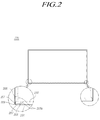
- FIG. 2 is a front view illustrating a middle cabinet of a display device according to an embodiment of the present invention
- FIG. 3 is a front view illustrating a back cover of a display device according to the embodiment of the present invention
- FIG. 4 is a cross-sectional view illustrating the display device according to the embodiment of the present invention
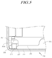
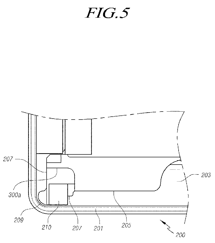
- FIG. 5 is a front view illustrating the display device according to the embodiment of the present invention, a display panel not being embedded therein
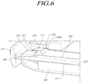
- FIG. 6 is a perspective view taken by partially-cutting a portion of FIG. 5 .
- a display device including a display panel 401, a middle cabinet 200 that is constituted by a first supporting portion 201 which wraps a side of an end of the display panel 401 and a second supporting portion 203 which protrudes inside from an inner surface of the first supporting portion 201 and the display panel 401 is mounted on the second supporting portion 203 having one or two corner incisions; and a back cover 300 that is coupled to a rear surface of the second supporting portion 203 and has a drain hole 300a formed at one or both corners thereof to correspond to the one or two corner incisions of the middle cabinet.
- inflow of moisture can be prevented or introduced moisture can be discharged despite a four-surface borderless type or a bezelless type in which a width of an outer rim, that is, a bezel is considerably reduced.
- the display panel 401 of the present invention may be a liquid crystal display panel or a light emitting display panel, e.g. an organic light emitting display panel.
- a backlight unit for illuminating a light on the liquid crystal display panel when the display panel is configured by the liquid crystal display panel, a backlight unit for illuminating a light on the liquid crystal display panel, a bottom polarizing plate attached to a lower substrate, and a top polarizing plate attached to the front of a top substrate may be further included.
- a driving mode of the liquid crystal display panel such as a Twisted Nematic (TN) mode, a Vertical Alignment (VA) mode, an In Plane Switching (IPS) mode, a Fringe Field Switching (FFS) mode
- TN Twisted Nematic
- VA Vertical Alignment
- IPS In Plane Switching
- FFS Fringe Field Switching
- the light emitting display panel is configured by including a bottom substrate which includes plural light emitting cells, each cell being formed in an every area defined by a gate line, a data line, and a power (VDD) line, and a top substrate which is combined with the bottom substrate to face thereto.
- VDD power
- each of the plural light emitting cells formed in the bottom substrate is configured by including at least one switching transistor coupled to the gate line and the data line, at least one driving transistor coupled to the switching transistor and the power (VDD) line, and a light emitting device (for example, an OLED) emitting light depending on current controlled by switching of the driving transistor, and the top substrate is configured to include a hygroscopic agent for protecting a light emitting device from moisture or oxygen in the air.
- a light emitting device coupled to the driving transistor may be further included in the top substrate, and in this case, a light emitting device of the bottom substrate may be omitted.
- the middle cabinet 200 supporting the display panel 401 of the present invention includes the first supporting portion 201 which wraps a side of an end of the display panel 401 and the second supporting portion 203 which protrudes inside from the inner side surface of the first supporting portion 201 and the display panel 401 is mounted on.
- the display panel 401 is mounted on the upper part of the second supporting portion 203 of the middle cabinet 200.
- the light emitting display panel is illustrated as an example in drawings, a backlight unit illuminating light to the panel is not configured due to configuration of illumination light by itself.
- FIG. 4 illustrating the light emitting display panel.
- encapsulation member 405 may adhere to the rear surface of the display panel 401 to seal the pixel array.
- the encapsulation member 405 may be a metal plate or a glass plate, and a polarizing film 403 may adhere to the entire surface of the display panel 401.
- side seal member 411 may be provided in the sides of the display panel 401.
- the side seal member 411 is formed by polymer materials in which black pigment is added, and the side seal member 411 absorbs light emitted from the pixel array, and thus light emitted through the sides of the display panel 401 cannot be seen.
- plural flexible circuit films 407 in which an IC is mounted are electrically connected to the display panel 401 in the rear surface of a bottom end or lower end of the display panel 401 having a rectangular shape, and a printed circuit board is provided in parallel with the display panel 401.
- the plural flexible circuit films 407 are attached to a pad portion and the printed circuit board by using a TAB (Tape Automated Bonding) process, and may be configured by a TCP (Tape Carrier Package) or a COF (Chip On Flexible board or Chip On Film).
- TAB Transmission Automated Bonding
- TCP Transmission Carrier Package
- COF Chip On Flexible board or Chip On Film
- the display panel 401 is electrically coupled or connected to the printed circuit board (not shown) via the plural flexible circuit films 407, and the printed circuit board is electrically coupled to the plural flexible circuit films 407 to provide various signals for displaying an image to the display panel 401.
- the middle cabinet 200 is configured by a first supporting portion 201 and a second supporting portion 203 that are perpendicular to each other, e.g. having a T-shaped cross-section.
- the first supporting portion 201 wraps the side of the end of the display panel 401 and is exposed to the front.
- the display panel 401 is mounted on the front surface of the second supporting portion 203, and the back cover 300 is coupled to the rear surface of the second supporting portion 203.
- the width of the bezel is considerably decreased, but there is the possibility that moisture may be introduced between the first supporting portion and the end of the panel 401.
- at least one side and/or at least one corner of the middle cabinet 200 may be incised, and at least one drain hole 300a may be formed in at least one side and/or at least one corner of the back cover 300.
- the at least one incision of the middle cabinet 200 and the at least one drain hole 300a of the back cover 300 may formed at corresponding positions.
- a moisture-proof and insulation member 409 (also known as a Tuffy) for protecting an IC and circuit elements of the flexible circuit film 407 is provided in a side surface and a rear surface of the flexible circuit film 407. Therefore, when moisture is introduced between the first supporting portion 201 and the end of the panel 401 and the moisture introduced from the outside is accumulated to be an amount, the moisture moves to the both sides due to a capillary phenomenon of a small space (about 0.6 to 0.8mm) among the first supporting portion 201, the display panel 401, the moisture-proof and insulation member 409, the second supporting portion 203, and the like.
- a corner of the middle cabinet 200, at which a bottom part of the second supporting portion 203 meets a side part of the second supporting portion 203 may be incised. Hence, the moisture which moves downwards to both bottom corners does not move to the flexible circuit film 407 and the printed circuit film and is drained to the outside via the incision portion 203a.
- first step portion 205 is formed in the middle cabinet 200 by incising an inner end of the second supporting portion 203 in the direction of the first supporting portion 201, the moisture moves to both bottom corner portions via a space between the moisture-proof and insulation member 409 and the second supporting portion 203. That is, the first step portion 205 may be formed extending towards a corner of the middle cabinet 200 by cutting a portion of the second supporting portion 203. Hence, a width of the second supporting portion 203 in the first step portion 205 may be reduced, as compared with the second supporting portion 203 without step portion, i.e. without incision. Then, the moisture does not move to the flexible circuit film 407 and the printed circuit film and flows into the first step portion 205.
- a second step portion 207 may also be formed in the middle cabinet 200 by further incising an inner end of the first step portion 205 in the direction of the first supporting portion 201.
- the second step portion 207 may be closer to a corner than the first step portion 205. That is, the second step portion 207 may be formed by cutting a portion of the second supporting portion 203 and may extend from the first step portion 205 towards a corner of the middle cabinet 200. Hence, a width of the second supporting portion 203 in the second step portion 207 may be further reduced than in the first step portion 205. Since the second step portion 207 is formed to correspond to the drain hole 300a of the back cover 300, moisture which flowed to the first step portion 205 is drained to the drain hole 300a via the second step portion 207.
- An incision hole 209 may be further formed in a corner area, e.g. a corner area to which the second step portion 207 of a lateral side of the second supporting portion 203 and the second step portion 207 of a bottom, i.e. lower side, of the second supporting portion 203 are coupled to expose the inner surface of the first supporting portion 201.
- An absorption member 210 may be combined between the front surface of the second step portion 207 and the rear surface of the display panel 401. Therefore, moisture which flowed downward from the second step portion 207 of the side of the second supporting portion 203 is not introduced into the bottom of second supporting portion 203 but drained to the drain hole 300a.
- the absorption member 210 is curved with wrapping the second step portion 207 and is combined to wrap the rear surface of the back cover 300, and thus the absorption member 210 absorbs the moisture which is gathered at the second step portion 207 of the side of the second supporting portion 203 and the second step portion 207 of the bottom of the second supporting portion 203. As a result, the moisture does not flow up to the flexible circuit film 407 and the printed circuit, and is drained to the outside of the back cover 300.
- the middle cabinet 200 and the back cover 300 may be bonded by using an adhesive member 211 such as an adhesive pad or a double-sided tape, and may be bonded with the display panel 401 via the adhesive member 211 such as the adhesive pad or the double-sided tape provided in the upper part of the second supporting portion 203.
- an adhesive member 211 such as an adhesive pad or a double-sided tape
- the flexible circuit film 407 is not provided in the other ends, so that there is no influence on the flexible circuit film 407. Therefore, an adhesive pad, a double-sided tape, or the like may be combined instead of the absorption member 210.
- the adhesive pad or the double-sided tape may use an adhesive thermal conductive tape.
- this middle cabinet 200 is formed by using synthetic resins such as plastics or metallic materials.
- the middle cabinet 220 is formed by using aluminum, aluminum alloy, stainless, stainless steel, zinc galvanizing steel plate, or the like.
Landscapes
- Physics & Mathematics (AREA)
- Nonlinear Science (AREA)
- Mathematical Physics (AREA)
- Chemical & Material Sciences (AREA)
- Crystallography & Structural Chemistry (AREA)
- General Physics & Mathematics (AREA)
- Optics & Photonics (AREA)
- Engineering & Computer Science (AREA)
- Microelectronics & Electronic Packaging (AREA)
- Devices For Indicating Variable Information By Combining Individual Elements (AREA)
Abstract
Description
- This application claims priority from and the benefit of Korean Patent Application No.
10-2015-0107136 filed on July 29, 2015 - The present invention relates to a display device, and more particularly, to a narrow bezel type display device in which an area of an outer rim of the display device is reduced or a borderless type display device in which an outer rim is removed.
- In general, although a liquid crystal display device, a plasma display device, a field emission display device, a light emitting display device, and the like are actively studied as a flat type display device, the liquid crystal display device and the light emitting display device having merits of mass production technology, easiness of driving means, and realization of high resolution are in the spotlight.
-
FIG. 1 is a cross-sectional view illustrating a display device according to the related art. As illustrated inFIG. 1 , the display device according to the related art includes adisplay panel 105, a printedcircuit board 113 which is electrically connected to the display panel withplural circuit films 111 and is arranged in parallel with the rear side of thedisplay panel 105, and aback cover 101 which safely holds thedisplay panel 105 by wrapping a bending portion of thecircuit films 111 from the end of thedisplay panel 105. - The printed
circuit board 113 is electrically connected to theplural circuit films 111 and supplies various signals for displaying an image on thedisplay panel 105. A driving IC 117 for driving thedisplay panel 105 and the like is embedded in theprinted circuit board 113, aheat radiation pad 115 for radiating heat generated from thecircuit films 111 and the printedcircuit board 113 is coupled to the inner side of theback cover 101, and aheat radiation pad 119 for radiating heat by keeping a suitable space with thecircuit films 111 is coupled to the lower part of thedisplay panel 105. - However, in the display device according to the related art, though an area of a bezel exposed to the front can be reduced, there is a problem that moisture is introduced into between an end of the back cover and an end of the display panel and the moisture flows to the circuit films and the printed circuit board, and thus a short circuit occurs and an error is generated.
- Particularly, when the short circuit and the error are generated, there is a problem that high cost and long repairing time are needed due to substitution of the whole display panel. Accordingly, in order to satisfy design requirements of a user, what is necessary is to develop a display device in which inflow of moisture from the outside can be prevented despite reduction of a width of an outer rim bezel.
- From this background, an object of the present invention, in a display device having a small size or a large size, is to provide a display device in which decrease in thickness and decrease in weight can be contrived by considerably reducing a width of a front rim.
- Another object of the present invention, in a display device having a small size or a large size, is to provide a display device in which plural circuit films and a printed circuit board and the like that are arranged in a circuit section coupled to the display panel can be protected by preventing inflow of moisture from the outside despite considerable reduction of a width of a front rim.
- Further, objects of the present invention are not limited thereto, and still another object of the present invention that is not mentioned can be understood by those skilled in the art from the following description. The objects are solved by the features of the independent claim.
- To accomplish the above-mentioned objects, there is provided a display device in which inflow of moisture from the outside can be prevented despite reduction of a width of a bezel of the display device by providing incisions in a middle cabinet and providing drain holes in a back cover, the middle cabinet and the back cover supporting the display panel.
- As described above, according to the present invention, in a display device having a small size or a large size, decrease in thickness and decrease in weight can be contrived by considerably reducing a width of a front rim
- Further, according to the present invention, in a display device having a small size or a large size, plural circuit films and a printed circuit board and the like which are arranged in a circuit section coupled to the display panel can be protected and manufacturing process can be shortened by preventing inflow of moisture from the outside despite considerable reduction of a width of a front rim.
- According to one example, a display device may comprise a display panel; a middle cabinet including a first supporting portion and a second supporting portion that are substantially perpendicular to each other, wherein the second supporting portion protrudes from the first supporting portion and is configured to support the display panel, the second supporting portion having one or two corner incisions; and a back cover that is coupled to a rear surface of the second supporting portion and has a drain hole formed at one or both corners of the back cover to correspond to the one or two corner incisions of the middle cabinet. A corner in which a bottom part of the second supporting portion is coupled to a side part of the second supporting portion may be incised or cut in the middle cabinet. The middle cabinet may have a first step portion that is formed by incising an inner end of the second supporting portion in a direction of the first supporting portion. That is, the first step portion may be formed as an undercut in the second supporting portion, so that an extension width (i.e. width parallel to the display area or display panel and perpendicular to the first supporting portion) of the second supporting portion is reduced at the first step portion. The middle cabinet may further have a second step portion that is formed by further incising an end of the first step portion in the direction of the first supporting portion. Hence, the second step portion may be subsequent to the first step portion and closer to a corner of the middle portion than the first step portion. The second step portion of the second supporting portion may have a smaller extension width than the first step portion of the second supporting portion. The second step portion may be closer to the corner compared to the first step portion. The second step portion may correspond to the drain hole of the back cover. The middle cabinet may have an incision hole that is formed by further incising a corner portion in which a bottom portion of the second step portion of the second supporting portion is coupled to a side portion of the second step portion of the second supporting portion to expose the inner surface of the first supporting portion. An absorption member may be provided between the second step portion and the display panel, that is between a front surface of the second step portion, i.e. the surface of the second step portion supporting the display panel, and a rear surface of the display panel. The absorption member may be curved with wrapping the second step portion, i.e. the surface of the display panel opposite to the light emitting surface. The absorption member may be provided to wrap a rear surface of the back cover via the incision hole.
- According to another example, a display device may comprise a display panel; a middle cabinet including a first supporting portion wrapping a side of an end of the display panel and a second supporting portion on which the display panel is mounted, the second supporting portion protruding inside from an inner surface of the first supporting portion and including one or two corner incisions; and a back cover coupled to a rear surface of the second supporting portion, and including at least one drain hole formed at a side corner of the back cover to correspond to the one or two corner incisions of the middle cabinet. The second supporting portion may include a first step portion that is formed by incising an inner end of the second supporting portion in a direction of the first supporting portion. The second supporting portion further includes a second step portion that is formed by further incising an end of the first step portion in the direction of the first supporting portion. The second step portion may be closer to the corner compared to the first step portion. The second step portion may correspond to the drain hole of the back cover. The middle cabinet may further include an incision hole that is formed by further incising a corner portion in which a bottom portion of the second step portion is coupled to a side portion of the second step portion to expose an inner surface of the first supporting portion. An absorption member may be provided between a front surface of the second step portion and a rear surface of the display panel. An absorption member may be provided configured to wrap a rear surface of the back cover via the incision hole.
- According to a further example, a display device comprises a display panel; a middle cabinet including a first supporting portion and a second supporting portion, wherein the second supporting portion protrudes from the first supporting portion and supports the display panel, the second supporting portion having at least one incision; and a back cover that is coupled to the second supporting portion and has at least one drain hole formed at at least one corner of the back cover. Preferably, the second supporting portion extends parallel to a display area of the display panel, wherein a width of the second supporting portion in parallel to the display area is reduced at the incision. The second supporting portion may extend perpendicular to the first supporting portion, wherein a width of the second supporting portion perpendicular to the first supporting portion is reduced at the incision. The incision may include an incision hole, at which the second supporting portion is removed, such that the first supporting portion forms an edge portion of the incision hole. The middle cabinet may have a frame shape. Preferably, the middle cabinet has a T-shaped or L-shaped cross-section formed by the first and second supporting portion. The display panel may be supported on a first surface of the second supporting portion. The back cover may be coupled to a second surface of the second supporting portion opposite to the first surface. Preferably, the first supporting portion covers at least one or all four sides of the display panel and/or at least one or all four sides of the back cover. That is, the first supporting portion may extend perpendicular to the display area. The incision may be provided at a corner of the middle cabinet and/or the drain hole may be provided at a corner of the back cover. The incision may be provided at a lower side (i.e. bottom side) of the middle cabinet and/or the drain hole may be provided at a lower side (i.e. bottom side) of the back cover, e.g. near a circuit portion. Thus, moisture or fluid between the display panel and the middle cabinet may flow downwards in direction of gravity to the incision of the middle cabinet and the drain hole of the back cover. The drain hole of the back cover may be provided at a position corresponding to the incision of the middle cabinet, i.e. the drain hole and the incision may overlap.
- It is noted that bottom end, bottom side, lower side etc. may refer to an upright position of the display device, i.e. a normal position of a television or the like during normal operation, when a user is watching the display device. Likewise, rear surface and front surface may refer to surfaces parallel to a display area with respect to a viewing direction.
- The accompanying drawings, which are included to provide a further understanding of the invention and are incorporated in and constitute a part of this application, illustrate embodiments of the invention and together with the description serve to explain the principle of the invention. In the drawings:
-
FIG. 1 is a cross-sectional view illustrating a display device according to the related art; -
FIG. 2 is a front view illustrating a middle cabinet of a display device according to an embodiment of the present invention; -
FIG. 3 is a front view illustrating a back cover of a display device according to the embodiment of the present invention; -
FIG. 4 is a cross-sectional view illustrating the display device according to the embodiment of the present invention; -
FIG. 5 is a front view illustrating the display device according to the embodiment of the present invention, a display panel not being embedded therein; and -
FIG. 6 is a perspective view taken by partially-cutting a portion ofFIG. 5 . - Hereinafter, some embodiments of the present invention will be described in detail with reference to the accompanying drawings. In describing the invention with reference to the accompanying drawings, like elements are referenced by like reference numerals or signs regardless of the drawing numbers. When it is determined that detailed description of known techniques involved in the invention makes the gist of the invention obscure, the detailed description thereof will not be made.
- Terms such as first, second, A, B, (a), and (b) can be used to describe elements of the invention. These terms are merely used to distinguish one element from another element and the essence, order, sequence, number, or the like of the elements is not limited to the terms. If it is mentioned that an element is "coupled" or "connected" to another element, it should be understood that the element is directly coupled or connected to another element or still another element is "interposed" therebetween or the elements may be "coupled" or "connected" to each other with still another element interposed therebetween.
-
FIG. 2 is a front view illustrating a middle cabinet of a display device according to an embodiment of the present invention,FIG. 3 is a front view illustrating a back cover of a display device according to the embodiment of the present invention,FIG. 4 is a cross-sectional view illustrating the display device according to the embodiment of the present invention,FIG. 5 is a front view illustrating the display device according to the embodiment of the present invention, a display panel not being embedded therein, andFIG. 6 is a perspective view taken by partially-cutting a portion ofFIG. 5 . - As illustrated in the drawings, there is provided a display device according to an embodiment of the present invention, the display device including a
display panel 401, amiddle cabinet 200 that is constituted by a first supportingportion 201 which wraps a side of an end of thedisplay panel 401 and a second supportingportion 203 which protrudes inside from an inner surface of the first supportingportion 201 and thedisplay panel 401 is mounted on the second supportingportion 203 having one or two corner incisions; and aback cover 300 that is coupled to a rear surface of the second supportingportion 203 and has adrain hole 300a formed at one or both corners thereof to correspond to the one or two corner incisions of the middle cabinet. - First, in a display device according to the present invention, inflow of moisture can be prevented or introduced moisture can be discharged despite a four-surface borderless type or a bezelless type in which a width of an outer rim, that is, a bezel is considerably reduced.
- As described above, the
display panel 401 of the present invention may be a liquid crystal display panel or a light emitting display panel, e.g. an organic light emitting display panel. - That is, when the display panel is configured by the liquid crystal display panel, a backlight unit for illuminating a light on the liquid crystal display panel, a bottom polarizing plate attached to a lower substrate, and a top polarizing plate attached to the front of a top substrate may be further included. Further, depending on a driving mode of the liquid crystal display panel such as a Twisted Nematic (TN) mode, a Vertical Alignment (VA) mode, an In Plane Switching (IPS) mode, a Fringe Field Switching (FFS) mode, specific configurations of the bottom substrate and the top substrate are formed in various types known to the related art.
- Further, when the display panel is configured by the light emitting display panel, the light emitting display panel is configured by including a bottom substrate which includes plural light emitting cells, each cell being formed in an every area defined by a gate line, a data line, and a power (VDD) line, and a top substrate which is combined with the bottom substrate to face thereto.
- Accordingly, each of the plural light emitting cells formed in the bottom substrate is configured by including at least one switching transistor coupled to the gate line and the data line, at least one driving transistor coupled to the switching transistor and the power (VDD) line, and a light emitting device (for example, an OLED) emitting light depending on current controlled by switching of the driving transistor, and the top substrate is configured to include a hygroscopic agent for protecting a light emitting device from moisture or oxygen in the air.
- Here, a light emitting device coupled to the driving transistor may be further included in the top substrate, and in this case, a light emitting device of the bottom substrate may be omitted.
- As described above, the
middle cabinet 200 supporting thedisplay panel 401 of the present invention includes the first supportingportion 201 which wraps a side of an end of thedisplay panel 401 and the second supportingportion 203 which protrudes inside from the inner side surface of the first supportingportion 201 and thedisplay panel 401 is mounted on. - The
display panel 401 is mounted on the upper part of the second supportingportion 203 of themiddle cabinet 200. Though the light emitting display panel is illustrated as an example in drawings, a backlight unit illuminating light to the panel is not configured due to configuration of illumination light by itself. Hereinafter, an explanation is made with reference toFIG. 4 illustrating the light emitting display panel. - As organic compound in a pixel array of the
display panel 401 may be deteriorated when exposed to moisture or oxygen, in order to protect such deterioration,encapsulation member 405 may adhere to the rear surface of thedisplay panel 401 to seal the pixel array. - Here, the
encapsulation member 405 may be a metal plate or a glass plate, and apolarizing film 403 may adhere to the entire surface of thedisplay panel 401. - Further, in order to prevent light leakage caused by light emitted through sides from the pixel array,
side seal member 411 may be provided in the sides of thedisplay panel 401. - Here, the
side seal member 411 is formed by polymer materials in which black pigment is added, and theside seal member 411 absorbs light emitted from the pixel array, and thus light emitted through the sides of thedisplay panel 401 cannot be seen. - And, plural
flexible circuit films 407 in which an IC is mounted are electrically connected to thedisplay panel 401 in the rear surface of a bottom end or lower end of thedisplay panel 401 having a rectangular shape, and a printed circuit board is provided in parallel with thedisplay panel 401. - And, the plural
flexible circuit films 407 are attached to a pad portion and the printed circuit board by using a TAB (Tape Automated Bonding) process, and may be configured by a TCP (Tape Carrier Package) or a COF (Chip On Flexible board or Chip On Film). - Accordingly, the
display panel 401 is electrically coupled or connected to the printed circuit board (not shown) via the pluralflexible circuit films 407, and the printed circuit board is electrically coupled to the pluralflexible circuit films 407 to provide various signals for displaying an image to thedisplay panel 401. - The
middle cabinet 200 is configured by a first supportingportion 201 and a second supportingportion 203 that are perpendicular to each other, e.g. having a T-shaped cross-section. Here, the first supportingportion 201 wraps the side of the end of thedisplay panel 401 and is exposed to the front. And, thedisplay panel 401 is mounted on the front surface of the second supportingportion 203, and theback cover 300 is coupled to the rear surface of the second supportingportion 203. - As described above, when the end of the first supporting
portion 201 becomes the bezel, the width of the bezel is considerably decreased, but there is the possibility that moisture may be introduced between the first supporting portion and the end of thepanel 401. However, at least one side and/or at least one corner of themiddle cabinet 200 may be incised, and at least onedrain hole 300a may be formed in at least one side and/or at least one corner of theback cover 300. Preferably, the at least one incision of themiddle cabinet 200 and the at least onedrain hole 300a of theback cover 300 may formed at corresponding positions. Thus, theflexible circuit film 407 and the printed circuit film are can be protected from the moisture inflow. - For example, as illustrated in
FIG. 4 , a moisture-proof and insulation member 409 (also known as a Tuffy) for protecting an IC and circuit elements of theflexible circuit film 407 is provided in a side surface and a rear surface of theflexible circuit film 407. Therefore, when moisture is introduced between the first supportingportion 201 and the end of thepanel 401 and the moisture introduced from the outside is accumulated to be an amount, the moisture moves to the both sides due to a capillary phenomenon of a small space (about 0.6 to 0.8mm) among the first supportingportion 201, thedisplay panel 401, the moisture-proof andinsulation member 409, the second supportingportion 203, and the like. - A corner of the
middle cabinet 200, at which a bottom part of the second supportingportion 203 meets a side part of the second supportingportion 203 may be incised. Hence, the moisture which moves downwards to both bottom corners does not move to theflexible circuit film 407 and the printed circuit film and is drained to the outside via theincision portion 203a. - Further, as a
first step portion 205 is formed in themiddle cabinet 200 by incising an inner end of the second supportingportion 203 in the direction of the first supportingportion 201, the moisture moves to both bottom corner portions via a space between the moisture-proof andinsulation member 409 and the second supportingportion 203. That is, thefirst step portion 205 may be formed extending towards a corner of themiddle cabinet 200 by cutting a portion of the second supportingportion 203. Hence, a width of the second supportingportion 203 in thefirst step portion 205 may be reduced, as compared with the second supportingportion 203 without step portion, i.e. without incision. Then, the moisture does not move to theflexible circuit film 407 and the printed circuit film and flows into thefirst step portion 205. - A
second step portion 207 may also be formed in themiddle cabinet 200 by further incising an inner end of thefirst step portion 205 in the direction of the first supportingportion 201. Thesecond step portion 207 may be closer to a corner than thefirst step portion 205. That is, thesecond step portion 207 may be formed by cutting a portion of the second supportingportion 203 and may extend from thefirst step portion 205 towards a corner of themiddle cabinet 200. Hence, a width of the second supportingportion 203 in thesecond step portion 207 may be further reduced than in thefirst step portion 205. Since thesecond step portion 207 is formed to correspond to thedrain hole 300a of theback cover 300, moisture which flowed to thefirst step portion 205 is drained to thedrain hole 300a via thesecond step portion 207. - An
incision hole 209 may be further formed in a corner area, e.g. a corner area to which thesecond step portion 207 of a lateral side of the second supportingportion 203 and thesecond step portion 207 of a bottom, i.e. lower side, of the second supportingportion 203 are coupled to expose the inner surface of the first supportingportion 201. Anabsorption member 210 may be combined between the front surface of thesecond step portion 207 and the rear surface of thedisplay panel 401. Therefore, moisture which flowed downward from thesecond step portion 207 of the side of the second supportingportion 203 is not introduced into the bottom of second supportingportion 203 but drained to thedrain hole 300a. - Further, the
absorption member 210 is curved with wrapping thesecond step portion 207 and is combined to wrap the rear surface of theback cover 300, and thus theabsorption member 210 absorbs the moisture which is gathered at thesecond step portion 207 of the side of the second supportingportion 203 and thesecond step portion 207 of the bottom of the second supportingportion 203. As a result, the moisture does not flow up to theflexible circuit film 407 and the printed circuit, and is drained to the outside of theback cover 300. - Therefore, though a user sprays liquid such as cleaning agent on the
display panel 401, moisture moves to both sides via the second supportingportion 203 of themiddle cabinet 200 and is drained to the outside through thedrain hole 300a. As a result, the moisture cannot be introduced into theflexible circuit film 407, so that the IC and the circuit elements weak in the moisture can be protected. - The
middle cabinet 200 and theback cover 300 may be bonded by using anadhesive member 211 such as an adhesive pad or a double-sided tape, and may be bonded with thedisplay panel 401 via theadhesive member 211 such as the adhesive pad or the double-sided tape provided in the upper part of the second supportingportion 203. - Further, although moisture is introduced into the other ends of four ends of the
display panel 401, theflexible circuit film 407 is not provided in the other ends, so that there is no influence on theflexible circuit film 407. Therefore, an adhesive pad, a double-sided tape, or the like may be combined instead of theabsorption member 210. - Accordingly, in order to well discharge heat radiated from the
display panel 401 to themiddle cabinet 200, the adhesive pad or the double-sided tape may use an adhesive thermal conductive tape. - Considering a molding property, a cost, and the like, this
middle cabinet 200 is formed by using synthetic resins such as plastics or metallic materials. However, considering a reasonable intensity and heat dissipation property, the middle cabinet 220 is formed by using aluminum, aluminum alloy, stainless, stainless steel, zinc galvanizing steel plate, or the like. - As described above, according to the embodiments of the present invention, in a display device having a small size or a large size, decrease in thickness and decrease in weight can be contrived by considerably reducing a width of a front rim.
- Further, according to the embodiments of the present invention, in a display device having a small size or a large size, plural circuit films and a printed circuit board and the like that are arranged in a circuit section coupled to the display panel can be protected by preventing inflow of moisture from the outside despite considerable reduction of a width of a front rim.
- Though all elements constituting the embodiments of the present invention are explained to be combined or operated as one, the present invention is not limited thereto. That is, within the scope of the object of the present invention, the all elements may be operated to be selectively combined as one or more.
- Further, the terms, such as "include", "constitute", or "have" described herein means that corresponding component is inherent so long as there is no special description of opposite meaning, and thus should be construed as not excluding another component but further including another component. All terms including technical terms and scientific terms should be understood to have the same meaning as what is generally construed by those skilled in the art so long as it is differently defined. General term such as terms defined in a dictionary should be construed to be equal to the meaning of a context of the related art, and should not construed as ideal or excessive formal meaning so long as it is not clearly defined in the present invention.
- Foregoing embodiments disclosed herein shall be interpreted as only illustrative of the technical idea of the present invention, and, those skilled in the art can understand that various variations and modifications can be implemented without departing from essential features of the present invention. Accordingly, it should be understood that embodiments disclosed in the present invention are not definitive but explanatory and the technical concepts of the present invention is not limited to the embodiments. The protective scope of the present invention is defined by the appended claims, and all the technical ideas within a range equivalent thereto should be construed as belonging to the scope of the present invention.
Claims (15)
- A display device comprising:a display panel;a middle cabinet including a first supporting portion and a second supporting portion, wherein the second supporting portion protrudes from the first supporting portion and supports the display panel, the second supporting portion having at least one incision; anda back cover that is coupled to the second supporting portion and has at least one drain hole formed at at least one corner of the back cover.
- The display device according to claim 1, wherein the second supporting portion extends perpendicular to the first supporting portion, and a width of the second supporting portion in a direction perpendicular to the first supporting portion is reduced at the incision.
- The display device according to claim 1 or 2, wherein the incision includes an incision hole, at which the second supporting portion is removed, such that the first supporting portion forms an edge portion of the incision hole.
- The display device according to any one of the preceding claims, wherein the incision is provided at a corner of the middle cabinet and/or the drain hole is provided at a corner of the back cover.
- The display device according to any one of the preceding claims, wherein the incision is provided at a bottom side of the middle cabinet and/or the drain hole is provided at a bottom side of the back cover.
- The display device according to any one of the preceding claims, wherein the drain hole of the back cover is provided at a position corresponding to the incision of the middle cabinet.
- The display device according to any one of the preceding claims, wherein the middle cabinet has a T-shaped or L-shaped cross-section formed by the first and second supporting portion.
- The display device according to any one of the preceding claims, wherein the display panel is supported on a first surface of the second supporting portion, and the back cover is coupled to a second surface of the second supporting portion opposite to the first surface.
- The display device according to any one of the preceding claims, wherein the first supporting portion covers one or more lateral sides of the display panel and/or one or more lateral sides of the back cover.
- The display device according to any one of the preceding claims, wherein the first supporting portion has a frame shape and the second supporting portion extends from an inner circumferential side of the first supporting portion towards a center of the middle cabinet.
- The display device according to any one of the preceding claims, wherein a corner of the second supporting portion is incised, at which a bottom part of the second supporting portion is coupled to a side part of the second supporting portion.
- The display device according to any one of the preceding claims, wherein the middle cabinet has a first step portion that is formed as a recess in the second supporting portion extending in a direction of the first supporting portion.
- The display device according to claim 12, wherein the middle cabinet further has a second step portion that is formed as a recess in the second supporting portion at an end of the first step portion wherein the second step portion extends further in the direction of the first supporting portion than the first step portion and is closer to a corner of the middle cabinet than the first step portion.
- The display device according to claim 13, wherein the second step portion corresponds to the drain hole of the back cover.
- The display device according to any one of the preceding claims, further comprising an absorption member for absorbing moisture provided between the middle cabinet and the display panel, wherein the absorption member is bent around the second supporting portion to a rear surface of the back cover.
Applications Claiming Priority (1)
| Application Number | Priority Date | Filing Date | Title |
|---|---|---|---|
| KR1020150107136A KR102321787B1 (en) | 2015-07-29 | 2015-07-29 | Display device |
Publications (2)
| Publication Number | Publication Date |
|---|---|
| EP3125024A1 true EP3125024A1 (en) | 2017-02-01 |
| EP3125024B1 EP3125024B1 (en) | 2020-03-18 |
Family
ID=55027568
Family Applications (1)
| Application Number | Title | Priority Date | Filing Date |
|---|---|---|---|
| EP15203067.2A Active EP3125024B1 (en) | 2015-07-29 | 2015-12-30 | Display device housing with draining hole for moisture |
Country Status (4)
| Country | Link |
|---|---|
| US (1) | US9736950B2 (en) |
| EP (1) | EP3125024B1 (en) |
| KR (1) | KR102321787B1 (en) |
| CN (1) | CN106405902B (en) |
Families Citing this family (6)
| Publication number | Priority date | Publication date | Assignee | Title |
|---|---|---|---|---|
| KR102552047B1 (en) * | 2016-11-24 | 2023-07-07 | 엘지디스플레이 주식회사 | Display device |
| KR102470375B1 (en) | 2017-10-31 | 2022-11-23 | 엘지디스플레이 주식회사 | Display apparatus |
| KR102420525B1 (en) * | 2018-01-10 | 2022-07-14 | 삼성디스플레이 주식회사 | Method for manufacturing digitizer assemble, method for manufacturing display device using the same, and display device |
| JP7095629B2 (en) * | 2019-03-08 | 2022-07-05 | 株式会社Jvcケンウッド | Electronics |
| KR20200130533A (en) | 2019-05-08 | 2020-11-19 | 희성전자 주식회사 | Display apparatus |
| KR102909786B1 (en) | 2019-12-24 | 2026-01-07 | 엘지디스플레이 주식회사 | Display apparatus |
Citations (3)
| Publication number | Priority date | Publication date | Assignee | Title |
|---|---|---|---|---|
| JP2002013953A (en) * | 2000-06-28 | 2002-01-18 | Nippon Seiki Co Ltd | Display device |
| JP2015011038A (en) * | 2013-06-26 | 2015-01-19 | 三洋電機株式会社 | Panel unit and liquid crystal display device including the same |
| US20150168995A1 (en) * | 2013-12-12 | 2015-06-18 | Lg Display Co., Ltd. | Display Device |
Family Cites Families (5)
| Publication number | Priority date | Publication date | Assignee | Title |
|---|---|---|---|---|
| US7492421B1 (en) * | 1997-07-03 | 2009-02-17 | Lg Display Co., Ltd. | Case for liquid crystal display |
| KR101322533B1 (en) * | 2007-06-04 | 2013-10-25 | 주식회사 엘지화학 | Liquid crystal display having ventilating opening |
| KR101786071B1 (en) * | 2010-06-11 | 2017-10-16 | 엘지이노텍 주식회사 | Backlight unit and display appratus having the same |
| KR101818970B1 (en) * | 2011-02-10 | 2018-01-17 | 엘지디스플레이 주식회사 | Display apparatus |
| CN103605222A (en) * | 2013-12-03 | 2014-02-26 | 友达光电股份有限公司 | Liquid crystal display device with waterproof function |
-
2015
- 2015-07-29 KR KR1020150107136A patent/KR102321787B1/en active Active
- 2015-12-22 US US14/978,513 patent/US9736950B2/en active Active
- 2015-12-29 CN CN201511036057.8A patent/CN106405902B/en active Active
- 2015-12-30 EP EP15203067.2A patent/EP3125024B1/en active Active
Patent Citations (3)
| Publication number | Priority date | Publication date | Assignee | Title |
|---|---|---|---|---|
| JP2002013953A (en) * | 2000-06-28 | 2002-01-18 | Nippon Seiki Co Ltd | Display device |
| JP2015011038A (en) * | 2013-06-26 | 2015-01-19 | 三洋電機株式会社 | Panel unit and liquid crystal display device including the same |
| US20150168995A1 (en) * | 2013-12-12 | 2015-06-18 | Lg Display Co., Ltd. | Display Device |
Also Published As
| Publication number | Publication date |
|---|---|
| KR20170015597A (en) | 2017-02-09 |
| EP3125024B1 (en) | 2020-03-18 |
| US20170034928A1 (en) | 2017-02-02 |
| CN106405902B (en) | 2019-05-31 |
| US9736950B2 (en) | 2017-08-15 |
| KR102321787B1 (en) | 2021-11-04 |
| CN106405902A (en) | 2017-02-15 |
Similar Documents
| Publication | Publication Date | Title |
|---|---|---|
| KR102369318B1 (en) | Flexible display device | |
| KR102552047B1 (en) | Display device | |
| KR102279021B1 (en) | Display device | |
| KR102408844B1 (en) | Flexible display device | |
| EP3125024B1 (en) | Display device housing with draining hole for moisture | |
| KR102357930B1 (en) | Display device | |
| KR20200076280A (en) | Display device | |
| US9686874B2 (en) | Display device | |
| KR102367212B1 (en) | Display device | |
| KR102532105B1 (en) | Display device | |
| US20140146442A1 (en) | Display Device | |
| KR102423109B1 (en) | Display device | |
| KR102436180B1 (en) | Display device | |
| KR102052470B1 (en) | Display device | |
| KR102411320B1 (en) | Display device | |
| KR102539501B1 (en) | Display device | |
| KR20170048634A (en) | Buffer and display device having the same | |
| KR102339062B1 (en) | Display device | |
| KR102554273B1 (en) | Display device | |
| KR102439638B1 (en) | Display device | |
| KR100959128B1 (en) | LCD Display | |
| KR102377974B1 (en) | Display device | |
| KR102371277B1 (en) | Display device | |
| KR20190036985A (en) | Display device | |
| KR20090009743U (en) | Display Device |
Legal Events
| Date | Code | Title | Description |
|---|---|---|---|
| PUAI | Public reference made under article 153(3) epc to a published international application that has entered the european phase |
Free format text: ORIGINAL CODE: 0009012 |
|
| STAA | Information on the status of an ep patent application or granted ep patent |
Free format text: STATUS: REQUEST FOR EXAMINATION WAS MADE |
|
| 17P | Request for examination filed |
Effective date: 20151230 |
|
| AK | Designated contracting states |
Kind code of ref document: A1 Designated state(s): AL AT BE BG CH CY CZ DE DK EE ES FI FR GB GR HR HU IE IS IT LI LT LU LV MC MK MT NL NO PL PT RO RS SE SI SK SM TR |
|
| AX | Request for extension of the european patent |
Extension state: BA ME |
|
| RBV | Designated contracting states (corrected) |
Designated state(s): AL AT BE BG CH CY CZ DE DK EE ES FI FR GB GR HR HU IE IS IT LI LT LU LV MC MK MT NL NO PL PT RO RS SE SI SK SM TR |
|
| RIC1 | Information provided on ipc code assigned before grant |
Ipc: H01L 27/32 20060101ALN20190716BHEP Ipc: G02F 1/1333 20060101AFI20190716BHEP Ipc: G02F 1/1345 20060101ALN20190716BHEP |
|
| RIC1 | Information provided on ipc code assigned before grant |
Ipc: G02F 1/1345 20060101ALN20190729BHEP Ipc: G02F 1/1333 20060101AFI20190729BHEP Ipc: H01L 27/32 20060101ALN20190729BHEP |
|
| GRAP | Despatch of communication of intention to grant a patent |
Free format text: ORIGINAL CODE: EPIDOSNIGR1 |
|
| STAA | Information on the status of an ep patent application or granted ep patent |
Free format text: STATUS: GRANT OF PATENT IS INTENDED |
|
| RIC1 | Information provided on ipc code assigned before grant |
Ipc: H01L 27/32 20060101ALN20190822BHEP Ipc: G02F 1/1333 20060101AFI20190822BHEP Ipc: G02F 1/1345 20060101ALN20190822BHEP |
|
| INTG | Intention to grant announced |
Effective date: 20190910 |
|
| GRAJ | Information related to disapproval of communication of intention to grant by the applicant or resumption of examination proceedings by the epo deleted |
Free format text: ORIGINAL CODE: EPIDOSDIGR1 |
|
| STAA | Information on the status of an ep patent application or granted ep patent |
Free format text: STATUS: REQUEST FOR EXAMINATION WAS MADE |
|
| GRAR | Information related to intention to grant a patent recorded |
Free format text: ORIGINAL CODE: EPIDOSNIGR71 |
|
| GRAS | Grant fee paid |
Free format text: ORIGINAL CODE: EPIDOSNIGR3 |
|
| STAA | Information on the status of an ep patent application or granted ep patent |
Free format text: STATUS: GRANT OF PATENT IS INTENDED |
|
| GRAA | (expected) grant |
Free format text: ORIGINAL CODE: 0009210 |
|
| STAA | Information on the status of an ep patent application or granted ep patent |
Free format text: STATUS: THE PATENT HAS BEEN GRANTED |
|
| INTC | Intention to grant announced (deleted) | ||
| RIC1 | Information provided on ipc code assigned before grant |
Ipc: G02F 1/1345 20060101ALN20200128BHEP Ipc: G02F 1/1333 20060101AFI20200128BHEP Ipc: H01L 27/32 20060101ALN20200128BHEP |
|
| AK | Designated contracting states |
Kind code of ref document: B1 Designated state(s): AL AT BE BG CH CY CZ DE DK EE ES FI FR GB GR HR HU IE IS IT LI LT LU LV MC MK MT NL NO PL PT RO RS SE SI SK SM TR |
|
| INTG | Intention to grant announced |
Effective date: 20200211 |
|
| REG | Reference to a national code |
Ref country code: GB Ref legal event code: FG4D |
|
| REG | Reference to a national code |
Ref country code: DE Ref legal event code: R096 Ref document number: 602015048930 Country of ref document: DE |
|
| REG | Reference to a national code |
Ref country code: AT Ref legal event code: REF Ref document number: 1246589 Country of ref document: AT Kind code of ref document: T Effective date: 20200415 Ref country code: IE Ref legal event code: FG4D |
|
| PG25 | Lapsed in a contracting state [announced via postgrant information from national office to epo] |
Ref country code: FI Free format text: LAPSE BECAUSE OF FAILURE TO SUBMIT A TRANSLATION OF THE DESCRIPTION OR TO PAY THE FEE WITHIN THE PRESCRIBED TIME-LIMIT Effective date: 20200318 Ref country code: NO Free format text: LAPSE BECAUSE OF FAILURE TO SUBMIT A TRANSLATION OF THE DESCRIPTION OR TO PAY THE FEE WITHIN THE PRESCRIBED TIME-LIMIT Effective date: 20200618 Ref country code: RS Free format text: LAPSE BECAUSE OF FAILURE TO SUBMIT A TRANSLATION OF THE DESCRIPTION OR TO PAY THE FEE WITHIN THE PRESCRIBED TIME-LIMIT Effective date: 20200318 |
|
| REG | Reference to a national code |
Ref country code: NL Ref legal event code: MP Effective date: 20200318 |
|
| PG25 | Lapsed in a contracting state [announced via postgrant information from national office to epo] |
Ref country code: BG Free format text: LAPSE BECAUSE OF FAILURE TO SUBMIT A TRANSLATION OF THE DESCRIPTION OR TO PAY THE FEE WITHIN THE PRESCRIBED TIME-LIMIT Effective date: 20200618 Ref country code: GR Free format text: LAPSE BECAUSE OF FAILURE TO SUBMIT A TRANSLATION OF THE DESCRIPTION OR TO PAY THE FEE WITHIN THE PRESCRIBED TIME-LIMIT Effective date: 20200619 Ref country code: LV Free format text: LAPSE BECAUSE OF FAILURE TO SUBMIT A TRANSLATION OF THE DESCRIPTION OR TO PAY THE FEE WITHIN THE PRESCRIBED TIME-LIMIT Effective date: 20200318 Ref country code: SE Free format text: LAPSE BECAUSE OF FAILURE TO SUBMIT A TRANSLATION OF THE DESCRIPTION OR TO PAY THE FEE WITHIN THE PRESCRIBED TIME-LIMIT Effective date: 20200318 Ref country code: HR Free format text: LAPSE BECAUSE OF FAILURE TO SUBMIT A TRANSLATION OF THE DESCRIPTION OR TO PAY THE FEE WITHIN THE PRESCRIBED TIME-LIMIT Effective date: 20200318 |
|
| REG | Reference to a national code |
Ref country code: LT Ref legal event code: MG4D |
|
| PG25 | Lapsed in a contracting state [announced via postgrant information from national office to epo] |
Ref country code: NL Free format text: LAPSE BECAUSE OF FAILURE TO SUBMIT A TRANSLATION OF THE DESCRIPTION OR TO PAY THE FEE WITHIN THE PRESCRIBED TIME-LIMIT Effective date: 20200318 |
|
| PG25 | Lapsed in a contracting state [announced via postgrant information from national office to epo] |
Ref country code: SM Free format text: LAPSE BECAUSE OF FAILURE TO SUBMIT A TRANSLATION OF THE DESCRIPTION OR TO PAY THE FEE WITHIN THE PRESCRIBED TIME-LIMIT Effective date: 20200318 Ref country code: EE Free format text: LAPSE BECAUSE OF FAILURE TO SUBMIT A TRANSLATION OF THE DESCRIPTION OR TO PAY THE FEE WITHIN THE PRESCRIBED TIME-LIMIT Effective date: 20200318 Ref country code: PT Free format text: LAPSE BECAUSE OF FAILURE TO SUBMIT A TRANSLATION OF THE DESCRIPTION OR TO PAY THE FEE WITHIN THE PRESCRIBED TIME-LIMIT Effective date: 20200812 Ref country code: LT Free format text: LAPSE BECAUSE OF FAILURE TO SUBMIT A TRANSLATION OF THE DESCRIPTION OR TO PAY THE FEE WITHIN THE PRESCRIBED TIME-LIMIT Effective date: 20200318 Ref country code: IS Free format text: LAPSE BECAUSE OF FAILURE TO SUBMIT A TRANSLATION OF THE DESCRIPTION OR TO PAY THE FEE WITHIN THE PRESCRIBED TIME-LIMIT Effective date: 20200718 Ref country code: CZ Free format text: LAPSE BECAUSE OF FAILURE TO SUBMIT A TRANSLATION OF THE DESCRIPTION OR TO PAY THE FEE WITHIN THE PRESCRIBED TIME-LIMIT Effective date: 20200318 Ref country code: RO Free format text: LAPSE BECAUSE OF FAILURE TO SUBMIT A TRANSLATION OF THE DESCRIPTION OR TO PAY THE FEE WITHIN THE PRESCRIBED TIME-LIMIT Effective date: 20200318 Ref country code: SK Free format text: LAPSE BECAUSE OF FAILURE TO SUBMIT A TRANSLATION OF THE DESCRIPTION OR TO PAY THE FEE WITHIN THE PRESCRIBED TIME-LIMIT Effective date: 20200318 |
|
| REG | Reference to a national code |
Ref country code: AT Ref legal event code: MK05 Ref document number: 1246589 Country of ref document: AT Kind code of ref document: T Effective date: 20200318 |
|
| REG | Reference to a national code |
Ref country code: DE Ref legal event code: R097 Ref document number: 602015048930 Country of ref document: DE |
|
| PLBE | No opposition filed within time limit |
Free format text: ORIGINAL CODE: 0009261 |
|
| STAA | Information on the status of an ep patent application or granted ep patent |
Free format text: STATUS: NO OPPOSITION FILED WITHIN TIME LIMIT |
|
| PG25 | Lapsed in a contracting state [announced via postgrant information from national office to epo] |
Ref country code: AT Free format text: LAPSE BECAUSE OF FAILURE TO SUBMIT A TRANSLATION OF THE DESCRIPTION OR TO PAY THE FEE WITHIN THE PRESCRIBED TIME-LIMIT Effective date: 20200318 Ref country code: IT Free format text: LAPSE BECAUSE OF FAILURE TO SUBMIT A TRANSLATION OF THE DESCRIPTION OR TO PAY THE FEE WITHIN THE PRESCRIBED TIME-LIMIT Effective date: 20200318 Ref country code: DK Free format text: LAPSE BECAUSE OF FAILURE TO SUBMIT A TRANSLATION OF THE DESCRIPTION OR TO PAY THE FEE WITHIN THE PRESCRIBED TIME-LIMIT Effective date: 20200318 Ref country code: ES Free format text: LAPSE BECAUSE OF FAILURE TO SUBMIT A TRANSLATION OF THE DESCRIPTION OR TO PAY THE FEE WITHIN THE PRESCRIBED TIME-LIMIT Effective date: 20200318 |
|
| 26N | No opposition filed |
Effective date: 20201221 |
|
| PG25 | Lapsed in a contracting state [announced via postgrant information from national office to epo] |
Ref country code: PL Free format text: LAPSE BECAUSE OF FAILURE TO SUBMIT A TRANSLATION OF THE DESCRIPTION OR TO PAY THE FEE WITHIN THE PRESCRIBED TIME-LIMIT Effective date: 20200318 |
|
| PG25 | Lapsed in a contracting state [announced via postgrant information from national office to epo] |
Ref country code: SI Free format text: LAPSE BECAUSE OF FAILURE TO SUBMIT A TRANSLATION OF THE DESCRIPTION OR TO PAY THE FEE WITHIN THE PRESCRIBED TIME-LIMIT Effective date: 20200318 |
|
| REG | Reference to a national code |
Ref country code: CH Ref legal event code: PL |
|
| PG25 | Lapsed in a contracting state [announced via postgrant information from national office to epo] |
Ref country code: MC Free format text: LAPSE BECAUSE OF FAILURE TO SUBMIT A TRANSLATION OF THE DESCRIPTION OR TO PAY THE FEE WITHIN THE PRESCRIBED TIME-LIMIT Effective date: 20200318 |
|
| REG | Reference to a national code |
Ref country code: BE Ref legal event code: MM Effective date: 20201231 |
|
| PG25 | Lapsed in a contracting state [announced via postgrant information from national office to epo] |
Ref country code: LU Free format text: LAPSE BECAUSE OF NON-PAYMENT OF DUE FEES Effective date: 20201230 Ref country code: IE Free format text: LAPSE BECAUSE OF NON-PAYMENT OF DUE FEES Effective date: 20201230 |
|
| PG25 | Lapsed in a contracting state [announced via postgrant information from national office to epo] |
Ref country code: LI Free format text: LAPSE BECAUSE OF NON-PAYMENT OF DUE FEES Effective date: 20201231 Ref country code: CH Free format text: LAPSE BECAUSE OF NON-PAYMENT OF DUE FEES Effective date: 20201231 |
|
| PG25 | Lapsed in a contracting state [announced via postgrant information from national office to epo] |
Ref country code: TR Free format text: LAPSE BECAUSE OF FAILURE TO SUBMIT A TRANSLATION OF THE DESCRIPTION OR TO PAY THE FEE WITHIN THE PRESCRIBED TIME-LIMIT Effective date: 20200318 Ref country code: MT Free format text: LAPSE BECAUSE OF FAILURE TO SUBMIT A TRANSLATION OF THE DESCRIPTION OR TO PAY THE FEE WITHIN THE PRESCRIBED TIME-LIMIT Effective date: 20200318 Ref country code: CY Free format text: LAPSE BECAUSE OF FAILURE TO SUBMIT A TRANSLATION OF THE DESCRIPTION OR TO PAY THE FEE WITHIN THE PRESCRIBED TIME-LIMIT Effective date: 20200318 |
|
| PG25 | Lapsed in a contracting state [announced via postgrant information from national office to epo] |
Ref country code: MK Free format text: LAPSE BECAUSE OF FAILURE TO SUBMIT A TRANSLATION OF THE DESCRIPTION OR TO PAY THE FEE WITHIN THE PRESCRIBED TIME-LIMIT Effective date: 20200318 Ref country code: AL Free format text: LAPSE BECAUSE OF FAILURE TO SUBMIT A TRANSLATION OF THE DESCRIPTION OR TO PAY THE FEE WITHIN THE PRESCRIBED TIME-LIMIT Effective date: 20200318 |
|
| PG25 | Lapsed in a contracting state [announced via postgrant information from national office to epo] |
Ref country code: BE Free format text: LAPSE BECAUSE OF NON-PAYMENT OF DUE FEES Effective date: 20201231 |
|
| REG | Reference to a national code |
Ref country code: DE Ref legal event code: R082 Ref document number: 602015048930 Country of ref document: DE Representative=s name: TER MEER STEINMEISTER & PARTNER PATENTANWAELTE, DE |
|
| PGFP | Annual fee paid to national office [announced via postgrant information from national office to epo] |
Ref country code: DE Payment date: 20251020 Year of fee payment: 11 |
|
| PGFP | Annual fee paid to national office [announced via postgrant information from national office to epo] |
Ref country code: GB Payment date: 20251023 Year of fee payment: 11 |
|
| PGFP | Annual fee paid to national office [announced via postgrant information from national office to epo] |
Ref country code: FR Payment date: 20251021 Year of fee payment: 11 |