EP3124963A1 - Gas detector with a thermally uniform mems die - Google Patents
Gas detector with a thermally uniform mems die Download PDFInfo
- Publication number
- EP3124963A1 EP3124963A1 EP16181663.2A EP16181663A EP3124963A1 EP 3124963 A1 EP3124963 A1 EP 3124963A1 EP 16181663 A EP16181663 A EP 16181663A EP 3124963 A1 EP3124963 A1 EP 3124963A1
- Authority
- EP
- European Patent Office
- Prior art keywords
- microelectromechanical systems
- die
- heater
- insulator film
- sensor material
- Prior art date
- Legal status (The legal status is an assumption and is not a legal conclusion. Google has not performed a legal analysis and makes no representation as to the accuracy of the status listed.)
- Granted
Links
Images



Classifications
-
- B—PERFORMING OPERATIONS; TRANSPORTING
- B81—MICROSTRUCTURAL TECHNOLOGY
- B81B—MICROSTRUCTURAL DEVICES OR SYSTEMS, e.g. MICROMECHANICAL DEVICES
- B81B7/00—Microstructural systems ; Auxiliary parts of microstructural devices or systems
- B81B7/0083—Temperature control
- B81B7/009—Maintaining a constant temperature by heating or cooling
- B81B7/0096—Maintaining a constant temperature by heating or cooling by heating
-
- B—PERFORMING OPERATIONS; TRANSPORTING
- B81—MICROSTRUCTURAL TECHNOLOGY
- B81B—MICROSTRUCTURAL DEVICES OR SYSTEMS, e.g. MICROMECHANICAL DEVICES
- B81B7/00—Microstructural systems ; Auxiliary parts of microstructural devices or systems
- B81B7/0083—Temperature control
- B81B7/0087—On-device systems and sensors for controlling, regulating or monitoring
-
- G—PHYSICS
- G01—MEASURING; TESTING
- G01N—INVESTIGATING OR ANALYSING MATERIALS BY DETERMINING THEIR CHEMICAL OR PHYSICAL PROPERTIES
- G01N27/00—Investigating or analysing materials by the use of electric, electrochemical, or magnetic means
- G01N27/02—Investigating or analysing materials by the use of electric, electrochemical, or magnetic means by investigating impedance
- G01N27/04—Investigating or analysing materials by the use of electric, electrochemical, or magnetic means by investigating impedance by investigating resistance
- G01N27/12—Investigating or analysing materials by the use of electric, electrochemical, or magnetic means by investigating impedance by investigating resistance of a solid body in dependence upon absorption of a fluid; of a solid body in dependence upon reaction with a fluid, for detecting components in the fluid
- G01N27/128—Microapparatus
-
- B—PERFORMING OPERATIONS; TRANSPORTING
- B81—MICROSTRUCTURAL TECHNOLOGY
- B81B—MICROSTRUCTURAL DEVICES OR SYSTEMS, e.g. MICROMECHANICAL DEVICES
- B81B2201/00—Specific applications of microelectromechanical systems
- B81B2201/02—Sensors
- B81B2201/0214—Biosensors; Chemical sensors
Definitions
- the present invention relates to a microelectromechanical (MEMS) device, and for example, to a gas detector with a thermally uniform MEMS die.
- MEMS microelectromechanical
- gas detector devices include a substrate, often made of ceramic, a sensing film, a central heater.
- the gas detector may utilize surface adsorption on the sensing film to cause changes in resistance of the sensing film as a function of varying concentrations of different gases.
- the central heater In order to restrict these resistive changes to a single gas species, the central heater must hold the sensing film to a constant and uniform temperature.
- the central heater While it is possible for the central heater to heat the die to the required temperature, thermal gradients develop on the sensing surface due, in part, to necessary structures which are proximal to the sensing film that contribute significant conductive and convective heat transfer from portions of the device. This produces non-uniform performance of the detector and may cause the detector to become sensitive to non-target chemicals.
- a gas detector device often operates at high temperatures and under an electrical bias, migration of portions of its metal components may occur. Displaced metals may cause electrical shorts or undesirable changes in electrical properties of the device.
- the invention provides a microelectromechanical systems die comprising: a thermally conductive substrate; at least one insulator film disposed on the thermally conductive substrate; a sensor material disposed on the at least one insulator film; and a heater circumferentially disposed around the sensor material.
- the invention provides a gas detector package comprising a microelectromechanical systems die as in the first aspect.
- the thermally conductive substrate may be composed of silicon.
- the sensing material may be substantially centered on the at least one insulator film.
- the MEMS die may include at least one electrode in contact with the sensor material.
- the MEMS die may include a temperature sensor disposed around the sensor material.
- the temperature sensor may surround three or more sides of the sensor material, for example the temperature sensor may be circumferentially disposed around the sensor material.
- the MEMS die includes a heater circumferentially disposed around the sensor material, and the heater may be circumferentially disposed around the temperature sensor.
- the heater may include a line width dimension, wherein the line width dimension is less than or equal to approximately 100 micrometers.
- the MEMS die may include at least one aperture disposed within the at least one insulator film.
- the MEMS die may include at least one passive heat exchanger operably coupled to at least one bond pad, the at least one bond pad is disposed on the at least one insulator film surface.
- the at least one passive heat exchanger may be located on a periphery of the at least one insulator film surface.
- the at least one passive heat exchanger and the at least one bond pad may be disposed within the aperture.
- the passive heat exchangers may be coupled to place the MEMS die in a spider die (i.e. floating die) configuration.
- FIG. 1 illustrates a gas detector device, generally indicated at 10.
- the gas detector device 10 includes a microelectromechanical systems (MEMS) die 12, and sensor material 14 disposed on the MEMS die 12.
- MEMS microelectromechanical systems
- the sensor material 14 is configured to detect the presence of a target gas as it passes over the sensor material 14.
- the MEMS die 12 includes a thermally conductive substrate 16 and at least one insulator film 18 (shown in FIGs. 4-6 ) disposed over the thermally conductive substrate 16.
- the thermally conductive substrate 16 can be composed of silicon.
- the sensing material 14 can be substantially centered on the at least one insulator film 18.
- the at least one insulator film 18 includes two sets of two different insulator films 18A, 18B, as shown in FIGs. 4-6 .
- the two sets of two insulator films 18A, 18B may be deposited in an order: A, B, B, A. It will be appreciated that the two insulator films 18A, 18B may be such that the A insulator films are composed of silicon nitride and the B insulator films are composed of silicon dioxide to name a couple of non-limiting examples.
- the MEMS die 12 includes at least one electrode 22 in contact with the sensor material 14.
- the electrodes 22 are disposed around the periphery of the sensor material 14.
- the electrodes 22 may be in contact on opposing sides of the sensor material 14 in order to send an electrical signal across the sensing material from one side to an opposing side.
- the at least one electrode 22 may be composed of gold, or aluminum to name a couple of non-limiting examples
- the MEMS die 12 further includes a temperature sensor 24 disposed around the sensor material 14.
- the temperature sensor 24 is configured to monitor the temperature of the sensor material 14 in order to maintain a constant sensor material 14 temperature in any environment. In FIG. 2 , the temperature sensor 24 is circumferentially disposed around the sensor material 14.
- the temperature sensor 24 may be circumferential to, and/or underneath the electrodes 22 and sensor material 14. It will be further appreciated that the temperature sensor 24 may be disposed on or between any of the at least one insulator film 18, or on a bottom surface of the thermally conductive substrate 16. It may be further appreciated that the temperature sensor 24 may be enclosed by combinations of the at least one insulator film 18. Enclosing the temperature sensor 24 may prevent electromigration or corrosion of the temperature sensor 24 material. For example, enclosing the temperature sensor material 24 with a silicon dioxide film may also prevent silicide formation.
- the temperature sensor 24 is shown surrounding three sides of the sensor material 14; thus, not crossing over the at least one electrode 22 or heater 26. It will be appreciated that the temperature sensor 24 may be composed of platinum or nickel to name a couple of non-limiting examples and contain a corrosion prevention coating.
- the MEMS die 12 further includes a heater 26 circumferentially disposed around the sensor material 14, and temperature sensor 24.
- the heater 26 operates as a hot plate which controls the temperature of the sensor material 14 by applying a current through the heater 26.
- the heater 26 can include a line width dimension, wherein the line width dimension is less than or equal to approximately 100 micrometers. It may also be appreciated that the line width of the heater 26 may be continuously varied to dissipate more or less power to heat the conductive substrate 16. It will also be appreciated that the heater 26 may be composed of platinum and nickel to name a couple of non-limiting examples, and contain a corrosion prevention coating.
- the heater 26 may be circumferential to, and/or underneath the electrodes 22 and sensor material 14.
- the heater 26 may also be disposed on or between any of the at least one insulator film 18, or a bottom surface of the thermally conductive substrate 16.
- the heater 26 may also be enclosed by combinations of the at least one insulator film 18. Enclosing the heater 26 may prevent electro-migration or corrosion of the heater 26 material. For example, enclosing the heater material 26 with a silicon dioxide film may prevent silicide formation.
- the at least one insulator film 18 may be deposited prior to formation of the at least one electrode 22, temperature sensor 24, and heater 26, and that the second set of insulator films may be deposited after the at least one electrode 22, temperature sensor 24, and heater 26 have been formed, so as to enclose portions of each of the at least one electrode 22, temperature sensor 24, and heater 26.
- the MEMS die 12 can include at least one aperture 28 disposed within the at least one insulator film 18.
- the at least one aperture 28 forms a contact point with the thermally conductive substrate 16, is configured to provide an insulation resistance verification of the at least one insulator film 18, and allows for testing and diagnostics of the MEMS die 12.
- barrier metals or other diffusion barriers may be employed to prevent substantial co-diffusion of the temperature sensor 24 material into the heater 26 material where they contact each other, for example, in a bond pad 32 or in the least one aperture 28.
- barrier metals or other diffusion barriers may be employed to prevent substantial co-diffusion of the temperature sensor 24 material or the heater 26 material or both into the silicon substrate and vice versa.
- An appropriate barrier metal or other diffusion barrier may also be employed to prevent the material of electrode 22 from diffusing into the sensor material 14 where they are in contact. This may prevent undesirable shifts in the operating properties of the sensor material 14 over time, including stability, sensitivity or reaction time.
- the MEMS die 12 may further include at least one passive heat exchanger 30 operably coupled to at least one bond pad 32, the at least one bond pad 32 is disposed on the at least one insulator film surface 18.
- the at least one passive heat exchanger 30 can be located on a periphery of the at least one insulator film surface 18.
- the at least one passive heat exchanger 30 and the at least one bond pad 32 can be disposed within the aperture 28. It will be appreciated that the at least one passive heat exchanger 30 may be coupled to the at least one bond pad 32 by any means known in the art, for example wire bonding, foil bonding, bump and flip chip to name a few non-limiting examples.
- the at least one passive heat exchanger 30 may be a wire bond configured to provide a connection means of electrical input and output to at least the electrode 22, detector 24, heater 26, and aperture 28. It will be appreciated that the at least one passive heat exchanger 30 is part of a thermal isolation scheme to exchange heat between the MEMS die 12 and a gas detector package/environment, and include small diameters and long lengths to reduce the rate at which heat is transferred. It will be further appreciated that in the embodiment shown in FIG. 3 , the heater 26 substantially surrounds bond pads 32 such that there is no direct thermal path between the bond pads 32 and the sensor material 14.
- the passive heat exchangers 30 can be coupled to place the MEMS die 12 in a spider die (i.e. floating die) configuration; however, it will be appreciated that the sensor material 14 on the MEMS die 12 may be substantially thermally isolated from its mounting by a number of configurations, such as a membrane isolating a central heated mass, tethers isolating a central heated mass, a diaphragm or perforated diaphragm isolating a central mass, a cantilevered mounting, etc. to name a few non-limiting examples. It will further be appreciated that the MEMS die 12 may be mounted to a plastic, ceramic, or TO packages to name a few non-limiting examples.
- a MEMS die 12 including a heater 26 circumferentially disposed around a sensing material 14 to provide a more uniform heating to maximize the area available for detection.
Landscapes
- Chemical & Material Sciences (AREA)
- Microelectronics & Electronic Packaging (AREA)
- Computer Hardware Design (AREA)
- Engineering & Computer Science (AREA)
- Health & Medical Sciences (AREA)
- Life Sciences & Earth Sciences (AREA)
- Analytical Chemistry (AREA)
- Biochemistry (AREA)
- General Health & Medical Sciences (AREA)
- General Physics & Mathematics (AREA)
- Immunology (AREA)
- Pathology (AREA)
- Physics & Mathematics (AREA)
- Electrochemistry (AREA)
- Chemical Kinetics & Catalysis (AREA)
- Investigating Or Analyzing Materials By The Use Of Fluid Adsorption Or Reactions (AREA)
Abstract
Description
- The present invention relates to a microelectromechanical (MEMS) device, and for example, to a gas detector with a thermally uniform MEMS die.
- Generally, gas detector devices include a substrate, often made of ceramic, a sensing film, a central heater. To operate the gas detector device, the gas detector may utilize surface adsorption on the sensing film to cause changes in resistance of the sensing film as a function of varying concentrations of different gases. In order to restrict these resistive changes to a single gas species, the central heater must hold the sensing film to a constant and uniform temperature.
- While it is possible for the central heater to heat the die to the required temperature, thermal gradients develop on the sensing surface due, in part, to necessary structures which are proximal to the sensing film that contribute significant conductive and convective heat transfer from portions of the device. This produces non-uniform performance of the detector and may cause the detector to become sensitive to non-target chemicals.
- Because a gas detector device often operates at high temperatures and under an electrical bias, migration of portions of its metal components may occur. Displaced metals may cause electrical shorts or undesirable changes in electrical properties of the device.
- Accordingly, there exists a need for a MEMS die to improve performance of a gas detector.
- Viewed from a first aspect, the invention provides a microelectromechanical systems die comprising: a thermally conductive substrate; at least one insulator film disposed on the thermally conductive substrate; a sensor material disposed on the at least one insulator film; and a heater circumferentially disposed around the sensor material.
- Viewed from a second aspect, the invention provides a gas detector package comprising a microelectromechanical systems die as in the first aspect.
- The thermally conductive substrate may be composed of silicon.
- The sensing material may be substantially centered on the at least one insulator film.
- The MEMS die may include at least one electrode in contact with the sensor material. The MEMS die may include a temperature sensor disposed around the sensor material. The temperature sensor may surround three or more sides of the sensor material, for example the temperature sensor may be circumferentially disposed around the sensor material.
- The MEMS die includes a heater circumferentially disposed around the sensor material, and the heater may be circumferentially disposed around the temperature sensor. The heater may include a line width dimension, wherein the line width dimension is less than or equal to approximately 100 micrometers.
- The MEMS die may include at least one aperture disposed within the at least one insulator film. The MEMS die may include at least one passive heat exchanger operably coupled to at least one bond pad, the at least one bond pad is disposed on the at least one insulator film surface.
- The at least one passive heat exchanger may be located on a periphery of the at least one insulator film surface. The at least one passive heat exchanger and the at least one bond pad may be disposed within the aperture. The passive heat exchangers may be coupled to place the MEMS die in a spider die (i.e. floating die) configuration.
- Certain preferred embodiments will now be described by way of example only and with reference to the accompanying drawings in which:
-
FIG. 1 illustrates a schematic drawing of gas detector sensor; -
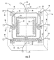
FIG. 2 illustrates a perspective view of a microelectromechanical systems die; -
FIG. 3 illustrates a perspective view of another microelectromechanical systems die; -
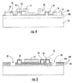
FIG. 4 illustrates a cross-sectional view of a microelectromechanical systems die; -
FIG. 5 illustrates a cross-sectional view of a microelectromechanical systems die; and -
FIG. 6 illustrates a cross-sectional view of an insulator stack. - For the purposes of promoting an understanding of the principles of the present disclosure, reference will now be made to the drawings, and specific language will be used to describe the same. It will nevertheless be understood that no limitation of the scope of this disclosure is thereby intended.
-
FIG. 1 illustrates a gas detector device, generally indicated at 10. Thegas detector device 10 includes a microelectromechanical systems (MEMS) die 12, andsensor material 14 disposed on the MEMS die 12. Thesensor material 14 is configured to detect the presence of a target gas as it passes over thesensor material 14. - With reference to
FIGs. 2 and3 , the MEMS die 12 includes a thermallyconductive substrate 16 and at least one insulator film 18 (shown inFIGs. 4-6 ) disposed over the thermallyconductive substrate 16. The thermallyconductive substrate 16 can be composed of silicon. Thesensing material 14 can be substantially centered on the at least oneinsulator film 18. - For example, the at least one
insulator film 18 includes two sets of twodifferent insulator films FIGs. 4-6 . The two sets of twoinsulator films insulator films - The MEMS die 12 includes at least one
electrode 22 in contact with thesensor material 14. In the Figures theelectrodes 22 are disposed around the periphery of thesensor material 14. For example, theelectrodes 22 may be in contact on opposing sides of thesensor material 14 in order to send an electrical signal across the sensing material from one side to an opposing side. It will be appreciated that the at least oneelectrode 22 may be composed of gold, or aluminum to name a couple of non-limiting examples - The MEMS die 12 further includes a
temperature sensor 24 disposed around thesensor material 14. Thetemperature sensor 24 is configured to monitor the temperature of thesensor material 14 in order to maintain aconstant sensor material 14 temperature in any environment. InFIG. 2 , thetemperature sensor 24 is circumferentially disposed around thesensor material 14. - It will be appreciated that the
temperature sensor 24 may be circumferential to, and/or underneath theelectrodes 22 andsensor material 14. It will be further appreciated that thetemperature sensor 24 may be disposed on or between any of the at least oneinsulator film 18, or on a bottom surface of the thermallyconductive substrate 16. It may be further appreciated that thetemperature sensor 24 may be enclosed by combinations of the at least oneinsulator film 18. Enclosing thetemperature sensor 24 may prevent electromigration or corrosion of thetemperature sensor 24 material. For example, enclosing thetemperature sensor material 24 with a silicon dioxide film may also prevent silicide formation. - In
FIG. 3 , thetemperature sensor 24 is shown surrounding three sides of thesensor material 14; thus, not crossing over the at least oneelectrode 22 orheater 26. It will be appreciated that thetemperature sensor 24 may be composed of platinum or nickel to name a couple of non-limiting examples and contain a corrosion prevention coating. - The MEMS die 12 further includes a
heater 26 circumferentially disposed around thesensor material 14, andtemperature sensor 24. Theheater 26 operates as a hot plate which controls the temperature of thesensor material 14 by applying a current through theheater 26. Theheater 26 can include a line width dimension, wherein the line width dimension is less than or equal to approximately 100 micrometers. It may also be appreciated that the line width of theheater 26 may be continuously varied to dissipate more or less power to heat theconductive substrate 16. It will also be appreciated that theheater 26 may be composed of platinum and nickel to name a couple of non-limiting examples, and contain a corrosion prevention coating. - There may be no cross-over between the
heater 26,temperature sensor 24 and the at least oneelectrode 22. For example, theheater 26 may be circumferential to, and/or underneath theelectrodes 22 andsensor material 14. Theheater 26 may also be disposed on or between any of the at least oneinsulator film 18, or a bottom surface of the thermallyconductive substrate 16. Theheater 26 may also be enclosed by combinations of the at least oneinsulator film 18. Enclosing theheater 26 may prevent electro-migration or corrosion of theheater 26 material. For example, enclosing theheater material 26 with a silicon dioxide film may prevent silicide formation. - The at least one
insulator film 18 may be deposited prior to formation of the at least oneelectrode 22,temperature sensor 24, andheater 26, and that the second set of insulator films may be deposited after the at least oneelectrode 22,temperature sensor 24, andheater 26 have been formed, so as to enclose portions of each of the at least oneelectrode 22,temperature sensor 24, andheater 26. - As shown in
FIGs. 1 ,2 ,3 and5 , the MEMS die 12 can include at least oneaperture 28 disposed within the at least oneinsulator film 18. The at least oneaperture 28 forms a contact point with the thermallyconductive substrate 16, is configured to provide an insulation resistance verification of the at least oneinsulator film 18, and allows for testing and diagnostics of the MEMS die 12. - It should be noted that barrier metals or other diffusion barriers, as are known in the art, may be employed to prevent substantial co-diffusion of the
temperature sensor 24 material into theheater 26 material where they contact each other, for example, in abond pad 32 or in the least oneaperture 28. Similarly, it should be noted that barrier metals or other diffusion barriers may be employed to prevent substantial co-diffusion of thetemperature sensor 24 material or theheater 26 material or both into the silicon substrate and vice versa. An appropriate barrier metal or other diffusion barrier may also be employed to prevent the material ofelectrode 22 from diffusing into thesensor material 14 where they are in contact. This may prevent undesirable shifts in the operating properties of thesensor material 14 over time, including stability, sensitivity or reaction time. - The MEMS die 12 may further include at least one
passive heat exchanger 30 operably coupled to at least onebond pad 32, the at least onebond pad 32 is disposed on the at least oneinsulator film surface 18. The at least onepassive heat exchanger 30 can be located on a periphery of the at least oneinsulator film surface 18. The at least onepassive heat exchanger 30 and the at least onebond pad 32 can be disposed within theaperture 28. It will be appreciated that the at least onepassive heat exchanger 30 may be coupled to the at least onebond pad 32 by any means known in the art, for example wire bonding, foil bonding, bump and flip chip to name a few non-limiting examples. - For example, the at least one
passive heat exchanger 30 may be a wire bond configured to provide a connection means of electrical input and output to at least theelectrode 22,detector 24,heater 26, andaperture 28. It will be appreciated that the at least onepassive heat exchanger 30 is part of a thermal isolation scheme to exchange heat between the MEMS die 12 and a gas detector package/environment, and include small diameters and long lengths to reduce the rate at which heat is transferred. It will be further appreciated that in the embodiment shown inFIG. 3 , theheater 26 substantially surroundsbond pads 32 such that there is no direct thermal path between thebond pads 32 and thesensor material 14. - The
passive heat exchangers 30 can be coupled to place the MEMS die 12 in a spider die (i.e. floating die) configuration; however, it will be appreciated that thesensor material 14 on the MEMS die 12 may be substantially thermally isolated from its mounting by a number of configurations, such as a membrane isolating a central heated mass, tethers isolating a central heated mass, a diaphragm or perforated diaphragm isolating a central mass, a cantilevered mounting, etc. to name a few non-limiting examples. It will further be appreciated that the MEMS die 12 may be mounted to a plastic, ceramic, or TO packages to name a few non-limiting examples. - It will be appreciated that the examples described herein include a MEMS die 12 including a
heater 26 circumferentially disposed around asensing material 14 to provide a more uniform heating to maximize the area available for detection. - While the invention has been illustrated and described in detail in the drawings and foregoing description, the same is to be considered as illustrative and not restrictive in character, it being understood that only certain embodiments have been shown and described and that all changes and modifications that come within the scope of the invention, as defined by the claims, are desired to be protected.
Claims (10)
- A microelectromechanical systems die comprising:a thermally conductive substrate;at least one insulator film disposed on the thermally conductive substrate;a sensor material disposed on the at least one insulator film; anda heater circumferentially disposed around the sensor material.
- The microelectromechanical systems die of claim 1, wherein the thermally conductive substrate is composed of silicon.
- The microelectromechanical systems die of claim 1 or 2, wherein the sensor material is substantially centered on the at least one insulator film.
- The microelectromechanical systems die of claim 1, 2 or 3, comprising:at least one bond pad disposed on the at least one insulator film; andat least one passive heat exchanger operably coupled to the at least one bond pad.
- The microelectromechanical systems die of claim 4, wherein the at least one passive heat exchanger is located on the periphery of the at least one insulator film.
- The microelectromechanical systems die of claim 4 or 5, wherein the at least one passive heat exchanger comprises wire bonds.
- The microelectromechanical systems die of any preceding claim, comprising a temperature sensor disposed around the sensor material and located between the heater and sensor material.
- The microelectromechanical systems die of any preceding claim, wherein the heater includes a line width dimension.
- The microelectromechanical systems die of claim 8, wherein the line width dimension is less than or equal to approximately 100 micrometers.
- A gas detector package comprising a microelectromechanical systems die as claimed in any preceding claim.
Applications Claiming Priority (1)
| Application Number | Priority Date | Filing Date | Title |
|---|---|---|---|
| US201562197924P | 2015-07-28 | 2015-07-28 |
Publications (2)
| Publication Number | Publication Date |
|---|---|
| EP3124963A1 true EP3124963A1 (en) | 2017-02-01 |
| EP3124963B1 EP3124963B1 (en) | 2022-06-08 |
Family
ID=56740843
Family Applications (1)
| Application Number | Title | Priority Date | Filing Date |
|---|---|---|---|
| EP16181663.2A Active EP3124963B1 (en) | 2015-07-28 | 2016-07-28 | Gas detector with a thermally uniform mems die |
Country Status (2)
| Country | Link |
|---|---|
| US (1) | US10273149B2 (en) |
| EP (1) | EP3124963B1 (en) |
Cited By (1)
| Publication number | Priority date | Publication date | Assignee | Title |
|---|---|---|---|---|
| US20170029270A1 (en) * | 2015-07-28 | 2017-02-02 | Carrier Corporation | Gas detector with a thermally uniform mems die |
Families Citing this family (2)
| Publication number | Priority date | Publication date | Assignee | Title |
|---|---|---|---|---|
| CA3034248A1 (en) | 2016-08-18 | 2018-02-22 | Carrier Corporation | Isolated sensor and method of isolating a sensor |
| CN113336184B (en) * | 2021-06-04 | 2023-12-19 | 微集电科技(苏州)有限公司 | MEMS infrared light source with closed membrane structure and preparation method thereof |
Citations (2)
| Publication number | Priority date | Publication date | Assignee | Title |
|---|---|---|---|---|
| US20110138882A1 (en) * | 2009-12-11 | 2011-06-16 | Electronics And Telecommunications Research Institute | Semiconductor gas sensor having low power consumption |
| WO2014012948A1 (en) * | 2012-07-16 | 2014-01-23 | Sgx Sensortech Sa | Micro-hotplate device and sensor comprising such micro-hotplate device |
Family Cites Families (14)
| Publication number | Priority date | Publication date | Assignee | Title |
|---|---|---|---|---|
| US6572830B1 (en) * | 1998-10-09 | 2003-06-03 | Motorola, Inc. | Integrated multilayered microfludic devices and methods for making the same |
| US6596236B2 (en) * | 1999-01-15 | 2003-07-22 | Advanced Technology Materials, Inc. | Micro-machined thin film sensor arrays for the detection of H2 containing gases, and method of making and using the same |
| US6399177B1 (en) * | 1999-06-03 | 2002-06-04 | The Penn State Research Foundation | Deposited thin film void-column network materials |
| US20040232535A1 (en) | 2003-05-22 | 2004-11-25 | Terry Tarn | Microelectromechanical device packages with integral heaters |
| US20070212263A1 (en) * | 2004-03-17 | 2007-09-13 | Nat. Inst. Of Adv. Industrial Sci. And Tech. | Micro Thermoelectric Type Gas Sensor |
| US20100239436A1 (en) * | 2005-05-17 | 2010-09-23 | Honeywell International Inc. | A thermal pump |
| US8736000B1 (en) | 2006-10-19 | 2014-05-27 | Sandia Corporation | Capacitive chemical sensor |
| JP2009058389A (en) | 2007-08-31 | 2009-03-19 | New Cosmos Electric Corp | Gas detection element |
| CN102132153B (en) | 2008-08-25 | 2014-08-20 | Nxp股份有限公司 | Reducing capacitive charging in electronic devices |
| JP5100733B2 (en) | 2009-10-05 | 2012-12-19 | 北陸電気工業株式会社 | Gas sensor element and manufacturing method thereof |
| US20120085750A1 (en) | 2010-10-08 | 2012-04-12 | Dyconex Ag | Covering Device for an Organic Substrate, Substrate with a Covering Device, and Method for Producing a Covering Device |
| CN103675048B (en) | 2013-11-18 | 2016-02-24 | 西安交通大学 | A kind of metal-oxide gas transducer based on MEMS and preparation technology |
| EP3124963B1 (en) * | 2015-07-28 | 2022-06-08 | Carrier Corporation | Gas detector with a thermally uniform mems die |
| ES2978368T3 (en) * | 2015-10-06 | 2024-09-11 | Carrier Corp | SMEM die with sensitive structures |
-
2016
- 2016-07-28 EP EP16181663.2A patent/EP3124963B1/en active Active
- 2016-07-28 US US15/222,754 patent/US10273149B2/en active Active
Patent Citations (2)
| Publication number | Priority date | Publication date | Assignee | Title |
|---|---|---|---|---|
| US20110138882A1 (en) * | 2009-12-11 | 2011-06-16 | Electronics And Telecommunications Research Institute | Semiconductor gas sensor having low power consumption |
| WO2014012948A1 (en) * | 2012-07-16 | 2014-01-23 | Sgx Sensortech Sa | Micro-hotplate device and sensor comprising such micro-hotplate device |
Non-Patent Citations (3)
| Title |
|---|
| BHATTACHARYYA P: "Technological Journey Towards Reliable Microheater Development for MEMS Gas Sensors: A Review", IEEE TRANSACTIONS ON DEVICE AND MATERIALS RELIABILITY, IEEE SERVICE CENTER, PISCATAWAY, NJ, US, vol. 14, no. 2, 1 June 2014 (2014-06-01), pages 589 - 599, XP011550087, ISSN: 1530-4388, [retrieved on 20140603], DOI: 10.1109/TDMR.2014.2311801 * |
| GREGOR WICHE: "Metalloxid-Gassensoren mit Siliziumcarbid Micro-Hotplate", 4 January 2008 (2008-01-04), XP055327829, Retrieved from the Internet <URL:https://depositonce.tu-berlin.de/bitstream/11303/2036/2/Dokument_50.pdf> [retrieved on 20161209] * |
| WICHE G ET AL: "Thermal analysis of silicon carbide based micro hotplates for metal oxide gas sensors", SENSORS AND ACTUATORS A: PHYSICAL, ELSEVIER BV, NL, vol. 123-124, 23 September 2005 (2005-09-23), pages 12 - 17, XP027807150, ISSN: 0924-4247, [retrieved on 20050923] * |
Cited By (2)
| Publication number | Priority date | Publication date | Assignee | Title |
|---|---|---|---|---|
| US20170029270A1 (en) * | 2015-07-28 | 2017-02-02 | Carrier Corporation | Gas detector with a thermally uniform mems die |
| US10273149B2 (en) * | 2015-07-28 | 2019-04-30 | Carrier Corporation | Gas detector with a thermally uniform MEMS die |
Also Published As
| Publication number | Publication date |
|---|---|
| US20170029270A1 (en) | 2017-02-02 |
| US10273149B2 (en) | 2019-04-30 |
| EP3124963B1 (en) | 2022-06-08 |
Similar Documents
| Publication | Publication Date | Title |
|---|---|---|
| JP6467173B2 (en) | Contact combustion type gas sensor | |
| US10823692B2 (en) | MEMS die with sensing structures | |
| JP2009529695A (en) | Thermal gas mass flow sensor and method of forming the same | |
| WO2006027974A1 (en) | Flow sensor | |
| KR101135404B1 (en) | Micro platform for gas sensor array | |
| US10273149B2 (en) | Gas detector with a thermally uniform MEMS die | |
| CN105209872A (en) | Thermopile differential scanning calorimeter sensor | |
| KR20100041708A (en) | Thermally insulating ceramic substrates for gas sensors | |
| CN106919203A (en) | Micro-electromechanical temperature control system with heat storage element | |
| CN115280113B (en) | Thermopile Sensors | |
| CN110729227A (en) | Vacuum chuck and apparatus for bonding substrates and method of bonding substrates | |
| JP2008089474A (en) | Sensor unit for thermal analysis equipment and method for manufacturing the same | |
| KR102219542B1 (en) | Contact combustion type gas sensor and method for manufacturing the same | |
| JP6355600B2 (en) | Sensor unit for thermal analyzer and thermal analyzer | |
| WO2016132934A1 (en) | Contact combustion-type gas sensor | |
| JPH01203957A (en) | Suspension structure for sensor device with temperature sensitive semiconductor device | |
| KR101746560B1 (en) | Multi-layered resistive-thermocouple type temperature measuring wafer sensor and method for fabricating the same | |
| KR100914938B1 (en) | Micro Heater, micro heater manufacturing method and environment sensor using thereof | |
| JP7631374B2 (en) | Temperature sensor assembly for vacuum device | |
| JP2012242227A (en) | Temperature detection wafer | |
| JP2022139173A (en) | flow sensor chip | |
| JP2016151472A (en) | Contact combustion type gas sensor | |
| EP4576930A1 (en) | Mems heater and mems fluid sensor | |
| JP2016151473A (en) | Thermal sensor | |
| WO2019111463A1 (en) | Humidity sensor and method for manufacturing same |
Legal Events
| Date | Code | Title | Description |
|---|---|---|---|
| PUAI | Public reference made under article 153(3) epc to a published international application that has entered the european phase |
Free format text: ORIGINAL CODE: 0009012 |
|
| STAA | Information on the status of an ep patent application or granted ep patent |
Free format text: STATUS: THE APPLICATION HAS BEEN PUBLISHED |
|
| AK | Designated contracting states |
Kind code of ref document: A1 Designated state(s): AL AT BE BG CH CY CZ DE DK EE ES FI FR GB GR HR HU IE IS IT LI LT LU LV MC MK MT NL NO PL PT RO RS SE SI SK SM TR |
|
| AX | Request for extension of the european patent |
Extension state: BA ME |
|
| STAA | Information on the status of an ep patent application or granted ep patent |
Free format text: STATUS: REQUEST FOR EXAMINATION WAS MADE |
|
| 17P | Request for examination filed |
Effective date: 20170728 |
|
| RBV | Designated contracting states (corrected) |
Designated state(s): AL AT BE BG CH CY CZ DE DK EE ES FI FR GB GR HR HU IE IS IT LI LT LU LV MC MK MT NL NO PL PT RO RS SE SI SK SM TR |
|
| RIN1 | Information on inventor provided before grant (corrected) |
Inventor name: CHRISTENSON, JOHN CARL Inventor name: POTASEK, DAVID P. Inventor name: CHILDRESS, MARCUS ALLEN |
|
| STAA | Information on the status of an ep patent application or granted ep patent |
Free format text: STATUS: EXAMINATION IS IN PROGRESS |
|
| 17Q | First examination report despatched |
Effective date: 20180817 |
|
| GRAP | Despatch of communication of intention to grant a patent |
Free format text: ORIGINAL CODE: EPIDOSNIGR1 |
|
| STAA | Information on the status of an ep patent application or granted ep patent |
Free format text: STATUS: GRANT OF PATENT IS INTENDED |
|
| INTG | Intention to grant announced |
Effective date: 20220214 |
|
| GRAS | Grant fee paid |
Free format text: ORIGINAL CODE: EPIDOSNIGR3 |
|
| GRAA | (expected) grant |
Free format text: ORIGINAL CODE: 0009210 |
|
| STAA | Information on the status of an ep patent application or granted ep patent |
Free format text: STATUS: THE PATENT HAS BEEN GRANTED |
|
| AK | Designated contracting states |
Kind code of ref document: B1 Designated state(s): AL AT BE BG CH CY CZ DE DK EE ES FI FR GB GR HR HU IE IS IT LI LT LU LV MC MK MT NL NO PL PT RO RS SE SI SK SM TR |
|
| REG | Reference to a national code |
Ref country code: GB Ref legal event code: FG4D |
|
| REG | Reference to a national code |
Ref country code: AT Ref legal event code: REF Ref document number: 1497264 Country of ref document: AT Kind code of ref document: T Effective date: 20220615 Ref country code: CH Ref legal event code: EP |
|
| REG | Reference to a national code |
Ref country code: DE Ref legal event code: R096 Ref document number: 602016072651 Country of ref document: DE |
|
| REG | Reference to a national code |
Ref country code: IE Ref legal event code: FG4D |
|
| REG | Reference to a national code |
Ref country code: NO Ref legal event code: T2 Effective date: 20220608 |
|
| REG | Reference to a national code |
Ref country code: LT Ref legal event code: MG9D |
|
| REG | Reference to a national code |
Ref country code: NL Ref legal event code: MP Effective date: 20220608 |
|
| PG25 | Lapsed in a contracting state [announced via postgrant information from national office to epo] |
Ref country code: SE Free format text: LAPSE BECAUSE OF FAILURE TO SUBMIT A TRANSLATION OF THE DESCRIPTION OR TO PAY THE FEE WITHIN THE PRESCRIBED TIME-LIMIT Effective date: 20220608 Ref country code: LT Free format text: LAPSE BECAUSE OF FAILURE TO SUBMIT A TRANSLATION OF THE DESCRIPTION OR TO PAY THE FEE WITHIN THE PRESCRIBED TIME-LIMIT Effective date: 20220608 Ref country code: HR Free format text: LAPSE BECAUSE OF FAILURE TO SUBMIT A TRANSLATION OF THE DESCRIPTION OR TO PAY THE FEE WITHIN THE PRESCRIBED TIME-LIMIT Effective date: 20220608 Ref country code: GR Free format text: LAPSE BECAUSE OF FAILURE TO SUBMIT A TRANSLATION OF THE DESCRIPTION OR TO PAY THE FEE WITHIN THE PRESCRIBED TIME-LIMIT Effective date: 20220909 Ref country code: FI Free format text: LAPSE BECAUSE OF FAILURE TO SUBMIT A TRANSLATION OF THE DESCRIPTION OR TO PAY THE FEE WITHIN THE PRESCRIBED TIME-LIMIT Effective date: 20220608 Ref country code: ES Free format text: LAPSE BECAUSE OF FAILURE TO SUBMIT A TRANSLATION OF THE DESCRIPTION OR TO PAY THE FEE WITHIN THE PRESCRIBED TIME-LIMIT Effective date: 20220608 Ref country code: BG Free format text: LAPSE BECAUSE OF FAILURE TO SUBMIT A TRANSLATION OF THE DESCRIPTION OR TO PAY THE FEE WITHIN THE PRESCRIBED TIME-LIMIT Effective date: 20220908 |
|
| REG | Reference to a national code |
Ref country code: AT Ref legal event code: MK05 Ref document number: 1497264 Country of ref document: AT Kind code of ref document: T Effective date: 20220608 |
|
| PG25 | Lapsed in a contracting state [announced via postgrant information from national office to epo] |
Ref country code: RS Free format text: LAPSE BECAUSE OF FAILURE TO SUBMIT A TRANSLATION OF THE DESCRIPTION OR TO PAY THE FEE WITHIN THE PRESCRIBED TIME-LIMIT Effective date: 20220608 Ref country code: LV Free format text: LAPSE BECAUSE OF FAILURE TO SUBMIT A TRANSLATION OF THE DESCRIPTION OR TO PAY THE FEE WITHIN THE PRESCRIBED TIME-LIMIT Effective date: 20220608 |
|
| PG25 | Lapsed in a contracting state [announced via postgrant information from national office to epo] |
Ref country code: NL Free format text: LAPSE BECAUSE OF FAILURE TO SUBMIT A TRANSLATION OF THE DESCRIPTION OR TO PAY THE FEE WITHIN THE PRESCRIBED TIME-LIMIT Effective date: 20220608 |
|
| PG25 | Lapsed in a contracting state [announced via postgrant information from national office to epo] |
Ref country code: SM Free format text: LAPSE BECAUSE OF FAILURE TO SUBMIT A TRANSLATION OF THE DESCRIPTION OR TO PAY THE FEE WITHIN THE PRESCRIBED TIME-LIMIT Effective date: 20220608 Ref country code: SK Free format text: LAPSE BECAUSE OF FAILURE TO SUBMIT A TRANSLATION OF THE DESCRIPTION OR TO PAY THE FEE WITHIN THE PRESCRIBED TIME-LIMIT Effective date: 20220608 Ref country code: RO Free format text: LAPSE BECAUSE OF FAILURE TO SUBMIT A TRANSLATION OF THE DESCRIPTION OR TO PAY THE FEE WITHIN THE PRESCRIBED TIME-LIMIT Effective date: 20220608 Ref country code: PT Free format text: LAPSE BECAUSE OF FAILURE TO SUBMIT A TRANSLATION OF THE DESCRIPTION OR TO PAY THE FEE WITHIN THE PRESCRIBED TIME-LIMIT Effective date: 20221010 Ref country code: EE Free format text: LAPSE BECAUSE OF FAILURE TO SUBMIT A TRANSLATION OF THE DESCRIPTION OR TO PAY THE FEE WITHIN THE PRESCRIBED TIME-LIMIT Effective date: 20220608 Ref country code: CZ Free format text: LAPSE BECAUSE OF FAILURE TO SUBMIT A TRANSLATION OF THE DESCRIPTION OR TO PAY THE FEE WITHIN THE PRESCRIBED TIME-LIMIT Effective date: 20220608 Ref country code: AT Free format text: LAPSE BECAUSE OF FAILURE TO SUBMIT A TRANSLATION OF THE DESCRIPTION OR TO PAY THE FEE WITHIN THE PRESCRIBED TIME-LIMIT Effective date: 20220608 |
|
| REG | Reference to a national code |
Ref country code: DE Ref legal event code: R119 Ref document number: 602016072651 Country of ref document: DE |
|
| PG25 | Lapsed in a contracting state [announced via postgrant information from national office to epo] |
Ref country code: PL Free format text: LAPSE BECAUSE OF FAILURE TO SUBMIT A TRANSLATION OF THE DESCRIPTION OR TO PAY THE FEE WITHIN THE PRESCRIBED TIME-LIMIT Effective date: 20220608 Ref country code: IS Free format text: LAPSE BECAUSE OF FAILURE TO SUBMIT A TRANSLATION OF THE DESCRIPTION OR TO PAY THE FEE WITHIN THE PRESCRIBED TIME-LIMIT Effective date: 20221008 |
|
| REG | Reference to a national code |
Ref country code: CH Ref legal event code: PL |
|
| REG | Reference to a national code |
Ref country code: BE Ref legal event code: MM Effective date: 20220731 |
|
| PG25 | Lapsed in a contracting state [announced via postgrant information from national office to epo] |
Ref country code: MC Free format text: LAPSE BECAUSE OF FAILURE TO SUBMIT A TRANSLATION OF THE DESCRIPTION OR TO PAY THE FEE WITHIN THE PRESCRIBED TIME-LIMIT Effective date: 20220608 Ref country code: AL Free format text: LAPSE BECAUSE OF FAILURE TO SUBMIT A TRANSLATION OF THE DESCRIPTION OR TO PAY THE FEE WITHIN THE PRESCRIBED TIME-LIMIT Effective date: 20220608 |
|
| PLBE | No opposition filed within time limit |
Free format text: ORIGINAL CODE: 0009261 |
|
| STAA | Information on the status of an ep patent application or granted ep patent |
Free format text: STATUS: NO OPPOSITION FILED WITHIN TIME LIMIT |
|
| PG25 | Lapsed in a contracting state [announced via postgrant information from national office to epo] |
Ref country code: LU Free format text: LAPSE BECAUSE OF NON-PAYMENT OF DUE FEES Effective date: 20220728 Ref country code: LI Free format text: LAPSE BECAUSE OF NON-PAYMENT OF DUE FEES Effective date: 20220731 Ref country code: DK Free format text: LAPSE BECAUSE OF FAILURE TO SUBMIT A TRANSLATION OF THE DESCRIPTION OR TO PAY THE FEE WITHIN THE PRESCRIBED TIME-LIMIT Effective date: 20220608 Ref country code: CH Free format text: LAPSE BECAUSE OF NON-PAYMENT OF DUE FEES Effective date: 20220731 |
|
| 26N | No opposition filed |
Effective date: 20230310 |
|
| PG25 | Lapsed in a contracting state [announced via postgrant information from national office to epo] |
Ref country code: SI Free format text: LAPSE BECAUSE OF FAILURE TO SUBMIT A TRANSLATION OF THE DESCRIPTION OR TO PAY THE FEE WITHIN THE PRESCRIBED TIME-LIMIT Effective date: 20220608 Ref country code: DE Free format text: LAPSE BECAUSE OF NON-PAYMENT OF DUE FEES Effective date: 20230201 Ref country code: BE Free format text: LAPSE BECAUSE OF NON-PAYMENT OF DUE FEES Effective date: 20220731 |
|
| PG25 | Lapsed in a contracting state [announced via postgrant information from national office to epo] |
Ref country code: IE Free format text: LAPSE BECAUSE OF NON-PAYMENT OF DUE FEES Effective date: 20220728 Ref country code: FR Free format text: LAPSE BECAUSE OF NON-PAYMENT OF DUE FEES Effective date: 20220808 |
|
| PG25 | Lapsed in a contracting state [announced via postgrant information from national office to epo] |
Ref country code: IT Free format text: LAPSE BECAUSE OF FAILURE TO SUBMIT A TRANSLATION OF THE DESCRIPTION OR TO PAY THE FEE WITHIN THE PRESCRIBED TIME-LIMIT Effective date: 20220608 |
|
| PG25 | Lapsed in a contracting state [announced via postgrant information from national office to epo] |
Ref country code: HU Free format text: LAPSE BECAUSE OF FAILURE TO SUBMIT A TRANSLATION OF THE DESCRIPTION OR TO PAY THE FEE WITHIN THE PRESCRIBED TIME-LIMIT; INVALID AB INITIO Effective date: 20160728 |
|
| PG25 | Lapsed in a contracting state [announced via postgrant information from national office to epo] |
Ref country code: MK Free format text: LAPSE BECAUSE OF FAILURE TO SUBMIT A TRANSLATION OF THE DESCRIPTION OR TO PAY THE FEE WITHIN THE PRESCRIBED TIME-LIMIT Effective date: 20220608 Ref country code: CY Free format text: LAPSE BECAUSE OF FAILURE TO SUBMIT A TRANSLATION OF THE DESCRIPTION OR TO PAY THE FEE WITHIN THE PRESCRIBED TIME-LIMIT Effective date: 20220608 |
|
| PG25 | Lapsed in a contracting state [announced via postgrant information from national office to epo] |
Ref country code: TR Free format text: LAPSE BECAUSE OF FAILURE TO SUBMIT A TRANSLATION OF THE DESCRIPTION OR TO PAY THE FEE WITHIN THE PRESCRIBED TIME-LIMIT Effective date: 20220608 |
|
| PG25 | Lapsed in a contracting state [announced via postgrant information from national office to epo] |
Ref country code: MT Free format text: LAPSE BECAUSE OF FAILURE TO SUBMIT A TRANSLATION OF THE DESCRIPTION OR TO PAY THE FEE WITHIN THE PRESCRIBED TIME-LIMIT Effective date: 20220608 |
|
| PG25 | Lapsed in a contracting state [announced via postgrant information from national office to epo] |
Ref country code: BG Free format text: LAPSE BECAUSE OF FAILURE TO SUBMIT A TRANSLATION OF THE DESCRIPTION OR TO PAY THE FEE WITHIN THE PRESCRIBED TIME-LIMIT Effective date: 20220608 |
|
| PG25 | Lapsed in a contracting state [announced via postgrant information from national office to epo] |
Ref country code: BG Free format text: LAPSE BECAUSE OF FAILURE TO SUBMIT A TRANSLATION OF THE DESCRIPTION OR TO PAY THE FEE WITHIN THE PRESCRIBED TIME-LIMIT Effective date: 20220608 |
|
| PGFP | Annual fee paid to national office [announced via postgrant information from national office to epo] |
Ref country code: GB Payment date: 20250619 Year of fee payment: 10 |
|
| PGFP | Annual fee paid to national office [announced via postgrant information from national office to epo] |
Ref country code: NO Payment date: 20250623 Year of fee payment: 10 |
|
| REG | Reference to a national code |
Ref country code: GB Ref legal event code: 732E Free format text: REGISTERED BETWEEN 20260305 AND 20260311 |