EP3121860A1 - Anordnung zur strombegrenzung in einem der stromversorgung dienenden netzwerk - Google Patents
Anordnung zur strombegrenzung in einem der stromversorgung dienenden netzwerk Download PDFInfo
- Publication number
- EP3121860A1 EP3121860A1 EP15306183.3A EP15306183A EP3121860A1 EP 3121860 A1 EP3121860 A1 EP 3121860A1 EP 15306183 A EP15306183 A EP 15306183A EP 3121860 A1 EP3121860 A1 EP 3121860A1
- Authority
- EP
- European Patent Office
- Prior art keywords
- phase
- phase conductors
- conductors
- network
- carrier
- Prior art date
- Legal status (The legal status is an assumption and is not a legal conclusion. Google has not performed a legal analysis and makes no representation as to the accuracy of the status listed.)
- Granted
Links
Images
Classifications
-
- H—ELECTRICITY
- H10—SEMICONDUCTOR DEVICES; ELECTRIC SOLID-STATE DEVICES NOT OTHERWISE PROVIDED FOR
- H10N—ELECTRIC SOLID-STATE DEVICES NOT OTHERWISE PROVIDED FOR
- H10N60/00—Superconducting devices
- H10N60/30—Devices switchable between superconducting and normal states
-
- H—ELECTRICITY
- H01—ELECTRIC ELEMENTS
- H01B—CABLES; CONDUCTORS; INSULATORS; SELECTION OF MATERIALS FOR THEIR CONDUCTIVE, INSULATING OR DIELECTRIC PROPERTIES
- H01B12/00—Superconductive or hyperconductive conductors, cables, or transmission lines
- H01B12/02—Superconductive or hyperconductive conductors, cables, or transmission lines characterised by their form
-
- H—ELECTRICITY
- H01—ELECTRIC ELEMENTS
- H01F—MAGNETS; INDUCTANCES; TRANSFORMERS; SELECTION OF MATERIALS FOR THEIR MAGNETIC PROPERTIES
- H01F6/00—Superconducting magnets; Superconducting coils
- H01F6/04—Cooling
-
- H—ELECTRICITY
- H01—ELECTRIC ELEMENTS
- H01B—CABLES; CONDUCTORS; INSULATORS; SELECTION OF MATERIALS FOR THEIR CONDUCTIVE, INSULATING OR DIELECTRIC PROPERTIES
- H01B12/00—Superconductive or hyperconductive conductors, cables, or transmission lines
- H01B12/14—Superconductive or hyperconductive conductors, cables, or transmission lines characterised by the disposition of thermal insulation
-
- H—ELECTRICITY
- H01—ELECTRIC ELEMENTS
- H01B—CABLES; CONDUCTORS; INSULATORS; SELECTION OF MATERIALS FOR THEIR CONDUCTIVE, INSULATING OR DIELECTRIC PROPERTIES
- H01B12/00—Superconductive or hyperconductive conductors, cables, or transmission lines
- H01B12/16—Superconductive or hyperconductive conductors, cables, or transmission lines characterised by cooling
-
- H—ELECTRICITY
- H01—ELECTRIC ELEMENTS
- H01F—MAGNETS; INDUCTANCES; TRANSFORMERS; SELECTION OF MATERIALS FOR THEIR MAGNETIC PROPERTIES
- H01F6/00—Superconducting magnets; Superconducting coils
- H01F6/06—Coils, e.g. winding, insulating, terminating or casing arrangements therefor
-
- H—ELECTRICITY
- H02—GENERATION; CONVERSION OR DISTRIBUTION OF ELECTRIC POWER
- H02H—EMERGENCY PROTECTIVE CIRCUIT ARRANGEMENTS
- H02H9/00—Emergency protective circuit arrangements for limiting excess current or voltage without disconnection
- H02H9/02—Emergency protective circuit arrangements for limiting excess current or voltage without disconnection responsive to excess current
- H02H9/023—Current limitation using superconducting elements
-
- Y—GENERAL TAGGING OF NEW TECHNOLOGICAL DEVELOPMENTS; GENERAL TAGGING OF CROSS-SECTIONAL TECHNOLOGIES SPANNING OVER SEVERAL SECTIONS OF THE IPC; TECHNICAL SUBJECTS COVERED BY FORMER USPC CROSS-REFERENCE ART COLLECTIONS [XRACs] AND DIGESTS
- Y02—TECHNOLOGIES OR APPLICATIONS FOR MITIGATION OR ADAPTATION AGAINST CLIMATE CHANGE
- Y02E—REDUCTION OF GREENHOUSE GAS [GHG] EMISSIONS, RELATED TO ENERGY GENERATION, TRANSMISSION OR DISTRIBUTION
- Y02E40/00—Technologies for an efficient electrical power generation, transmission or distribution
- Y02E40/60—Superconducting electric elements or equipment; Power systems integrating superconducting elements or equipment
Definitions
- the invention relates to a current limiting device in a power supply network which is integrated in the network and has superconductive conductors mounted on at least one plate-like carrier of insulating material.
- the known arrangements according to the above-mentioned documents have superconductive conductors which are arranged with a bifilar structure on disc-shaped carriers. Depending on the required conductor length, a suitable number of such carriers is arranged in a housing acting as a cryostat. For each phase of an alternating current network, such a cryostat is used in the assembly position.
- the preparation of the equipped with bifilar superconducting conductors carrier is expensive. Since a suitably constructed cryostat is used for each phase of the AC network, the space required for their construction is relatively large, especially if it is a three-phase AC network.
- the invention has for its object to simplify the above-described arrangement, both in construction and in handling.
- This object is achieved according to the invention in that on the at least one carrier three separate, arranged in spiral turns parallel to each other superconducting phase conductors for separate connection to the phases of a three-phase AC network are arranged.
- This arrangement can be connected as a compact, one-piece unit directly to a three-phase AC mains, via two electrical contact points for each phase conductor of the arrangement.
- the manufacture of the arrangement is relatively simple, because the three phase conductors thereof need only be arranged in spiral turns parallel to each other on the respective carrier. If necessary, they can simply be connected at their ends to phase conductors arranged on further carriers. For this purpose, simple connecting conductors are sufficient, which are connected between the ends of the phase conductors of a carrier and the beginnings of the phase conductors of another carrier.
- the arrangement can be installed independently of the number of carriers equipped with phase conductors in only one, designed as a cryostat container, which can be transported with little effort to the installation site and placed there with respect to the known arrangements reduced space requirements. Since all the required superconducting phase conductors are accommodated in only one cryostat, the overall arrangement requires less material for fixing the superconducting material.
- phase conductors of each carrier can be arranged with advantage voltage-resistant spacers, which preferably consist of glass fiber reinforced plastic.
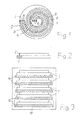
- phase conductors 2, 3 and 4 On a plate-like support 1 made of a mechanically stable plastic, such as glass fiber reinforced plastic, three superconducting phase conductors 2, 3 and 4 are arranged and fixed on the same.
- the phase conductors 2, 3 and 4 run in spiral turns parallel to each other. They are arranged on the surface of the carrier 1 so that it is substantially covered.
- contact elements 5 on the one hand and 6 on the other hand are advantageously mounted.
- phase conductors 2, 3 and 4 can be arranged as insulating medium according to the illustrated embodiment voltage-resistant spacers 7, 8 and 9, which are indicated by crosses and dashes and circles as different parts. They consist for example of glass fiber reinforced plastic. Each of the phase conductors 2, 3 and 4 may also be surrounded by electrical insulation material.
- Each phase conductor 2, 3 or 4 has a superconductive conductor, which can be advantageously designed as a band and can be arranged edgewise on the respective carrier 1.
- a superconductive conductor which can be advantageously designed as a band and can be arranged edgewise on the respective carrier 1.
- phase conductors 2, 3 and 4 can be used as an insulating medium, for example, a cooling medium, for example, liquid nitrogen, which is present in a cryostat, in the finished assembly within the at least one according to the preceding explanations stocked carrier 1 is used.
- a sufficient Number of arrangements according to the Fig. 1 and 2 electrically connected in series is advantageously a sufficient Number of arrangements according to the Fig. 1 and 2 electrically connected in series.
- This can be done according to arrangements Fig. 2
- Fig. 3 are in the container 10 five arrangements after Fig. 2 located, which are separated by spacers 11 from each other.
- Fig. 3 constructed container 10 or cryostat can be transported to the installation site and connected there to a three-phase AC power.
- the phase conductors 2, 3 and 4 are then cooled to a temperature at which the superconductive material changes to the superconducting state before being put into operation.
Landscapes
- Engineering & Computer Science (AREA)
- Power Engineering (AREA)
- Containers, Films, And Cooling For Superconductive Devices (AREA)
- Emergency Protection Circuit Devices (AREA)
Abstract
Description
- Die Erfindung bezieht sich auf eine Anordnung zur Strombegrenzung in einem der Stromversorgung dienenden Netzwerk, welche in dem Netzwerk integriert ist und supraleitfähige Leiter aufweist, die auf mindestens einem plattenartigen Träger aus Isoliermaterial angebracht sind.
- Eine solche Anordnung ist bekannt und beispielsweise in den Druckschriften
EP 0 503 448 A2 ,DE 10 2004 048 646 B4 undDE 10 2006 029 722 B3 beschrieben. Sie dient dazu, die Auswirkungen von Kurzschlüssen in der Stromversorgung dienenden Netzwerken zu vermeiden. Dabei werden die Eigenschaften von supraleitfähigen Materialien ausgenutzt, die bei ausreichend tiefen Temperaturen supraleitfähig werden und bei Überschreiten einer bestimmten Stromstärke, der kritischen Stromstärke, schlagartig in den normalleitenden Zustand übergehen. Der elektrische Gleichstromwiderstand eines supraleitfähigen Leiters ist bei ausreichender Kühlung Null, solange die kritische Stromstärke nicht überschritten wird. Geeignete Materialien sind beispielsweise oxidische Materialien auf Basis seltener Erden (ReBCO), insbesondere YBCO (Yttrium-Barium-Kupfer-Oxid) oder BSCCO (Wismut-Strontium-Kalzium-Kupfer-Oxid). Ausreichend niedrige Temperaturen, um ein derartiges Material in den supraleitfähigen Zustand zu bringen, liegen beispielsweise zwischen 67 K und 110 K. - Beim Auftreten eines Kurzschlussstromes wird die kritische Stromstärke eines supraleitfähigen Leiters überschritten, womit der Übergang vom supraleitfähigen Zustand, mit einem vernachlässigbar kleinen elektrischen Widerstand des Materials, in den normalleitenden Zustand, mit einem sehr hohen elektrischen Widerstand des Materials, einhergeht. Darüber hinaus erwärmt sich das Material im normalleitenden Zustand durch dessen ohmsche Verluste und der elektrische Widerstand steigt weiter an. Der Übergang des Materials vom supraleitenden in den normalleitenden Zustand geschieht beim Überschreiten der kritischen Stromstärke sehr schnell, typischerweise im Bereich von wenigen Millisekunden. Dadurch wird bei Einsatz einer der bekannten Anordnungen schnell ein elektrischer Widerstand in das Netzwerk eingeschaltet, welcher den Kurzschlussstrom begrenzt. Das Netzwerk und die Anordnung selbst werden dadurch gegenüber einem hohen Kurzschlussstrom geschützt.
- Die bekannten Anordnungen nach den im Vorangehenden erwähnten Druckschriften weisen supraleitfähige Leiter auf, die mit bifilarem Aufbau auf scheibenförmigen Trägern angeordnet sind. In Abhängigkeit von der benötigten Leiterlänge ist eine geeignete Anzahl solcher Träger in einem als Kryostat wirkenden Gehäuse angeordnet. Für jede Phase eines Wechselstromnetzes wird in Montageposition ein solcher Kryostat eingesetzt. Die Herstellung der mit bifilar angeordneten supraleitfähigen Leitern bestückten Träger ist aufwendig. Da für jede Phase des Wechselstromnetzes ein entsprechend aufgebauter Kryostat verwendet wird, ist der Platzbedarf für deren Aufbau relativ groß, insbesondere dann, wenn es sich um ein dreiphasiges Wechselstromnetz handelt.
- Der Erfindung liegt die Aufgabe zugrunde, die eingangs geschilderte Anordnung sowohl im Aufbau als auch in der Handhabung zu vereinfachen.
- Diese Aufgabe wird gemäß der Erfindung dadurch gelöst, daß auf dem mindestens einen Träger drei voneinander getrennte, in spiralförmigen Windungen parallel zueinander verlaufende supraleitfähige Phasenleiter zum getrennten Anschluß an die Phasen eines dreiphasigen Wechselstromnetzes angeordnet sind.
- Diese Anordnung ist als kompakte, einteilige Einheit direkt an ein dreiphasiges Wechselstrometz anschließbar, und zwar über zwei elektrische Kontaktstellen für jeden Phasenleiter der Anordnung. Die Fertigung der Anordnung ist relativ einfach, weil die drei Phasenleiter derselben nur in spiralförmigen Windungen parallel zueinander auf dem jeweiligen Träger angeordnet werden müssen. Sie können an ihren Enden gegebenenfalls einfach mit auf weiteren Trägern angeordneten Phasenleitern verbunden werden. Dazu reichen einfache Verbindungsleiter aus, die zwischen den Enden der Phasenleiter eines Trägers und den Anfängen der Phasenleiter eines weiteren Trägers angeschlossen werden. Die Anordnung kann unabhängig von der Anzahl der mit Phasenleitern bestückten Träger in nur einen, als Kryostat ausgebildeten Behälter eingebaut werden, der mit wenig Aufwand zum Montageort transportiert und dort mit gegenüber den bekannten Anordnungen vermindertem Platzbedarf aufgestellt werden kann. Da alle benötigten supraleitfähigen Phasenleiter in nur einem Kryostat untergebracht sind, wird für die Anordnung insgesamt weniger Material zur Fixierung des supraleitfähigen Materials benötigt.
- Zwischen den Phasenleitern jedes Trägers können mit Vorteil spannungsfeste Abstandshalter angeordnet sein, die vorzugsweise aus glasfaserverstärktem Kunststoff bestehen.
- Ein Ausführungsbeispiel des Erfindungsgegenstandes ist in den Zeichnungen dargestellt.
- Es zeigen:
-
Fig. 1 eine Draufsicht auf eine Anordnung nach der Erfindung in schematischer Darstellung. -
Fig. 2 eine Seitenansicht der Anordnung nachFig. 1 . -
Fig. 3 mehrere in einem Behälter angeordnete Anordnungen nachFig. 1 . - Auf einem plattenartigen Träger 1 aus einem mechanisch stabilen Kunststoff, wie beispielsweise glasfaserverstärkter Kunststoff, sind drei supraleitfähige Phasenleiter 2, 3 und 4 angeordnet und auf demselben befestigt. Die Phasenleiter 2, 3 und 4 verlaufen in spiralförmigen Windungen parallel zueinander. Sie sind auf der Oberfläche des Trägers 1 so angeordnet, daß dieselbe im Wesentlichen bedeckt ist. An den Enden der Phasenleiter 2, 3 und 4 sind mit Vorteil Kontaktelemente 5 einerseits und 6 andererseits angebracht.
- Zwischen den Windungen der Phasenleitern 2, 3 und 4 können als Isoliermedium entsprechend dem dargestellten Ausführungsbeispiel spannungsfeste Abstandshalter 7, 8 und 9 angeordnet sein, die durch Kreuze und Striche sowie Kreise als unterschiedliche Teile angedeutet sind. Sie bestehen beispielsweise aus glasfaserverstärktem Kunststoff. Jeder der Phasenleiter 2, 3 und 4 kann aber auch von elektrischem Isoliermaterial umgeben sein.
- Jeder Phasenleiter 2, 3 oder 4 weist einen supraleitfähigen Leiter auf, der mit Vorteil als Band ausgeführt und hochkant auf dem jeweiligen Träger 1 angeordnet sein kann. Dazu bietet sich beispielsweise für jeden Phasenleiter eine im Träger 1 angebrachte Nut an, die in den vorgesehenen spiralförmigen Windungen verläuft und in die der jeweilige Leiter eingreift. Das geht schematisch aus
Fig. 2 hervor. Bei derart auf dem jeweiligen Träger 1 fixierten Phasenleitern 2, 3 und 4 kann als Isoliermedium beispielsweise auch ein Kühlmedium, beispielsweise flüssiger Stickstoff, eingesetzt werden, das in einem Kryostat vorhanden ist, in den innerhalb der fertiggestellten Anordnung mindestens ein entsprechend den vorangehenden Erläuterungen bestückter Träger 1 eingesetzt ist. - Um eine für den jeweiligen Anwendungsfall ausreichende Länge der Phasenleiter 2, 3 und 4 zu erhalten, wird mit Vorteil eine ausreichende Anzahl von Anordnungen nach den
Fig. 1 und 2 elektrisch in Reihe geschaltet. Dazu können Anordnungen nachFig. 2 beispielsweise übereinander liegend in einem Behälter 10 angeordnet werden, welcher vakuumisoliert und damit als Kryostat ausgeführt ist. InFig. 3 sind in dem Behälter 10 fünf Anordnungen nachFig. 2 eingezeichnet, die durch Zwischenlagen 11 voneinander getrennt sind. - Ein beispielsweise nach
Fig. 3 aufgebauter Behälter 10 bzw. Kryostat kann zum Montageort transportiert und dort an ein dreiphasiges Wechselstromnetz angeschlossen werden. Die Phasenleiter 2, 3 und 4 werden dann vor Inbetriebnahme auf eine Temperatur abgekühlt, bei der das supraleitfähige Material in den supraleitfähigen Zustand übergeht.
Claims (4)
- Anordnung zur Strombegrenzung in einem der Stromversorgung dienenden Netzwerk, welche in dem Netzwerk integriert ist und supraleitfähige Leiter aufweist, die auf mindestens einem plattenartigen Träger aus Isoliermaterial angebracht sind, dadurch gekennzeichnet, daß auf dem mindestens einen Träger (1) drei voneinander getrennte, in spiralförmigen Windungen parallel zueinander verlaufende supraleitfähige Phasenleiter (2,3,4) zum getrennten Anschluß an die Phasen eines dreiphasigen Wechselstromnetzes angeordnet sind.
- Anordnung nach Anspruch 1, dadurch gekennzeichnet, daß zwischen den drei Phasenleitern (2,3,4) jeweils spannungsfeste Abstandshalter (7,8,9) angebracht sind.
- Anordnung nach Anspruch 1, dadurch gekennzeichnet,- daß die Phasenleiter (2,3,4) mit ihren spiralförmigen Windungen auf dem mindestens einen Träger (1) fixiert sind und- daß ein Kühlmedium, vorzugsweise flüssiger Stickstoff, als Isoliermedium zwischen den Phasenleitern (2,3,4) angeordnet ist.
- Anordnung nach Anspruch 1, dadurch gekennzeichnet, daß jeder der Phasenleiter (2,3,4) von elektrischem Isoliermaterial umgeben ist.
Priority Applications (3)
| Application Number | Priority Date | Filing Date | Title |
|---|---|---|---|
| EP15306183.3A EP3121860B1 (de) | 2015-07-21 | 2015-07-21 | Anordnung zur strombegrenzung in einem der stromversorgung dienenden netzwerk |
| US15/213,882 US10332664B2 (en) | 2015-07-21 | 2016-07-19 | Arrangement for current limitation which is suitable for integration into a power supply serving network |
| KR1020160092654A KR102571959B1 (ko) | 2015-07-21 | 2016-07-21 | 전력 공급 서비스 네트워크에 통합될 수 있는 전류 제한 장치 |
Applications Claiming Priority (1)
| Application Number | Priority Date | Filing Date | Title |
|---|---|---|---|
| EP15306183.3A EP3121860B1 (de) | 2015-07-21 | 2015-07-21 | Anordnung zur strombegrenzung in einem der stromversorgung dienenden netzwerk |
Publications (2)
| Publication Number | Publication Date |
|---|---|
| EP3121860A1 true EP3121860A1 (de) | 2017-01-25 |
| EP3121860B1 EP3121860B1 (de) | 2020-11-25 |
Family
ID=53758157
Family Applications (1)
| Application Number | Title | Priority Date | Filing Date |
|---|---|---|---|
| EP15306183.3A Not-in-force EP3121860B1 (de) | 2015-07-21 | 2015-07-21 | Anordnung zur strombegrenzung in einem der stromversorgung dienenden netzwerk |
Country Status (3)
| Country | Link |
|---|---|
| US (1) | US10332664B2 (de) |
| EP (1) | EP3121860B1 (de) |
| KR (1) | KR102571959B1 (de) |
Families Citing this family (3)
| Publication number | Priority date | Publication date | Assignee | Title |
|---|---|---|---|---|
| CN108899157B (zh) * | 2018-08-17 | 2024-02-13 | 广东电网有限责任公司 | 一种螺旋结构的限流器超导线圈 |
| WO2020162993A1 (en) | 2018-10-27 | 2020-08-13 | PsiQuantum Corp. | Superconductor switch |
| CN111243822A (zh) * | 2020-03-23 | 2020-06-05 | 北京交通大学 | 一种超导限流器并联带材的支撑结构 |
Citations (8)
| Publication number | Priority date | Publication date | Assignee | Title |
|---|---|---|---|---|
| DD110985A1 (de) * | 1973-12-20 | 1975-01-12 | ||
| EP0503448A2 (de) | 1991-03-09 | 1992-09-16 | ABBPATENT GmbH | Verfahren zur Herstellung eines supraleitenden Strombegrenzers sowie ein entsprechend hergestellter Strombegrenzer |
| WO1999033122A1 (de) * | 1997-12-19 | 1999-07-01 | Siemens Aktiengesellschaft | SUPRALEITERAUFBAU MIT HOCH-Tc-SUPRALEITERMATERIAL, VERFAHREN ZUR HERSTELLUNG DES AUFBAUS SOWIE STROMBEGRENZEREINRICHTUNG MIT EINEM SOLCHEN AUFBAU |
| DE19832274A1 (de) * | 1998-07-17 | 2000-01-20 | Siemens Ag | Resistiver Kurzschlußstrombegrenzer mit einer Leiterbahnstruktur aus Hoch-T¶c¶-Supraleitermaterial sowie Verfahren zur Herstellung des Strombegrenzers |
| DE102004048646B4 (de) | 2004-10-04 | 2006-08-10 | Siemens Ag | Supraleitende Strombegrenzereinrichtung vom resistiven Typ mit bandförmiger Hoch-Tc-Supraleiterbahn |
| DE102008029722B3 (de) | 2008-06-23 | 2009-12-17 | Siemens Aktiengesellschaft | Leiteranordnung für ein resistives Schaltelement mit wenigstens zwei Leiterverbünden aus supraleitenden Leiterbändern |
| US20130255991A1 (en) * | 2012-03-30 | 2013-10-03 | American Superconductor Corporation | Reduced-loss bucking bundle low voltage cable |
| WO2014126006A1 (ja) * | 2013-02-13 | 2014-08-21 | 古河電気工業株式会社 | 超電導限流器及び超電導限流器内の超電導素子の冷却方法 |
Family Cites Families (10)
| Publication number | Priority date | Publication date | Assignee | Title |
|---|---|---|---|---|
| DE110985T1 (de) | 1982-06-07 | 1985-01-31 | Ncr Corp., Dayton, Ohio | Tintenstrahldrucker. |
| FR2701157B1 (fr) * | 1993-02-04 | 1995-03-31 | Alsthom Cge Alcatel | Liaison d'alimentation pour bobine supraconductrice. |
| JPH06303797A (ja) * | 1993-04-12 | 1994-10-28 | Nippon Steel Corp | 超電導リニア誘導モータ駆動装置 |
| US7019608B2 (en) * | 2000-03-21 | 2006-03-28 | Metal Manufactures Limited | Superconducting transformer |
| US8037695B2 (en) * | 2003-07-04 | 2011-10-18 | Rolls-Royce Plc | Fault current limiter |
| KR100505054B1 (ko) * | 2003-09-30 | 2005-08-02 | 엘에스산전 주식회사 | 초전도 저항형 한류기 |
| US7629860B2 (en) * | 2007-06-08 | 2009-12-08 | Stats Chippac, Ltd. | Miniaturized wide-band baluns for RF applications |
| GB2466414B (en) * | 2007-11-01 | 2012-10-17 | Zenergy Power Pty Ltd | High voltage saturated core fault current limiter |
| EP2228806B1 (de) * | 2009-03-13 | 2011-08-03 | Nexans | Anordnung zur Strombegrenzung |
| JP6117126B2 (ja) * | 2013-02-13 | 2017-04-19 | 古河電気工業株式会社 | 超電導限流器及び超電導限流器内の超電導素子の冷却方法 |
-
2015
- 2015-07-21 EP EP15306183.3A patent/EP3121860B1/de not_active Not-in-force
-
2016
- 2016-07-19 US US15/213,882 patent/US10332664B2/en not_active Expired - Fee Related
- 2016-07-21 KR KR1020160092654A patent/KR102571959B1/ko active Active
Patent Citations (9)
| Publication number | Priority date | Publication date | Assignee | Title |
|---|---|---|---|---|
| DD110985A1 (de) * | 1973-12-20 | 1975-01-12 | ||
| EP0503448A2 (de) | 1991-03-09 | 1992-09-16 | ABBPATENT GmbH | Verfahren zur Herstellung eines supraleitenden Strombegrenzers sowie ein entsprechend hergestellter Strombegrenzer |
| WO1999033122A1 (de) * | 1997-12-19 | 1999-07-01 | Siemens Aktiengesellschaft | SUPRALEITERAUFBAU MIT HOCH-Tc-SUPRALEITERMATERIAL, VERFAHREN ZUR HERSTELLUNG DES AUFBAUS SOWIE STROMBEGRENZEREINRICHTUNG MIT EINEM SOLCHEN AUFBAU |
| DE19832274A1 (de) * | 1998-07-17 | 2000-01-20 | Siemens Ag | Resistiver Kurzschlußstrombegrenzer mit einer Leiterbahnstruktur aus Hoch-T¶c¶-Supraleitermaterial sowie Verfahren zur Herstellung des Strombegrenzers |
| DE102004048646B4 (de) | 2004-10-04 | 2006-08-10 | Siemens Ag | Supraleitende Strombegrenzereinrichtung vom resistiven Typ mit bandförmiger Hoch-Tc-Supraleiterbahn |
| DE102008029722B3 (de) | 2008-06-23 | 2009-12-17 | Siemens Aktiengesellschaft | Leiteranordnung für ein resistives Schaltelement mit wenigstens zwei Leiterverbünden aus supraleitenden Leiterbändern |
| US20130255991A1 (en) * | 2012-03-30 | 2013-10-03 | American Superconductor Corporation | Reduced-loss bucking bundle low voltage cable |
| WO2014126006A1 (ja) * | 2013-02-13 | 2014-08-21 | 古河電気工業株式会社 | 超電導限流器及び超電導限流器内の超電導素子の冷却方法 |
| EP2945199A1 (de) * | 2013-02-13 | 2015-11-18 | Furukawa Electric Co., Ltd. | Supraleitender fehlerstrombegrenzer und kühlverfahren für ein supraleitendes element in dem supraleitenden fehlerstrombegrenzer |
Also Published As
| Publication number | Publication date |
|---|---|
| EP3121860B1 (de) | 2020-11-25 |
| KR20170012101A (ko) | 2017-02-02 |
| KR102571959B1 (ko) | 2023-08-29 |
| US10332664B2 (en) | 2019-06-25 |
| US20170025209A1 (en) | 2017-01-26 |
Similar Documents
| Publication | Publication Date | Title |
|---|---|---|
| EP2228806B1 (de) | Anordnung zur Strombegrenzung | |
| EP2289077B1 (de) | Leiteranordnung für ein resistives schaltelement mit wenigstens zwei leiterverbünden aus supraleitenden leiterbändern | |
| EP2387043A1 (de) | Übertragungssystem mit einem supraleitfähigen Kabel | |
| EP2418747B1 (de) | Anordnung zum elektrisch leitenden Verbinden von zwei elektrischen Einheiten | |
| EP2284845B1 (de) | HTSL-Stromzuleitung zur Verbindung eines supraleitenden Verbrauchersystems mit einem Stromeinspeisepunkt | |
| DE102012217990A1 (de) | Supraleitende Spuleneinrichtung und Herstellungsverfahren | |
| EP2901460A1 (de) | Magnetspulenanordnung umfassend einen htsl-bandleiter und einen lts-draht, die einen joint ausbilden | |
| WO1999066566A1 (de) | STROMBEGRENZUNGSEINRICHTUNG MIT LEITERBAHNANORDNUNG AUS HOCH-Tc-SUPRALEITERMATERIAL SOWIE VERFAHREN ZUR HERSTELLUNG DER EINRICHTUNG | |
| EP2071589B1 (de) | Supraleitfähiges elektrisches Kabel | |
| DE3405310A1 (de) | Supraleitendes magnetsystem fuer den betrieb bei 13k | |
| EP2369600A1 (de) | Supraleitfähiges elektrisches Gleichstrom-Kabel | |
| EP2634779B1 (de) | System mit einem dreiphasigen supraleitfähigen elektrischen Übertragungselement | |
| EP3121860B1 (de) | Anordnung zur strombegrenzung in einem der stromversorgung dienenden netzwerk | |
| EP2041808B1 (de) | Supraleitende strombegrenzereinrichtung vom resistiven typ mit halteelement | |
| EP2551859B1 (de) | Anordnung mit einem supraleitfähigen elektrischen Gleichstrom-Kabelsystem | |
| EP2339593A1 (de) | Supraleitfähiges Kabelsystem | |
| EP2770514A1 (de) | Verfahren zum Kühlen eines supraleitfähigen Kabels | |
| EP2209129B1 (de) | Anordnung zur Strombegrenzung | |
| WO2004006345A2 (de) | Bifilare bandleiterstruktur eines hochtemperatursupraleiters zur strombegrenzung | |
| DE102018213598A1 (de) | Supraleitende Stromzuführung | |
| DE19832273C1 (de) | Resistiver Strombegrenzer mit Hoch-T¶c¶-Supraleitermaterial sowie Verfahren zur Herstellung des Strombegrenzers | |
| DE10163008C5 (de) | Resistive Strombegrenzungseinrichtung mit mindestens einer Leiterbahn mit supraleitendem und normalleitendem Material | |
| DE102015114208A1 (de) | Transformator, Wickelkörper dafür und Verfahren zur Herstellung eines Wickelkörpers | |
| EP3861573B1 (de) | Supraleitende strombegrenzereinrichtung mit stromzuführung | |
| DE10003725C2 (de) | Resistive Strombegrenzungseinrichtung mit Hoch-T¶c¶-Supraleitermaterial sowie Verfahren zur Herstellung und Verwendung der Einrichtung |
Legal Events
| Date | Code | Title | Description |
|---|---|---|---|
| PUAI | Public reference made under article 153(3) epc to a published international application that has entered the european phase |
Free format text: ORIGINAL CODE: 0009012 |
|
| STAA | Information on the status of an ep patent application or granted ep patent |
Free format text: STATUS: REQUEST FOR EXAMINATION WAS MADE |
|
| 17P | Request for examination filed |
Effective date: 20160216 |
|
| AK | Designated contracting states |
Kind code of ref document: A1 Designated state(s): AL AT BE BG CH CY CZ DE DK EE ES FI FR GB GR HR HU IE IS IT LI LT LU LV MC MK MT NL NO PL PT RO RS SE SI SK SM TR |
|
| AX | Request for extension of the european patent |
Extension state: BA ME |
|
| RAP1 | Party data changed (applicant data changed or rights of an application transferred) |
Owner name: NEXANS |
|
| STAA | Information on the status of an ep patent application or granted ep patent |
Free format text: STATUS: EXAMINATION IS IN PROGRESS |
|
| 17Q | First examination report despatched |
Effective date: 20171016 |
|
| GRAP | Despatch of communication of intention to grant a patent |
Free format text: ORIGINAL CODE: EPIDOSNIGR1 |
|
| STAA | Information on the status of an ep patent application or granted ep patent |
Free format text: STATUS: GRANT OF PATENT IS INTENDED |
|
| INTG | Intention to grant announced |
Effective date: 20200618 |
|
| GRAS | Grant fee paid |
Free format text: ORIGINAL CODE: EPIDOSNIGR3 |
|
| GRAA | (expected) grant |
Free format text: ORIGINAL CODE: 0009210 |
|
| STAA | Information on the status of an ep patent application or granted ep patent |
Free format text: STATUS: THE PATENT HAS BEEN GRANTED |
|
| AK | Designated contracting states |
Kind code of ref document: B1 Designated state(s): AL AT BE BG CH CY CZ DE DK EE ES FI FR GB GR HR HU IE IS IT LI LT LU LV MC MK MT NL NO PL PT RO RS SE SI SK SM TR |
|
| REG | Reference to a national code |
Ref country code: GB Ref legal event code: FG4D Free format text: NOT ENGLISH |
|
| REG | Reference to a national code |
Ref country code: CH Ref legal event code: EP |
|
| REG | Reference to a national code |
Ref country code: AT Ref legal event code: REF Ref document number: 1339299 Country of ref document: AT Kind code of ref document: T Effective date: 20201215 |
|
| REG | Reference to a national code |
Ref country code: DE Ref legal event code: R096 Ref document number: 502015013888 Country of ref document: DE |
|
| REG | Reference to a national code |
Ref country code: IE Ref legal event code: FG4D Free format text: LANGUAGE OF EP DOCUMENT: GERMAN |
|
| REG | Reference to a national code |
Ref country code: NL Ref legal event code: MP Effective date: 20201125 |
|
| PG25 | Lapsed in a contracting state [announced via postgrant information from national office to epo] |
Ref country code: GR Free format text: LAPSE BECAUSE OF FAILURE TO SUBMIT A TRANSLATION OF THE DESCRIPTION OR TO PAY THE FEE WITHIN THE PRESCRIBED TIME-LIMIT Effective date: 20210226 Ref country code: PT Free format text: LAPSE BECAUSE OF FAILURE TO SUBMIT A TRANSLATION OF THE DESCRIPTION OR TO PAY THE FEE WITHIN THE PRESCRIBED TIME-LIMIT Effective date: 20210325 Ref country code: NO Free format text: LAPSE BECAUSE OF FAILURE TO SUBMIT A TRANSLATION OF THE DESCRIPTION OR TO PAY THE FEE WITHIN THE PRESCRIBED TIME-LIMIT Effective date: 20210225 Ref country code: FI Free format text: LAPSE BECAUSE OF FAILURE TO SUBMIT A TRANSLATION OF THE DESCRIPTION OR TO PAY THE FEE WITHIN THE PRESCRIBED TIME-LIMIT Effective date: 20201125 Ref country code: RS Free format text: LAPSE BECAUSE OF FAILURE TO SUBMIT A TRANSLATION OF THE DESCRIPTION OR TO PAY THE FEE WITHIN THE PRESCRIBED TIME-LIMIT Effective date: 20201125 |
|
| PG25 | Lapsed in a contracting state [announced via postgrant information from national office to epo] |
Ref country code: BG Free format text: LAPSE BECAUSE OF FAILURE TO SUBMIT A TRANSLATION OF THE DESCRIPTION OR TO PAY THE FEE WITHIN THE PRESCRIBED TIME-LIMIT Effective date: 20210225 Ref country code: LV Free format text: LAPSE BECAUSE OF FAILURE TO SUBMIT A TRANSLATION OF THE DESCRIPTION OR TO PAY THE FEE WITHIN THE PRESCRIBED TIME-LIMIT Effective date: 20201125 Ref country code: IS Free format text: LAPSE BECAUSE OF FAILURE TO SUBMIT A TRANSLATION OF THE DESCRIPTION OR TO PAY THE FEE WITHIN THE PRESCRIBED TIME-LIMIT Effective date: 20210325 Ref country code: SE Free format text: LAPSE BECAUSE OF FAILURE TO SUBMIT A TRANSLATION OF THE DESCRIPTION OR TO PAY THE FEE WITHIN THE PRESCRIBED TIME-LIMIT Effective date: 20201125 Ref country code: PL Free format text: LAPSE BECAUSE OF FAILURE TO SUBMIT A TRANSLATION OF THE DESCRIPTION OR TO PAY THE FEE WITHIN THE PRESCRIBED TIME-LIMIT Effective date: 20201125 |
|
| REG | Reference to a national code |
Ref country code: LT Ref legal event code: MG9D |
|
| PG25 | Lapsed in a contracting state [announced via postgrant information from national office to epo] |
Ref country code: HR Free format text: LAPSE BECAUSE OF FAILURE TO SUBMIT A TRANSLATION OF THE DESCRIPTION OR TO PAY THE FEE WITHIN THE PRESCRIBED TIME-LIMIT Effective date: 20201125 |
|
| PG25 | Lapsed in a contracting state [announced via postgrant information from national office to epo] |
Ref country code: CZ Free format text: LAPSE BECAUSE OF FAILURE TO SUBMIT A TRANSLATION OF THE DESCRIPTION OR TO PAY THE FEE WITHIN THE PRESCRIBED TIME-LIMIT Effective date: 20201125 Ref country code: EE Free format text: LAPSE BECAUSE OF FAILURE TO SUBMIT A TRANSLATION OF THE DESCRIPTION OR TO PAY THE FEE WITHIN THE PRESCRIBED TIME-LIMIT Effective date: 20201125 Ref country code: SM Free format text: LAPSE BECAUSE OF FAILURE TO SUBMIT A TRANSLATION OF THE DESCRIPTION OR TO PAY THE FEE WITHIN THE PRESCRIBED TIME-LIMIT Effective date: 20201125 Ref country code: LT Free format text: LAPSE BECAUSE OF FAILURE TO SUBMIT A TRANSLATION OF THE DESCRIPTION OR TO PAY THE FEE WITHIN THE PRESCRIBED TIME-LIMIT Effective date: 20201125 Ref country code: SK Free format text: LAPSE BECAUSE OF FAILURE TO SUBMIT A TRANSLATION OF THE DESCRIPTION OR TO PAY THE FEE WITHIN THE PRESCRIBED TIME-LIMIT Effective date: 20201125 Ref country code: RO Free format text: LAPSE BECAUSE OF FAILURE TO SUBMIT A TRANSLATION OF THE DESCRIPTION OR TO PAY THE FEE WITHIN THE PRESCRIBED TIME-LIMIT Effective date: 20201125 |
|
| REG | Reference to a national code |
Ref country code: DE Ref legal event code: R097 Ref document number: 502015013888 Country of ref document: DE |
|
| PG25 | Lapsed in a contracting state [announced via postgrant information from national office to epo] |
Ref country code: DK Free format text: LAPSE BECAUSE OF FAILURE TO SUBMIT A TRANSLATION OF THE DESCRIPTION OR TO PAY THE FEE WITHIN THE PRESCRIBED TIME-LIMIT Effective date: 20201125 |
|
| PLBE | No opposition filed within time limit |
Free format text: ORIGINAL CODE: 0009261 |
|
| STAA | Information on the status of an ep patent application or granted ep patent |
Free format text: STATUS: NO OPPOSITION FILED WITHIN TIME LIMIT |
|
| PG25 | Lapsed in a contracting state [announced via postgrant information from national office to epo] |
Ref country code: NL Free format text: LAPSE BECAUSE OF FAILURE TO SUBMIT A TRANSLATION OF THE DESCRIPTION OR TO PAY THE FEE WITHIN THE PRESCRIBED TIME-LIMIT Effective date: 20201125 Ref country code: AL Free format text: LAPSE BECAUSE OF FAILURE TO SUBMIT A TRANSLATION OF THE DESCRIPTION OR TO PAY THE FEE WITHIN THE PRESCRIBED TIME-LIMIT Effective date: 20201125 Ref country code: IT Free format text: LAPSE BECAUSE OF FAILURE TO SUBMIT A TRANSLATION OF THE DESCRIPTION OR TO PAY THE FEE WITHIN THE PRESCRIBED TIME-LIMIT Effective date: 20201125 |
|
| 26N | No opposition filed |
Effective date: 20210826 |
|
| PG25 | Lapsed in a contracting state [announced via postgrant information from national office to epo] |
Ref country code: ES Free format text: LAPSE BECAUSE OF FAILURE TO SUBMIT A TRANSLATION OF THE DESCRIPTION OR TO PAY THE FEE WITHIN THE PRESCRIBED TIME-LIMIT Effective date: 20201125 Ref country code: SI Free format text: LAPSE BECAUSE OF FAILURE TO SUBMIT A TRANSLATION OF THE DESCRIPTION OR TO PAY THE FEE WITHIN THE PRESCRIBED TIME-LIMIT Effective date: 20201125 |
|
| REG | Reference to a national code |
Ref country code: CH Ref legal event code: PL |
|
| PG25 | Lapsed in a contracting state [announced via postgrant information from national office to epo] |
Ref country code: MC Free format text: LAPSE BECAUSE OF FAILURE TO SUBMIT A TRANSLATION OF THE DESCRIPTION OR TO PAY THE FEE WITHIN THE PRESCRIBED TIME-LIMIT Effective date: 20201125 |
|
| REG | Reference to a national code |
Ref country code: BE Ref legal event code: MM Effective date: 20210731 |
|
| PG25 | Lapsed in a contracting state [announced via postgrant information from national office to epo] |
Ref country code: LI Free format text: LAPSE BECAUSE OF NON-PAYMENT OF DUE FEES Effective date: 20210731 Ref country code: CH Free format text: LAPSE BECAUSE OF NON-PAYMENT OF DUE FEES Effective date: 20210731 |
|
| PG25 | Lapsed in a contracting state [announced via postgrant information from national office to epo] |
Ref country code: IS Free format text: LAPSE BECAUSE OF FAILURE TO SUBMIT A TRANSLATION OF THE DESCRIPTION OR TO PAY THE FEE WITHIN THE PRESCRIBED TIME-LIMIT Effective date: 20210325 Ref country code: LU Free format text: LAPSE BECAUSE OF NON-PAYMENT OF DUE FEES Effective date: 20210721 |
|
| PG25 | Lapsed in a contracting state [announced via postgrant information from national office to epo] |
Ref country code: IE Free format text: LAPSE BECAUSE OF NON-PAYMENT OF DUE FEES Effective date: 20210721 Ref country code: BE Free format text: LAPSE BECAUSE OF NON-PAYMENT OF DUE FEES Effective date: 20210731 |
|
| REG | Reference to a national code |
Ref country code: AT Ref legal event code: MM01 Ref document number: 1339299 Country of ref document: AT Kind code of ref document: T Effective date: 20210721 |
|
| PG25 | Lapsed in a contracting state [announced via postgrant information from national office to epo] |
Ref country code: AT Free format text: LAPSE BECAUSE OF NON-PAYMENT OF DUE FEES Effective date: 20210721 |
|
| REG | Reference to a national code |
Ref country code: DE Ref legal event code: R079 Ref document number: 502015013888 Country of ref document: DE Free format text: PREVIOUS MAIN CLASS: H01L0039160000 Ipc: H10N0060300000 |
|
| PG25 | Lapsed in a contracting state [announced via postgrant information from national office to epo] |
Ref country code: HU Free format text: LAPSE BECAUSE OF FAILURE TO SUBMIT A TRANSLATION OF THE DESCRIPTION OR TO PAY THE FEE WITHIN THE PRESCRIBED TIME-LIMIT; INVALID AB INITIO Effective date: 20150721 |
|
| PG25 | Lapsed in a contracting state [announced via postgrant information from national office to epo] |
Ref country code: CY Free format text: LAPSE BECAUSE OF FAILURE TO SUBMIT A TRANSLATION OF THE DESCRIPTION OR TO PAY THE FEE WITHIN THE PRESCRIBED TIME-LIMIT Effective date: 20201125 |
|
| PG25 | Lapsed in a contracting state [announced via postgrant information from national office to epo] |
Ref country code: MK Free format text: LAPSE BECAUSE OF FAILURE TO SUBMIT A TRANSLATION OF THE DESCRIPTION OR TO PAY THE FEE WITHIN THE PRESCRIBED TIME-LIMIT Effective date: 20201125 |
|
| PG25 | Lapsed in a contracting state [announced via postgrant information from national office to epo] |
Ref country code: MT Free format text: LAPSE BECAUSE OF FAILURE TO SUBMIT A TRANSLATION OF THE DESCRIPTION OR TO PAY THE FEE WITHIN THE PRESCRIBED TIME-LIMIT Effective date: 20201125 |
|
| PGFP | Annual fee paid to national office [announced via postgrant information from national office to epo] |
Ref country code: DE Payment date: 20240719 Year of fee payment: 10 |
|
| PGFP | Annual fee paid to national office [announced via postgrant information from national office to epo] |
Ref country code: GB Payment date: 20240725 Year of fee payment: 10 |
|
| PGFP | Annual fee paid to national office [announced via postgrant information from national office to epo] |
Ref country code: FR Payment date: 20240730 Year of fee payment: 10 |
|
| PG25 | Lapsed in a contracting state [announced via postgrant information from national office to epo] |
Ref country code: TR Free format text: LAPSE BECAUSE OF FAILURE TO SUBMIT A TRANSLATION OF THE DESCRIPTION OR TO PAY THE FEE WITHIN THE PRESCRIBED TIME-LIMIT Effective date: 20201125 |
|
| REG | Reference to a national code |
Ref country code: DE Ref legal event code: R119 Ref document number: 502015013888 Country of ref document: DE |
|
| GBPC | Gb: european patent ceased through non-payment of renewal fee |
Effective date: 20250721 |
|
| PG25 | Lapsed in a contracting state [announced via postgrant information from national office to epo] |
Ref country code: GB Free format text: LAPSE BECAUSE OF NON-PAYMENT OF DUE FEES Effective date: 20250721 |
|
| PG25 | Lapsed in a contracting state [announced via postgrant information from national office to epo] |
Ref country code: DE Free format text: LAPSE BECAUSE OF NON-PAYMENT OF DUE FEES Effective date: 20260203 |
|
| PG25 | Lapsed in a contracting state [announced via postgrant information from national office to epo] |
Ref country code: FR Free format text: LAPSE BECAUSE OF NON-PAYMENT OF DUE FEES Effective date: 20250731 |