EP3120677B1 - Multi-layer heat dissipating apparatus for an electronic device - Google Patents
Multi-layer heat dissipating apparatus for an electronic device Download PDFInfo
- Publication number
- EP3120677B1 EP3120677B1 EP15716207.4A EP15716207A EP3120677B1 EP 3120677 B1 EP3120677 B1 EP 3120677B1 EP 15716207 A EP15716207 A EP 15716207A EP 3120677 B1 EP3120677 B1 EP 3120677B1
- Authority
- EP
- European Patent Office
- Prior art keywords
- heat
- layer
- support structure
- heat spreader
- implementations
- Prior art date
- Legal status (The legal status is an assumption and is not a legal conclusion. Google has not performed a legal analysis and makes no representation as to the accuracy of the status listed.)
- Active
Links
Images





Classifications
-
- H—ELECTRICITY
- H05—ELECTRIC TECHNIQUES NOT OTHERWISE PROVIDED FOR
- H05K—PRINTED CIRCUITS; CASINGS OR CONSTRUCTIONAL DETAILS OF ELECTRIC APPARATUS; MANUFACTURE OF ASSEMBLAGES OF ELECTRICAL COMPONENTS
- H05K7/00—Constructional details common to different types of electric apparatus
- H05K7/20—Modifications to facilitate cooling, ventilating, or heating
- H05K7/2039—Modifications to facilitate cooling, ventilating, or heating characterised by the heat transfer by conduction from the heat generating element to a dissipating body
- H05K7/20436—Inner thermal coupling elements in heat dissipating housings, e.g. protrusions or depressions integrally formed in the housing
- H05K7/20445—Inner thermal coupling elements in heat dissipating housings, e.g. protrusions or depressions integrally formed in the housing the coupling element being an additional piece, e.g. thermal standoff
- H05K7/20472—Sheet interfaces
-
- G—PHYSICS
- G06—COMPUTING OR CALCULATING; COUNTING
- G06F—ELECTRIC DIGITAL DATA PROCESSING
- G06F1/00—Details not covered by groups G06F3/00 - G06F13/00 and G06F21/00
- G06F1/16—Constructional details or arrangements
- G06F1/20—Cooling means
-
- H—ELECTRICITY
- H05—ELECTRIC TECHNIQUES NOT OTHERWISE PROVIDED FOR
- H05K—PRINTED CIRCUITS; CASINGS OR CONSTRUCTIONAL DETAILS OF ELECTRIC APPARATUS; MANUFACTURE OF ASSEMBLAGES OF ELECTRICAL COMPONENTS
- H05K7/00—Constructional details common to different types of electric apparatus
- H05K7/20—Modifications to facilitate cooling, ventilating, or heating
- H05K7/2039—Modifications to facilitate cooling, ventilating, or heating characterised by the heat transfer by conduction from the heat generating element to a dissipating body
- H05K7/20436—Inner thermal coupling elements in heat dissipating housings, e.g. protrusions or depressions integrally formed in the housing
- H05K7/20445—Inner thermal coupling elements in heat dissipating housings, e.g. protrusions or depressions integrally formed in the housing the coupling element being an additional piece, e.g. thermal standoff
-
- F—MECHANICAL ENGINEERING; LIGHTING; HEATING; WEAPONS; BLASTING
- F28—HEAT EXCHANGE IN GENERAL
- F28F—DETAILS OF HEAT-EXCHANGE AND HEAT-TRANSFER APPARATUS, OF GENERAL APPLICATION
- F28F21/00—Constructions of heat-exchange apparatus characterised by the selection of particular materials
-
- H—ELECTRICITY
- H05—ELECTRIC TECHNIQUES NOT OTHERWISE PROVIDED FOR
- H05K—PRINTED CIRCUITS; CASINGS OR CONSTRUCTIONAL DETAILS OF ELECTRIC APPARATUS; MANUFACTURE OF ASSEMBLAGES OF ELECTRICAL COMPONENTS
- H05K7/00—Constructional details common to different types of electric apparatus
- H05K7/20—Modifications to facilitate cooling, ventilating, or heating
- H05K7/2039—Modifications to facilitate cooling, ventilating, or heating characterised by the heat transfer by conduction from the heat generating element to a dissipating body
- H05K7/20436—Inner thermal coupling elements in heat dissipating housings, e.g. protrusions or depressions integrally formed in the housing
- H05K7/20445—Inner thermal coupling elements in heat dissipating housings, e.g. protrusions or depressions integrally formed in the housing the coupling element being an additional piece, e.g. thermal standoff
- H05K7/20472—Sheet interfaces
- H05K7/20481—Sheet interfaces characterised by the material composition exhibiting specific thermal properties
-
- H—ELECTRICITY
- H05—ELECTRIC TECHNIQUES NOT OTHERWISE PROVIDED FOR
- H05K—PRINTED CIRCUITS; CASINGS OR CONSTRUCTIONAL DETAILS OF ELECTRIC APPARATUS; MANUFACTURE OF ASSEMBLAGES OF ELECTRICAL COMPONENTS
- H05K7/00—Constructional details common to different types of electric apparatus
- H05K7/20—Modifications to facilitate cooling, ventilating, or heating
- H05K7/2039—Modifications to facilitate cooling, ventilating, or heating characterised by the heat transfer by conduction from the heat generating element to a dissipating body
- H05K7/205—Heat-dissipating body thermally connected to heat generating element via thermal paths through printed circuit board [PCB]
Definitions
- Various features relate to a multi-layer heat dissipating apparatus for an electronic device.
- Electronic devices include internal components that generate heat. Some of these internal components include a central processing unit (CPU), a graphics processing unit (GPU) and/or memory. Some of the internal components can generate a lot of heat. Specifically, high performance CPU and/or GPU of an electronic device can generate a lot of heat, especially when performing data intensive operations (e.g., games, processing video).
- CPU central processing unit
- GPU graphics processing unit
- memory volatile and non-volatile memory
- Some of the internal components can generate a lot of heat. Specifically, high performance CPU and/or GPU of an electronic device can generate a lot of heat, especially when performing data intensive operations (e.g., games, processing video).
- an electronic device may include a heat dissipating device, such as a heat spreader.
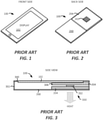
- FIGS. 1-3 illustrate an example of a mobile device that includes a heat spreader for dissipating heat generated by a chip.
- the mobile device 100 includes a display 102, a back side surface 200, a die 202, and a heat spreader 204.
- the die 202 and the heat spreader 204 which are both shown with dotted lines, are located inside the mobile device 100.
- the die 202 is coupled to a first surface of the heat spreader 204.
- a second surface of the heat spreader 204 is coupled to a first surface (e.g., inner surface) of the back side surface 200.
- FIG. 3 illustrates a profile view of the mobile device 100 that includes the heat spreader 204.
- the mobile device 100 includes the display 102, the back side surface 200, a front side surface 300, a bottom side surface 302, and a top side surface 304.
- FIG. 3 also illustrates a printed circuit board (PCB) 306, the die 202 and the heat spreader 204 inside the mobile device 100.
- PCB printed circuit board
- a first side of the die 202 is coupled to a first surface of the PCB 306.
- a second side of the die 202 is coupled to a first surface of the heat spreader 204.
- a second surface of the heat spreader 204 is coupled to a first surface (e.g., inner surface) of the back side surface 200.
- this will cause the back side surface 200 to heat up to a temperature that is higher than was is comfortable and/or acceptable to a user (e.g., person) holding the mobile device.
- the temperature of the back side surface 200 of the mobile device may be even hot enough to burn a user touching and/or holding the mobile device 100.
- the publication US2010321895 is a further example of the prior art.
- Various apparatus and methods described herein provide a multi-layer heat dissipating apparatus for an electronic device.
- a first example provides a multi-layer heat dissipating device that includes a first heat spreader layer, a first support structure, and a second heat spreader layer.
- the first heat spreader layer includes a first spreader surface and a second spreader surface.
- the first support structure includes a first support surface and a second support surface.
- the first support surface of the first support structure is coupled to the second spreader surface of the first heat spreader.
- the second heat spreader layer includes a third spreader surface and a fourth spreader surface.
- the third spreader surface of the second heat spreader layer is coupled to the second support surface of the first support structure.
- the first heat spreader layer has a first thermal conductivity
- the first support structure has a second thermal conductivity that is less than the first thermal conductivity.
- the first support structure comprises a thermally conductive adhesive layer.
- the first support structure is coupled to the first heat spreader layer through a thermally conductive adhesive layer.
- the multi-layer heat dissipating device further includes (i) a second support structure comprising a third support surface and a fourth support surface, wherein the third support surface of the second support structure is coupled to the fourth spreader surface of the second heat spreader, and (ii) a third heat spreader layer comprising a fifth spreader surface and a sixth spreader surface, wherein the fifth spreader surface of the third heat spreader layer is coupled to the fourth support surface of the second support structure.
- the first support structure has a first size
- the second support structure has a second size that is greater than the first size.
- the second heat spreader layer has a third thermal conductivity
- the second support structure has a fourth thermal conductivity that is less than the third thermal conductivity.
- the first surface of the first heat spreader layer is coupled to a heat generating region and/or a region configured to generate heat.
- the first heat spreader layer includes a first set of fins.
- the first surface of the first heat spreader layer is coupled to at least one heat generating component and/or component configured to generate heat when active.
- the first heat spreader layer, the first support structure, and the second heat spreader layer are coupled together so as to form and encapsulate a gap in the multi-layer heat dissipating device.
- the first heat spreader layer is coupled to the heat generating component through a thermal interface material.
- the second surface of the second heat spreader layer is coupled to an inner portion of a first surface of an electronic device.
- the multi-layer heat dissipating device is incorporated into at least one of a music player, a video player, an entertainment unit, a navigation device, a communications device, a mobile device, a mobile phone, a smartphone, a personal digital assistant, a fixed location terminal, a tablet computer, and/or a laptop computer.
- a second example provides an apparatus that includes (i) a first heat spreading means for dissipating heat, (ii) a first supporting means coupled to the first heat spreading means, and (iii) a second heat spreading means for dissipating heat, wherein the second heat spreading means is coupled to the first supporting means.
- the first heat spreading means has a first thermal conductivity
- the first supporting means has a second thermal conductivity that is less than the first thermal conductivity
- the first supporting means is coupled to the first heat spreading means through a thermally conductive adhesive means.
- the apparatus includes (i) a second supporting means coupled to the second heat spreading means, (ii) and a third heat spreading means for dissipating heat, wherein the third heat spreading means is coupled to the second supporting means.
- the first heat spreading means is coupled to a heat generating region and/or a region configured to generate heat.
- the region configured to generate heat includes an integrated package.
- the second heat spreading means is coupled to an inner portion of a first surface of an electronic device.
- the apparatus is incorporated into at least one of a music player, a video player, an entertainment unit, a navigation device, a communications device, a mobile device, a mobile phone, a smartphone, a personal digital assistant, a fixed location terminal, a tablet computer, and/or a laptop computer.
- a third example provides a device that includes a region configured to generate heat.
- the region includes an integrated device.
- the device includes a first heat spreader layer that includes a first spreader surface and a second spreader surface, wherein the first spreader surface of the first heat spreader layer is coupled to the region.
- the device includes a first support structure that includes a first support surface and a second support surface, where the first support surface of the first support structure is coupled to the second spreader surface of the first heat spreader.
- the device includes a second heat spreader layer that includes a third spreader surface and a fourth spreader surface, where the third spreader surface of the second heat spreader layer is coupled to the second support surface of the first support structure.
- the device further includes an electronic device surface, where the electronic device surface is coupled to the fourth spreader surface of the second heat spreader.
- the device further includes a second support structure that includes a third support surface and a fourth support surface, where the third support surface of the second support structure is coupled to the fourth spreader surface of the second heat spreader.
- the device further includes a third heat spreader layer comprising a fifth spreader surface and a sixth spreader surface, where the fifth spreader surface of the third heat spreader layer is coupled to the fourth support surface of the second support structure.
- the device also includes an electronic device surface, where the electronic device surface is coupled to the sixth spreader surface of the third heat spreader.
- the first heat spreader layer has a first thermal conductivity
- the first support structure has a second thermal conductivity that is less than the first thermal conductivity
- the first spreader surface of the first heat spreader layer is coupled to the integrated device.
- the region includes a printed circuit board (PCB).
- PCB printed circuit board
- the device is incorporated into at least one of a music player, a video player, an entertainment unit, a navigation device, a communications device, a mobile device, a mobile phone, a smartphone, a personal digital assistant, a fixed location terminal, a tablet computer, and/or a laptop computer.
- Some exemplary embodiments of this disclosure pertain to a multi-layer heat dissipating device that includes a first heat spreader layer, a first support structure, and a second heat spreader layer.
- the first heat spreader layer includes a first spreader surface and a second spreader surface.
- the first support structure includes a first support surface and a second support surface. The first support surface of the first support structure is coupled to the second spreader surface of the first heat spreader.
- the second heat spreader layer includes a third spreader surface and a fourth spreader surface. The third spreader surface of the second heat spreader layer is coupled to the second support surface of the first support structure.
- the first support structure is a thermally conductive adhesive layer.
- the first heat spreader layer has a first thermal conductivity
- the first support structure has a second thermal conductivity that is less than the first thermal conductivity.
- the first surface of the first heat spreader layer is coupled to a heat generating region and/or a region configured to generate heat.
- the heat generating region and/or region configured to generate heat includes one of at least an integrated package, a die, a die package, a system-on-chip (SoC) and/or a printed circuit board (PCB).
- the second surface of the second heat spreader layer is coupled to an inner portion of a first surface of an electronic device (e.g., mobile device).
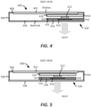
- FIG. 4 illustrates an electronic device 400 (e.g., mobile device) that includes a display 402, a front side surface 404, a back side surface 406, a bottom side surface 408, and a top side surface 410.
- the electronic device 400 also includes a printed circuit board (PCB) 420, an integrated device 422 (e.g., chip, die, die package), and a multi-layer heat dissipating device 430 (e.g., heat spreader).
- PCB printed circuit board
- FIG. 4 illustrates a multi-layer heat dissipating device 430 in physical contact with the back side surface 406 and the top side surface 410 of the electronic device 400.
- a multi-layer heat dissipating device may be near (e.g., in close proximity of) the back side surface 406 and/or the top side surface 410 of the electronic device 400, but not in physical contact with the back side surface 406 and/or the top side surface 410 of the electronic device 400.
- FIG. 5 Such an example will further be described in FIG. 5 .
- the integrated device 422 is part of a heat generating component, a heat generating region, and/or a region configured to generate heat in the electronic device 400.
- the PCB 420 is part of a heat generating component, a heat generating region and/or region configured to generate heat in the electronic device 400.
- the PCB 420 has a first surface and a second surface that is opposite to the first surface.
- the integrated device 422 has a first surface and a second surface that is opposite to the first surface. As shown in FIG. 4 , the first surface of the integrated device 422 is coupled to the second surface of the PCB 420.
- the multi-layer heat dissipating device 430 includes a first heat spreader layer 432, a first support structure 433, and a second heat spreader layer 434.
- the first heat spreader layer 432 has a first surface and a second surface that is opposite to the first surface.
- the first support structure 433 has a first surface and a second surface that is opposite to the first surface.
- the second heat spreader layer 434 has a first surface and a second surface that is opposite to the first surface.
- the second surface of the first heat spreader layer 432 is coupled to the first surface of the first support structure 433.
- the second surface of the first support structure 433 is coupled to the first surface of the second heat spreader layer 434.
- the first support structure 433 is a thermally conductive adhesive layer.
- the first surface of the first heat spreader layer 432 is coupled to the integrated device 422 (e.g., second surface of the integrated device 422).
- the first heat spreader layer 432 is coupled to the integrated device 422 through a thermal interface material (e.g., thermally conductive adhesive).
- the first surface of the first heat spreader layer 432 is coupled to a heat generating region and/or a region configured to generate heat that includes the integrated device 422.
- the second surface of the second heat spreader layer 434 is coupled to a first surface (e.g., inner surface) of the back side surface 406 of the electronic device 400.
- a side portion of the first heat spreader layer 432, and/or a side portion of the second heat spreader layer 434 may be coupled (e.g., touching) to a first surface (e.g., inner surface) of the top side surface 410 of the electronic device 400.
- the multi-layer heat dissipating device 430 is configured in such a way that heat from a heat generating region and/or region configured to generate heat (e.g., region that includes the integrated device 422) dissipates laterally and vertically from the heat dissipating device 430.
- heat from the heat generating region and/or region configured to generate heat may dissipate laterally from the first heat spreader layer 432 and the second heat spreader layer 434 into the inner region of the electronic device 400.
- heat from the heat generating region and/or region configured to generate heat may also dissipate through the top side surface 410. Heat from the heat generating region and/or region configured to generate heat may also dissipate through the back side surface 406.
- the multi-layer heat dissipating device 430 is configured to spread out the dissipation of heat through different directions and/or surfaces, instead of entirely (or mostly) through the back side surface 406 of the electronic device 400. That is, some of the heat that would have otherwise dissipated through the back side surface 406 is now dissipated laterally to the inside of the electronic device 400 (thus reducing a hot spot peak temperature on the surface 406) and/or through the top side surface 410 of the electronic device. By doing this, it reduces and/or prevents the back side surface 406 of the electronic device 400 from reaching a temperature that is higher than a temperature threshold (e.g., temperature threshold that is acceptable or comfortable for a user of the electronic device 400).
- a temperature threshold e.g., temperature threshold that is acceptable or comfortable for a user of the electronic device 400.
- the heat dissipating device 430 is configured in such a way as to maximize lateral heat dissipation and minimize vertical heat dissipation (or at least reduce vertical heat dissipation), which would reduce the likelihood of hotspot peak temperatures on the surface of the electronic device. In some implementations, this can be achieved by having at least one heat spreader layer with a high thermal conductivity value coupled to a support structure (and/or adhesive materials) with a low thermal conductivity value. In some implementations, the materials for the heat spreader layer and the support structure are chosen to maximize the difference between the high thermal conductivity value of the heat spreader layer and the low thermal conductivity value of the support structure. Examples of thermal conductivity values will be further described below.
- a support structure that has a low thermal conductivity provides greater thermal conductivity resistance than a heat spreader layer with a high thermal conductivity.
- This thermal conductivity resistance in the support structure encourages or forces the heat to substantially escape or dissipate through the heat spreader layer.
- heat from a heat generating region and/or region configured to generate heat substantially and laterally dissipates through the heat spreader layer.
- the support structure with the low thermal conductivity in essence provides a vertical thermal resistance to the heat, which substantially shields the surface of the electronic device from the heat that is being generated from the heat generating region and/or region configured to generate heat (e.g., region comprising integrated circuit).
- gaps e.g., air gaps, vacuum
- the gap is located within a region or volume surrounded by the first heat spreader layer 432, the support structure 433, and the second heat spreader layer 434.
- first heat spreader layer 432 may be made of a material that includes one of at least metal, carbon, graphite and/or aluminum.
- first heat spreader layer 432 has a first thermal conductivity value
- first support structure 433 has a second thermal conductivity value
- second heat spreader layer 434 has a third thermal conductivity value.
- a particular thermal conductivity value of a particular material quantifies how well or how poorly a particular material conducts heat.
- the material, the shape, and/or the thermal conductivity value of the first support structure 433 is chosen, such that heat from the heat generating region and/or region configured to generate heat (e.g., region that includes the integrated device 422) is primarily dissipated through the first heat spreader layer 432.
- the first support structure 433 is configured to provide thermal resistance (e.g., vertical thermal resistance of the heat dissipating device) of heat from the heat generating region and/or region configured to generate heat, which would cause more heat to dissipate through the first heat spreader layer 432 (e.g., more heat to dissipate laterally).
- the second thermal conductivity of the first support structure 433 is less than the first thermal conductivity of the first heat spreader layer 432. It should be noted that heat may still dissipate through the second heat spreader layer 434 and the back side surface 406, but not as much without the first support structure 433. Examples of different shapes for support structures are further described and illustrated in FIGS. 10-14 .
- the first support structure 433 is coupled to the first heat spreader layer 432 through an adhesive material (e.g., thermally conductive adhesive layer). Similarly, in some implementations, the first support structure 433 is coupled to the second heat spreader layer 434 through an adhesive material (e.g., thermally conductive adhesive layer). Different implementations may use different materials for the first support structure 433 and/or the adhesive material. Examples of materials for the first support structure 433 and/or the adhesive material (e.g., thermally conductive adhesive layer) include an epoxy or porous material (e.g., material with air gaps).
- the first support structure 433 and/or the adhesive material are configured to provide mechanical support for the multi-layer heat dissipating device 430 while minimizing the amount of heat conduction in the vertical direction of the heat dissipating device 430 and maximizing heat conduction in the lateral direction of the heat dissipating device 430.
- the use of one or more adhesive materials to couple a support structure to a heat spreader layer is not limited to the multi-layer heat dissipating device 430 of FIG. 4 .
- the adhesive materials may be used to couple a support structure to a heat spreader layer in any of the multi-layer heat dissipating device described in the present disclosure.
- the multi-layer heat dissipating device 430 has a first dimension, a second dimension, and a third dimension.
- the first dimension is a height of the multi-layer heat dissipating device, which may be along a Z-direction.
- the Z-direction is a vertical direction.
- a vertical direction is a direction along the multi-layer heat dissipating device 430 that traverses (e.g., perpendicularly) the heat spreader layer(s) and the support structure.
- a vertical direction is a direction that is perpendicular or orthogonal to a surface of the heat spreader having the biggest surface area.
- the vertical direction is perpendicular or orthogonal to the top surface of an integrated device (e.g., die, chip), and/or printed circuit board (PCB).
- PCB printed circuit board
- the second dimension is a length of the multi-layer heat dissipating device, which may be along a Y-direction. In some implementations, the Y-direction is a lateral direction. In some implementations, the second dimension is a radius of the multi-layer heat dissipating device, which may be along a Y-direction.
- the third dimension is a width of the multi-layer heat dissipating device, which may be along an X-direction. In some implementations, the X-direction is a lateral direction.
- Examples of X, Y, Z dimensions and/or directions for a multi-layer heat dissipating devices are shown in at least FIGS. 7 , 9 , 18 and 20 .
- FIG. 4 illustrates an example of an apparatus (e.g., multi-layer heat dissipating device 430, electronic device 400) that includes a first heat spreading means (e.g., first heat spreader layer 432), a first supporting means (e.g., first support structure 433), and a second heat spreading means (e.g., second heat spreader layer 434).
- a first heat spreading means e.g., first heat spreader layer 432
- a first supporting means e.g., first support structure 433
- a second heat spreading means e.g., second heat spreader layer 434
- at least one of the heat spreading means has a high thermal conductivity value.
- at least one of the supporting means has a low thermal conductivity value. Examples of high and low thermal conductivity values will be further described below.
- Different implementations may use materials with different thermal conductivity values for the support structures, the heat spreader layers, the thermal interface layers and/or the adhesive materials (e.g., thermally conductive adhesive layers).
- the support structures are made of a material with a low thermal conductivity value.
- at least one of the support structures has a thermal conductivity value of about 0.3 watts per meter kelvin (W/m ⁇ k) or less.
- a low thermal conductivity value is about 0.3 watts per meter kelvin (W/m ⁇ k) or less.
- At least one of the heat spreader layer is made of a material that includes one of at least metal, carbon, graphite and/or aluminum. In some implementations, at least one of the heat spreader layers is made of a material with a high thermal conductivity value. In some implementations, at least one of the heat spreader layer has a thermal conductivity value of about 300 W/m ⁇ k or higher. In some implementations, at least one of the heat spreader layer has a thermal conductivity value of about 500 W/m ⁇ k or higher (e.g., graphite). In some implementations, a high thermal conductivity value is about 300 W/m ⁇ k or higher.
- a thermal interface layer is a material used to couple a heat spreader layer and an integrated device.
- thermal interfaces layers include solder, epoxy, metal filled attach, etc...
- at least one of the thermal interface layers has a thermal conductivity value of about 1.5W/m ⁇ k or less. In some implementations, at least one of the thermal interface layers has a thermal conductivity value of between about 0.7-1.5W/m ⁇ k.
- an adhesive material e.g., thermally conductive adhesive layer
- at least one of the thermal interface layers has a thermal conductivity value that is about equal or greater than the thermal conductivity value of the support structure.
- at least one of the thermal interface layers has a thermal conductivity value that is about equal or less than the thermal conductivity value of the thermal interface layer.
- thermal conductivity values are merely examples, and the materials used in a multi-layer heat dissipating device are not limited to materials that have these thermal conductivity values.
- FIG. 4 illustrates the multi-layer heat dissipating device 430 in a first location inside the electronic device 400.
- FIG. 4 illustrates a multi-layer heat dissipating device 430 in physical contact (e.g., touching) with the back side surface of the electronic device 400.
- the multi-layer heat dissipating device may be located in a different location inside the electronic device 400.
- FIG. 5 illustrates an electronic device 500 that includes a multi-layer heat dissipating device 530 in a second location inside the electronic device 500, where the second location is different than the first location of FIG. 4 .
- the multi-layer heat dissipating device 530 of FIG. 5 is similar to the multi-layer heat dissipating device 430 of FIG. 4 , except that the multi-layer heat dissipating device 530 is positioned differently in the electronic device 500.
- the electronic device 500 (e.g., mobile device) includes a display 502, a front side surface 504, a back side surface 506, a bottom side surface 508, and a top side surface 510.
- the electronic device 500 also includes a printed circuit board (PCB) 520, an integrated device 522 (e.g., chip, die, die package), and the multi-layer heat dissipating device 530 (e.g., heat spreader).
- PCB printed circuit board
- the integrated device 522 is part of a heat generating component, a heat generating region, and/or a region configured to generate heat in the electronic device 500.
- the PCB 520 is part of a heat generating component, a heat generating region and/or region configured to generate heat in the electronic device 500.
- the PCB 520 has a first surface and a second surface that is opposite to the first surface.
- the integrated device 522 has a first surface and a second surface that is opposite to the first surface. As shown in FIG. 5 , the first surface of the integrated device 522 is coupled to the second surface of the PCB 520.
- the multi-layer heat dissipating device 530 includes a first heat spreader layer 532, a first support structure 533, and a second heat spreader layer 534.
- the heat dissipating device 530 is configured in such a way as to maximize lateral heat dissipation and minimize vertical heat dissipation (or at least reduce vertical heat dissipation), which would reduce the likelihood of hotspot peak temperatures on the surface of the electronic device. In some implementations, this can be achieved by having at least one heat spreader layer with a high thermal conductivity value coupled to a support structure (and/or adhesive materials) with a low thermal conductivity value. In some implementations, the materials for the heat spreader layer and the support structure are chosen to maximize the difference between the high thermal conductivity value of the heat spreader layer and the low thermal conductivity value of the support structure.
- the side portion of the first heat spreader layer 532 and the side portion of the second heat spreader layer 534 do not touch the top side surface 510 of the electronic device 500. That is, there is a gap (e.g., air gap) between the first heat spreader layer 532 and the top side surface 510. Similarly, there is a gap (e.g., air gap) between the second heat spreader layer 534 and the top side surface 510. In addition, there is also a gap (e.g., air gap) between the second heat spreader layer 534 and the back side surface 506 of the electronic device 500.
- a gap e.g., air gap
- first heat spreader layer 532 and the second heat spreader layer 534 do not touch the back side surface 506 and/or the top side surface 510, heat from a heat generating region and/or region configured to generate heat (e.g., region that includes the integrated device 522) may still dissipate through the back side surface 506 and/or the top side surface 510 of the electronic device 500.
- the gap between the multi-layer heat dissipating device 530 and the surface of the electronic device 500 provides enough thermal resistance to prevent the surface of the electronic device 500 from reaching a hotspot temperature or undesirable temperature.
- FIG. 5 illustrates an example of an apparatus (e.g., multi-layer heat dissipating device 530, electronic device 500) that includes a first heat spreading means (e.g., first heat spreader layer 532), a first supporting means (e.g., first support structure 533), and a second heat spreading means (e.g., second heat spreader layer 534).
- a first heat spreading means e.g., first heat spreader layer 532
- a first supporting means e.g., first support structure 533
- a second heat spreading means e.g., second heat spreader layer 534
- at least one of the heat spreading means has a high thermal conductivity value.
- at least one of the supporting means has a low thermal conductivity value.
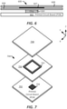
- FIG. 6 illustrates a close-up view of a multi-layer heat dissipating device coupled to an integrated device.
- a multi-layer heat dissipating device 600 e.g., heat spreader
- the heat generating components may include at least one of a printed circuit board (PCB) 602 and/or an integrated device 604 (e.g., chip, die, die package).
- a heat generating region may include at least one of a printed circuit board (PCB) 602 and/or an integrated device 604 (e.g., chip, die, die package).
- a region configured to generate heat may include at least one of a printed circuit board (PCB) 602 and/or an integrated device 604 (e.g., chip, die, die package).
- the PCB 602 has a first surface and a second surface that is opposite to the first surface.
- the integrated device 604 has a first surface and a second surface that is opposite to the first surface. As shown in FIG. 6 , the first surface of the integrated device 604 is coupled to the second surface of the PCB 602.
- the multi-layer heat dissipating device 600 includes a first heat spreader layer 606, a first support structure 607, and a second heat spreader layer 608.
- the first heat spreader layer 606 has a first surface and a second surface that is opposite to the first surface.
- the first support structure 607 has a first surface and a second surface that is opposite to the first surface.
- the second heat spreader layer 608 has a first surface and a second surface that is opposite to the first surface.
- the second surface of the first heat spreader layer 606 is coupled to the first surface of the first support structure 607.
- the second surface of the first support structure 607 is coupled to the first surface of the second heat spreader layer 608.
- the first support structure 607 is an adhesive layer (e.g., a thermally conductive adhesive layer).
- the first surface of the first heat spreader layer 606 is coupled to the integrated device 604 (e.g., second surface of the integrated device 604) through a thermal interface material (e.g., thermally conductive adhesive). In some implementations, the first surface of the first heat spreader layer 606 is coupled to a heat generating region and/or a region configured to generate heat that includes the integrated device 604.
- a thermal interface material e.g., thermally conductive adhesive
- the heat dissipating device 600 is configured in such a way as to maximize lateral heat dissipation and minimize vertical heat dissipation (or at least reduce vertical heat dissipation), which would reduce the likelihood of hotspot peak temperatures on the surface of the electronic device. In some implementations, this can be achieved by having heat spreader layer (e.g., heat spreader layer 606) with a high thermal conductivity value coupled to a support structure (e.g., support structure 607) with a low thermal conductivity value. In some implementations, the materials for the heat spreader layer and the support structure are chosen to maximize the difference between the high thermal conductivity value of the heat spreader layer and the low thermal conductivity value of the support structure.
- heat spreader layer e.g., heat spreader layer 606
- a support structure e.g., support structure 607
- the materials for the heat spreader layer and the support structure are chosen to maximize the difference between the high thermal conductivity value of the heat spreader layer and the low thermal conductivity value of the support structure
- FIG. 7 illustrates an assembly view of the different components of an integrated device and a multi-layer heat dissipating device.
- a multi-layer heat dissipating device 700 e.g., heat spreader
- the heat generating components may include at least one of a printed circuit board (PCB) 702 and/or an integrated device 704 (e.g., chip, die, die package).
- a heat generating region may include at least one of a printed circuit board (PCB) 702 and/or an integrated device 704 (e.g., chip, die, die package).
- a region configured to generate heat may include at least one of a printed circuit board (PCB) 702 and/or an integrated device 704 (e.g., chip, die, die package).
- the PCB 702 has a first surface and a second surface that is opposite to the first surface.
- the integrated device 704 has a first surface and a second surface that is opposite to the first surface. As shown in FIG. 7 , the first surface of the integrated device 704 is coupled to the second surface of the PCB 702.
- the multi-layer heat dissipating device 700 includes a first heat spreader layer 706, a first support structure 707, and a second heat spreader layer 708.
- the first heat spreader layer 706 has a first surface and a second surface that is opposite to the first surface.
- the first support structure 707 has a first surface and a second surface that is opposite to the first surface.
- the second heat spreader layer 708 has a first surface and a second surface that is opposite to the first surface.
- the second surface of the first heat spreader layer 706 is coupled to the first surface of the first support structure 707.
- the second surface of the first support structure 707 is configured to couple to the first surface of the second heat spreader layer 708.
- the first surface of the first heat spreader layer 706 is configured to couple to the integrated device 704 (e.g., second surface of the integrated device 704).
- the first surface of the first heat spreader layer 706 is configured to couple to a heat generating region that includes the integrated device 704.
- the heat dissipating device 700 is configured in such a way as to maximize lateral heat dissipation and minimize vertical heat dissipation (or at least reduce vertical heat dissipation), which would reduce the likelihood of hotspot peak temperatures on the surface of the electronic device. In some implementations, this can be achieved by having heat spreader layer (e.g., heat spreader layer 706) with a high thermal conductivity value coupled to a support structure (e.g., support structure 707) with a low thermal conductivity value. In some implementations, the materials for the heat spreader layer and the support structure are chosen to maximize the difference between the high thermal conductivity value of the heat spreader layer and the low thermal conductivity value of the support structure.
- heat spreader layer e.g., heat spreader layer 706
- a support structure e.g., support structure 707
- the materials for the heat spreader layer and the support structure are chosen to maximize the difference between the high thermal conductivity value of the heat spreader layer and the low thermal conductivity value of the support structure
- FIGS. 4-7 illustrate a multi-layer heat dissipating device coupled to a single integrated device (e.g., chip). However, in some implementations, a multi-layer heat dissipating device may be coupled to more than one integrated device.
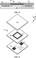
- FIG. 8 illustrates a close-up view of a multi-layer heat dissipating device coupled to two integrated devices.
- FIG. 8 illustrates a multi-layer heat dissipating device 800 (e.g., heat spreader) coupled to heat generating components, a heat generating region and/or region configured to generate heat.
- the heat generating components may include at least one of a printed circuit board (PCB) 802, a first integrated device 803 (e.g., chip, die, die package), and/or a second integrated device 805.
- PCB printed circuit board
- first integrated device 803 e.g., chip, die, die package
- a heat generating region may include at least one of a printed circuit board (PCB) 802, a first integrated device 803 (e.g., chip, die, die package), and/or a second integrated device 805.
- a region configured to generate heat may include at least one of a printed circuit board (PCB) 802, a first integrated device 803 (e.g., chip, die, die package), and/or a second integrated device 805.
- the PCB 802 has a first surface and a second surface that is opposite to the first surface.
- the first integrated device 803 has a first surface and a second surface that is opposite to the first surface.
- the second integrated device 805 has a first surface and a second surface that is opposite to the first surface. As shown in FIG. 8 , the first surface of the first integrated device 803 is coupled to the second surface of the PCB 802. FIG. 8 also illustrates that the first surface of the second integrated device 805 is coupled to the second surface of the PCB 802.
- the multi-layer heat dissipating device 800 includes a first heat spreader layer 806, a first support structure 807, and a second heat spreader layer 808.
- the first heat spreader layer 806 has a first surface and a second surface that is opposite to the first surface.
- the first support structure 807 has a first surface and a second surface that is opposite to the first surface.
- the second heat spreader layer 808 has a first surface and a second surface that is opposite to the first surface.
- the second surface of the first heat spreader layer 806 is coupled to the first surface of the first support structure 807.
- the second surface of the first support structure 807 is coupled to the first surface of the second heat spreader layer 808.
- the first support structure 807 is an adhesive layer (e.g., a thermally conductive adhesive layer).
- the first surface of the first heat spreader layer 806 is coupled to the first integrated device 803 (e.g., second surface of the integrated device 803) through a thermal interface material (e.g., thermally conductive adhesive). In some implementations, the first surface of the first heat spreader layer 806 is coupled to the second integrated device 805 (e.g., second surface of the second integrated device 805) through a thermal interface material (e.g., thermally conductive adhesive). In some implementations, the first surface of the first heat spreader layer 806 is coupled to a heat generating region that includes at least the first integrated device 803 and/or the second integrated device 805. In some implementations, the first integrated device 803 is a central processing unit (CPU) and the second integrated device 805 is a graphical processing unit (GPU).
- CPU central processing unit
- GPU graphical processing unit
- the heat dissipating device 800 is configured in such a way as to maximize lateral heat dissipation and minimize vertical heat dissipation (or at least reduce vertical heat dissipation), which would reduce the likelihood of hotspot peak temperatures on the surface of the electronic device. In some implementations, this can be achieved by having at least one heat spreader layer (e.g., heat spreader layer 806) with a high thermal conductivity value coupled to a support structure (e.g., support structure 807) with a low thermal conductivity value. In some implementations, the materials for the heat spreader layer and the support structure are chosen to maximize the difference between the high thermal conductivity value of the heat spreader layer and the low thermal conductivity value of the support structure.
- FIG. 9 illustrates an assembly view of the different components of an integrated device and a multi-layer heat dissipating device.
- FIG. 9 illustrates a multi-layer heat dissipating device 900 (e.g., heat spreader) and heat generating components, a heat generating region and/or region configured to generate heat.
- the heat generating components may include at least one of a printed circuit board (PCB) 902, a first integrated device 903 (e.g., chip, die, die package), and/or a second integrated device 905.
- PCB printed circuit board
- a heat generating region may include at least one of a printed circuit board (PCB) 902, a first integrated device 903 (e.g., chip, die, die package), and/or a second integrated device 905.
- a region configured to generate may include at least one of a printed circuit board (PCB) 902, a first integrated device 903 (e.g., chip, die, die package), and/or a second integrated device 905.
- the PCB 902 has a first surface and a second surface that is opposite to the first surface.
- the first integrated device 903 has a first surface and a second surface that is opposite to the first surface.
- the second integrated device 905 has a first surface and a second surface that is opposite to the first surface. As shown in FIG. 9 , the first surface of the first integrated device 903 is coupled to the second surface of the PCB 902. The first surface of the second integrated device 905 is also coupled to the second surface of the PCB 902.
- the multi-layer heat dissipating device 900 includes a first heat spreader layer 906, a first support structure 907, and a second heat spreader layer 908.
- the first heat spreader layer 906 has a first surface and a second surface that is opposite to the first surface.
- the first support structure 907 has a first surface and a second surface that is opposite to the first surface.
- the second heat spreader layer 908 has a first surface and a second surface that is opposite to the first surface.
- the second surface of the first heat spreader layer 906 is coupled to the first surface of the first support structure 907.
- the second surface of the first support structure 907 is configured to couple to the first surface of the second heat spreader layer 908.
- the first surface of the first heat spreader layer 906 is configured to couple to the first integrated device 903 (e.g., second surface of the integrated device 903) and the second integrated device 905 (e.g., second surface of the integrated device 905).
- the first surface of the first heat spreader layer 906 is configured to couple a heat generating region that includes the integrated device 903 and the integrated device 905.
- the heat dissipating device 900 is configured in such a way as to maximize lateral heat dissipation and minimize vertical heat dissipation (or at least reduce vertical heat dissipation), which would reduce the likelihood of hotspot peak temperatures on the surface of the electronic device. In some implementations, this can be achieved by having at least one heat spreader layer (e.g., heat spreader layer 906) with a high thermal conductivity value coupled to a support structure (e.g., support structure 907) with a low thermal conductivity value. In some implementations, the materials for the heat spreader layer and the support structure are chosen to maximize the difference between the high thermal conductivity value of the heat spreader layer and the low thermal conductivity value of the support structure.
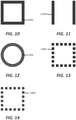
- FIGS. 10 and 12 -14 illustrate examples of different sizes, shapes and/or configurations for a support structure of a multi-layer heat dissipating device.
- the support structures illustrated and described in FIGS. 10 and 12-14 may be implemented in any of the multi-layer heat dissipating device described in the present disclosure.
- FIG. 10 illustrates a support structure 1000 that has the shape of a square perimeter.
- FIG. 11 is an example which is not part of the invention, it illustrates a support structure 1100 that includes a first rectangular structure and a second rectangular structure.
- FIG. 12 illustrates a support structure 1200 that has the shape of a circular ring (e.g., donut shape).
- FIG. 13 illustrates a support structure 1300 that includes several square columns arranged in a square perimeter.
- FIG. 14 illustrates a support structure 1400 that includes several circular columns arranged in a square perimeter.
- the support structures 1000, 1100, 1200, 1300, and/or 1400 are a thermally conductive adhesive layer.
- a heat dissipating device may have more than two heat spreader layers.
- FIG. 15 illustrates an electronic device 1500 (e.g., mobile device) that includes a display 1502, a front side surface 1504, a back side surface 1506, a bottom side surface 1508, and a top side surface 1510.
- the electronic device 1500 also includes a printed circuit board (PCB) 1520, an integrated device 1522 (e.g., chip, die, die package), and a multi-layer heat dissipating device 1530 (e.g., heat spreader).
- PCB printed circuit board
- FIG. 15 illustrates a multi-layer heat dissipating device 1530 in physical contact with the back side surface 1506 and the top side surface 1510 of the electronic device 1500.
- a multi-layer heat dissipating device may be near (e.g., in close proximity of) the back side surface 1506 and/or the top side surface 1510 of the electronic device 1500, but not in physical contact (e.g., not touching) with the back side surface 1506 and/or the top side surface 1510 of the electronic device 1500.
- FIG. 16 Such an example will further be described in FIG. 16 .
- the integrated device 1522 is part of a heat generating component, a heat generating region, and/or a region configured to generate heat in the electronic device 1500.
- the PCB 1520 is part of a heat generating component, a heat generating region, and/or a region configured to generate heat in the electronic device 1500.
- the PCB 1520 has a first surface and a second surface that is opposite to the first surface.
- the integrated device 1522 has a first surface and a second surface that is opposite to the first surface. As shown in FIG. 15 , the first surface of the integrated device 1522 is coupled to the second surface of the PCB 1520.
- the multi-layer heat dissipating device 1530 includes a first heat spreader layer 1532, a first support structure 1533, a second heat spreader layer 1534, a second support structure 1535, and a third heat spreader layer 1536.
- the first heat spreader layer 1532 has a first surface and a second surface that is opposite to the first surface.
- the first support structure 1533 has a first surface and a second surface that is opposite to the first surface.
- the second heat spreader layer 1534 has a first surface and a second surface that is opposite to the first surface.
- the second support structure 1535 has a first surface and a second surface that is opposite to the first surface.
- the third heat spreader layer 1536 has a first surface and a second surface that is opposite to the first surface.
- FIG. 15 illustrates that the second support structure 1535 is greater (e.g., wider, longer, bigger diameter, bigger circumference) than the first support structure 1533.
- the second surface of the first heat spreader layer 1532 is coupled to the first surface of the first support structure 1533.
- the second surface of the first support structure 1533 is coupled to the first surface of the second heat spreader layer 1534.
- the second surface of the second heat spreader layer 1534 is coupled to the first surface of the second support structure 1535.
- the second surface of the second support structure 1535 is coupled to a first surface of the third heat spreader layer 1536.
- the first support structure 1533 and/or the second support structure 1535 is a thermally conductive adhesive layer.
- the first surface of the first heat spreader layer 1532 is coupled to the integrated device 1522 (e.g., second surface of the integrated device 1522).
- the first heat spreader layer 1532 is coupled to the integrated device 1522 through a thermal interface material (e.g., thermally conductive adhesive).
- the first surface of the first heat spreader layer 1532 is coupled a heat generating region that includes the integrated device 1522.
- the second surface of the third heat spreader layer 1536 is coupled to a first surface (e.g., inner surface) of the back side surface 1506 of the electronic device 1500.
- a side portion of the first heat spreader layer 1532, a side portion of the second heat spreader layer 1534, and/or a side portion of the third heat spreader layer 1536 may be coupled to a first surface (e.g., inner surface) of the top side surface 1510 of the electronic device 1500.
- the multi-layer heat dissipating device 1530 is configured in such a way that heat from a heat generating region (e.g., region that includes the integrated device 1522) dissipates laterally and vertically from the heat dissipating device 1530.
- heat from the heat generating region may dissipate laterally from the first heat spreader layer 1532, the second heat spreader layer 1534, and the third heat spreader layer 1536 into the inner region of the electronic device 1500.
- heat from the heat generating region may also dissipate through the top side surface 1510. Heat from the heat generating region may also dissipate through the back side surface 1506.
- the multi-layer heat dissipating device 1530 is configured to spread out the dissipation of heat through different directions and/or surfaces, instead of entirely (or mostly) through the back side surface 1506 of the electronic device 1500. That is, some of the heat that would have otherwise dissipated through the back side surface 1506 is now dissipated to the inside of the electronic device 1500 and/or through the top side surface 1510 of the electronic device. By doing this, it reduces and/or prevents the back side surface 1506 of the electronic device 1500 from reaching a temperature that is higher than a temperature threshold (e.g., temperature threshold that is acceptable or comfortable for a user of the electronic device 1500).
- a temperature threshold e.g., temperature threshold that is acceptable or comfortable for a user of the electronic device 1500.
- the heat dissipating device 1530 is configured in such a way as to maximize lateral heat dissipation and minimize vertical heat dissipation (or at least reduce vertical heat dissipation), which would reduce the likelihood of hotspot peak temperatures on the surface of the electronic device. In some implementations, this can be achieved by having at least one heat spreader layer (e.g., heat spreader layer 1532) with a high thermal conductivity value coupled to a support structure (e.g., support structure 1533) with a low thermal conductivity value. In some implementations, the materials for the heat spreader layer and the support structure are chosen to maximize the difference between the high thermal conductivity value of the heat spreader layer and the low thermal conductivity value of the support structure.
- first heat spreader layer 1532, the first support structure 1533, the second heat spreader layer 1534, the second support structure 1535, and the third heat spreader layer 1536 may be made of a material that includes one of at least metal and/or aluminum.
- the first heat spreader layer 1532 has a first thermal conductivity value
- the first support structure 1533 has a second thermal conductivity value
- the second heat spreader layer 1534 has a third thermal conductivity value
- the second support structure 1535 has a fourth thermal conductivity value
- the third heat spreader layer 1536 has a fifth thermal conductivity value.
- a particular thermal conductivity value of a particular material quantifies how well or how poorly a particular material conducts heat.
- the material, the shape, and/or the thermal conductivity value of the first support structure 1533 and/or the second support structure 1535 is chosen, such that heat from the heat generating region (e.g., region that includes the integrated device 1522) is primarily (or mostly) dissipated through the first heat spreader layer 1532 and/or the second heat spreader layer 1534.
- the first support structure 1533 is configured to provide thermal resistance (e.g., vertical thermal resistance of the heat dissipating device) of heat from the heat generating region, which would cause more heat to dissipate through the first heat spreader layer 1532 (e.g., heat to dissipate laterally).
- the second thermal conductivity of the first support structure 1533 is less than the first thermal conductivity of the first heat spreader layer 1532.
- the second support structure 1535 is configured to provide thermal resistance (e.g., vertical thermal resistance of the heat dissipating device) of heat from the heat generating region, which would cause more heat to dissipate through the second heat spreader layer 1534.
- the fourth thermal conductivity of the second support structure 1535 is less than the third thermal conductivity of the second heat spreader layer 1534.
- heat may still dissipate through the third heat spreader layer 1536 and the back side surface 1506, but not as much without the first support structure 1533 and/or the second support structure 1535. Examples of different shapes for support structures were previously described and illustrated in FIGS. 10-14 .
- FIG. 15 illustrates an example of an apparatus (e.g., multi-layer heat dissipating device 1530, electronic device 1500) that includes a first heat spreading means (e.g., first heat spreader layer 1532), a first supporting means (e.g., first support structure 1533), a second heat spreading means (e.g., second heat spreader layer 1534), a second supporting means (e.g., second support structure 1535), and a third heat spreading means (e.g., third heat spreader layer 1536).
- a first heat spreading means e.g., first heat spreader layer 1532
- a first supporting means e.g., first support structure 1533
- a second heat spreading means e.g., second heat spreader layer 1534
- a second supporting means e.g., second support structure 1535
- a third heat spreading means e.g., third heat spreader layer 1536
- at least one of the heat spreading means has a high thermal conductivity value.
- FIG. 15 illustrates the multi-layer heat dissipating device 1530 in a first location inside the electronic device 1500.
- FIG. 15 illustrates a multi-layer heat dissipating device 1530 in physical contact with the back side surface of the electronic device 1530.
- the multi-layer heat dissipating device may be located in a different location inside the electronic device 1500.
- FIG. 16 illustrates an electronic device 1600 that includes a multi-layer heat dissipating device 1630 in a second location inside the electronic device 1600, where the second location is different than the first location of FIG. 15 .
- the multi-layer heat dissipating device 1630 of FIG. 16 is similar to the multi-layer heat dissipating device 1530 of FIG. 15 , except that the multi-layer heat dissipating device 1630 is positioned differently in the electronic device 1600.
- FIG. 16 illustrates an electronic device 1600 (e.g., mobile device) that includes a display 1602, a front side surface 1604, a back side surface 1606, a bottom side surface 1608, and a top side surface 1610.
- the electronic device 1600 also includes a printed circuit board (PCB) 1620, an integrated device 1622 (e.g., chip, die, die package), and the multi-layer heat dissipating device 1630 (e.g., heat spreader).
- PCB printed circuit board
- the integrated device 1622 is part of a heat generating component, a heat generating region, and/or a region configured to generate heat in the electronic device 1600.
- the PCB 1620 is part of a heat generating component, a heat generating region, and/or a region configured to generate heat in the electronic device 1600.
- the multi-layer heat dissipating device 1630 includes a first heat spreader layer 1632, a first support structure 1633, a second heat spreader layer 1634, a second support structure 1635, and a third heat spreader layer 1636.
- the first support structure 1633 and/or the second support structure 1635 is a thermally conductive adhesive layer.
- the heat dissipating device 1630 is configured in such a way as to maximize lateral heat dissipation and minimize vertical heat dissipation (or at least reduce vertical heat dissipation), which would reduce the likelihood of hotspot peak temperatures on the surface of the electronic device. In some implementations, this can be achieved by having at least one heat spreader layer with a high thermal conductivity value coupled to a support structure (and/or adhesive materials) with a low thermal conductivity value. In some implementations, the materials for the heat spreader layer and the support structure are chosen to maximize the difference between the high thermal conductivity value of the heat spreader layer and the low thermal conductivity value of the support structure.
- FIG. 16 illustrates that the electronic device 1600 that includes the multi-layer heat dissipating device 1630 in a second location inside the electronic device 1600, where the second location is different than the first location of FIG. 15 .
- the side portion of the first heat spreader layer 1632, the side portion of the second heat spreader layer 1634, and the third heat spreader layer 1636 do not touch the top side surface 1610 of the electronic device 1600.
- the third heat spreader layer 1636 does not touch the back side surface 1606 of the electronic device 1600. That is, there is a gap (e.g., air gap) between the third heat spreader layer 1636 and the surface of the electronic device 1600.
- a gap e.g., air gap
- heat from a heat generating region e.g., region that includes the integrated device 1622
- a heat generating region may still dissipate through the back side surface 1606 and/or the top side surface 1610 of the electronic device 1600.
- FIG. 16 illustrates an example of an apparatus (e.g., multi-layer heat dissipating device 1630, electronic device 1600) that includes a first heat spreading means (e.g., first heat spreader layer 1632), a first supporting means (e.g., first support structure 1633), a second heat spreading means (e.g., second heat spreader layer 1634), a second supporting means (e.g., second support structure 1635), and a third heat spreading means (e.g., third heat spreader layer 1636).
- a first heat spreading means e.g., first heat spreader layer 1632
- a first supporting means e.g., first support structure 1633
- a second heat spreading means e.g., second heat spreader layer 1634
- a second supporting means e.g., second support structure 1635
- a third heat spreading means e.g., third heat spreader layer 1636
- at least one of the heat spreading means has a high thermal conductivity value.
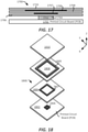
- FIG. 17 illustrates a close-up view of a multi-layer heat dissipating device coupled to an integrated device.
- FIG. 17 illustrates a multi-layer heat dissipating device 1700 (e.g., heat spreader) coupled to heat generating components and/or a heat generating region.
- the heat generating components may include at least one of a printed circuit board (PCB) 1702 and/or an integrated device 1704 (e.g., chip, die, die package).
- a heat generating region may include at least one of a printed circuit board (PCB) 1702 and/or an integrated device 1704 (e.g., chip, die, die package).
- the PCB 1702 has a first surface and a second surface that is opposite to the first surface.
- the integrated device 1704 has a first surface and a second surface that is opposite to the first surface. As shown in FIG. 17 , the first surface of the integrated device 1704 is coupled to the second surface of the PCB 1702.
- the multi-layer heat dissipating device 1700 includes a first heat spreader layer 1706, a first support structure 1707, a second heat spreader layer 1708, a second support structure 1709, and a third heat spreader layer 1710.
- the first heat spreader layer 1706 has a first surface and a second surface that is opposite to the first surface.
- the first support structure 1707 has a first surface and a second surface that is opposite to the first surface.
- the second heat spreader layer 1708 has a first surface and a second surface that is opposite to the first surface.
- the second support structure 1709 has a first surface and a second surface that is opposite to the first surface.
- the third heat spreader layer 1710 has a first surface and a second surface that is opposite to the first surface.
- FIG. 17 illustrates that the second support structure 1709 is greater (e.g., wider, longer, bigger diameter, bigger circumference) than the first support structure 1707.
- the second surface of the first heat spreader layer 1706 is coupled to the first surface of the first support structure 1707.
- the second surface of the first support structure 1707 is coupled to the first surface of the second heat spreader layer 1708.
- the second surface of the second heat spreader layer 1708 is coupled to the first surface of the second support structure 1709.
- the second surface of the second support structure 1709 is coupled to a first surface of the third heat spreader layer 1710.
- the first support structure 1707 and/or the second support structure 1709 is a thermally conductive adhesive layer.
- the first surface of the first heat spreader layer 1706 is coupled to the integrated device 1704 (e.g., second surface of the integrated device 1704).
- the first heat spreader layer 1706 is coupled to the integrated device 1704 through a thermal interface material (e.g., thermally conductive adhesive).
- the first surface of the first heat spreader layer 1706 is coupled to a heat generating region that includes the integrated device 1704.
- the heat dissipating device 1700 is configured in such a way as to maximize lateral heat dissipation and minimize vertical heat dissipation (or at least reduce vertical heat dissipation), which would reduce the likelihood of hotspot peak temperatures on the surface of the electronic device. In some implementations, this can be achieved by having at least one heat spreader layer (e.g., heat spreader layer 1706) with a high thermal conductivity value coupled to a support structure (e.g., support structure 1707) with a low thermal conductivity value. In some implementations, the materials for the heat spreader layer and the support structure are chosen to maximize the difference between the high thermal conductivity value of the heat spreader layer and the low thermal conductivity value of the support structure.
- at least one heat spreader layer e.g., heat spreader layer 1706
- a support structure e.g., support structure 1707
- the materials for the heat spreader layer and the support structure are chosen to maximize the difference between the high thermal conductivity value of the heat spreader layer and the
- FIG. 18 illustrates an assembly view of the different components of an integrated device and a multi-layer heat dissipating device.
- FIG. 18 illustrates a multi-layer heat dissipating device 1800 (e.g., heat spreader) and heat generating components and/or a heat generating region.
- the heat generating components may include at least one of a printed circuit board (PCB) 1802 and/or an integrated device 1804 (e.g., chip, die, die package).
- a heat generating region may include at least one of a printed circuit board (PCB) 1802 and/or an integrated device 1804 (e.g., chip, die, die package).
- the PCB 1802 has a first surface and a second surface that is opposite to the first surface.
- the integrated device 1804 has a first surface and a second surface that is opposite to the first surface. As shown in FIG. 18 , the first surface of the integrated device 1804 is coupled to the second surface of the PCB 1802.
- the multi-layer heat dissipating device 1800 includes a first heat spreader layer 1806, a first support structure 1807, a second heat spreader layer 1808, a second support structure 1809, and a third heat spreader layer 1810.
- the first heat spreader layer 1806 has a first surface and a second surface that is opposite to the first surface.
- the first support structure 1807 has a first surface and a second surface that is opposite to the first surface.
- the second heat spreader layer 1808 has a first surface and a second surface that is opposite to the first surface.
- the second support structure 1809 has a first surface and a second surface that is opposite to the first surface.
- the third heat spreader layer 1810 has a first surface and a second surface that is opposite to the first surface.
- FIG. 18 illustrates that the second support structure 1809 is greater (e.g., wider, longer, bigger diameter, bigger circumference) than the first support structure 1807.
- the second surface of the first heat spreader layer 1806 is coupled to the first surface of the first support structure 1807.
- the second surface of the first support structure 1807 is configured to couple to the first surface of the second heat spreader layer 1808.
- the second surface of the second heat spreader layer 1808 is coupled to the first surface of the second support structure 1809.
- the second surface of the second support structure 1809 is configured to couple to the first surface of the third heat spreader layer 1810.
- the first surface of the first heat spreader layer 1806 is configured to couple to the integrated device 1804 (e.g., second surface of the integrated device 1804).
- the first surface of the first heat spreader layer 1806 is configured to couple to a heat generating region that includes the integrated device 1804.
- the heat dissipating device 1800 is configured in such a way as to maximize lateral heat dissipation and minimize vertical heat dissipation (or at least reduce vertical heat dissipation), which would reduce the likelihood of hotspot peak temperatures on the surface of the electronic device. In some implementations, this can be achieved by having at least one heat spreader layer (e.g., heat spreader layer 1806) with a high thermal conductivity value coupled to a support structure (e.g., support structure 1807) with a low thermal conductivity value. In some implementations, the materials for the heat spreader layer and the support structure are chosen to maximize the difference between the high thermal conductivity value of the heat spreader layer and the low thermal conductivity value of the support structure.
- FIG. 19 illustrates a close-up view of a multi-layer heat dissipating device coupled to two integrated devices.
- a multi-layer heat dissipating device 1900 e.g., heat spreader
- the heat generating components may include at least one of a printed circuit board (PCB) 1902, a first integrated device 1903 (e.g., chip, die, die package) and/or a second integrated device 1905.
- a heat generating region may include at least one of a printed circuit board (PCB) 1902 and/or the integrated devices 1903 and/or 1905 (e.g., chip, die, die package).
- the PCB 1902 has a first surface and a second surface that is opposite to the first surface.
- the first integrated device 1903 has a first surface and a second surface that is opposite to the first surface. As shown in FIG. 19 , the first surface of the first integrated device 1903 is coupled to the second surface of the PCB 1902.
- the second integrated device 1905 has a first surface and a second surface that is opposite to the first surface. As shown in FIG. 19 , the first surface of the second integrated device 1905 is coupled to the second surface of the PCB 1902.
- the multi-layer heat dissipating device 1900 includes a first heat spreader layer 1906, a first support structure 1907, a second heat spreader layer 1908, a second support structure 1909, and a third heat spreader layer 1910.
- the first heat spreader layer 1906 has a first surface and a second surface that is opposite to the first surface.
- the first support structure 1907 has a first surface and a second surface that is opposite to the first surface.
- the second heat spreader layer 1908 has a first surface and a second surface that is opposite to the first surface.
- the second support structure 1909 has a first surface and a second surface that is opposite to the first surface.
- the third heat spreader layer 1910 has a first surface and a second surface that is opposite to the first surface.
- FIG. 19 illustrates that the second support structure 1909 is greater (e.g., wider, longer, bigger diameter, bigger circumference) than the first support structure 1907.
- the second surface of the first heat spreader layer 1906 is coupled to the first surface of the first support structure 1907.
- the second surface of the first support structure 1907 is coupled to the first surface of the second heat spreader layer 1908.
- the second surface of the second heat spreader layer 1908 is coupled to the first surface of the second support structure 1909.
- the second surface of the second support structure 1909 is coupled to a first surface of the third heat spreader layer 1910.
- the first support structure 1907 and/or the second support structure 1909 is a thermally conductive adhesive layer.
- the first surface of the first heat spreader layer 1906 is coupled to the first integrated device 1903 (e.g., second surface of the integrated device 1903) and the second integrated device 1905.
- the first heat spreader layer 1906 is coupled to the first integrated device 1903 and/or the second integrated device 1905 through a thermal interface material (e.g., thermally conductive adhesive).
- the first surface of the first heat spreader layer 1906 is coupled to a heat generating region that includes the first integrated device 1903 and/or the second integrated device 1905.
- the heat dissipating device 1900 is configured in such a way as to maximize lateral heat dissipation and minimize vertical heat dissipation (or at least reduce vertical heat dissipation), which would reduce the likelihood of hotspot peak temperatures on the surface of the electronic device. In some implementations, this can be achieved by having at least one heat spreader layer (e.g., heat spreader layer 1906) with a high thermal conductivity value coupled to a support structure (e.g., support structure 1907) with a low thermal conductivity value. In some implementations, the materials for the heat spreader layer and the support structure are chosen to maximize the difference between the high thermal conductivity value of the heat spreader layer and the low thermal conductivity value of the support structure.
- FIG. 20 illustrates an assembly view of the different components of an integrated device and a multi-layer heat dissipating device.
- FIG. 20 illustrates a multi-layer heat dissipating device 2000 (e.g., heat spreader) and heat generating components and/or a heat generating region.
- the heat generating components may include at least one of a printed circuit board (PCB) 2002, a first integrated device 2003 and/or a second integrated device 2005 (e.g., chip, die, die package).
- a heat generating region may include at least one of a printed circuit board (PCB) 2002, the first integrated device 2003 and/or the second integrated device 2005 (e.g., chip, die, die package).
- the PCB 2002 has a first surface and a second surface that is opposite to the first surface.
- the first integrated device 2003 has a first surface and a second surface that is opposite to the first surface. As shown in FIG. 20 , the first surface of the first integrated device 2003 is coupled to the second surface of the PCB 2002.
- the second integrated device 2005 has a first surface and a second surface that is opposite to the first surface. As shown in FIG. 20 , the first surface of the second integrated device 2005 is coupled to the second surface of the PCB 2002.
- the multi-layer heat dissipating device 2000 includes a first heat spreader layer 2006, a first support structure 2007, a second heat spreader layer 2008, a second support structure 2009, and a third heat spreader layer 2010.
- the first heat spreader layer 2006 has a first surface and a second surface that is opposite to the first surface.
- the first support structure 2007 has a first surface and a second surface that is opposite to the first surface.
- the second heat spreader layer 2008 has a first surface and a second surface that is opposite to the first surface.
- the second support structure 2009 has a first surface and a second surface that is opposite to the first surface.
- the third heat spreader layer 2010 has a first surface and a second surface that is opposite to the first surface.
- FIG. 20 illustrates that the second support structure 2009 is greater (e.g., wider, longer, bigger diameter, bigger circumference) than the first support structure 2007.
- the second surface of the first heat spreader layer 2006 is coupled to the first surface of the first support structure 2007.
- the second surface of the first support structure 2007 is configured to couple to the first surface of the second heat spreader layer 2008.
- the second surface of the second heat spreader layer 2008 is coupled to the first surface of the second support structure 2009.
- the second surface of the second support structure 2009 is configured to couple to the first surface of the third heat spreader layer 2010.
- the first surface of the first heat spreader layer 2006 is configured to couple to the first integrated device 2003 (e.g., second surface of the integrated device 2003) and/or the second integrated device 2005.
- the first surface of the first heat spreader layer 2006 is configured to couple to a heat generating region that includes the first integrated device 2003 and/or the second integrated device 2005.
- the heat dissipating device 2000 is configured in such a way as to maximize lateral heat dissipation and minimize vertical heat dissipation (or at least reduce vertical heat dissipation), which would reduce the likelihood of hotspot peak temperatures on the surface of the electronic device. In some implementations, this can be achieved by having at least one heat spreader layer (e.g., heat spreader layer 2006) with a high thermal conductivity value coupled to a support structure (e.g., support structure 2007) with a low thermal conductivity value. In some implementations, the materials for the heat spreader layer and the support structure are chosen to maximize the difference between the high thermal conductivity value of the heat spreader layer and the low thermal conductivity value of the support structure.
- a heat spreader layer e.g., heat spreader layer 2006
- a support structure e.g., support structure 2007
- the materials for the heat spreader layer and the support structure are chosen to maximize the difference between the high thermal conductivity value of the heat spreader layer and the low thermal conductivity value of
- FIG. 21 illustrates an exemplary method for providing / fabricating a multi-layer heat dissipating device in some implementations.
- the method of FIG. 21 may be used to fabricate any of the multi-layer heat dissipating devices described in the present disclosure.
- the method provides (at 2105) a first heat spreader layer.
- the first heat spreader layer includes a first surface and a second surface opposite of the first surface.
- providing the first heat spreader layer includes fabricating / manufacturing the first heat spreader layer.
- the first heat spreader layer is a high thermal conductivity heat spreader layer.
- the method also provides (at 2110) a first support structure on a first surface of the first heat spreader layer.
- providing the first support structure includes fabricating / manufacturing and coupling (e.g., placing) the first support structure on the first surface of the first heat spreader layer.
- an adhesive layer (e.g., thermally conductive adhesive) is used to couple the first support structure on the first heat spreader layer.
- the first support structure is a thermally conductive adhesive layer.
- the fist support structure is a low thermal conductivity support structure.
- the method provides (at 2115) a second heat spreader layer on the first support structure.
- providing the second heat spreader layer includes fabricating / manufacturing and coupling (e.g., placing) the second heat spreader layer on the first support structure.
- an adhesive layer e.g., thermally conductive adhesive
- the second heat spreader layer is a high thermal conductivity heat spreader layer.
- the method further provides (at 2120) a second support structure on the second heat spreader layer.
- providing the second support structure includes fabricating / manufacturing and coupling (e.g., placing) the second support structure on the second heat spreader layer.
- the second support structure is greater (e.g., wider, longer, bigger circumference, bigger perimeter) than the first support structure.
- an adhesive layer e.g., thermally conductive adhesive
- the second support structure is a thermally conductive adhesive layer.
- the second support structure is a low thermal conductivity support structure.
- the method provides (at 2125) a third heat spreader layer on the second support structure.
- providing the third heat spreader layer includes fabricating / manufacturing and coupling (e.g., placing) the third heat spreader layer on the second support structure.
- an adhesive layer e.g., thermally conductive adhesive
- the third heat spreader layer is a high thermal conductivity heat spreader layer.
- the first heat spreader layer, the first support structure, the second heat spreader layer, the second support structure, and the third heat spreader layer form a multi-layer heat dissipating device that can be implemented in an electronic device.
- the method may further couple (at 2130) the first heat spreader layer of the multi-layer heat dissipating device to heat generating components, a heat generating region and/or region configured to generate heat.
- the heat generating components includes an integrated device (e.g., die, die package) and/or printed circuit board (PCB).
- the heat generating region includes an integrated device (e.g., die, die package) and/or printed circuit board (PCB).
- FIGS. 22, 23 and 24 illustrate three temperature profiles for three electronic devices.
- FIG. 22 illustrates a temperature profile of an electronic device without a heat spreader coupled to an integrated device.
- FIG. 22 illustrates that the maximum temperature of the integrated device (which is conventionally called a junction temperature) is about 114.1 degree Celsius.
- FIG. 22 also illustrates that the maximum surface temperature of the electronic device with a single layer heat spreader is 64.2 degree Celsius.
- FIG. 23 illustrates a temperature profile of an electronic device with a single layer heat spreader coupled to an integrated device.
- FIG. 23 illustrates that the maximum temperature of the integrated device is about 63.7 degree Celsius.
- FIG. 23 also illustrates that the maximum surface temperature of the electronic device with a single layer heat spreader is 47.7 degree Celsius.
- FIG. 24 illustrates a temperature profile of an electronic device that includes a multi-layer heat dissipating device coupled to an integrated device. As shown in FIG. 24 , the maximum temperature of the integrated device is 71.1 degree Celsius. FIG. 24 also illustrates that the maximum surface temperature of the electronic device with a multi-layer heat dissipating device is 44.7 degree Celsius. In some implementations, the multi-layer heat dissipating device, as described in the present disclosure, does a better and more efficient job of dissipating and spreading the heat from the integrated device through the electronic device, than a single layer heat dissipating device, as shown in FIG. 23 .
- FIG. 24 illustrates how the multi-layer heat dissipating devices of the present disclosure provides an efficient and counter intuitive way / method of reducing the heat from an integrated device while at the same time minimizing the heat and/or the temperature that is felt by a user of an electronic device (e.g., mobile device).
- FIGS. 23 and 24 illustrate how a multi-layer heat dissipating device of a same, similar or comparable size to a single layer heat dissipating device can do a more effective and efficient job of dissipating heat from an integrated device without increasing the surface temperature of an electronic device beyond a temperature threshold.
- FIG. 25 illustrates a multi-layer heat dissipating device 2500 with a pyramid configuration.
- the multi-layer heat dissipating device 2500 includes a first heat spreader layer 2506, a first support structure 2507, a second heat spreader layer 2508, a second support structure 2509, and a third heat spreader layer 2510.
- FIG. 25 illustrates that the second support structure 2509 is greater (e.g., wider, longer, bigger diameter, bigger circumference) than the first support structure 2507.
- the size of the first heat spreader layer 2506 is greater than the size of the second heat spreader layer 2508.
- the second heat spreader layer 2508 is greater than the third heat spreader layer 2510.
- a multi-layer heat dissipating device may have an inverted pyramid structure.
- the size a first heat spreader layer may be less than the size of the second heat spreader layer.
- the size of the second heat spreader layer may be less than the size of a third heat spreader layer.
- At least one of the heat spreader layers has a high thermal conductivity value. In some implementations, at least one of the support structures has a low thermal conductivity value.
- the present disclosure illustrates a heat spreader layer as having a square shape.
- different implementations may have different shapes.
- one or more heat spreader layers may have a rectangular shape, an oval shape, and/or a circular shape.
- a heat spreader layer may have similar or different thicknesses. That is, a first heat spreader layer may have a first thickness, a second heat spreader layer may have a second thickness that may be the same or different to the first thickness.
- a heat spreader layer may include a set of fins.
- FIG. 26 illustrates an example of a heat spreader layer 2600 that includes fins.
- one or more fins in the heat spreader layer may improve the lateral heat dissipation of the heat spreader layer, by increasing the surface area of the heat spreader layer.
- the heat spreader layer 2600 includes a first set of fins 2602 on the first surface of the heat spreader layer 2600.
- the heat spreader layer 2600 also includes a set second of fins 2604 on the second surface of the heat spreader layer 2600.
- the first set of fins 2602 and the second set of fins 2604 are grooves in the heat spreader layer 2600.
- the heat spreader layer 2600 has a high thermal conductivity value.
- the heat spreader layer 2600 may be implemented in any of the multi-layer heat dissipating device described in the present disclosure.
- the present disclosure illustrates many different apparatuses (e.g., multi-layer heat dissipating device) that includes a first heat spreading means, a first supporting means, a second heat spreading means, a second supporting means, and a third heat spreading means.
- a heat spreading means may include a heat spreader layer, a heat spreader structure, a fin, a heat sink, and/or a first structure (e.g., heat exchanger) that moves heat between a heat source and a second structure (e.g., secondary heat exchanger) whose surface area and/or geometry is more favorable than the source.
- FIG. 27 illustrates various electronic devices that may be integrated with any of the aforementioned semiconductor device, integrated circuit, die, interposer, package and/or heat dissipating device.
- a mobile telephone 2702, a laptop computer 2704, and a fixed location terminal 2706 may include an integrated circuit (IC) 2700 as described herein (or an integrated device that includes a heat dissipating device).
- the IC 2700 may be, for example, any of the integrated circuits, dice or packages described herein.
- the devices 2702, 2704, 2706 illustrated in FIG. 27 are merely exemplary.
- IC 2700 may also feature the IC 2700 including, but not limited to, mobile devices, hand-held personal communication systems (PCS) units, portable data units such as personal digital assistants, GPS enabled devices, navigation devices, set top boxes, music players, video players, entertainment units, fixed location data units such as meter reading equipment, communications devices, smartphones, tablet computers or any other device that stores or retrieves data or computer instructions, or any combination thereof.
- PCS personal communication systems
- FIGS. 4, 5 , 6, 7 , 8, 9 , 10, 11, 12, 13 , 14 , 15 , 16 , 17 , 18 , 19 , 20 , 21 , 22, 23, 24 , 25, 26 and/or 27 may be rearranged and/or combined into a single component, step, feature or function or embodied in several components, steps, or functions. Additional elements, components, steps, and/or functions may also be added without departing from the disclosure. It should also be noted that FIGS.
- FIGS. 4, 5 , 6, 7 , 8, 9 , 10, 11, 12, 13 , 14 , 15 , 16 , 17 , 18 , 19 , 20 , 21 , 22, 23, 24 , 25, 26 and/or 27 and its corresponding description in the present disclosure is not limited to dies and/or ICs.
- FIGS. 4, 5 , 6, 7 , 8, 9 , 10, 11, 12, 13 , 14 , 15 , 16 , 17 , 18 , 19 , 20 , 21 , 22, 23, 24 , 25, 26 and/or 27 and its corresponding description may be used to manufacture, create, provide, and/or produce integrated devices.
- an integrated device may include a die package, an integrated circuit (IC), integrated package device, a wafer, system-on-chip (SoC), and/or a semiconductor device.
- IC integrated circuit
- SoC system-on-chip
- Coupled is used herein to refer to the direct or indirect coupling between two objects. For example, if object A physically touches object B, and object B touches object C, then objects A and C may still be considered coupled to one another-----even if they do not directly physically touch each other.
- the embodiments may be described as a process that is depicted as a flowchart, a flow diagram, a structure diagram, or a block diagram. Although a flowchart may describe the operations as a sequential process, many of the operations can be performed in parallel or concurrently. In addition, the order of the operations may be re-arranged. A process is terminated when its operations are completed.
- region configured to generate heat means a region that includes one or more component, circuit, and/or module that is configured to generate heat and/or capable of generating heat when active, on, or performing an electric operation.
- a component that is off and not producing any heat when off may be considered a component configured to generate heat if the component generates heat when the component is on (e.g., running).
- the "region configured to generate heat" is "component configured to generate heat.”
Landscapes
- Engineering & Computer Science (AREA)
- Physics & Mathematics (AREA)
- Thermal Sciences (AREA)
- Microelectronics & Electronic Packaging (AREA)
- General Engineering & Computer Science (AREA)
- Theoretical Computer Science (AREA)
- Human Computer Interaction (AREA)
- General Physics & Mathematics (AREA)
- Mechanical Engineering (AREA)
- Cooling Or The Like Of Electrical Apparatus (AREA)
- Cooling Or The Like Of Semiconductors Or Solid State Devices (AREA)
- Telephone Set Structure (AREA)
Description
- Various features relate to a multi-layer heat dissipating apparatus for an electronic device.
- Electronic devices include internal components that generate heat. Some of these internal components include a central processing unit (CPU), a graphics processing unit (GPU) and/or memory. Some of the internal components can generate a lot of heat. Specifically, high performance CPU and/or GPU of an electronic device can generate a lot of heat, especially when performing data intensive operations (e.g., games, processing video).
- To counter or dissipate the heat generated by the CPU and/or GPU, an electronic device may include a heat dissipating device, such as a heat spreader.
FIGS. 1-3 illustrate an example of a mobile device that includes a heat spreader for dissipating heat generated by a chip. As shown inFIGS. 1 and 2 , themobile device 100 includes adisplay 102, aback side surface 200, adie 202, and aheat spreader 204. Thedie 202 and theheat spreader 204, which are both shown with dotted lines, are located inside themobile device 100. The die 202 is coupled to a first surface of theheat spreader 204. A second surface of theheat spreader 204 is coupled to a first surface (e.g., inner surface) of theback side surface 200. -
FIG. 3 illustrates a profile view of themobile device 100 that includes theheat spreader 204. As shown inFIG. 3 , themobile device 100 includes thedisplay 102, theback side surface 200, afront side surface 300, abottom side surface 302, and atop side surface 304.FIG. 3 also illustrates a printed circuit board (PCB) 306, thedie 202 and theheat spreader 204 inside themobile device 100. - As further shown in
FIG. 3 , a first side of thedie 202 is coupled to a first surface of thePCB 306. A second side of thedie 202 is coupled to a first surface of theheat spreader 204. A second surface of theheat spreader 204 is coupled to a first surface (e.g., inner surface) of theback side surface 200. In this configuration, almost all of the heat that is generated by thedie 202 is dissipate through theheat spreader 204 and theback side surface 200 of the mobile device. In many instances, this will cause theback side surface 200 to heat up to a temperature that is higher than was is comfortable and/or acceptable to a user (e.g., person) holding the mobile device. In some instances, the temperature of theback side surface 200 of the mobile device may be even hot enough to burn a user touching and/or holding themobile device 100. The publicationUS2010321895 is a further example of the prior art. - Therefore, there is a need for an improved method and design for efficiently dissipating heat from an electronic device (e.g., mobile device), while at the same time keeping the temperature of the outer surface of the electronic device within a threshold that is acceptable to a user of the electronic device.
- Various apparatus and methods described herein provide a multi-layer heat dissipating apparatus for an electronic device.
- A first example provides a multi-layer heat dissipating device that includes a first heat spreader layer, a first support structure, and a second heat spreader layer. The first heat spreader layer includes a first spreader surface and a second spreader surface. The first support structure includes a first support surface and a second support surface. The first support surface of the first support structure is coupled to the second spreader surface of the first heat spreader. The second heat spreader layer includes a third spreader surface and a fourth spreader surface. The third spreader surface of the second heat spreader layer is coupled to the second support surface of the first support structure. According to an aspect, the first heat spreader layer has a first thermal conductivity, and the first support structure has a second thermal conductivity that is less than the first thermal conductivity.
- According to one aspect, the first support structure comprises a thermally conductive adhesive layer.
- According to an aspect, wherein the first support structure is coupled to the first heat spreader layer through a thermally conductive adhesive layer.
- According to one aspect, the multi-layer heat dissipating device further includes (i) a second support structure comprising a third support surface and a fourth support surface, wherein the third support surface of the second support structure is coupled to the fourth spreader surface of the second heat spreader, and (ii) a third heat spreader layer comprising a fifth spreader surface and a sixth spreader surface, wherein the fifth spreader surface of the third heat spreader layer is coupled to the fourth support surface of the second support structure. In some implementations, the first support structure has a first size, and the second support structure has a second size that is greater than the first size. In some implementations, the second heat spreader layer has a third thermal conductivity, and the second support structure has a fourth thermal conductivity that is less than the third thermal conductivity.
- According to an aspect, the first surface of the first heat spreader layer is coupled to a heat generating region and/or a region configured to generate heat.
- According to one aspect, the first heat spreader layer includes a first set of fins.
- According to an aspect, the first surface of the first heat spreader layer is coupled to at least one heat generating component and/or component configured to generate heat when active.
- According to one aspect, the first heat spreader layer, the first support structure, and the second heat spreader layer are coupled together so as to form and encapsulate a gap in the multi-layer heat dissipating device.
- According to an aspect, the first heat spreader layer is coupled to the heat generating component through a thermal interface material.
- According to one aspect, the second surface of the second heat spreader layer is coupled to an inner portion of a first surface of an electronic device.
- According to an aspect, the multi-layer heat dissipating device is incorporated into at least one of a music player, a video player, an entertainment unit, a navigation device, a communications device, a mobile device, a mobile phone, a smartphone, a personal digital assistant, a fixed location terminal, a tablet computer, and/or a laptop computer.
- A second example provides an apparatus that includes (i) a first heat spreading means for dissipating heat, (ii) a first supporting means coupled to the first heat spreading means, and (iii) a second heat spreading means for dissipating heat, wherein the second heat spreading means is coupled to the first supporting means.
- According to an aspect, the first heat spreading means has a first thermal conductivity, and the first supporting means has a second thermal conductivity that is less than the first thermal conductivity.
- According to one aspect, the first supporting means is coupled to the first heat spreading means through a thermally conductive adhesive means.
- According to an aspect, the apparatus includes (i) a second supporting means coupled to the second heat spreading means, (ii) and a third heat spreading means for dissipating heat, wherein the third heat spreading means is coupled to the second supporting means.
- According to one aspect, the first heat spreading means is coupled to a heat generating region and/or a region configured to generate heat. In some implementations, the region configured to generate heat includes an integrated package.
- According to an aspect, the second heat spreading means is coupled to an inner portion of a first surface of an electronic device.
- According to one aspect, the apparatus is incorporated into at least one of a music player, a video player, an entertainment unit, a navigation device, a communications device, a mobile device, a mobile phone, a smartphone, a personal digital assistant, a fixed location terminal, a tablet computer, and/or a laptop computer.
- A third example provides a device that includes a region configured to generate heat. The region includes an integrated device. The device includes a first heat spreader layer that includes a first spreader surface and a second spreader surface, wherein the first spreader surface of the first heat spreader layer is coupled to the region.
- The device includes a first support structure that includes a first support surface and a second support surface, where the first support surface of the first support structure is coupled to the second spreader surface of the first heat spreader. The device includes a second heat spreader layer that includes a third spreader surface and a fourth spreader surface, where the third spreader surface of the second heat spreader layer is coupled to the second support surface of the first support structure.
- According to an aspect, the device further includes an electronic device surface, where the electronic device surface is coupled to the fourth spreader surface of the second heat spreader.
- According to one aspect, the device further includes a second support structure that includes a third support surface and a fourth support surface, where the third support surface of the second support structure is coupled to the fourth spreader surface of the second heat spreader. The device further includes a third heat spreader layer comprising a fifth spreader surface and a sixth spreader surface, where the fifth spreader surface of the third heat spreader layer is coupled to the fourth support surface of the second support structure. The device also includes an electronic device surface, where the electronic device surface is coupled to the sixth spreader surface of the third heat spreader.
- According to an aspect, the first heat spreader layer has a first thermal conductivity, and the first support structure has a second thermal conductivity that is less than the first thermal conductivity.
- According to one aspect, the first spreader surface of the first heat spreader layer is coupled to the integrated device.
- According to an aspect, the region includes a printed circuit board (PCB).
- According to one aspect, the device is incorporated into at least one of a music player, a video player, an entertainment unit, a navigation device, a communications device, a mobile device, a mobile phone, a smartphone, a personal digital assistant, a fixed location terminal, a tablet computer, and/or a laptop computer.
- Various features, nature and advantages may become apparent from the detailed description set forth below when taken in conjunction with the drawings in which like reference characters identify correspondingly throughout.
-
FIG. 1 illustrates a front view of a mobile device. -
FIG. 2 illustrates a back view of a mobile device that includes a heat spreader. -
FIG. 3 illustrates a profile view of a mobile device that includes a heat spreader. -
FIG. 4 illustrates a profile view of a mobile device that includes a multi-layer heat dissipating device in a first position. -
FIG. 5 illustrates a profile view of a mobile device that includes a multi-layer heat dissipating device in a second position. -
FIG. 6 illustrates a profile view of an integrated device coupled to a multi-layer heat dissipating device. -
FIG. 7 illustrates a view of an integrated device and a multi-layer heat dissipating device. -
FIG. 8 illustrates a profile view of two integrated devices coupled to a multi-layer heat dissipating device. -
FIG. 9 illustrates a view of two integrated devices and a multi-layer heat dissipating device. -
FIG. 10 illustrates an example of a support structure of a multi-layer heat spreader. -
FIG. 11 illustrates another example of a support structure of a multi-layer heat spreader. This example is merely illustrative and is not part of the invention. -
FIG. 12 illustrates yet another example of a support structure of a multi-layer heat spreader. -
FIG. 13 illustrates another example of a support structure of a multi-layer heat spreader. -
FIG. 14 illustrates an example of a support structure of a multi-layer heat spreader. -
FIG. 15 illustrates a profile view of a mobile device that includes another multi-layer heat dissipating device in a first position. -
FIG. 16 illustrates a profile view of a mobile device that includes another multi-layer heat dissipating device in a second position. -
FIG. 17 illustrates a profile view of another integrated device coupled to a multi-layer heat dissipating device. -
FIG. 18 illustrates a view of an integrated device and a multi-layer heat dissipating device. -
FIG. 19 illustrates a profile view of two integrated devices coupled to a multi-layer heat dissipating device. -
FIG. 20 illustrates a view of two integrated devices and a multi-layer heat dissipating device. -
FIG. 21 illustrates a flow diagram of a method for assembling a multi-layer heat spreader. -
FIG. 22 illustrates a temperature profile of a mobile device without a heat spreader. -
FIG. 23 illustrates a temperature profile of a prior art heat spreader in a mobile device. -
FIG. 24 illustrates a temperature profile of a multi-layer heat spreader in an electronic device. -
FIG. 25 illustrates a multi-layer heat dissipating device with a pyramid configuration. -
FIG. 26 illustrates a heat spreader layer of a multi-layer heat dissipating device that includes fins. -
FIG. 27 illustrates various electronic devices that may integrate a semiconductor device, an integrated device, a die, an integrated circuit, a PCB and/or a multi-layer heat spreader described herein. - In the following description, specific details are given to provide a thorough understanding of the various aspects of the disclosure. However, it will be understood by one of ordinary skill in the art that the aspects may be practiced without these specific details. For example, circuits may or may not be shown in block diagrams in order to avoid obscuring the aspects in unnecessary detail. In other instances, well-known circuits, structures and techniques may not be shown in detail in order not to obscure the aspects of the disclosure.
- Some exemplary embodiments of this disclosure pertain to a multi-layer heat dissipating device that includes a first heat spreader layer, a first support structure, and a second heat spreader layer. The first heat spreader layer includes a first spreader surface and a second spreader surface. The first support structure includes a first support surface and a second support surface. The first support surface of the first support structure is coupled to the second spreader surface of the first heat spreader. The second heat spreader layer includes a third spreader surface and a fourth spreader surface. The third spreader surface of the second heat spreader layer is coupled to the second support surface of the first support structure. In some implementations, the first support structure is a thermally conductive adhesive layer. In some implementations, the first heat spreader layer has a first thermal conductivity, and the first support structure has a second thermal conductivity that is less than the first thermal conductivity. In some implementations, the first surface of the first heat spreader layer is coupled to a heat generating region and/or a region configured to generate heat. In some implementations, the heat generating region and/or region configured to generate heat includes one of at least an integrated package, a die, a die package, a system-on-chip (SoC) and/or a printed circuit board (PCB). In some implementations, the second surface of the second heat spreader layer is coupled to an inner portion of a first surface of an electronic device (e.g., mobile device).
-
FIG. 4 illustrates an electronic device 400 (e.g., mobile device) that includes adisplay 402, afront side surface 404, aback side surface 406, abottom side surface 408, and atop side surface 410. Theelectronic device 400 also includes a printed circuit board (PCB) 420, an integrated device 422 (e.g., chip, die, die package), and a multi-layer heat dissipating device 430 (e.g., heat spreader). - In particular,
FIG. 4 illustrates a multi-layerheat dissipating device 430 in physical contact with theback side surface 406 and thetop side surface 410 of theelectronic device 400. In some implementations, a multi-layer heat dissipating device may be near (e.g., in close proximity of) theback side surface 406 and/or thetop side surface 410 of theelectronic device 400, but not in physical contact with theback side surface 406 and/or thetop side surface 410 of theelectronic device 400. Such an example will further be described inFIG. 5 . - Referring back to
FIG. 4 , in some implementations, theintegrated device 422 is part of a heat generating component, a heat generating region, and/or a region configured to generate heat in theelectronic device 400. In some implementations, thePCB 420 is part of a heat generating component, a heat generating region and/or region configured to generate heat in theelectronic device 400. - The
PCB 420 has a first surface and a second surface that is opposite to the first surface. Theintegrated device 422 has a first surface and a second surface that is opposite to the first surface. As shown inFIG. 4 , the first surface of theintegrated device 422 is coupled to the second surface of thePCB 420. - The multi-layer
heat dissipating device 430 includes a firstheat spreader layer 432, afirst support structure 433, and a secondheat spreader layer 434. The firstheat spreader layer 432 has a first surface and a second surface that is opposite to the first surface. Thefirst support structure 433 has a first surface and a second surface that is opposite to the first surface. The secondheat spreader layer 434 has a first surface and a second surface that is opposite to the first surface. - The second surface of the first
heat spreader layer 432 is coupled to the first surface of thefirst support structure 433. The second surface of thefirst support structure 433 is coupled to the first surface of the secondheat spreader layer 434. In some implementations, thefirst support structure 433 is a thermally conductive adhesive layer. - As shown in
FIG. 4 , the first surface of the firstheat spreader layer 432 is coupled to the integrated device 422 (e.g., second surface of the integrated device 422). In some implementations, the firstheat spreader layer 432 is coupled to theintegrated device 422 through a thermal interface material (e.g., thermally conductive adhesive). In some implementations, the first surface of the firstheat spreader layer 432 is coupled to a heat generating region and/or a region configured to generate heat that includes theintegrated device 422. In addition, the second surface of the secondheat spreader layer 434 is coupled to a first surface (e.g., inner surface) of theback side surface 406 of theelectronic device 400. In some implementations, a side portion of the firstheat spreader layer 432, and/or a side portion of the secondheat spreader layer 434 may be coupled (e.g., touching) to a first surface (e.g., inner surface) of thetop side surface 410 of theelectronic device 400. - As further shown in
FIG. 4 , the multi-layerheat dissipating device 430 is configured in such a way that heat from a heat generating region and/or region configured to generate heat (e.g., region that includes the integrated device 422) dissipates laterally and vertically from theheat dissipating device 430. For instance, heat from the heat generating region and/or region configured to generate heat may dissipate laterally from the firstheat spreader layer 432 and the secondheat spreader layer 434 into the inner region of theelectronic device 400. In some implementations, heat from the heat generating region and/or region configured to generate heat may also dissipate through thetop side surface 410. Heat from the heat generating region and/or region configured to generate heat may also dissipate through theback side surface 406. - As such, the multi-layer
heat dissipating device 430, as shown inFIG. 4 , is configured to spread out the dissipation of heat through different directions and/or surfaces, instead of entirely (or mostly) through theback side surface 406 of theelectronic device 400. That is, some of the heat that would have otherwise dissipated through theback side surface 406 is now dissipated laterally to the inside of the electronic device 400 (thus reducing a hot spot peak temperature on the surface 406) and/or through thetop side surface 410 of the electronic device. By doing this, it reduces and/or prevents theback side surface 406 of theelectronic device 400 from reaching a temperature that is higher than a temperature threshold (e.g., temperature threshold that is acceptable or comfortable for a user of the electronic device 400). - In some implementations, the
heat dissipating device 430 is configured in such a way as to maximize lateral heat dissipation and minimize vertical heat dissipation (or at least reduce vertical heat dissipation), which would reduce the likelihood of hotspot peak temperatures on the surface of the electronic device. In some implementations, this can be achieved by having at least one heat spreader layer with a high thermal conductivity value coupled to a support structure (and/or adhesive materials) with a low thermal conductivity value. In some implementations, the materials for the heat spreader layer and the support structure are chosen to maximize the difference between the high thermal conductivity value of the heat spreader layer and the low thermal conductivity value of the support structure. Examples of thermal conductivity values will be further described below. - A support structure that has a low thermal conductivity provides greater thermal conductivity resistance than a heat spreader layer with a high thermal conductivity. This thermal conductivity resistance in the support structure encourages or forces the heat to substantially escape or dissipate through the heat spreader layer. Thus, heat from a heat generating region and/or region configured to generate heat substantially and laterally dissipates through the heat spreader layer. In some implementations, the support structure with the low thermal conductivity, in essence provides a vertical thermal resistance to the heat, which substantially shields the surface of the electronic device from the heat that is being generated from the heat generating region and/or region configured to generate heat (e.g., region comprising integrated circuit).
- In addition, in some implementations, there are gaps (e.g., air gaps, vacuum) between the heat spreader layers, which further helps in reducing the vertical heat transfer in the multi-layer heat dissipating device. In some implementations, the gap is located within a region or volume surrounded by the first
heat spreader layer 432, thesupport structure 433, and the secondheat spreader layer 434. - Different implementations may use the same or different materials for the first
heat spreader layer 432, thefirst support structure 433, and the secondheat spreader layer 434. For example, the firstheat spreader layer 432, thefirst support structure 433, and the secondheat spreader layer 434 may be made of a material that includes one of at least metal, carbon, graphite and/or aluminum. In some implementations, the firstheat spreader layer 432 has a first thermal conductivity value, thefirst support structure 433 has a second thermal conductivity value, and the secondheat spreader layer 434 has a third thermal conductivity value. A particular thermal conductivity value of a particular material quantifies how well or how poorly a particular material conducts heat. - In some implementations, the material, the shape, and/or the thermal conductivity value of the
first support structure 433 is chosen, such that heat from the heat generating region and/or region configured to generate heat (e.g., region that includes the integrated device 422) is primarily dissipated through the firstheat spreader layer 432. In some implementations, thefirst support structure 433 is configured to provide thermal resistance (e.g., vertical thermal resistance of the heat dissipating device) of heat from the heat generating region and/or region configured to generate heat, which would cause more heat to dissipate through the first heat spreader layer 432 (e.g., more heat to dissipate laterally). - This approach of providing vertical thermal resistance is opposite and counterintuitive to conventional approaches of minimizing vertical thermal resistance in a heat dissipating device. In some implementations, the second thermal conductivity of the
first support structure 433 is less than the first thermal conductivity of the firstheat spreader layer 432. It should be noted that heat may still dissipate through the secondheat spreader layer 434 and theback side surface 406, but not as much without thefirst support structure 433. Examples of different shapes for support structures are further described and illustrated inFIGS. 10-14 . - In some implementations, the
first support structure 433 is coupled to the firstheat spreader layer 432 through an adhesive material (e.g., thermally conductive adhesive layer). Similarly, in some implementations, thefirst support structure 433 is coupled to the secondheat spreader layer 434 through an adhesive material (e.g., thermally conductive adhesive layer). Different implementations may use different materials for thefirst support structure 433 and/or the adhesive material. Examples of materials for thefirst support structure 433 and/or the adhesive material (e.g., thermally conductive adhesive layer) include an epoxy or porous material (e.g., material with air gaps). - In some implementations, the
first support structure 433 and/or the adhesive material are configured to provide mechanical support for the multi-layerheat dissipating device 430 while minimizing the amount of heat conduction in the vertical direction of theheat dissipating device 430 and maximizing heat conduction in the lateral direction of theheat dissipating device 430. The use of one or more adhesive materials to couple a support structure to a heat spreader layer is not limited to the multi-layerheat dissipating device 430 ofFIG. 4 . In some implementations, the adhesive materials may be used to couple a support structure to a heat spreader layer in any of the multi-layer heat dissipating device described in the present disclosure. - The multi-layer
heat dissipating device 430 has a first dimension, a second dimension, and a third dimension. In some implementations, the first dimension is a height of the multi-layer heat dissipating device, which may be along a Z-direction. In some implementations, the Z-direction is a vertical direction. In some implementations, a vertical direction is a direction along the multi-layerheat dissipating device 430 that traverses (e.g., perpendicularly) the heat spreader layer(s) and the support structure. In some implementations, a vertical direction is a direction that is perpendicular or orthogonal to a surface of the heat spreader having the biggest surface area. In some implementations, the vertical direction is perpendicular or orthogonal to the top surface of an integrated device (e.g., die, chip), and/or printed circuit board (PCB). - In some implementations, the second dimension is a length of the multi-layer heat dissipating device, which may be along a Y-direction. In some implementations, the Y-direction is a lateral direction. In some implementations, the second dimension is a radius of the multi-layer heat dissipating device, which may be along a Y-direction.
- In some implementations, the third dimension is a width of the multi-layer heat dissipating device, which may be along an X-direction. In some implementations, the X-direction is a lateral direction.
- Examples of X, Y, Z dimensions and/or directions for a multi-layer heat dissipating devices are shown in at least
FIGS. 7 ,9 ,18 and20 . - In summary,
FIG. 4 illustrates an example of an apparatus (e.g., multi-layerheat dissipating device 430, electronic device 400) that includes a first heat spreading means (e.g., first heat spreader layer 432), a first supporting means (e.g., first support structure 433), and a second heat spreading means (e.g., second heat spreader layer 434). In some implementations, at least one of the heat spreading means has a high thermal conductivity value. In some implementations, at least one of the supporting means has a low thermal conductivity value. Examples of high and low thermal conductivity values will be further described below. - Different implementations may use materials with different thermal conductivity values for the support structures, the heat spreader layers, the thermal interface layers and/or the adhesive materials (e.g., thermally conductive adhesive layers).
- In some implementations, the support structures (e.g., first support structure 433) are made of a material with a low thermal conductivity value. In some implementations, at least one of the support structures (e.g., first support structure 433) has a thermal conductivity value of about 0.3 watts per meter kelvin (W/m·k) or less. In some implementations, a low thermal conductivity value is about 0.3 watts per meter kelvin (W/m·k) or less.
- In some implementations, at least one of the heat spreader layer is made of a material that includes one of at least metal, carbon, graphite and/or aluminum. In some implementations, at least one of the heat spreader layers is made of a material with a high thermal conductivity value. In some implementations, at least one of the heat spreader layer has a thermal conductivity value of about 300 W/m·k or higher. In some implementations, at least one of the heat spreader layer has a thermal conductivity value of about 500 W/m·k or higher (e.g., graphite). In some implementations, a high thermal conductivity value is about 300 W/m·k or higher.
- In some implementations, a thermal interface layer is a material used to couple a heat spreader layer and an integrated device. Examples of thermal interfaces layers include solder, epoxy, metal filled attach, etc... In some implementations, at least one of the thermal interface layers has a thermal conductivity value of about 1.5W/m·k or less. In some implementations, at least one of the thermal interface layers has a thermal conductivity value of between about 0.7-1.5W/m·k.
- In some implementations, an adhesive material (e.g., thermally conductive adhesive layer) is a material used to couple a heat spreader layer and a support structure. In some implementations, at least one of the thermal interface layers has a thermal conductivity value that is about equal or greater than the thermal conductivity value of the support structure. In some implementations, at least one of the thermal interface layers has a thermal conductivity value that is about equal or less than the thermal conductivity value of the thermal interface layer.
- It should be noted that the above thermal conductivity values are merely examples, and the materials used in a multi-layer heat dissipating device are not limited to materials that have these thermal conductivity values.
-
FIG. 4 illustrates the multi-layerheat dissipating device 430 in a first location inside theelectronic device 400. In particular,FIG. 4 illustrates a multi-layerheat dissipating device 430 in physical contact (e.g., touching) with the back side surface of theelectronic device 400. However, the multi-layer heat dissipating device may be located in a different location inside theelectronic device 400. In particular, in some implementations, there may be a gap (e.g., air gap) between the multi-layer heat dissipating device and one or more surfaces of the electronic device. -
FIG. 5 illustrates anelectronic device 500 that includes a multi-layerheat dissipating device 530 in a second location inside theelectronic device 500, where the second location is different than the first location ofFIG. 4 . - In some implementations, the multi-layer
heat dissipating device 530 ofFIG. 5 is similar to the multi-layerheat dissipating device 430 ofFIG. 4 , except that the multi-layerheat dissipating device 530 is positioned differently in theelectronic device 500. - As shown in
FIG. 5 , the electronic device 500 (e.g., mobile device) includes adisplay 502, afront side surface 504, aback side surface 506, abottom side surface 508, and atop side surface 510. Theelectronic device 500 also includes a printed circuit board (PCB) 520, an integrated device 522 (e.g., chip, die, die package), and the multi-layer heat dissipating device 530 (e.g., heat spreader). - In some implementations, the
integrated device 522 is part of a heat generating component, a heat generating region, and/or a region configured to generate heat in theelectronic device 500. In some implementations, thePCB 520 is part of a heat generating component, a heat generating region and/or region configured to generate heat in theelectronic device 500. - The
PCB 520 has a first surface and a second surface that is opposite to the first surface. Theintegrated device 522 has a first surface and a second surface that is opposite to the first surface. As shown inFIG. 5 , the first surface of theintegrated device 522 is coupled to the second surface of thePCB 520. - The multi-layer
heat dissipating device 530 includes a firstheat spreader layer 532, afirst support structure 533, and a secondheat spreader layer 534. - In some implementations, the
heat dissipating device 530 is configured in such a way as to maximize lateral heat dissipation and minimize vertical heat dissipation (or at least reduce vertical heat dissipation), which would reduce the likelihood of hotspot peak temperatures on the surface of the electronic device. In some implementations, this can be achieved by having at least one heat spreader layer with a high thermal conductivity value coupled to a support structure (and/or adhesive materials) with a low thermal conductivity value. In some implementations, the materials for the heat spreader layer and the support structure are chosen to maximize the difference between the high thermal conductivity value of the heat spreader layer and the low thermal conductivity value of the support structure. - In the example of
FIG. 5 , the side portion of the firstheat spreader layer 532 and the side portion of the secondheat spreader layer 534 do not touch thetop side surface 510 of theelectronic device 500. That is, there is a gap (e.g., air gap) between the firstheat spreader layer 532 and thetop side surface 510. Similarly, there is a gap (e.g., air gap) between the secondheat spreader layer 534 and thetop side surface 510. In addition, there is also a gap (e.g., air gap) between the secondheat spreader layer 534 and theback side surface 506 of theelectronic device 500. However, it should be noted that even though the firstheat spreader layer 532 and the secondheat spreader layer 534 do not touch theback side surface 506 and/or thetop side surface 510, heat from a heat generating region and/or region configured to generate heat (e.g., region that includes the integrated device 522) may still dissipate through theback side surface 506 and/or thetop side surface 510 of theelectronic device 500. In some implementations, the gap between the multi-layerheat dissipating device 530 and the surface of theelectronic device 500 provides enough thermal resistance to prevent the surface of theelectronic device 500 from reaching a hotspot temperature or undesirable temperature. - In summary,
FIG. 5 illustrates an example of an apparatus (e.g., multi-layerheat dissipating device 530, electronic device 500) that includes a first heat spreading means (e.g., first heat spreader layer 532), a first supporting means (e.g., first support structure 533), and a second heat spreading means (e.g., second heat spreader layer 534). In some implementations, at least one of the heat spreading means has a high thermal conductivity value. In some implementations, at least one of the supporting means has a low thermal conductivity value. -
FIG. 6 illustrates a close-up view of a multi-layer heat dissipating device coupled to an integrated device. Specifically,FIG. 6 illustrates a multi-layer heat dissipating device 600 (e.g., heat spreader) coupled to heat generating components, a heat generating region and/or a region configured to generate heat. In some implementations, the heat generating components may include at least one of a printed circuit board (PCB) 602 and/or an integrated device 604 (e.g., chip, die, die package). In some implementations, a heat generating region may include at least one of a printed circuit board (PCB) 602 and/or an integrated device 604 (e.g., chip, die, die package). In some implementations, a region configured to generate heat may include at least one of a printed circuit board (PCB) 602 and/or an integrated device 604 (e.g., chip, die, die package). - The
PCB 602 has a first surface and a second surface that is opposite to the first surface. Theintegrated device 604 has a first surface and a second surface that is opposite to the first surface. As shown inFIG. 6 , the first surface of theintegrated device 604 is coupled to the second surface of thePCB 602. - The multi-layer
heat dissipating device 600 includes a firstheat spreader layer 606, afirst support structure 607, and a secondheat spreader layer 608. The firstheat spreader layer 606 has a first surface and a second surface that is opposite to the first surface. Thefirst support structure 607 has a first surface and a second surface that is opposite to the first surface. The secondheat spreader layer 608 has a first surface and a second surface that is opposite to the first surface. - The second surface of the first
heat spreader layer 606 is coupled to the first surface of thefirst support structure 607. The second surface of thefirst support structure 607 is coupled to the first surface of the secondheat spreader layer 608. In some implementations, thefirst support structure 607 is an adhesive layer (e.g., a thermally conductive adhesive layer). - In some implementations, the first surface of the first
heat spreader layer 606 is coupled to the integrated device 604 (e.g., second surface of the integrated device 604) through a thermal interface material (e.g., thermally conductive adhesive). In some implementations, the first surface of the firstheat spreader layer 606 is coupled to a heat generating region and/or a region configured to generate heat that includes theintegrated device 604. - In some implementations, the
heat dissipating device 600 is configured in such a way as to maximize lateral heat dissipation and minimize vertical heat dissipation (or at least reduce vertical heat dissipation), which would reduce the likelihood of hotspot peak temperatures on the surface of the electronic device. In some implementations, this can be achieved by having heat spreader layer (e.g., heat spreader layer 606) with a high thermal conductivity value coupled to a support structure (e.g., support structure 607) with a low thermal conductivity value. In some implementations, the materials for the heat spreader layer and the support structure are chosen to maximize the difference between the high thermal conductivity value of the heat spreader layer and the low thermal conductivity value of the support structure. -
FIG. 7 illustrates an assembly view of the different components of an integrated device and a multi-layer heat dissipating device. Specifically,FIG. 7 illustrates a multi-layer heat dissipating device 700 (e.g., heat spreader) and heat generating components, a heat generating region and/or region configured to generate heat. In some implementations, the heat generating components may include at least one of a printed circuit board (PCB) 702 and/or an integrated device 704 (e.g., chip, die, die package). In some implementations, a heat generating region may include at least one of a printed circuit board (PCB) 702 and/or an integrated device 704 (e.g., chip, die, die package). In some implementations, a region configured to generate heat may include at least one of a printed circuit board (PCB) 702 and/or an integrated device 704 (e.g., chip, die, die package). - The
PCB 702 has a first surface and a second surface that is opposite to the first surface. Theintegrated device 704 has a first surface and a second surface that is opposite to the first surface. As shown inFIG. 7 , the first surface of theintegrated device 704 is coupled to the second surface of thePCB 702. - The multi-layer
heat dissipating device 700 includes a firstheat spreader layer 706, afirst support structure 707, and a secondheat spreader layer 708. The firstheat spreader layer 706 has a first surface and a second surface that is opposite to the first surface. Thefirst support structure 707 has a first surface and a second surface that is opposite to the first surface. The secondheat spreader layer 708 has a first surface and a second surface that is opposite to the first surface. - The second surface of the first
heat spreader layer 706 is coupled to the first surface of thefirst support structure 707. The second surface of thefirst support structure 707 is configured to couple to the first surface of the secondheat spreader layer 708. - As shown in
FIG. 7 , the first surface of the firstheat spreader layer 706 is configured to couple to the integrated device 704 (e.g., second surface of the integrated device 704). In some implementations, the first surface of the firstheat spreader layer 706 is configured to couple to a heat generating region that includes theintegrated device 704. - In some implementations, the
heat dissipating device 700 is configured in such a way as to maximize lateral heat dissipation and minimize vertical heat dissipation (or at least reduce vertical heat dissipation), which would reduce the likelihood of hotspot peak temperatures on the surface of the electronic device. In some implementations, this can be achieved by having heat spreader layer (e.g., heat spreader layer 706) with a high thermal conductivity value coupled to a support structure (e.g., support structure 707) with a low thermal conductivity value. In some implementations, the materials for the heat spreader layer and the support structure are chosen to maximize the difference between the high thermal conductivity value of the heat spreader layer and the low thermal conductivity value of the support structure. -
FIGS. 4-7 illustrate a multi-layer heat dissipating device coupled to a single integrated device (e.g., chip). However, in some implementations, a multi-layer heat dissipating device may be coupled to more than one integrated device. -
FIG. 8 illustrates a close-up view of a multi-layer heat dissipating device coupled to two integrated devices. Specifically,FIG. 8 illustrates a multi-layer heat dissipating device 800 (e.g., heat spreader) coupled to heat generating components, a heat generating region and/or region configured to generate heat. In some implementations, the heat generating components may include at least one of a printed circuit board (PCB) 802, a first integrated device 803 (e.g., chip, die, die package), and/or a secondintegrated device 805. In some implementations, a heat generating region may include at least one of a printed circuit board (PCB) 802, a first integrated device 803 (e.g., chip, die, die package), and/or a secondintegrated device 805. In some implementations, a region configured to generate heat may include at least one of a printed circuit board (PCB) 802, a first integrated device 803 (e.g., chip, die, die package), and/or a secondintegrated device 805. - The
PCB 802 has a first surface and a second surface that is opposite to the first surface. The firstintegrated device 803 has a first surface and a second surface that is opposite to the first surface. The secondintegrated device 805 has a first surface and a second surface that is opposite to the first surface. As shown inFIG. 8 , the first surface of the firstintegrated device 803 is coupled to the second surface of thePCB 802.FIG. 8 also illustrates that the first surface of the secondintegrated device 805 is coupled to the second surface of thePCB 802. - The multi-layer
heat dissipating device 800 includes a firstheat spreader layer 806, afirst support structure 807, and a secondheat spreader layer 808. The firstheat spreader layer 806 has a first surface and a second surface that is opposite to the first surface. Thefirst support structure 807 has a first surface and a second surface that is opposite to the first surface. The secondheat spreader layer 808 has a first surface and a second surface that is opposite to the first surface. - The second surface of the first
heat spreader layer 806 is coupled to the first surface of thefirst support structure 807. The second surface of thefirst support structure 807 is coupled to the first surface of the secondheat spreader layer 808. In some implementations, thefirst support structure 807 is an adhesive layer (e.g., a thermally conductive adhesive layer). - In some implementations, the first surface of the first
heat spreader layer 806 is coupled to the first integrated device 803 (e.g., second surface of the integrated device 803) through a thermal interface material (e.g., thermally conductive adhesive). In some implementations, the first surface of the firstheat spreader layer 806 is coupled to the second integrated device 805 (e.g., second surface of the second integrated device 805) through a thermal interface material (e.g., thermally conductive adhesive). In some implementations, the first surface of the firstheat spreader layer 806 is coupled to a heat generating region that includes at least the firstintegrated device 803 and/or the secondintegrated device 805. In some implementations, the firstintegrated device 803 is a central processing unit (CPU) and the secondintegrated device 805 is a graphical processing unit (GPU). - In some implementations, the
heat dissipating device 800 is configured in such a way as to maximize lateral heat dissipation and minimize vertical heat dissipation (or at least reduce vertical heat dissipation), which would reduce the likelihood of hotspot peak temperatures on the surface of the electronic device. In some implementations, this can be achieved by having at least one heat spreader layer (e.g., heat spreader layer 806) with a high thermal conductivity value coupled to a support structure (e.g., support structure 807) with a low thermal conductivity value. In some implementations, the materials for the heat spreader layer and the support structure are chosen to maximize the difference between the high thermal conductivity value of the heat spreader layer and the low thermal conductivity value of the support structure. -
FIG. 9 illustrates an assembly view of the different components of an integrated device and a multi-layer heat dissipating device. Specifically,FIG. 9 illustrates a multi-layer heat dissipating device 900 (e.g., heat spreader) and heat generating components, a heat generating region and/or region configured to generate heat. In some implementations, the heat generating components may include at least one of a printed circuit board (PCB) 902, a first integrated device 903 (e.g., chip, die, die package), and/or a secondintegrated device 905. In some implementations, a heat generating region may include at least one of a printed circuit board (PCB) 902, a first integrated device 903 (e.g., chip, die, die package), and/or a secondintegrated device 905. In some implementations, a region configured to generate may include at least one of a printed circuit board (PCB) 902, a first integrated device 903 (e.g., chip, die, die package), and/or a secondintegrated device 905. - The
PCB 902 has a first surface and a second surface that is opposite to the first surface. The firstintegrated device 903 has a first surface and a second surface that is opposite to the first surface. The secondintegrated device 905 has a first surface and a second surface that is opposite to the first surface. As shown inFIG. 9 , the first surface of the firstintegrated device 903 is coupled to the second surface of thePCB 902. The first surface of the secondintegrated device 905 is also coupled to the second surface of thePCB 902. - The multi-layer
heat dissipating device 900 includes a firstheat spreader layer 906, afirst support structure 907, and a secondheat spreader layer 908. The firstheat spreader layer 906 has a first surface and a second surface that is opposite to the first surface. Thefirst support structure 907 has a first surface and a second surface that is opposite to the first surface. The secondheat spreader layer 908 has a first surface and a second surface that is opposite to the first surface. - The second surface of the first
heat spreader layer 906 is coupled to the first surface of thefirst support structure 907. The second surface of thefirst support structure 907 is configured to couple to the first surface of the secondheat spreader layer 908. - As shown in
FIG. 9 , the first surface of the firstheat spreader layer 906 is configured to couple to the first integrated device 903 (e.g., second surface of the integrated device 903) and the second integrated device 905 (e.g., second surface of the integrated device 905). In some implementations, the first surface of the firstheat spreader layer 906 is configured to couple a heat generating region that includes theintegrated device 903 and theintegrated device 905. - In some implementations, the
heat dissipating device 900 is configured in such a way as to maximize lateral heat dissipation and minimize vertical heat dissipation (or at least reduce vertical heat dissipation), which would reduce the likelihood of hotspot peak temperatures on the surface of the electronic device. In some implementations, this can be achieved by having at least one heat spreader layer (e.g., heat spreader layer 906) with a high thermal conductivity value coupled to a support structure (e.g., support structure 907) with a low thermal conductivity value. In some implementations, the materials for the heat spreader layer and the support structure are chosen to maximize the difference between the high thermal conductivity value of the heat spreader layer and the low thermal conductivity value of the support structure. - As described above, different implementations of a multi-layer heat dissipating device may have support structures with different sizes, shapes and/or configurations.
FIGS. 10 and 12 -14 illustrate examples of different sizes, shapes and/or configurations for a support structure of a multi-layer heat dissipating device. The support structures illustrated and described inFIGS. 10 and 12-14 may be implemented in any of the multi-layer heat dissipating device described in the present disclosure. -
FIG. 10 illustrates asupport structure 1000 that has the shape of a square perimeter.FIG. 11 is an example which is not part of the invention, it illustrates asupport structure 1100 that includes a first rectangular structure and a second rectangular structure.FIG. 12 illustrates asupport structure 1200 that has the shape of a circular ring (e.g., donut shape).FIG. 13 illustrates asupport structure 1300 that includes several square columns arranged in a square perimeter.FIG. 14 illustrates asupport structure 1400 that includes several circular columns arranged in a square perimeter. - In some implementations, the
support structures - In some implementations, a heat dissipating device may have more than two heat spreader layers.
FIG. 15 illustrates an electronic device 1500 (e.g., mobile device) that includes adisplay 1502, afront side surface 1504, aback side surface 1506, abottom side surface 1508, and atop side surface 1510. Theelectronic device 1500 also includes a printed circuit board (PCB) 1520, an integrated device 1522 (e.g., chip, die, die package), and a multi-layer heat dissipating device 1530 (e.g., heat spreader). - In particular,
FIG. 15 illustrates a multi-layerheat dissipating device 1530 in physical contact with theback side surface 1506 and thetop side surface 1510 of theelectronic device 1500. In some implementations, a multi-layer heat dissipating device may be near (e.g., in close proximity of) theback side surface 1506 and/or thetop side surface 1510 of theelectronic device 1500, but not in physical contact (e.g., not touching) with theback side surface 1506 and/or thetop side surface 1510 of theelectronic device 1500. Such an example will further be described inFIG. 16 . - Referring back to
FIG. 15 , in some implementations, theintegrated device 1522 is part of a heat generating component, a heat generating region, and/or a region configured to generate heat in theelectronic device 1500. In some implementations, the PCB 1520 is part of a heat generating component, a heat generating region, and/or a region configured to generate heat in theelectronic device 1500. - The PCB 1520 has a first surface and a second surface that is opposite to the first surface. The
integrated device 1522 has a first surface and a second surface that is opposite to the first surface. As shown inFIG. 15 , the first surface of theintegrated device 1522 is coupled to the second surface of the PCB 1520. - The multi-layer
heat dissipating device 1530 includes a firstheat spreader layer 1532, afirst support structure 1533, a secondheat spreader layer 1534, asecond support structure 1535, and a thirdheat spreader layer 1536. The firstheat spreader layer 1532 has a first surface and a second surface that is opposite to the first surface. Thefirst support structure 1533 has a first surface and a second surface that is opposite to the first surface. The secondheat spreader layer 1534 has a first surface and a second surface that is opposite to the first surface. Thesecond support structure 1535 has a first surface and a second surface that is opposite to the first surface. The thirdheat spreader layer 1536 has a first surface and a second surface that is opposite to the first surface.FIG. 15 illustrates that thesecond support structure 1535 is greater (e.g., wider, longer, bigger diameter, bigger circumference) than thefirst support structure 1533. - The second surface of the first
heat spreader layer 1532 is coupled to the first surface of thefirst support structure 1533. The second surface of thefirst support structure 1533 is coupled to the first surface of the secondheat spreader layer 1534. The second surface of the secondheat spreader layer 1534 is coupled to the first surface of thesecond support structure 1535. The second surface of thesecond support structure 1535 is coupled to a first surface of the thirdheat spreader layer 1536. In some implementations, thefirst support structure 1533 and/or thesecond support structure 1535 is a thermally conductive adhesive layer. - As shown in
FIG. 15 , the first surface of the firstheat spreader layer 1532 is coupled to the integrated device 1522 (e.g., second surface of the integrated device 1522). In some implementations, the firstheat spreader layer 1532 is coupled to theintegrated device 1522 through a thermal interface material (e.g., thermally conductive adhesive). In some implementations, the first surface of the firstheat spreader layer 1532 is coupled a heat generating region that includes theintegrated device 1522. In addition, the second surface of the thirdheat spreader layer 1536 is coupled to a first surface (e.g., inner surface) of theback side surface 1506 of theelectronic device 1500. In some implementations, a side portion of the firstheat spreader layer 1532, a side portion of the secondheat spreader layer 1534, and/or a side portion of the thirdheat spreader layer 1536 may be coupled to a first surface (e.g., inner surface) of thetop side surface 1510 of theelectronic device 1500. - As further shown in
FIG. 15 , the multi-layerheat dissipating device 1530 is configured in such a way that heat from a heat generating region (e.g., region that includes the integrated device 1522) dissipates laterally and vertically from theheat dissipating device 1530. For instance, heat from the heat generating region may dissipate laterally from the firstheat spreader layer 1532, the secondheat spreader layer 1534, and the thirdheat spreader layer 1536 into the inner region of theelectronic device 1500. In some implementations, heat from the heat generating region may also dissipate through thetop side surface 1510. Heat from the heat generating region may also dissipate through theback side surface 1506. - As such, the multi-layer
heat dissipating device 1530, as shown inFIG. 15 , is configured to spread out the dissipation of heat through different directions and/or surfaces, instead of entirely (or mostly) through theback side surface 1506 of theelectronic device 1500. That is, some of the heat that would have otherwise dissipated through theback side surface 1506 is now dissipated to the inside of theelectronic device 1500 and/or through thetop side surface 1510 of the electronic device. By doing this, it reduces and/or prevents theback side surface 1506 of theelectronic device 1500 from reaching a temperature that is higher than a temperature threshold (e.g., temperature threshold that is acceptable or comfortable for a user of the electronic device 1500). - In some implementations, the
heat dissipating device 1530 is configured in such a way as to maximize lateral heat dissipation and minimize vertical heat dissipation (or at least reduce vertical heat dissipation), which would reduce the likelihood of hotspot peak temperatures on the surface of the electronic device. In some implementations, this can be achieved by having at least one heat spreader layer (e.g., heat spreader layer 1532) with a high thermal conductivity value coupled to a support structure (e.g., support structure 1533) with a low thermal conductivity value. In some implementations, the materials for the heat spreader layer and the support structure are chosen to maximize the difference between the high thermal conductivity value of the heat spreader layer and the low thermal conductivity value of the support structure. - Different implementations may use the same or different materials for the first
heat spreader layer 1532, thefirst support structure 1533, the secondheat spreader layer 1534, thesecond support structure 1535, and the thirdheat spreader layer 1536. For example, in some implementations, the firstheat spreader layer 1532, thefirst support structure 1533, the secondheat spreader layer 1534, thesecond support structure 1535, and/or the thirdheat spreader layer 1536 may be made of a material that includes one of at least metal and/or aluminum. In some implementations, the firstheat spreader layer 1532 has a first thermal conductivity value, thefirst support structure 1533 has a second thermal conductivity value, the secondheat spreader layer 1534 has a third thermal conductivity value, thesecond support structure 1535 has a fourth thermal conductivity value, and the thirdheat spreader layer 1536 has a fifth thermal conductivity value. A particular thermal conductivity value of a particular material quantifies how well or how poorly a particular material conducts heat. - In some implementations, the material, the shape, and/or the thermal conductivity value of the
first support structure 1533 and/or thesecond support structure 1535 is chosen, such that heat from the heat generating region (e.g., region that includes the integrated device 1522) is primarily (or mostly) dissipated through the firstheat spreader layer 1532 and/or the secondheat spreader layer 1534. In some implementations, thefirst support structure 1533 is configured to provide thermal resistance (e.g., vertical thermal resistance of the heat dissipating device) of heat from the heat generating region, which would cause more heat to dissipate through the first heat spreader layer 1532 (e.g., heat to dissipate laterally). This approach of providing vertical thermal resistance is opposite and counterintuitive to conventional approaches of minimizing vertical thermal resistance in a heat dissipating device. In some implementations, the second thermal conductivity of thefirst support structure 1533 is less than the first thermal conductivity of the firstheat spreader layer 1532. - In some implementations, the
second support structure 1535 is configured to provide thermal resistance (e.g., vertical thermal resistance of the heat dissipating device) of heat from the heat generating region, which would cause more heat to dissipate through the secondheat spreader layer 1534. In some implementations, the fourth thermal conductivity of thesecond support structure 1535 is less than the third thermal conductivity of the secondheat spreader layer 1534. - It should be noted that heat may still dissipate through the third
heat spreader layer 1536 and theback side surface 1506, but not as much without thefirst support structure 1533 and/or thesecond support structure 1535. Examples of different shapes for support structures were previously described and illustrated inFIGS. 10-14 . - In summary,
FIG. 15 illustrates an example of an apparatus (e.g., multi-layerheat dissipating device 1530, electronic device 1500) that includes a first heat spreading means (e.g., first heat spreader layer 1532), a first supporting means (e.g., first support structure 1533), a second heat spreading means (e.g., second heat spreader layer 1534), a second supporting means (e.g., second support structure 1535), and a third heat spreading means (e.g., third heat spreader layer 1536). In some implementations, at least one of the heat spreading means has a high thermal conductivity value. In some implementations, at least one of the supporting means has a low thermal conductivity value. -
FIG. 15 illustrates the multi-layerheat dissipating device 1530 in a first location inside theelectronic device 1500. In particular,FIG. 15 illustrates a multi-layerheat dissipating device 1530 in physical contact with the back side surface of theelectronic device 1530. However, the multi-layer heat dissipating device may be located in a different location inside theelectronic device 1500. In particular, in some implementations, there may be a gap (e.g., air gap) between the multi-layer heat dissipating device and one or more surfaces of the electronic device. -
FIG. 16 illustrates anelectronic device 1600 that includes a multi-layerheat dissipating device 1630 in a second location inside theelectronic device 1600, where the second location is different than the first location ofFIG. 15 . - In some implementations, the multi-layer
heat dissipating device 1630 ofFIG. 16 is similar to the multi-layerheat dissipating device 1530 ofFIG. 15 , except that the multi-layerheat dissipating device 1630 is positioned differently in theelectronic device 1600. -
FIG. 16 illustrates an electronic device 1600 (e.g., mobile device) that includes adisplay 1602, afront side surface 1604, aback side surface 1606, abottom side surface 1608, and atop side surface 1610. Theelectronic device 1600 also includes a printed circuit board (PCB) 1620, an integrated device 1622 (e.g., chip, die, die package), and the multi-layer heat dissipating device 1630 (e.g., heat spreader). - In some implementations, the
integrated device 1622 is part of a heat generating component, a heat generating region, and/or a region configured to generate heat in theelectronic device 1600. In some implementations, thePCB 1620 is part of a heat generating component, a heat generating region, and/or a region configured to generate heat in theelectronic device 1600. - The multi-layer
heat dissipating device 1630 includes a firstheat spreader layer 1632, afirst support structure 1633, a secondheat spreader layer 1634, asecond support structure 1635, and a thirdheat spreader layer 1636. In some implementations, thefirst support structure 1633 and/or thesecond support structure 1635 is a thermally conductive adhesive layer. - In some implementations, the
heat dissipating device 1630 is configured in such a way as to maximize lateral heat dissipation and minimize vertical heat dissipation (or at least reduce vertical heat dissipation), which would reduce the likelihood of hotspot peak temperatures on the surface of the electronic device. In some implementations, this can be achieved by having at least one heat spreader layer with a high thermal conductivity value coupled to a support structure (and/or adhesive materials) with a low thermal conductivity value. In some implementations, the materials for the heat spreader layer and the support structure are chosen to maximize the difference between the high thermal conductivity value of the heat spreader layer and the low thermal conductivity value of the support structure. -
FIG. 16 illustrates that theelectronic device 1600 that includes the multi-layerheat dissipating device 1630 in a second location inside theelectronic device 1600, where the second location is different than the first location ofFIG. 15 . In this example, the side portion of the firstheat spreader layer 1632, the side portion of the secondheat spreader layer 1634, and the thirdheat spreader layer 1636 do not touch thetop side surface 1610 of theelectronic device 1600. Similarly, the thirdheat spreader layer 1636 does not touch theback side surface 1606 of theelectronic device 1600. That is, there is a gap (e.g., air gap) between the thirdheat spreader layer 1636 and the surface of theelectronic device 1600. However, it should be noted that even though the firstheat spreader layer 1632, the secondheat spreader layer 1634, and the thirdheat spreader layer 1636 do not touch theback side surface 1606 and/or thetop side surface 1610, heat from a heat generating region (e.g., region that includes the integrated device 1622) may still dissipate through theback side surface 1606 and/or thetop side surface 1610 of theelectronic device 1600. - In summary,
FIG. 16 illustrates an example of an apparatus (e.g., multi-layerheat dissipating device 1630, electronic device 1600) that includes a first heat spreading means (e.g., first heat spreader layer 1632), a first supporting means (e.g., first support structure 1633), a second heat spreading means (e.g., second heat spreader layer 1634), a second supporting means (e.g., second support structure 1635), and a third heat spreading means (e.g., third heat spreader layer 1636). In some implementations, at least one of the heat spreading means has a high thermal conductivity value. In some implementations, at least one of the supporting means has a low thermal conductivity value. -
FIG. 17 illustrates a close-up view of a multi-layer heat dissipating device coupled to an integrated device. Specifically,FIG. 17 illustrates a multi-layer heat dissipating device 1700 (e.g., heat spreader) coupled to heat generating components and/or a heat generating region. In some implementations, the heat generating components may include at least one of a printed circuit board (PCB) 1702 and/or an integrated device 1704 (e.g., chip, die, die package). In some implementations, a heat generating region may include at least one of a printed circuit board (PCB) 1702 and/or an integrated device 1704 (e.g., chip, die, die package). - The
PCB 1702 has a first surface and a second surface that is opposite to the first surface. Theintegrated device 1704 has a first surface and a second surface that is opposite to the first surface. As shown inFIG. 17 , the first surface of theintegrated device 1704 is coupled to the second surface of thePCB 1702. - The multi-layer
heat dissipating device 1700 includes a firstheat spreader layer 1706, afirst support structure 1707, a secondheat spreader layer 1708, asecond support structure 1709, and a thirdheat spreader layer 1710. The firstheat spreader layer 1706 has a first surface and a second surface that is opposite to the first surface. Thefirst support structure 1707 has a first surface and a second surface that is opposite to the first surface. The secondheat spreader layer 1708 has a first surface and a second surface that is opposite to the first surface. Thesecond support structure 1709 has a first surface and a second surface that is opposite to the first surface. The thirdheat spreader layer 1710 has a first surface and a second surface that is opposite to the first surface.FIG. 17 illustrates that thesecond support structure 1709 is greater (e.g., wider, longer, bigger diameter, bigger circumference) than thefirst support structure 1707. - The second surface of the first
heat spreader layer 1706 is coupled to the first surface of thefirst support structure 1707. The second surface of thefirst support structure 1707 is coupled to the first surface of the secondheat spreader layer 1708. The second surface of the secondheat spreader layer 1708 is coupled to the first surface of thesecond support structure 1709. The second surface of thesecond support structure 1709 is coupled to a first surface of the thirdheat spreader layer 1710. In some implementations, thefirst support structure 1707 and/or thesecond support structure 1709 is a thermally conductive adhesive layer. - As shown in
FIG. 17 , the first surface of the firstheat spreader layer 1706 is coupled to the integrated device 1704 (e.g., second surface of the integrated device 1704). In some implementations, the firstheat spreader layer 1706 is coupled to theintegrated device 1704 through a thermal interface material (e.g., thermally conductive adhesive). In some implementations, the first surface of the firstheat spreader layer 1706 is coupled to a heat generating region that includes theintegrated device 1704. - In some implementations, the
heat dissipating device 1700 is configured in such a way as to maximize lateral heat dissipation and minimize vertical heat dissipation (or at least reduce vertical heat dissipation), which would reduce the likelihood of hotspot peak temperatures on the surface of the electronic device. In some implementations, this can be achieved by having at least one heat spreader layer (e.g., heat spreader layer 1706) with a high thermal conductivity value coupled to a support structure (e.g., support structure 1707) with a low thermal conductivity value. In some implementations, the materials for the heat spreader layer and the support structure are chosen to maximize the difference between the high thermal conductivity value of the heat spreader layer and the low thermal conductivity value of the support structure. -
FIG. 18 illustrates an assembly view of the different components of an integrated device and a multi-layer heat dissipating device. Specifically,FIG. 18 illustrates a multi-layer heat dissipating device 1800 (e.g., heat spreader) and heat generating components and/or a heat generating region. In some implementations, the heat generating components may include at least one of a printed circuit board (PCB) 1802 and/or an integrated device 1804 (e.g., chip, die, die package). In some implementations, a heat generating region may include at least one of a printed circuit board (PCB) 1802 and/or an integrated device 1804 (e.g., chip, die, die package). - The
PCB 1802 has a first surface and a second surface that is opposite to the first surface. Theintegrated device 1804 has a first surface and a second surface that is opposite to the first surface. As shown inFIG. 18 , the first surface of theintegrated device 1804 is coupled to the second surface of thePCB 1802. - The multi-layer
heat dissipating device 1800 includes a firstheat spreader layer 1806, afirst support structure 1807, a secondheat spreader layer 1808, asecond support structure 1809, and a thirdheat spreader layer 1810. The firstheat spreader layer 1806 has a first surface and a second surface that is opposite to the first surface. Thefirst support structure 1807 has a first surface and a second surface that is opposite to the first surface. The secondheat spreader layer 1808 has a first surface and a second surface that is opposite to the first surface. Thesecond support structure 1809 has a first surface and a second surface that is opposite to the first surface. The thirdheat spreader layer 1810 has a first surface and a second surface that is opposite to the first surface.FIG. 18 illustrates that thesecond support structure 1809 is greater (e.g., wider, longer, bigger diameter, bigger circumference) than thefirst support structure 1807. - The second surface of the first
heat spreader layer 1806 is coupled to the first surface of thefirst support structure 1807. The second surface of thefirst support structure 1807 is configured to couple to the first surface of the secondheat spreader layer 1808. The second surface of the secondheat spreader layer 1808 is coupled to the first surface of thesecond support structure 1809. The second surface of thesecond support structure 1809 is configured to couple to the first surface of the thirdheat spreader layer 1810. - As shown in
FIG. 18 , the first surface of the firstheat spreader layer 1806 is configured to couple to the integrated device 1804 (e.g., second surface of the integrated device 1804). In some implementations, the first surface of the firstheat spreader layer 1806 is configured to couple to a heat generating region that includes theintegrated device 1804. - In some implementations, the
heat dissipating device 1800 is configured in such a way as to maximize lateral heat dissipation and minimize vertical heat dissipation (or at least reduce vertical heat dissipation), which would reduce the likelihood of hotspot peak temperatures on the surface of the electronic device. In some implementations, this can be achieved by having at least one heat spreader layer (e.g., heat spreader layer 1806) with a high thermal conductivity value coupled to a support structure (e.g., support structure 1807) with a low thermal conductivity value. In some implementations, the materials for the heat spreader layer and the support structure are chosen to maximize the difference between the high thermal conductivity value of the heat spreader layer and the low thermal conductivity value of the support structure. -
FIG. 19 illustrates a close-up view of a multi-layer heat dissipating device coupled to two integrated devices. Specifically,FIG. 19 illustrates a multi-layer heat dissipating device 1900 (e.g., heat spreader) coupled to heat generating components, a heat generating region and/or region configured to generate heat. In some implementations, the heat generating components may include at least one of a printed circuit board (PCB) 1902, a first integrated device 1903 (e.g., chip, die, die package) and/or a secondintegrated device 1905. In some implementations, a heat generating region may include at least one of a printed circuit board (PCB) 1902 and/or the integrated devices 1903 and/or 1905 (e.g., chip, die, die package). - The
PCB 1902 has a first surface and a second surface that is opposite to the first surface. The first integrated device 1903 has a first surface and a second surface that is opposite to the first surface. As shown inFIG. 19 , the first surface of the first integrated device 1903 is coupled to the second surface of thePCB 1902. The secondintegrated device 1905 has a first surface and a second surface that is opposite to the first surface. As shown inFIG. 19 , the first surface of the secondintegrated device 1905 is coupled to the second surface of thePCB 1902. - The multi-layer
heat dissipating device 1900 includes a firstheat spreader layer 1906, afirst support structure 1907, a secondheat spreader layer 1908, asecond support structure 1909, and a thirdheat spreader layer 1910. The firstheat spreader layer 1906 has a first surface and a second surface that is opposite to the first surface. Thefirst support structure 1907 has a first surface and a second surface that is opposite to the first surface. The secondheat spreader layer 1908 has a first surface and a second surface that is opposite to the first surface. Thesecond support structure 1909 has a first surface and a second surface that is opposite to the first surface. The thirdheat spreader layer 1910 has a first surface and a second surface that is opposite to the first surface.FIG. 19 illustrates that thesecond support structure 1909 is greater (e.g., wider, longer, bigger diameter, bigger circumference) than thefirst support structure 1907. - The second surface of the first
heat spreader layer 1906 is coupled to the first surface of thefirst support structure 1907. The second surface of thefirst support structure 1907 is coupled to the first surface of the secondheat spreader layer 1908. The second surface of the secondheat spreader layer 1908 is coupled to the first surface of thesecond support structure 1909. The second surface of thesecond support structure 1909 is coupled to a first surface of the thirdheat spreader layer 1910. In some implementations, thefirst support structure 1907 and/or thesecond support structure 1909 is a thermally conductive adhesive layer. - As shown in
FIG. 19 , the first surface of the firstheat spreader layer 1906 is coupled to the first integrated device 1903 (e.g., second surface of the integrated device 1903) and the secondintegrated device 1905. In some implementations, the firstheat spreader layer 1906 is coupled to the first integrated device 1903 and/or the secondintegrated device 1905 through a thermal interface material (e.g., thermally conductive adhesive). In some implementations, the first surface of the firstheat spreader layer 1906 is coupled to a heat generating region that includes the first integrated device 1903 and/or the secondintegrated device 1905. - In some implementations, the
heat dissipating device 1900 is configured in such a way as to maximize lateral heat dissipation and minimize vertical heat dissipation (or at least reduce vertical heat dissipation), which would reduce the likelihood of hotspot peak temperatures on the surface of the electronic device. In some implementations, this can be achieved by having at least one heat spreader layer (e.g., heat spreader layer 1906) with a high thermal conductivity value coupled to a support structure (e.g., support structure 1907) with a low thermal conductivity value. In some implementations, the materials for the heat spreader layer and the support structure are chosen to maximize the difference between the high thermal conductivity value of the heat spreader layer and the low thermal conductivity value of the support structure. -
FIG. 20 illustrates an assembly view of the different components of an integrated device and a multi-layer heat dissipating device. Specifically,FIG. 20 illustrates a multi-layer heat dissipating device 2000 (e.g., heat spreader) and heat generating components and/or a heat generating region. In some implementations, the heat generating components may include at least one of a printed circuit board (PCB) 2002, a firstintegrated device 2003 and/or a second integrated device 2005 (e.g., chip, die, die package). In some implementations, a heat generating region may include at least one of a printed circuit board (PCB) 2002, the firstintegrated device 2003 and/or the second integrated device 2005 (e.g., chip, die, die package). - The
PCB 2002 has a first surface and a second surface that is opposite to the first surface. The firstintegrated device 2003 has a first surface and a second surface that is opposite to the first surface. As shown inFIG. 20 , the first surface of the firstintegrated device 2003 is coupled to the second surface of thePCB 2002. The secondintegrated device 2005 has a first surface and a second surface that is opposite to the first surface. As shown inFIG. 20 , the first surface of the secondintegrated device 2005 is coupled to the second surface of thePCB 2002. - The multi-layer
heat dissipating device 2000 includes a firstheat spreader layer 2006, afirst support structure 2007, a secondheat spreader layer 2008, asecond support structure 2009, and a thirdheat spreader layer 2010. The firstheat spreader layer 2006 has a first surface and a second surface that is opposite to the first surface. Thefirst support structure 2007 has a first surface and a second surface that is opposite to the first surface. The secondheat spreader layer 2008 has a first surface and a second surface that is opposite to the first surface. Thesecond support structure 2009 has a first surface and a second surface that is opposite to the first surface. The thirdheat spreader layer 2010 has a first surface and a second surface that is opposite to the first surface.FIG. 20 illustrates that thesecond support structure 2009 is greater (e.g., wider, longer, bigger diameter, bigger circumference) than thefirst support structure 2007. - The second surface of the first
heat spreader layer 2006 is coupled to the first surface of thefirst support structure 2007. The second surface of thefirst support structure 2007 is configured to couple to the first surface of the secondheat spreader layer 2008. The second surface of the secondheat spreader layer 2008 is coupled to the first surface of thesecond support structure 2009. The second surface of thesecond support structure 2009 is configured to couple to the first surface of the thirdheat spreader layer 2010. - As shown in
FIG. 20 , the first surface of the firstheat spreader layer 2006 is configured to couple to the first integrated device 2003 (e.g., second surface of the integrated device 2003) and/or the secondintegrated device 2005. In some implementations, the first surface of the firstheat spreader layer 2006 is configured to couple to a heat generating region that includes the firstintegrated device 2003 and/or the secondintegrated device 2005. - In some implementations, the
heat dissipating device 2000 is configured in such a way as to maximize lateral heat dissipation and minimize vertical heat dissipation (or at least reduce vertical heat dissipation), which would reduce the likelihood of hotspot peak temperatures on the surface of the electronic device. In some implementations, this can be achieved by having at least one heat spreader layer (e.g., heat spreader layer 2006) with a high thermal conductivity value coupled to a support structure (e.g., support structure 2007) with a low thermal conductivity value. In some implementations, the materials for the heat spreader layer and the support structure are chosen to maximize the difference between the high thermal conductivity value of the heat spreader layer and the low thermal conductivity value of the support structure. -
FIG. 21 illustrates an exemplary method for providing / fabricating a multi-layer heat dissipating device in some implementations. The method ofFIG. 21 may be used to fabricate any of the multi-layer heat dissipating devices described in the present disclosure. - As shown in
FIG. 21 , the method provides (at 2105) a first heat spreader layer. The first heat spreader layer includes a first surface and a second surface opposite of the first surface. In some implementations, providing the first heat spreader layer includes fabricating / manufacturing the first heat spreader layer. In some implementations, the first heat spreader layer is a high thermal conductivity heat spreader layer. The method also provides (at 2110) a first support structure on a first surface of the first heat spreader layer. In some implementations, providing the first support structure includes fabricating / manufacturing and coupling (e.g., placing) the first support structure on the first surface of the first heat spreader layer. In some implementations, an adhesive layer (e.g., thermally conductive adhesive) is used to couple the first support structure on the first heat spreader layer. In some implementations, the first support structure is a thermally conductive adhesive layer. In some implementations, the fist support structure is a low thermal conductivity support structure. - The method provides (at 2115) a second heat spreader layer on the first support structure. In some implementations, providing the second heat spreader layer includes fabricating / manufacturing and coupling (e.g., placing) the second heat spreader layer on the first support structure. In some implementations, an adhesive layer (e.g., thermally conductive adhesive) is used to couple the second heat spreader layer to the first support structure. In some implementations, the second heat spreader layer is a high thermal conductivity heat spreader layer.
- The method further provides (at 2120) a second support structure on the second heat spreader layer. In some implementations, providing the second support structure includes fabricating / manufacturing and coupling (e.g., placing) the second support structure on the second heat spreader layer. In some implementations, the second support structure is greater (e.g., wider, longer, bigger circumference, bigger perimeter) than the first support structure. In some implementations, an adhesive layer (e.g., thermally conductive adhesive) is used to couple the second support structure to the second heat spreader layer. In some implementations, the second support structure is a thermally conductive adhesive layer. In some implementations, the second support structure is a low thermal conductivity support structure.
- The method provides (at 2125) a third heat spreader layer on the second support structure. In some implementations, providing the third heat spreader layer includes fabricating / manufacturing and coupling (e.g., placing) the third heat spreader layer on the second support structure. In some implementations, an adhesive layer (e.g., thermally conductive adhesive) is used to couple the third heat spreader layer to the second support structure. In some implementations, the third heat spreader layer is a high thermal conductivity heat spreader layer.
- In some implementations, the first heat spreader layer, the first support structure, the second heat spreader layer, the second support structure, and the third heat spreader layer form a multi-layer heat dissipating device that can be implemented in an electronic device.
- In some implementations, the method may further couple (at 2130) the first heat spreader layer of the multi-layer heat dissipating device to heat generating components, a heat generating region and/or region configured to generate heat. In some implementations, the heat generating components includes an integrated device (e.g., die, die package) and/or printed circuit board (PCB). In some implementations, the heat generating region includes an integrated device (e.g., die, die package) and/or printed circuit board (PCB).
-
FIGS. 22, 23 and 24 illustrate three temperature profiles for three electronic devices.FIG. 22 illustrates a temperature profile of an electronic device without a heat spreader coupled to an integrated device.FIG. 22 illustrates that the maximum temperature of the integrated device (which is conventionally called a junction temperature) is about 114.1 degree Celsius.FIG. 22 also illustrates that the maximum surface temperature of the electronic device with a single layer heat spreader is 64.2 degree Celsius. -
FIG. 23 illustrates a temperature profile of an electronic device with a single layer heat spreader coupled to an integrated device.FIG. 23 illustrates that the maximum temperature of the integrated device is about 63.7 degree Celsius.FIG. 23 also illustrates that the maximum surface temperature of the electronic device with a single layer heat spreader is 47.7 degree Celsius. -
FIG. 24 illustrates a temperature profile of an electronic device that includes a multi-layer heat dissipating device coupled to an integrated device. As shown inFIG. 24 , the maximum temperature of the integrated device is 71.1 degree Celsius.FIG. 24 also illustrates that the maximum surface temperature of the electronic device with a multi-layer heat dissipating device is 44.7 degree Celsius. In some implementations, the multi-layer heat dissipating device, as described in the present disclosure, does a better and more efficient job of dissipating and spreading the heat from the integrated device through the electronic device, than a single layer heat dissipating device, as shown inFIG. 23 . - Thus,
FIG. 24 illustrates how the multi-layer heat dissipating devices of the present disclosure provides an efficient and counter intuitive way / method of reducing the heat from an integrated device while at the same time minimizing the heat and/or the temperature that is felt by a user of an electronic device (e.g., mobile device). In particular,FIGS. 23 and 24 illustrate how a multi-layer heat dissipating device of a same, similar or comparable size to a single layer heat dissipating device can do a more effective and efficient job of dissipating heat from an integrated device without increasing the surface temperature of an electronic device beyond a temperature threshold. - In the present disclosure, numerous configurations, embodiments and implementations of a multi-layer heat dissipating device are described. In some implementations, other configurations of a multi-layer heat dissipating device may be implemented without departing from the spirit of the disclosure.
-
FIG. 25 illustrates a multi-layerheat dissipating device 2500 with a pyramid configuration. As shown inFIG. 25 , the multi-layerheat dissipating device 2500 includes a firstheat spreader layer 2506, afirst support structure 2507, a secondheat spreader layer 2508, asecond support structure 2509, and a thirdheat spreader layer 2510.FIG. 25 illustrates that thesecond support structure 2509 is greater (e.g., wider, longer, bigger diameter, bigger circumference) than thefirst support structure 2507. - In some implementations, in a pyramid configuration, the size of the first
heat spreader layer 2506 is greater than the size of the secondheat spreader layer 2508. The secondheat spreader layer 2508 is greater than the thirdheat spreader layer 2510. - In some implementations, a multi-layer heat dissipating device may have an inverted pyramid structure. In such a configuration, the size a first heat spreader layer may be less than the size of the second heat spreader layer. In some implementations, the size of the second heat spreader layer may be less than the size of a third heat spreader layer.
- In some implementations, at least one of the heat spreader layers has a high thermal conductivity value. In some implementations, at least one of the support structures has a low thermal conductivity value.
- The present disclosure illustrates a heat spreader layer as having a square shape. However, different implementations may have different shapes. For example, in some implementations, one or more heat spreader layers may have a rectangular shape, an oval shape, and/or a circular shape.
- In addition, a heat spreader layer may have similar or different thicknesses. That is, a first heat spreader layer may have a first thickness, a second heat spreader layer may have a second thickness that may be the same or different to the first thickness.
- In some implementations, a heat spreader layer may include a set of fins.
FIG. 26 illustrates an example of aheat spreader layer 2600 that includes fins. In some implementations, one or more fins in the heat spreader layer may improve the lateral heat dissipation of the heat spreader layer, by increasing the surface area of the heat spreader layer. As shown inFIG. 26 , theheat spreader layer 2600 includes a first set offins 2602 on the first surface of theheat spreader layer 2600. Theheat spreader layer 2600 also includes a set second offins 2604 on the second surface of theheat spreader layer 2600. In some implementations, the first set offins 2602 and the second set offins 2604 are grooves in theheat spreader layer 2600. In some implementations, theheat spreader layer 2600 has a high thermal conductivity value. In some implementations, theheat spreader layer 2600 may be implemented in any of the multi-layer heat dissipating device described in the present disclosure. - The present disclosure illustrates many different apparatuses (e.g., multi-layer heat dissipating device) that includes a first heat spreading means, a first supporting means, a second heat spreading means, a second supporting means, and a third heat spreading means. Different implementations may use different configurations of the heat spreading means and the supporting means. A heat spreading means may include a heat spreader layer, a heat spreader structure, a fin, a heat sink, and/or a first structure (e.g., heat exchanger) that moves heat between a heat source and a second structure (e.g., secondary heat exchanger) whose surface area and/or geometry is more favorable than the source.
-
FIG. 27 illustrates various electronic devices that may be integrated with any of the aforementioned semiconductor device, integrated circuit, die, interposer, package and/or heat dissipating device. For example, amobile telephone 2702, alaptop computer 2704, and a fixedlocation terminal 2706 may include an integrated circuit (IC) 2700 as described herein (or an integrated device that includes a heat dissipating device). TheIC 2700 may be, for example, any of the integrated circuits, dice or packages described herein. Thedevices FIG. 27 are merely exemplary. Other electronic devices may also feature theIC 2700 including, but not limited to, mobile devices, hand-held personal communication systems (PCS) units, portable data units such as personal digital assistants, GPS enabled devices, navigation devices, set top boxes, music players, video players, entertainment units, fixed location data units such as meter reading equipment, communications devices, smartphones, tablet computers or any other device that stores or retrieves data or computer instructions, or any combination thereof. - One or more of the components, steps, features, and/or functions illustrated in
FIGS. 4, 5 ,6, 7 ,8, 9 ,10, 11, 12, 13 ,14 ,15 ,16 ,17 ,18 ,19 ,20 ,21 ,22, 23, 24 ,25, 26 and/or 27 may be rearranged and/or combined into a single component, step, feature or function or embodied in several components, steps, or functions. Additional elements, components, steps, and/or functions may also be added without departing from the disclosure. It should also be noted thatFIGS. 4, 5 ,6, 7 ,8, 9 ,10, 11, 12, 13 ,14 ,15 ,16 ,17 ,18 ,19 ,20 ,21 ,22, 23, 24 ,25, 26 and/or 27 and its corresponding description in the present disclosure is not limited to dies and/or ICs. In some implementations,FIGS. 4, 5 ,6, 7 ,8, 9 ,10, 11, 12, 13 ,14 ,15 ,16 ,17 ,18 ,19 ,20 ,21 ,22, 23, 24 ,25, 26 and/or 27 and its corresponding description may be used to manufacture, create, provide, and/or produce integrated devices. In some implementations, an integrated device may include a die package, an integrated circuit (IC), integrated package device, a wafer, system-on-chip (SoC), and/or a semiconductor device. - The word "exemplary" is used herein to mean "serving as an example, instance, or illustration." Any implementation or aspect described herein as "exemplary" is not necessarily to be construed as preferred or advantageous over other aspects of the disclosure. Likewise, the term "aspects" does not require that all aspects of the disclosure include the discussed feature, advantage or mode of operation. The term "coupled" is used herein to refer to the direct or indirect coupling between two objects. For example, if object A physically touches object B, and object B touches object C, then objects A and C may still be considered coupled to one another-----even if they do not directly physically touch each other.
- Also, it is noted that the embodiments may be described as a process that is depicted as a flowchart, a flow diagram, a structure diagram, or a block diagram. Although a flowchart may describe the operations as a sequential process, many of the operations can be performed in parallel or concurrently. In addition, the order of the operations may be re-arranged. A process is terminated when its operations are completed.
- The term "region configured to generate heat" means a region that includes one or more component, circuit, and/or module that is configured to generate heat and/or capable of generating heat when active, on, or performing an electric operation. A component that is off and not producing any heat when off may be considered a component configured to generate heat if the component generates heat when the component is on (e.g., running). In some implementations, the "region configured to generate heat" is "component configured to generate heat."
Claims (13)
- A multi-layer heat dissipating device (430) comprising:a first heat spreader layer (432, 532, 606, 706, 806, 906, 1532, 1632, 1706, 1806, 1906, 2006, 2506) comprising a first spreader surface and a second spreader surface;a first support structure (433, 1300) comprising a first support surface and a second support surface, wherein the first support surface of the first support structure is coupled to the second spreader surface of the first heat spreader; anda second heat spreader layer (434, 534, 608, 708, 808, 908, 1534, 1634, 1708, 1808, 1908, 2008, 2508) comprising a third spreader surface and a fourth spreader surface, wherein the third spreader surface of the second heat spreader layer is coupled to the second support surface of the first support structure;wherein the first heat spreader layer, the first support structure and the second heat spreader are coupled together so as to form an air gap between the first heat spreader layer and the second heat spreader layer, the gap located within a region surrounded by the first heat spreader layer, the first support structure (433) and the second heat spreader layer, and wherein the first heat spreader layer has a first thermal conductivity, and the first support structure (433) has a second thermal conductivity that is less than the first thermal conductivity and wherein the first support structure (433) comprises a plurality of square columns (1300) arranged in a square perimeter or a plurality of circular columns (1400) arranged in a square perimeter or wherein the first support structure (433) comprises a ring having a perimeter of a square shape (1000) or a circular shape (1200).
- The multi-layer heat dissipating device of claim 1, wherein the first support structure comprises a thermally conductive adhesive layer.
- The multi-layer heat dissipating device of claim 1, wherein the first support structure is coupled to the first heat spreader layer through a thermally conductive adhesive layer.
- The multi-layer heat dissipating device of claim 1, further comprisinga second support structure comprising a third support surface and a fourth support surface, wherein the third support surface of the second support structure is coupled to the fourth spreader surface of the second heat spreader; anda third heat spreader layer comprising a fifth spreader surface and a sixth spreader surface, wherein the fifth spreader surface of the third heat spreader layer is coupled to the fourth support surface of the second support structure.
- The multi-layer heat dissipating device of claim 4, wherein the first support structure has a first size, and the second support structure has a second size that is greater than the first size.
- The multi-layer heat dissipating device of claim 4, wherein the second heat spreader layer has a third thermal conductivity, and the second support structure has a fourth thermal conductivity that is less than the third thermal conductivity.
- The multi-layer heat dissipating device of claim 1, wherein the first surface of the first heat spreader layer is coupled to a heat generating region and/or a region configured to generate heat.
- The multi-layer heat dissipating device of claim 1, wherein the first heat spreader layer includes a first set of fins.
- The multi-layer heat dissipating device of claim 7 , wherein the first surface of the first heat spreader layer is coupled to at least one heat generating component and/or component configured to generate heat when active.
- The multi-layer heat dissipating device of claim 1, wherein the first heat spreader layer is coupled to the heat generating component through a thermal interface material.
- The multi-layer heat dissipating device of claim 1, wherein the second surface of the second heat spreader layer is coupled to an inner portion of a first surface of an electronic device.
- The multi-layer heat dissipating device of claim 1, wherein the multi-layer heat dissipating device is incorporated into at least one of a music player, a video player, an entertainment unit, a navigation device, a communications device, a mobile device, a mobile phone, a smartphone, a personal digital assistant, a fixed location terminal, a tablet computer, and/or a laptop computer.
- The device according to claim 1, wherein the device further comprising:a region configured to generate heat, the region comprising an integrated device;the first heat spreader layer comprising a first spreader surface and a second spreader surface, wherein the first spreader surface of the first heat spreader layer is coupled to the region;the first support structure comprising a first support surface and a second support surface, wherein the first support surface of the first support structure is coupled to the second spreader surface of the first heat spreader; andthe second heat spreader layer comprising a third spreader surface and a fourth spreader surface, wherein the third spreader surface of the second heat spreader layer is coupled to the second support surface of the first support structure, wherein a gap is located within a region at least partially surrounded by the first heat spreader layer, the first support structure and the second heat spreader layer.
Applications Claiming Priority (2)
| Application Number | Priority Date | Filing Date | Title |
|---|---|---|---|
| US14/221,171 US9329646B2 (en) | 2014-03-20 | 2014-03-20 | Multi-layer heat dissipating apparatus for an electronic device |
| PCT/US2015/020567 WO2015142669A1 (en) | 2014-03-20 | 2015-03-13 | Multi-layer heat dissipating apparatus for an electronic device |
Publications (2)
| Publication Number | Publication Date |
|---|---|
| EP3120677A1 EP3120677A1 (en) | 2017-01-25 |
| EP3120677B1 true EP3120677B1 (en) | 2022-01-19 |
Family
ID=52829320
Family Applications (1)
| Application Number | Title | Priority Date | Filing Date |
|---|---|---|---|
| EP15716207.4A Active EP3120677B1 (en) | 2014-03-20 | 2015-03-13 | Multi-layer heat dissipating apparatus for an electronic device |
Country Status (6)
| Country | Link |
|---|---|
| US (1) | US9329646B2 (en) |
| EP (1) | EP3120677B1 (en) |
| JP (1) | JP6321816B2 (en) |
| KR (1) | KR101751914B1 (en) |
| CN (1) | CN106105412B (en) |
| WO (1) | WO2015142669A1 (en) |
Families Citing this family (22)
| Publication number | Priority date | Publication date | Assignee | Title |
|---|---|---|---|---|
| US10695872B2 (en) * | 2015-03-11 | 2020-06-30 | Lockheed Martin Corporation | Heat spreaders fabricated from metal nanoparticles |
| US10353445B2 (en) * | 2016-04-11 | 2019-07-16 | Qualcomm Incorporated | Multi-phase heat dissipating device for an electronic device |
| US10746474B2 (en) | 2016-04-11 | 2020-08-18 | Qualcomm Incorporated | Multi-phase heat dissipating device comprising piezo structures |
| US9918407B2 (en) | 2016-08-02 | 2018-03-13 | Qualcomm Incorporated | Multi-layer heat dissipating device comprising heat storage capabilities, for an electronic device |
| US9999157B2 (en) | 2016-08-12 | 2018-06-12 | Qualcomm Incorporated | Multi-phase heat dissipating device embedded in an electronic device |
| IL266595B (en) * | 2016-11-16 | 2022-08-01 | Magic Leap Inc | Thermal management systems for wearable components |
| FR3059152B1 (en) * | 2016-11-21 | 2019-01-25 | Commissariat A L'energie Atomique Et Aux Energies Alternatives | THERMAL TRANSFER DEVICE, ELECTRICAL CONNECTION DEVICE AND ELECTRONIC DEVICE |
| CN107087378A (en) * | 2017-05-10 | 2017-08-22 | 广东欧珀移动通信有限公司 | Heat dissipation components of electronic equipment and electronic equipment |
| US10721840B2 (en) | 2017-10-11 | 2020-07-21 | DISH Technologies L.L.C. | Heat spreader assembly |
| US10381562B1 (en) * | 2018-05-17 | 2019-08-13 | Qualcomm Incorporated | Method and apparatus for cooling of an electronic device |
| US11181323B2 (en) * | 2019-02-21 | 2021-11-23 | Qualcomm Incorporated | Heat-dissipating device with interfacial enhancements |
| CN113711350B (en) * | 2019-04-29 | 2023-11-28 | 高通股份有限公司 | Polyphase heat dissipation devices including piezoelectric structures |
| CN111935946B (en) * | 2019-05-13 | 2023-07-04 | 群创光电股份有限公司 | electronic device |
| JP7404652B2 (en) * | 2019-05-16 | 2023-12-26 | 富士電機株式会社 | power converter |
| WO2020255952A1 (en) * | 2019-06-19 | 2020-12-24 | 昭和電工マテリアルズ株式会社 | User device and case |
| US11457545B2 (en) | 2020-09-28 | 2022-09-27 | Google Llc | Thermal-control system of a media-streaming device and associated media-streaming devices |
| CN114610127A (en) * | 2020-12-09 | 2022-06-10 | 安立材料科技股份有限公司 | Casing structure with high-efficient thermal management function |
| JP7672823B2 (en) | 2021-01-12 | 2025-05-08 | モレックス エルエルシー | Heat sink and electronic component module |
| KR102941823B1 (en) * | 2021-02-09 | 2026-03-23 | 삼성전자주식회사 | Electronic device including heat dissipating structure |
| US11586259B2 (en) * | 2021-04-20 | 2023-02-21 | Cisco Technology, Inc. | Incorporating heat spreader to electronics enclosure for enhanced cooling |
| US11800687B2 (en) * | 2021-08-26 | 2023-10-24 | Dish Network L.L.C. | Heat transfer assembly |
| US12336148B2 (en) * | 2023-03-10 | 2025-06-17 | Gan Systems Inc. | Thermal management solution for power stage comprising top-cooled power semiconductor switching devices |
Citations (1)
| Publication number | Priority date | Publication date | Assignee | Title |
|---|---|---|---|---|
| US20100321895A1 (en) * | 2009-06-17 | 2010-12-23 | Laird Technologies, Inc. | Memory modules including compliant multilayered thermally-conductive interface assemblies |
Family Cites Families (30)
| Publication number | Priority date | Publication date | Assignee | Title |
|---|---|---|---|---|
| US5654587A (en) | 1993-07-15 | 1997-08-05 | Lsi Logic Corporation | Stackable heatsink structure for semiconductor devices |
| US5550326A (en) * | 1994-07-13 | 1996-08-27 | Parker-Hannifin Corporation | Heat dissipator for electronic components |
| JP2941801B1 (en) * | 1998-09-17 | 1999-08-30 | 北川工業株式会社 | Thermal conductive material |
| US7078109B2 (en) * | 2000-02-25 | 2006-07-18 | Thermagon Inc. | Heat spreading thermal interface structure |
| US6653730B2 (en) * | 2000-12-14 | 2003-11-25 | Intel Corporation | Electronic assembly with high capacity thermal interface |
| US6667548B2 (en) * | 2001-04-06 | 2003-12-23 | Intel Corporation | Diamond heat spreading and cooling technique for integrated circuits |
| US7006354B2 (en) * | 2001-10-26 | 2006-02-28 | Fujikura Ltd. | Heat radiating structure for electronic device |
| US6848172B2 (en) * | 2001-12-21 | 2005-02-01 | Intel Corporation | Device and method for package warp compensation in an integrated heat spreader |
| KR100521475B1 (en) * | 2003-06-23 | 2005-10-12 | 삼성에스디아이 주식회사 | Plasma display device |
| US20050270746A1 (en) | 2004-06-04 | 2005-12-08 | Reis Bradley E | Insulating structure having combined insulating and heat spreading capabilities |
| KR100669754B1 (en) * | 2004-11-10 | 2007-01-16 | 삼성에스디아이 주식회사 | Heat dissipation structure of display panel and display module having same |
| US7183641B2 (en) * | 2005-03-30 | 2007-02-27 | Intel Corporation | Integrated heat spreader with intermetallic layer and method for making |
| JP2007012913A (en) * | 2005-06-30 | 2007-01-18 | Polymatech Co Ltd | Heat dissipation sheet and heat dissipation structure |
| JP2007027520A (en) * | 2005-07-20 | 2007-02-01 | Nec Access Technica Ltd | Heat dissipation device |
| US7595468B2 (en) * | 2005-11-07 | 2009-09-29 | Intel Corporation | Passive thermal solution for hand-held devices |
| US8952524B2 (en) * | 2006-04-28 | 2015-02-10 | Juniper Networks, Inc. | Re-workable heat sink attachment assembly |
| US20070263352A1 (en) | 2006-05-15 | 2007-11-15 | Motorola, Inc. | Plastics Utilizing Thermally Conductive Film |
| JP2008091567A (en) * | 2006-09-29 | 2008-04-17 | Sharp Corp | Heat sink and heat sink mounting structure |
| CN100511669C (en) * | 2006-11-06 | 2009-07-08 | 南茂科技股份有限公司 | Light source assembly and light emitting chip package |
| US8058724B2 (en) | 2007-11-30 | 2011-11-15 | Ati Technologies Ulc | Holistic thermal management system for a semiconductor chip |
| US7787252B2 (en) | 2008-12-04 | 2010-08-31 | Lsi Corporation | Preferentially cooled electronic device |
| JP5343620B2 (en) | 2009-02-26 | 2013-11-13 | 富士通株式会社 | Heat dissipation material and method for manufacturing the same, electronic device and method for manufacturing the same |
| US7999371B1 (en) | 2010-02-09 | 2011-08-16 | Amkor Technology, Inc. | Heat spreader package and method |
| WO2011148662A1 (en) * | 2010-05-24 | 2011-12-01 | シャープ株式会社 | Heat dissipating structure of electronic apparatus |
| CN103025122A (en) | 2011-09-23 | 2013-04-03 | 联想(北京)有限公司 | Electronic device |
| US8804331B2 (en) | 2011-12-02 | 2014-08-12 | Ati Technologies Ulc | Portable computing device with thermal management |
| TW201404287A (en) * | 2012-07-09 | 2014-01-16 | 華宏新技股份有限公司 | Heat-dissipating composite material and its use |
| TWM460509U (en) * | 2013-03-04 | 2013-08-21 | Giant Technology Co Ltd | Heat dissipation device of electronic device |
| CN103489836B (en) * | 2013-09-26 | 2016-09-07 | 天津安品有机硅材料有限公司 | Radiator based on high-density graphite alkene and preparation method thereof |
| CN103607867A (en) * | 2013-11-11 | 2014-02-26 | 成都市晶林电子技术有限公司 | Vehicle-mounted heat dissipation mechanism for wireless transmitter |
-
2014
- 2014-03-20 US US14/221,171 patent/US9329646B2/en active Active
-
2015
- 2015-03-13 CN CN201580014911.2A patent/CN106105412B/en active Active
- 2015-03-13 EP EP15716207.4A patent/EP3120677B1/en active Active
- 2015-03-13 JP JP2016557138A patent/JP6321816B2/en active Active
- 2015-03-13 KR KR1020167024971A patent/KR101751914B1/en not_active Expired - Fee Related
- 2015-03-13 WO PCT/US2015/020567 patent/WO2015142669A1/en not_active Ceased
Patent Citations (1)
| Publication number | Priority date | Publication date | Assignee | Title |
|---|---|---|---|---|
| US20100321895A1 (en) * | 2009-06-17 | 2010-12-23 | Laird Technologies, Inc. | Memory modules including compliant multilayered thermally-conductive interface assemblies |
Also Published As
| Publication number | Publication date |
|---|---|
| EP3120677A1 (en) | 2017-01-25 |
| JP6321816B2 (en) | 2018-05-09 |
| KR20160113301A (en) | 2016-09-28 |
| CN106105412A (en) | 2016-11-09 |
| CN106105412B (en) | 2020-04-21 |
| WO2015142669A1 (en) | 2015-09-24 |
| US9329646B2 (en) | 2016-05-03 |
| KR101751914B1 (en) | 2017-06-28 |
| US20150268704A1 (en) | 2015-09-24 |
| JP2017513215A (en) | 2017-05-25 |
Similar Documents
| Publication | Publication Date | Title |
|---|---|---|
| US9329646B2 (en) | Multi-layer heat dissipating apparatus for an electronic device | |
| KR102055329B1 (en) | Multi-layer heat dissipation device including heat storage capabilities for electronic device | |
| US9806003B2 (en) | Single base multi-floating surface cooling solution | |
| US9136202B2 (en) | Enhanced package thermal management using external and internal capacitive thermal material | |
| US9535470B2 (en) | Electronic substrate with heat dissipation structure | |
| CN104007796A (en) | Radiator with integrated vapor chamber | |
| EP3497540B1 (en) | Multi-phase heat dissipating device embedded in an electronic device | |
| TW201350007A (en) | Thermal dissipation feature, electronic device incorporating thermal dissipation features, and method of fabricating heat dissipation features | |
| US20180366457A1 (en) | Dynamic random access memory (dram) mounts | |
| US20120152509A1 (en) | Heat sink | |
| US9795026B2 (en) | Electronic package that includes finned vias | |
| US11616185B2 (en) | Energy harvesting device for electronic devices | |
| US10381562B1 (en) | Method and apparatus for cooling of an electronic device | |
| Kumar et al. | Review on electronics cooling systems | |
| US10141297B1 (en) | Integrated device comprising device level cells with variable sizes for heat dissipation around hotspots | |
| CN205378466U (en) | Heat dissipation device | |
| CN110741326A (en) | Heat reduction using selective thermal insulation and heat diffusion |
Legal Events
| Date | Code | Title | Description |
|---|---|---|---|
| STAA | Information on the status of an ep patent application or granted ep patent |
Free format text: STATUS: THE INTERNATIONAL PUBLICATION HAS BEEN MADE |
|
| PUAI | Public reference made under article 153(3) epc to a published international application that has entered the european phase |
Free format text: ORIGINAL CODE: 0009012 |
|
| STAA | Information on the status of an ep patent application or granted ep patent |
Free format text: STATUS: REQUEST FOR EXAMINATION WAS MADE |
|
| 17P | Request for examination filed |
Effective date: 20160913 |
|
| AK | Designated contracting states |
Kind code of ref document: A1 Designated state(s): AL AT BE BG CH CY CZ DE DK EE ES FI FR GB GR HR HU IE IS IT LI LT LU LV MC MK MT NL NO PL PT RO RS SE SI SK SM TR |
|
| AX | Request for extension of the european patent |
Extension state: BA ME |
|
| DAV | Request for validation of the european patent (deleted) | ||
| DAX | Request for extension of the european patent (deleted) | ||
| STAA | Information on the status of an ep patent application or granted ep patent |
Free format text: STATUS: EXAMINATION IS IN PROGRESS |
|
| 17Q | First examination report despatched |
Effective date: 20200608 |
|
| GRAP | Despatch of communication of intention to grant a patent |
Free format text: ORIGINAL CODE: EPIDOSNIGR1 |
|
| STAA | Information on the status of an ep patent application or granted ep patent |
Free format text: STATUS: GRANT OF PATENT IS INTENDED |
|
| INTG | Intention to grant announced |
Effective date: 20210813 |
|
| GRAS | Grant fee paid |
Free format text: ORIGINAL CODE: EPIDOSNIGR3 |
|
| GRAA | (expected) grant |
Free format text: ORIGINAL CODE: 0009210 |
|
| STAA | Information on the status of an ep patent application or granted ep patent |
Free format text: STATUS: THE PATENT HAS BEEN GRANTED |
|
| AK | Designated contracting states |
Kind code of ref document: B1 Designated state(s): AL AT BE BG CH CY CZ DE DK EE ES FI FR GB GR HR HU IE IS IT LI LT LU LV MC MK MT NL NO PL PT RO RS SE SI SK SM TR |
|
| REG | Reference to a national code |
Ref country code: GB Ref legal event code: FG4D |
|
| REG | Reference to a national code |
Ref country code: CH Ref legal event code: EP |
|
| REG | Reference to a national code |
Ref country code: DE Ref legal event code: R096 Ref document number: 602015076525 Country of ref document: DE |
|
| REG | Reference to a national code |
Ref country code: AT Ref legal event code: REF Ref document number: 1464534 Country of ref document: AT Kind code of ref document: T Effective date: 20220215 |
|
| REG | Reference to a national code |
Ref country code: IE Ref legal event code: FG4D |
|
| REG | Reference to a national code |
Ref country code: LT Ref legal event code: MG9D |
|
| REG | Reference to a national code |
Ref country code: NL Ref legal event code: MP Effective date: 20220119 |
|
| REG | Reference to a national code |
Ref country code: AT Ref legal event code: MK05 Ref document number: 1464534 Country of ref document: AT Kind code of ref document: T Effective date: 20220119 |
|
| PG25 | Lapsed in a contracting state [announced via postgrant information from national office to epo] |
Ref country code: NL Free format text: LAPSE BECAUSE OF FAILURE TO SUBMIT A TRANSLATION OF THE DESCRIPTION OR TO PAY THE FEE WITHIN THE PRESCRIBED TIME-LIMIT Effective date: 20220119 |
|
| PG25 | Lapsed in a contracting state [announced via postgrant information from national office to epo] |
Ref country code: SE Free format text: LAPSE BECAUSE OF FAILURE TO SUBMIT A TRANSLATION OF THE DESCRIPTION OR TO PAY THE FEE WITHIN THE PRESCRIBED TIME-LIMIT Effective date: 20220119 Ref country code: RS Free format text: LAPSE BECAUSE OF FAILURE TO SUBMIT A TRANSLATION OF THE DESCRIPTION OR TO PAY THE FEE WITHIN THE PRESCRIBED TIME-LIMIT Effective date: 20220119 Ref country code: PT Free format text: LAPSE BECAUSE OF FAILURE TO SUBMIT A TRANSLATION OF THE DESCRIPTION OR TO PAY THE FEE WITHIN THE PRESCRIBED TIME-LIMIT Effective date: 20220519 Ref country code: NO Free format text: LAPSE BECAUSE OF FAILURE TO SUBMIT A TRANSLATION OF THE DESCRIPTION OR TO PAY THE FEE WITHIN THE PRESCRIBED TIME-LIMIT Effective date: 20220419 Ref country code: LT Free format text: LAPSE BECAUSE OF FAILURE TO SUBMIT A TRANSLATION OF THE DESCRIPTION OR TO PAY THE FEE WITHIN THE PRESCRIBED TIME-LIMIT Effective date: 20220119 Ref country code: HR Free format text: LAPSE BECAUSE OF FAILURE TO SUBMIT A TRANSLATION OF THE DESCRIPTION OR TO PAY THE FEE WITHIN THE PRESCRIBED TIME-LIMIT Effective date: 20220119 Ref country code: ES Free format text: LAPSE BECAUSE OF FAILURE TO SUBMIT A TRANSLATION OF THE DESCRIPTION OR TO PAY THE FEE WITHIN THE PRESCRIBED TIME-LIMIT Effective date: 20220119 Ref country code: BG Free format text: LAPSE BECAUSE OF FAILURE TO SUBMIT A TRANSLATION OF THE DESCRIPTION OR TO PAY THE FEE WITHIN THE PRESCRIBED TIME-LIMIT Effective date: 20220419 |
|
| PG25 | Lapsed in a contracting state [announced via postgrant information from national office to epo] |
Ref country code: PL Free format text: LAPSE BECAUSE OF FAILURE TO SUBMIT A TRANSLATION OF THE DESCRIPTION OR TO PAY THE FEE WITHIN THE PRESCRIBED TIME-LIMIT Effective date: 20220119 Ref country code: LV Free format text: LAPSE BECAUSE OF FAILURE TO SUBMIT A TRANSLATION OF THE DESCRIPTION OR TO PAY THE FEE WITHIN THE PRESCRIBED TIME-LIMIT Effective date: 20220119 Ref country code: GR Free format text: LAPSE BECAUSE OF FAILURE TO SUBMIT A TRANSLATION OF THE DESCRIPTION OR TO PAY THE FEE WITHIN THE PRESCRIBED TIME-LIMIT Effective date: 20220420 Ref country code: FI Free format text: LAPSE BECAUSE OF FAILURE TO SUBMIT A TRANSLATION OF THE DESCRIPTION OR TO PAY THE FEE WITHIN THE PRESCRIBED TIME-LIMIT Effective date: 20220119 Ref country code: AT Free format text: LAPSE BECAUSE OF FAILURE TO SUBMIT A TRANSLATION OF THE DESCRIPTION OR TO PAY THE FEE WITHIN THE PRESCRIBED TIME-LIMIT Effective date: 20220119 |
|
| PG25 | Lapsed in a contracting state [announced via postgrant information from national office to epo] |
Ref country code: IS Free format text: LAPSE BECAUSE OF FAILURE TO SUBMIT A TRANSLATION OF THE DESCRIPTION OR TO PAY THE FEE WITHIN THE PRESCRIBED TIME-LIMIT Effective date: 20220519 |
|
| REG | Reference to a national code |
Ref country code: DE Ref legal event code: R097 Ref document number: 602015076525 Country of ref document: DE |
|
| PG25 | Lapsed in a contracting state [announced via postgrant information from national office to epo] |
Ref country code: SM Free format text: LAPSE BECAUSE OF FAILURE TO SUBMIT A TRANSLATION OF THE DESCRIPTION OR TO PAY THE FEE WITHIN THE PRESCRIBED TIME-LIMIT Effective date: 20220119 Ref country code: SK Free format text: LAPSE BECAUSE OF FAILURE TO SUBMIT A TRANSLATION OF THE DESCRIPTION OR TO PAY THE FEE WITHIN THE PRESCRIBED TIME-LIMIT Effective date: 20220119 Ref country code: RO Free format text: LAPSE BECAUSE OF FAILURE TO SUBMIT A TRANSLATION OF THE DESCRIPTION OR TO PAY THE FEE WITHIN THE PRESCRIBED TIME-LIMIT Effective date: 20220119 Ref country code: MC Free format text: LAPSE BECAUSE OF FAILURE TO SUBMIT A TRANSLATION OF THE DESCRIPTION OR TO PAY THE FEE WITHIN THE PRESCRIBED TIME-LIMIT Effective date: 20220119 Ref country code: EE Free format text: LAPSE BECAUSE OF FAILURE TO SUBMIT A TRANSLATION OF THE DESCRIPTION OR TO PAY THE FEE WITHIN THE PRESCRIBED TIME-LIMIT Effective date: 20220119 Ref country code: DK Free format text: LAPSE BECAUSE OF FAILURE TO SUBMIT A TRANSLATION OF THE DESCRIPTION OR TO PAY THE FEE WITHIN THE PRESCRIBED TIME-LIMIT Effective date: 20220119 Ref country code: CZ Free format text: LAPSE BECAUSE OF FAILURE TO SUBMIT A TRANSLATION OF THE DESCRIPTION OR TO PAY THE FEE WITHIN THE PRESCRIBED TIME-LIMIT Effective date: 20220119 |
|
| REG | Reference to a national code |
Ref country code: CH Ref legal event code: PL |
|
| PLBE | No opposition filed within time limit |
Free format text: ORIGINAL CODE: 0009261 |
|
| STAA | Information on the status of an ep patent application or granted ep patent |
Free format text: STATUS: NO OPPOSITION FILED WITHIN TIME LIMIT |
|
| PG25 | Lapsed in a contracting state [announced via postgrant information from national office to epo] |
Ref country code: AL Free format text: LAPSE BECAUSE OF FAILURE TO SUBMIT A TRANSLATION OF THE DESCRIPTION OR TO PAY THE FEE WITHIN THE PRESCRIBED TIME-LIMIT Effective date: 20220119 |
|
| REG | Reference to a national code |
Ref country code: BE Ref legal event code: MM Effective date: 20220331 |
|
| 26N | No opposition filed |
Effective date: 20221020 |
|
| PG25 | Lapsed in a contracting state [announced via postgrant information from national office to epo] |
Ref country code: LU Free format text: LAPSE BECAUSE OF NON-PAYMENT OF DUE FEES Effective date: 20220313 Ref country code: LI Free format text: LAPSE BECAUSE OF NON-PAYMENT OF DUE FEES Effective date: 20220331 Ref country code: IE Free format text: LAPSE BECAUSE OF NON-PAYMENT OF DUE FEES Effective date: 20220313 Ref country code: CH Free format text: LAPSE BECAUSE OF NON-PAYMENT OF DUE FEES Effective date: 20220331 |
|
| PG25 | Lapsed in a contracting state [announced via postgrant information from national office to epo] |
Ref country code: SI Free format text: LAPSE BECAUSE OF FAILURE TO SUBMIT A TRANSLATION OF THE DESCRIPTION OR TO PAY THE FEE WITHIN THE PRESCRIBED TIME-LIMIT Effective date: 20220119 Ref country code: BE Free format text: LAPSE BECAUSE OF NON-PAYMENT OF DUE FEES Effective date: 20220331 |
|
| PG25 | Lapsed in a contracting state [announced via postgrant information from national office to epo] |
Ref country code: IT Free format text: LAPSE BECAUSE OF FAILURE TO SUBMIT A TRANSLATION OF THE DESCRIPTION OR TO PAY THE FEE WITHIN THE PRESCRIBED TIME-LIMIT Effective date: 20220119 |
|
| PG25 | Lapsed in a contracting state [announced via postgrant information from national office to epo] |
Ref country code: HU Free format text: LAPSE BECAUSE OF FAILURE TO SUBMIT A TRANSLATION OF THE DESCRIPTION OR TO PAY THE FEE WITHIN THE PRESCRIBED TIME-LIMIT; INVALID AB INITIO Effective date: 20150313 |
|
| PG25 | Lapsed in a contracting state [announced via postgrant information from national office to epo] |
Ref country code: MK Free format text: LAPSE BECAUSE OF FAILURE TO SUBMIT A TRANSLATION OF THE DESCRIPTION OR TO PAY THE FEE WITHIN THE PRESCRIBED TIME-LIMIT Effective date: 20220119 Ref country code: CY Free format text: LAPSE BECAUSE OF FAILURE TO SUBMIT A TRANSLATION OF THE DESCRIPTION OR TO PAY THE FEE WITHIN THE PRESCRIBED TIME-LIMIT Effective date: 20220119 |
|
| PG25 | Lapsed in a contracting state [announced via postgrant information from national office to epo] |
Ref country code: TR Free format text: LAPSE BECAUSE OF FAILURE TO SUBMIT A TRANSLATION OF THE DESCRIPTION OR TO PAY THE FEE WITHIN THE PRESCRIBED TIME-LIMIT Effective date: 20220119 |
|
| PG25 | Lapsed in a contracting state [announced via postgrant information from national office to epo] |
Ref country code: MT Free format text: LAPSE BECAUSE OF FAILURE TO SUBMIT A TRANSLATION OF THE DESCRIPTION OR TO PAY THE FEE WITHIN THE PRESCRIBED TIME-LIMIT Effective date: 20220119 |
|
| PGFP | Annual fee paid to national office [announced via postgrant information from national office to epo] |
Ref country code: GB Payment date: 20260211 Year of fee payment: 12 |
|
| PGFP | Annual fee paid to national office [announced via postgrant information from national office to epo] |
Ref country code: DE Payment date: 20260213 Year of fee payment: 12 |
|
| PGFP | Annual fee paid to national office [announced via postgrant information from national office to epo] |
Ref country code: FR Payment date: 20260209 Year of fee payment: 12 |