EP3118937A1 - Terminal connection structure and semiconductor device - Google Patents
Terminal connection structure and semiconductor device Download PDFInfo
- Publication number
- EP3118937A1 EP3118937A1 EP15760655.9A EP15760655A EP3118937A1 EP 3118937 A1 EP3118937 A1 EP 3118937A1 EP 15760655 A EP15760655 A EP 15760655A EP 3118937 A1 EP3118937 A1 EP 3118937A1
- Authority
- EP
- European Patent Office
- Prior art keywords
- primary coat
- terminal
- male
- connection structure
- male terminal
- Prior art date
- Legal status (The legal status is an assumption and is not a legal conclusion. Google has not performed a legal analysis and makes no representation as to the accuracy of the status listed.)
- Granted
Links
Images




Classifications
-
- H—ELECTRICITY
- H01—ELECTRIC ELEMENTS
- H01R—ELECTRICALLY-CONDUCTIVE CONNECTIONS; STRUCTURAL ASSOCIATIONS OF A PLURALITY OF MUTUALLY-INSULATED ELECTRICAL CONNECTING ELEMENTS; COUPLING DEVICES; CURRENT COLLECTORS
- H01R13/00—Details of coupling devices of the kinds covered by groups H01R12/70 or H01R24/00 - H01R33/00
- H01R13/02—Contact members
- H01R13/03—Contact members characterised by the material, e.g. plating, or coating materials
- H01R13/035—Plated dielectric material
-
- C—CHEMISTRY; METALLURGY
- C23—COATING METALLIC MATERIAL; COATING MATERIAL WITH METALLIC MATERIAL; CHEMICAL SURFACE TREATMENT; DIFFUSION TREATMENT OF METALLIC MATERIAL; COATING BY VACUUM EVAPORATION, BY SPUTTERING, BY ION IMPLANTATION OR BY CHEMICAL VAPOUR DEPOSITION, IN GENERAL; INHIBITING CORROSION OF METALLIC MATERIAL OR INCRUSTATION IN GENERAL
- C23C—COATING METALLIC MATERIAL; COATING MATERIAL WITH METALLIC MATERIAL; SURFACE TREATMENT OF METALLIC MATERIAL BY DIFFUSION INTO THE SURFACE, BY CHEMICAL CONVERSION OR SUBSTITUTION; COATING BY VACUUM EVAPORATION, BY SPUTTERING, BY ION IMPLANTATION OR BY CHEMICAL VAPOUR DEPOSITION, IN GENERAL
- C23C18/00—Chemical coating by decomposition of either liquid compounds or solutions of the coating forming compounds, without leaving reaction products of surface material in the coating; Contact plating
- C23C18/16—Chemical coating by decomposition of either liquid compounds or solutions of the coating forming compounds, without leaving reaction products of surface material in the coating; Contact plating by reduction or substitution, e.g. electroless plating
- C23C18/1601—Process or apparatus
- C23C18/1633—Process of electroless plating
- C23C18/1646—Characteristics of the product obtained
- C23C18/165—Multilayered product
- C23C18/1653—Two or more layers with at least one layer obtained by electroless plating and one layer obtained by electroplating
-
- H—ELECTRICITY
- H01—ELECTRIC ELEMENTS
- H01R—ELECTRICALLY-CONDUCTIVE CONNECTIONS; STRUCTURAL ASSOCIATIONS OF A PLURALITY OF MUTUALLY-INSULATED ELECTRICAL CONNECTING ELEMENTS; COUPLING DEVICES; CURRENT COLLECTORS
- H01R13/00—Details of coupling devices of the kinds covered by groups H01R12/70 or H01R24/00 - H01R33/00
- H01R13/02—Contact members
- H01R13/03—Contact members characterised by the material, e.g. plating, or coating materials
-
- H—ELECTRICITY
- H01—ELECTRIC ELEMENTS
- H01R—ELECTRICALLY-CONDUCTIVE CONNECTIONS; STRUCTURAL ASSOCIATIONS OF A PLURALITY OF MUTUALLY-INSULATED ELECTRICAL CONNECTING ELEMENTS; COUPLING DEVICES; CURRENT COLLECTORS
- H01R13/00—Details of coupling devices of the kinds covered by groups H01R12/70 or H01R24/00 - H01R33/00
- H01R13/02—Contact members
- H01R13/10—Sockets for co-operation with pins or blades
- H01R13/11—Resilient sockets
- H01R13/113—Resilient sockets co-operating with pins or blades having a rectangular transverse section
-
- H—ELECTRICITY
- H10—SEMICONDUCTOR DEVICES; ELECTRIC SOLID-STATE DEVICES NOT OTHERWISE PROVIDED FOR
- H10W—GENERIC PACKAGES, INTERCONNECTIONS, CONNECTORS OR OTHER CONSTRUCTIONAL DETAILS OF DEVICES COVERED BY CLASS H10
- H10W70/00—Package substrates; Interposers; Redistribution layers [RDL]
- H10W70/40—Leadframes
- H10W70/456—Materials
- H10W70/457—Materials of metallic layers on leadframes
-
- H—ELECTRICITY
- H10—SEMICONDUCTOR DEVICES; ELECTRIC SOLID-STATE DEVICES NOT OTHERWISE PROVIDED FOR
- H10W—GENERIC PACKAGES, INTERCONNECTIONS, CONNECTORS OR OTHER CONSTRUCTIONAL DETAILS OF DEVICES COVERED BY CLASS H10
- H10W70/00—Package substrates; Interposers; Redistribution layers [RDL]
- H10W70/40—Leadframes
- H10W70/461—Leadframes specially adapted for cooling
-
- H—ELECTRICITY
- H10—SEMICONDUCTOR DEVICES; ELECTRIC SOLID-STATE DEVICES NOT OTHERWISE PROVIDED FOR
- H10W—GENERIC PACKAGES, INTERCONNECTIONS, CONNECTORS OR OTHER CONSTRUCTIONAL DETAILS OF DEVICES COVERED BY CLASS H10
- H10W70/00—Package substrates; Interposers; Redistribution layers [RDL]
- H10W70/40—Leadframes
- H10W70/479—Leadframes on or in insulating or insulated package substrates, interposers, or redistribution layers
-
- H—ELECTRICITY
- H10—SEMICONDUCTOR DEVICES; ELECTRIC SOLID-STATE DEVICES NOT OTHERWISE PROVIDED FOR
- H10W—GENERIC PACKAGES, INTERCONNECTIONS, CONNECTORS OR OTHER CONSTRUCTIONAL DETAILS OF DEVICES COVERED BY CLASS H10
- H10W70/00—Package substrates; Interposers; Redistribution layers [RDL]
- H10W70/40—Leadframes
- H10W70/481—Leadframes for devices being provided for in groups H10D8/00 - H10D48/00
-
- H—ELECTRICITY
- H10—SEMICONDUCTOR DEVICES; ELECTRIC SOLID-STATE DEVICES NOT OTHERWISE PROVIDED FOR
- H10W—GENERIC PACKAGES, INTERCONNECTIONS, CONNECTORS OR OTHER CONSTRUCTIONAL DETAILS OF DEVICES COVERED BY CLASS H10
- H10W72/00—Interconnections or connectors in packages
-
- H—ELECTRICITY
- H10—SEMICONDUCTOR DEVICES; ELECTRIC SOLID-STATE DEVICES NOT OTHERWISE PROVIDED FOR
- H10W—GENERIC PACKAGES, INTERCONNECTIONS, CONNECTORS OR OTHER CONSTRUCTIONAL DETAILS OF DEVICES COVERED BY CLASS H10
- H10W74/00—Encapsulations, e.g. protective coatings
- H10W74/10—Encapsulations, e.g. protective coatings characterised by their shape or disposition
- H10W74/111—Encapsulations, e.g. protective coatings characterised by their shape or disposition the semiconductor body being completely enclosed
- H10W74/129—Encapsulations, e.g. protective coatings characterised by their shape or disposition the semiconductor body being completely enclosed forming a chip-scale package [CSP]
-
- H—ELECTRICITY
- H10—SEMICONDUCTOR DEVICES; ELECTRIC SOLID-STATE DEVICES NOT OTHERWISE PROVIDED FOR
- H10W—GENERIC PACKAGES, INTERCONNECTIONS, CONNECTORS OR OTHER CONSTRUCTIONAL DETAILS OF DEVICES COVERED BY CLASS H10
- H10W74/00—Encapsulations, e.g. protective coatings
- H10W74/40—Encapsulations, e.g. protective coatings characterised by their materials
- H10W74/47—Encapsulations, e.g. protective coatings characterised by their materials comprising organic materials, e.g. plastics or resins
- H10W74/473—Encapsulations, e.g. protective coatings characterised by their materials comprising organic materials, e.g. plastics or resins containing a filler
-
- H—ELECTRICITY
- H10—SEMICONDUCTOR DEVICES; ELECTRIC SOLID-STATE DEVICES NOT OTHERWISE PROVIDED FOR
- H10W—GENERIC PACKAGES, INTERCONNECTIONS, CONNECTORS OR OTHER CONSTRUCTIONAL DETAILS OF DEVICES COVERED BY CLASS H10
- H10W90/00—Package configurations
-
- H—ELECTRICITY
- H10—SEMICONDUCTOR DEVICES; ELECTRIC SOLID-STATE DEVICES NOT OTHERWISE PROVIDED FOR
- H10W—GENERIC PACKAGES, INTERCONNECTIONS, CONNECTORS OR OTHER CONSTRUCTIONAL DETAILS OF DEVICES COVERED BY CLASS H10
- H10W90/00—Package configurations
- H10W90/811—Multiple chips on leadframes
-
- C—CHEMISTRY; METALLURGY
- C23—COATING METALLIC MATERIAL; COATING MATERIAL WITH METALLIC MATERIAL; CHEMICAL SURFACE TREATMENT; DIFFUSION TREATMENT OF METALLIC MATERIAL; COATING BY VACUUM EVAPORATION, BY SPUTTERING, BY ION IMPLANTATION OR BY CHEMICAL VAPOUR DEPOSITION, IN GENERAL; INHIBITING CORROSION OF METALLIC MATERIAL OR INCRUSTATION IN GENERAL
- C23C—COATING METALLIC MATERIAL; COATING MATERIAL WITH METALLIC MATERIAL; SURFACE TREATMENT OF METALLIC MATERIAL BY DIFFUSION INTO THE SURFACE, BY CHEMICAL CONVERSION OR SUBSTITUTION; COATING BY VACUUM EVAPORATION, BY SPUTTERING, BY ION IMPLANTATION OR BY CHEMICAL VAPOUR DEPOSITION, IN GENERAL
- C23C18/00—Chemical coating by decomposition of either liquid compounds or solutions of the coating forming compounds, without leaving reaction products of surface material in the coating; Contact plating
- C23C18/16—Chemical coating by decomposition of either liquid compounds or solutions of the coating forming compounds, without leaving reaction products of surface material in the coating; Contact plating by reduction or substitution, e.g. electroless plating
- C23C18/31—Coating with metals
- C23C18/32—Coating with nickel, cobalt or mixtures thereof with phosphorus or boron
-
- C—CHEMISTRY; METALLURGY
- C25—ELECTROLYTIC OR ELECTROPHORETIC PROCESSES; APPARATUS THEREFOR
- C25D—PROCESSES FOR THE ELECTROLYTIC OR ELECTROPHORETIC PRODUCTION OF COATINGS; ELECTROFORMING; APPARATUS THEREFOR
- C25D3/00—Electroplating: Baths therefor
- C25D3/02—Electroplating: Baths therefor from solutions
- C25D3/12—Electroplating: Baths therefor from solutions of nickel or cobalt
-
- H—ELECTRICITY
- H01—ELECTRIC ELEMENTS
- H01R—ELECTRICALLY-CONDUCTIVE CONNECTIONS; STRUCTURAL ASSOCIATIONS OF A PLURALITY OF MUTUALLY-INSULATED ELECTRICAL CONNECTING ELEMENTS; COUPLING DEVICES; CURRENT COLLECTORS
- H01R12/00—Structural associations of a plurality of mutually-insulated electrical connecting elements, specially adapted for printed circuits, e.g. printed circuit boards [PCB], flat or ribbon cables, or like generally planar structures, e.g. terminal strips, terminal blocks; Coupling devices specially adapted for printed circuits, flat or ribbon cables, or like generally planar structures; Terminals specially adapted for contact with, or insertion into, printed circuits, flat or ribbon cables, or like generally planar structures
- H01R12/70—Coupling devices
- H01R12/7076—Coupling devices for connection between PCB and component, e.g. display
-
- H—ELECTRICITY
- H01—ELECTRIC ELEMENTS
- H01R—ELECTRICALLY-CONDUCTIVE CONNECTIONS; STRUCTURAL ASSOCIATIONS OF A PLURALITY OF MUTUALLY-INSULATED ELECTRICAL CONNECTING ELEMENTS; COUPLING DEVICES; CURRENT COLLECTORS
- H01R12/00—Structural associations of a plurality of mutually-insulated electrical connecting elements, specially adapted for printed circuits, e.g. printed circuit boards [PCB], flat or ribbon cables, or like generally planar structures, e.g. terminal strips, terminal blocks; Coupling devices specially adapted for printed circuits, flat or ribbon cables, or like generally planar structures; Terminals specially adapted for contact with, or insertion into, printed circuits, flat or ribbon cables, or like generally planar structures
- H01R12/70—Coupling devices
- H01R12/71—Coupling devices for rigid printing circuits or like structures
- H01R12/712—Coupling devices for rigid printing circuits or like structures co-operating with the surface of the printed circuit or with a coupling device exclusively provided on the surface of the printed circuit
- H01R12/716—Coupling device provided on the PCB
-
- H—ELECTRICITY
- H01—ELECTRIC ELEMENTS
- H01R—ELECTRICALLY-CONDUCTIVE CONNECTIONS; STRUCTURAL ASSOCIATIONS OF A PLURALITY OF MUTUALLY-INSULATED ELECTRICAL CONNECTING ELEMENTS; COUPLING DEVICES; CURRENT COLLECTORS
- H01R12/00—Structural associations of a plurality of mutually-insulated electrical connecting elements, specially adapted for printed circuits, e.g. printed circuit boards [PCB], flat or ribbon cables, or like generally planar structures, e.g. terminal strips, terminal blocks; Coupling devices specially adapted for printed circuits, flat or ribbon cables, or like generally planar structures; Terminals specially adapted for contact with, or insertion into, printed circuits, flat or ribbon cables, or like generally planar structures
- H01R12/70—Coupling devices
- H01R12/77—Coupling devices for flexible printed circuits, flat or ribbon cables or like structures
- H01R12/777—Coupling parts carrying pins, blades or analogous contacts
-
- H—ELECTRICITY
- H10—SEMICONDUCTOR DEVICES; ELECTRIC SOLID-STATE DEVICES NOT OTHERWISE PROVIDED FOR
- H10W—GENERIC PACKAGES, INTERCONNECTIONS, CONNECTORS OR OTHER CONSTRUCTIONAL DETAILS OF DEVICES COVERED BY CLASS H10
- H10W72/00—Interconnections or connectors in packages
- H10W72/071—Connecting or disconnecting
- H10W72/073—Connecting or disconnecting of die-attach connectors
- H10W72/07351—Connecting or disconnecting of die-attach connectors characterised by changes in properties of the die-attach connectors during connecting
- H10W72/07354—Connecting or disconnecting of die-attach connectors characterised by changes in properties of the die-attach connectors during connecting changes in dispositions
-
- H—ELECTRICITY
- H10—SEMICONDUCTOR DEVICES; ELECTRIC SOLID-STATE DEVICES NOT OTHERWISE PROVIDED FOR
- H10W—GENERIC PACKAGES, INTERCONNECTIONS, CONNECTORS OR OTHER CONSTRUCTIONAL DETAILS OF DEVICES COVERED BY CLASS H10
- H10W72/00—Interconnections or connectors in packages
- H10W72/30—Die-attach connectors
- H10W72/341—Dispositions of die-attach connectors, e.g. layouts
- H10W72/347—Dispositions of multiple die-attach connectors
-
- H—ELECTRICITY
- H10—SEMICONDUCTOR DEVICES; ELECTRIC SOLID-STATE DEVICES NOT OTHERWISE PROVIDED FOR
- H10W—GENERIC PACKAGES, INTERCONNECTIONS, CONNECTORS OR OTHER CONSTRUCTIONAL DETAILS OF DEVICES COVERED BY CLASS H10
- H10W72/00—Interconnections or connectors in packages
- H10W72/851—Dispositions of multiple connectors or interconnections
- H10W72/874—On different surfaces
- H10W72/884—Die-attach connectors and bond wires
-
- H—ELECTRICITY
- H10—SEMICONDUCTOR DEVICES; ELECTRIC SOLID-STATE DEVICES NOT OTHERWISE PROVIDED FOR
- H10W—GENERIC PACKAGES, INTERCONNECTIONS, CONNECTORS OR OTHER CONSTRUCTIONAL DETAILS OF DEVICES COVERED BY CLASS H10
- H10W74/00—Encapsulations, e.g. protective coatings
- H10W74/10—Encapsulations, e.g. protective coatings characterised by their shape or disposition
- H10W74/111—Encapsulations, e.g. protective coatings characterised by their shape or disposition the semiconductor body being completely enclosed
-
- H—ELECTRICITY
- H10—SEMICONDUCTOR DEVICES; ELECTRIC SOLID-STATE DEVICES NOT OTHERWISE PROVIDED FOR
- H10W—GENERIC PACKAGES, INTERCONNECTIONS, CONNECTORS OR OTHER CONSTRUCTIONAL DETAILS OF DEVICES COVERED BY CLASS H10
- H10W90/00—Package configurations
- H10W90/701—Package configurations characterised by the relative positions of pads or connectors relative to package parts
- H10W90/731—Package configurations characterised by the relative positions of pads or connectors relative to package parts of die-attach connectors
- H10W90/736—Package configurations characterised by the relative positions of pads or connectors relative to package parts of die-attach connectors between a chip and a stacked lead frame, conducting package substrate or heat sink
-
- H—ELECTRICITY
- H10—SEMICONDUCTOR DEVICES; ELECTRIC SOLID-STATE DEVICES NOT OTHERWISE PROVIDED FOR
- H10W—GENERIC PACKAGES, INTERCONNECTIONS, CONNECTORS OR OTHER CONSTRUCTIONAL DETAILS OF DEVICES COVERED BY CLASS H10
- H10W90/00—Package configurations
- H10W90/701—Package configurations characterised by the relative positions of pads or connectors relative to package parts
- H10W90/751—Package configurations characterised by the relative positions of pads or connectors relative to package parts of bond wires
- H10W90/756—Package configurations characterised by the relative positions of pads or connectors relative to package parts of bond wires between a chip and a stacked lead frame, conducting package substrate or heat sink
Definitions
- the disclosure is related to a terminal connection structure, etc.
- a structure is known in which a terminal (male side) for coupling an electronic part to an external device is inserted into a penetrating hole (female side) of a substrate to be coupled to a wiring on the substrate with solder, etc.
- An example is a semiconductor apparatus in which a terminal for coupling a semiconductor module, which has a semiconductor element covered with resin, to an external device is inserted into a penetrating hole of a substrate to be coupled to a wiring on the substrate with solder, etc., (see, Patent Document 1, for example).
- Patent Document 1 Japanese Laid-open Patent Publication No. 2010-199622
- a terminal connection structure which includes: a male terminal; and a female terminal having an elasticity and configured to have the male terminal fitted therein such that the female terminal sandwiches the male terminal from opposite sides; wherein the male terminal includes a base material, a first primary coat coated on the base material, a second primary coat coated on the first primary coat, and a surface layer coated on the second primary coat, and the first primary coat and the second primary coat have different hardnesses.
- a terminal connection structure, etc., that can increase durability of a terminal can be obtained.
- a terminal connection structure a semiconductor apparatus in which a male terminal, which is a terminal for coupling a semiconductor module to an external device, is fitted into a female terminal, which is disposed in a connector installed on a substrate, is described; however, this is not indispensable.
- a female terminal which is a terminal for coupling an electronic part not including a semiconductor element to an external device
- a male terminal projecting from a first connector installed in a first substrate may be fitted into a female terminal in a second connector installed on a second substrate.
- Fig. 1 is a diagram illustrating an example of a semiconductor apparatus according to the first embodiment.
- (a) is a perspective view
- (b) is a section-view along a plane through a male terminal 16 (described hereinafter) and parallel to YZ plane of (a).
- a semiconductor apparatus 1 includes a semiconductor module 10, a substrate 20, and a connector 30.
- male terminals 16 and 17, which are terminals for coupling the semiconductor module 10 to an external device(s), are fitted into female terminals 31 in the connector 30 via the substrate 20.
- the semiconductor apparatus 1 is described in detail.
- the semiconductor module 10, the substrate 20, and the connector 30 are simply described, and then a structure (i.e., a terminal connection structure) of a portion where the male terminals 16 and 17 of the semiconductor module 10 are fitted into the female terminals 31 of the connector 30 is described in detail.
- the semiconductor module 10 may have any internal structure, as long as the semiconductor module 10 includes a male terminal for an external connection.
- an semiconductor module including IGBTs (Insulated gate bipolar transistors) and diodes is described.
- Fig. 2 is a perspective view for illustrating an example of the semiconductor apparatus according to the first embodiment.
- the semiconductor module 10 includes a metal plate 11, a metal plate 12, a metal plate 14, a metal plate 15, a plurality of male terminals 16, a plurality of male terminals 17, and a sealing resin 18.
- first semiconductor elements are installed such that the first semiconductor elements are sandwiched between the metal plates 11 and 14. Further, second semiconductor elements (not illustrated) are installed such that the second semiconductor elements are sandwiched between the metal plates 13 and 15.
- the metal plates 11, 12, and 13 are electrically coupled to electrodes in one of or both of the first and second semiconductor elements, and can be used as a part of input/output terminals of the first and second semiconductor elements. Further, the metal plates 11 through 15 can radiate heat, which is generated due to operations of the first and second semiconductor elements, to the outside.
- the metal plates 11 through 15 may be formed of a copper (Cu), an aluminum (Al), etc., for example.
- the surfaces of the metal plates 11 through 15 may be plated.
- the metal plates 11 through 15 may be formed of lead frames, for example.
- the first semiconductor elements include IGBTs, and reflux diodes coupled between emitters and collectors of the IGBTs, which are a part of an inverter circuit or a booster converter circuit installed on a vehicle, for example.
- the second semiconductors element are the same as the first semiconductor elements.
- the male terminals 16 are metal terminals for external connection of the semiconductor module 10.
- the male terminals 16 are electrically coupled to the first semiconductor elements, a temperature sensor, etc., via bonding wires, for example.
- the male terminals 17 are metal terminals for external connection of the semiconductor module 10.
- the male terminals 16 are electrically coupled to the second semiconductor elements, a temperature sensor, etc., via bonding wires, for example.
- the metal plates 11 through 15, male terminals 16 and 17, and the first and second semiconductor elements are sealed with the sealing resin 18. However, ends of the metal plates 11 through 13 are projected out of the sealing resin 18. Further, predetermined surfaces of the metal plates 14 and 15 are exposed to the outside of the sealing resin 18. Further, ends of the metal plates 16 and 17 are projected out of the sealing resin 18. It is noted that the ends of the metal plates 11 through 13, and the ends of the male terminals 16 and 17 are projected in opposite directions along Z direction.
- the sealing resin 18 may be formed from an epoxy-based resin having a filler therein, for example.
- the substrate 20 is a part on which the semiconductor module 10 is installed.
- the substrate 20 may include a circuit (not illustrated) for driving the semiconductor module 10.
- the substrate 20 may be a so-called glass epoxy substrate in which glass cloth is impregnated with insulating resin such as epoxy-based resin, etc., a silicon substrate, a ceramic substrate, etc.
- the substrate 20 may include multilayered wiring layers.
- the substrate 20 has a plurality of penetrating portions 20x formed therein through which the male terminals 16 and 17 of the semiconductor module 10 are inserted.
- the shape of the penetrating portions 20x in a plan view corresponds to a sectional shape of the male terminals 16 and 17 in a direction perpendicular to the longitudinal direction of the male terminals 16 and 17, and may be rectangular, circular, etc., for example. It is noted that the shape of an object in a plan view corresponds to the shape viewed along a normal direction of a surface 20a of the substrate 20.
- the penetrating portions 20x in a plan view are formed such that the size is greater than the sectional size of the male terminals 16 and 17 in a direction perpendicular to the longitudinal direction of the male terminals 16 and 17, so that the male terminals 16 and 17 can be inserted through the penetrating portions 20x. Thus, there are clearances between the internal walls of the penetrating portions 20x and the side surfaces of the male terminals 16 and 17.
- the penetrating portions 20x may be holes, cutouts, etc., penetrating the substrate 20.
- the connector 30 is installed on the surface 20a of the substrate 20.
- the connector 30 includes the female terminals 31 whose number corresponds to the number of the male terminals 16 and 17.
- the female terminals 31 can be electrically coupled to the circuit formed on the substrate 20.
- the male terminals 16 and 17 of the semiconductor module 10 are inserted to be fitted into the female terminals 31 of the connector 30 from the side of a surface 20b opposite to the surface 20a of the substrate 20.
- the first and second semiconductor elements of the semiconductor module 10 can be electrically coupled to the wirings (circuit) formed on the substrate 20 via the male terminals 16, 17 and the female terminals 31 of the connector 30.
- a single semiconductor module 10 is fitted into the connector 30 via the substrate 20; however, a plurality of semiconductor modules 10 may be fitted into corresponding connectors 30 via the substrate 20.
- Fig. 3 is a schematic cross-section view of an example of a structure of a portion where a male terminal is fitted into a female terminal, and illustrates an enlarged part of the section-view in Fig. 1 (b) . It is noted that the illustration of the female terminals 17 is omitted, but the female terminals 17 have the same structures as the male terminals 16.
- the male terminal 16 includes a metal material 161, which is a base material formed on a center side, a metal film 162 coated on the metal material 161, and a metal film 163, which is coated on the metal film 162 and is a surface treating material formed on an uppermost surface of the male terminal 16.
- a base material is a portion functioning as a base for forming the surface treating material, etc.
- a metal plate whose main component is a copper (Cu), a copper alloy, aluminum (Al), an aluminum alloy, etc., can be used.
- the thickness of the metal plate 161 may be 0.2 to 0.8 millimeters, for example.
- the main component is a component whose proportion (weight %) in the member in question is the greatest, if a plurality of metal materials are included in the member in question or an additive, etc., is included in the member in question.
- the metal film 162 includes a first primary coat 1621 coated on the metal material 161 and a second primary coat 1622 coated on the first primary coat 1621.
- the metal film 163 is coated on the second primary coat 1622.
- the metal film 162 may further include one or more layers in addition to the first primary coat 1621 and the second primary coat 1622.
- the first primary coat 1621 has a different hardness (Vickers hardness) with respect to the second primary coat 1622. Specifically, the second primary coat 1622 is harder than the first primary coat 1621.
- the first primary coat 1621 is formed by Ni electroplating, and the second primary coat 1622 is formed by NiP electroless plating.
- the hardness of the first primary coat 1621 is preferably in a range between 150 and 500 [HV], and the hardness of the second primary coat 1622 is preferably in a range between 500 and 1000 [HV].
- the first primary coat 1621 and the second primary coat 1622 are formed of Ni and NiP, respectively; however, other materials may be used.
- a metal film whose main component is a noble metal such as gold (Au), platinum (Pt), palladium (Pd), rhodium (Rh), etc. can be used.
- the thickness of the metal plate 163 may be 0.3 to 0.8 micrometers, for example.
- the metal film 163 can be formed on the metal film 162 by plating, for example.
- the female terminal 31 includes a metal material 311, which is a base material, and a metal film 312, which is coated on the metal material 311 and is a surface treating material formed on an uppermost surface of the female terminal 31.
- the female terminal 31 has elasticity.
- the female terminal 31 has the same structure on opposite sides with respect to the male terminal 16, and uses the elasticity to press the male terminal 16 from the opposite sides.
- the metal film 312 of the female terminal 31 comes into contact with the metal film 163 of the male terminal 16.
- the female terminal 31 In a state before the insertion of the male terminal 16, the female terminal 31 has two portions opposed to each other such that the metal films 312 of the portions face inwardly (i.e., to the side to come into contact with the male terminal 16) with such a space that enables the male terminal 16 to be inserted therebetween and pressed from the opposite sides by the elasticity thereof. It is noted that the portions of the female terminal 31 on the opposite sides of the male terminal 16 are integrated in the connector 30 to be electrically coupled to each other.
- a metal plate whose main component is a copper (Cu), a copper alloy, an aluminum (Al), an aluminum alloy, etc. can be used.
- the thickness of the metal plate 311 may be 0.1 to 0.3 millimeters, for example.
- the metal material 311, which is a base material of the female terminal 31 may have the same or different hardness with respect to the metal material 161, which is a base material of the male terminal 16.
- the hardness of the metal material 311 and the metal material 161 may be in a range between 40 and 200 [HV].
- a metal film whose main component is a noble metal such as gold (Au), platinum (Pt), palladium (Pd), rhodium (Rh), etc. can be used.
- the thickness of the metal plate 312 may be 0.3 to 0.8 micrometers, for example.
- the metal film 312 can be formed on the metal material 311 by plating, for example.
- the hardness of the metal film 312 is arbitrary; however, the hardness of the metal film 312 may be the same as that of the metal film 163, for example.
- the female terminal 31 may include a metal film sandwiched between the metal material 311 and the metal film 312.
- the material and the thickness of the metal film sandwiched between the metal material 311 and the metal film 312 are arbitrary.
- the first primary coat 1621 and the second primary coat 1622 of the metal film 162 of the male terminal 16 have different hardnesses, durability of the male terminal 16 can be increased even if the semiconductor apparatus 1 is used under a circumstance where the semiconductor apparatus 1 is easily subject to vibration.
- the circumstance where the semiconductor apparatus 1 is easily subject to vibration is such a case where the semiconductor apparatus 1 is installed on a moving object, etc., for example.
- the moving object is an automobile, a motorcycle, a train, etc., for example.
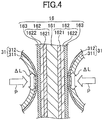
- FIG. 4 schematically illustrates a state in which the male terminal is fitted into the female terminal and used in the circumstance where they are easily subject to vibration.
- the male terminal 16 are pressed by the female terminal 31 at two points from the opposite sides with a contact pressure P. Further, the male terminal 16 and the female terminal 31 are subject to the vibration, which causes the male terminal 16 and the female terminal 31 to relatively slide by a slide distance ⁇ L.
- the wear amount W can be reduced if the contact pressure is decreased. Further, it can be understood that the wear amount W can be reduced if the slide distance ⁇ L is decreased. Further, it can be understood that the wear amount W can be reduced if the Vickers hardness Hv is increased.
- the sliding portion of the male terminal 16 includes the first primary coat 1621 and the second primary coat 1622, and the first primary coat 1621 is less hard than the second primary coat 1622.
- the first primary coat 1621 functions as a stress relieving layer against the contact pressure P, and a probability that the crack of the second primary coat 1622 occurs can be reduced even if the hardness of the second primary coat 1622 is high.
- the hardness of the male terminal 16 is increased due to the second primary coat 1622, and thus the wear amount W can be reduced even in a circumstance that is easily subject to the vibration.
- the wear amount W (slide wear amount) of the metal film 163 of the male terminal 16 can be reduced.
- Fig. 5 is a diagram explaining a warping reduction effect in a base material due to the first primary coat 1621 and the second primary coat 1622.
- the plated layer is easily subject to a tension stress immediately after the plating, as illustrated in Fig. 5 (A) .
- the base material tends to warp in such a direction that the base material is in a convex form toward the upper side, as illustrated in Fig. 5 (A) .
- the electroless NiP plating P: 7% through 13%) is performed for the base material (Cu)
- the plated layer is easily subject to a compression stress, as illustrated in Fig. 5 (B) .
- the base material tends to warp in such a direction that the base material is in a convex form toward the lower side, as illustrated in Fig. 5 (B) .
- the warping of the base material can be reduced, because the tension stress of the Ni electroplating layer and the compression stress of the electroless NiP plating layer act in such a direction that the tension stress of the Ni electroplating layer and the compression stress of the electroless NiP plating layer are canceled, as illustrated in Fig. 5(C) .
- the second primary coat 1622 which is subject to the compression stress, is a primary coat for the metal film 163, a probability that the crack of the metal film 163 occurs can be reduced, even if the thickness of the second primary coat 1622 and thus residual stress are increased or a thermal stress occurs during the manufacturing process. This is because, in general, material strength is substantially higher against the compression than against the tension.
- the electroless NiP plating can be performed using the first primary coat 1621 (Ni electroplating) as a seed layer.
- the manufacturing process can be further simplified.
- Fig. 6 and Fig. 7 are diagrams explaining a way of increasing the hardness of the second primary coat 1622 (electroless NiP plating).
- the hardness of the second primary coat 1622 may be increased by adjusting a heat treatment temperature, as illustrated in Fig. 6 (A) . Further, the hardness of the second primary coat 1622 may be increased by increasing the thickness of the plating, as illustrated in Fig. 6 (B) . Further, the hardness of the second primary coat 1622 may be increased by increasing the heat treatment time, as illustrated in Fig. 7 (A) . Further, the hardness of the second primary coat 1622 may be increased by adjusting the content of P, as illustrated in Fig. 7 (B) .
- the first primary coat 1621 has different hardness with respect to the second primary coat 1622, as is the case with the first embodiment.
- the first primary coat 1621 is harder than the second primary coat 1622.
- the second primary coat 1622 is formed by Ni electroplating, and first primary coat 1621 is formed by electroless NiP plating.
- the hardness of the second primary coat 1622 is preferably in a range between 150 and 500 [HV], and the hardness of the first primary coat 1621 is preferably in a range between 500 and 1000 [HV].
- the second primary coat 1622 functions as a stress relieving layer against the contact pressure P, and a probability that the crack of the first primary coat 1621 occurs can be reduced (and thus the durability can be increased) even if the hardness of the first primary coat 1621 is high. Further, the hardness of the male terminal 16 is increased due to the first primary coat 1621, and thus the wear amount W can be reduced even in a circumstance that is easily subject to the vibration. As a result of this, the wear amount W (slide wear amount) of the metal film 163 of the male terminal 16 can be reduced (and thus the durability can be increased).
- the variant of the first embodiment like the first embodiment, it becomes possible to reduce the warping of the metal material 161 of the male terminal 16, which is a base material, by forming the first primary coat 1621 and the second primary coat 1622.
- the electroless NiP plating is performed for the lead frame as a whole, and then the Ni electroplating and the Au electroplating can be performed successively and partially for only a contact portion on the uppermost surface. It is noted that, in this case, the Au electroplating forms the metal film 163. With this arrangement, the manufacturing process can be further simplified.
- Vickers hardness is used as an index for explaining the difference of the hardness between the objects; however, indexes other than Vickers hardness may be used to show the difference of the hardness between the objects.
- the terminal connection structure according to the embodiment and the variant thereof a certain effect is obtained when it is used in a circumstance that is easily subject to the vibration; however, needless to say, the terminal connection structure according to the embodiment and the variant thereof may be used in circumstances other than the circumstance that is easily subject to the vibration.
Landscapes
- Chemical & Material Sciences (AREA)
- Engineering & Computer Science (AREA)
- Chemical Kinetics & Catalysis (AREA)
- Materials Engineering (AREA)
- Metallurgy (AREA)
- Organic Chemistry (AREA)
- General Chemical & Material Sciences (AREA)
- Mechanical Engineering (AREA)
- Electrochemistry (AREA)
- Electroplating Methods And Accessories (AREA)
- Lead Frames For Integrated Circuits (AREA)
- Microelectronics & Electronic Packaging (AREA)
Abstract
Description
- The disclosure is related to a terminal connection structure, etc.
- A structure is known in which a terminal (male side) for coupling an electronic part to an external device is inserted into a penetrating hole (female side) of a substrate to be coupled to a wiring on the substrate with solder, etc. An example is a semiconductor apparatus in which a terminal for coupling a semiconductor module, which has a semiconductor element covered with resin, to an external device is inserted into a penetrating hole of a substrate to be coupled to a wiring on the substrate with solder, etc., (see,
Patent Document 1, for example). - [Patent Document 1] Japanese Laid-open Patent Publication No.
2010-199622 - According to the technique disclosed in
Patent Document 1, a process for coupling the terminal to the wiring with the solder, etc., is required, which leads to the increased complexity of a manufacturing process. Thus, instead of coupling the terminal to the wiring with the solder, etc., such a terminal connection structure is preferable in which the terminal of the male side and the terminal of the female side are coupled to each other without the solder, etc. In this case, it is useful to appropriately consider durability of a terminal to design a terminal connection structure. - It is an object of the present disclosure to provide a terminal connection structure, etc., that can increase durability of a terminal.
- According to one aspect of the disclosure, a terminal connection structure is provided, which includes: a male terminal; and
a female terminal having an elasticity and configured to have the male terminal fitted therein such that the female terminal sandwiches the male terminal from opposite sides; wherein
the male terminal includes a base material, a first primary coat coated on the base material, a second primary coat coated on the first primary coat, and a surface layer coated on the second primary coat, and
the first primary coat and the second primary coat have different hardnesses. - According to the present disclosure, a terminal connection structure, etc., that can increase durability of a terminal can be obtained.
-
-
Fig. 1 is a diagram illustrating an example of a semiconductor apparatus according to the first embodiment. -
Fig. 2 is a perspective view for illustrating an example of the semiconductor apparatus according to the first embodiment. -
Fig. 3 is a schematic cross-section view of an example of a structure of a portion where a male terminal is fitted into a female terminal. -
Fig. 4 is a schematic cross-section view explaining an increased durability. -
Fig. 5 is a diagram explaining a warping reduction effect in a base material due to a firstprimary coat 1621 and a secondprimary coat 1622. -
Fig. 6 is a diagram explaining a way of increasing hardness of the second primary coat 1622 (electroless NiP plating). -
Fig. 7 is a diagram explaining another way of increasing hardness of the second primary coat 1622 (electroless NiP plating). - In the following, embodiments are described in detail with reference to appended drawings. In the embodiments, as an example of a terminal connection structure, a semiconductor apparatus in which a male terminal, which is a terminal for coupling a semiconductor module to an external device, is fitted into a female terminal, which is disposed in a connector installed on a substrate, is described; however, this is not indispensable. For example, a female terminal, which is a terminal for coupling an electronic part not including a semiconductor element to an external device, may be fitted into a female terminal, which is disposed in a connector installed on a substrate. Further, a male terminal projecting from a first connector installed in a first substrate may be fitted into a female terminal in a second connector installed on a second substrate. It is noted that in the respective drawings, the same elements are indicated by the same reference numerals, and explanation may be omitted to avoid overlaps.
-
Fig. 1 is a diagram illustrating an example of a semiconductor apparatus according to the first embodiment. InFig. 1 , (a) is a perspective view, and (b) is a section-view along a plane through a male terminal 16 (described hereinafter) and parallel to YZ plane of (a). With reference toFig. 1 , asemiconductor apparatus 1 includes asemiconductor module 10, asubstrate 20, and aconnector 30. According to thesemiconductor apparatus 1,male terminals semiconductor module 10 to an external device(s), are fitted intofemale terminals 31 in theconnector 30 via thesubstrate 20. - In the following, the
semiconductor apparatus 1 is described in detail. At first, thesemiconductor module 10, thesubstrate 20, and theconnector 30 are simply described, and then a structure (i.e., a terminal connection structure) of a portion where themale terminals semiconductor module 10 are fitted into thefemale terminals 31 of theconnector 30 is described in detail. - At first, the
semiconductor module 10 is described. Thesemiconductor module 10 may have any internal structure, as long as thesemiconductor module 10 includes a male terminal for an external connection. In the present embodiment, as an example, an semiconductor module including IGBTs (Insulated gate bipolar transistors) and diodes is described. -
Fig. 2 is a perspective view for illustrating an example of the semiconductor apparatus according to the first embodiment. With referenceFig. 1 andFig. 2 , thesemiconductor module 10 includes ametal plate 11, ametal plate 12, ametal plate 14, ametal plate 15, a plurality ofmale terminals 16, a plurality ofmale terminals 17, and asealing resin 18. - In the
semiconductor module 10, first semiconductor elements (not illustrated) are installed such that the first semiconductor elements are sandwiched between themetal plates metal plates - The
metal plates metal plates 11 through 15 can radiate heat, which is generated due to operations of the first and second semiconductor elements, to the outside. - The
metal plates 11 through 15 may be formed of a copper (Cu), an aluminum (Al), etc., for example. The surfaces of themetal plates 11 through 15 may be plated. Themetal plates 11 through 15 may be formed of lead frames, for example. - The first semiconductor elements include IGBTs, and reflux diodes coupled between emitters and collectors of the IGBTs, which are a part of an inverter circuit or a booster converter circuit installed on a vehicle, for example. The second semiconductors element are the same as the first semiconductor elements.
- The
male terminals 16 are metal terminals for external connection of thesemiconductor module 10. Themale terminals 16 are electrically coupled to the first semiconductor elements, a temperature sensor, etc., via bonding wires, for example. Themale terminals 17 are metal terminals for external connection of thesemiconductor module 10. Themale terminals 16 are electrically coupled to the second semiconductor elements, a temperature sensor, etc., via bonding wires, for example. - The
metal plates 11 through 15,male terminals resin 18. However, ends of themetal plates 11 through 13 are projected out of the sealingresin 18. Further, predetermined surfaces of themetal plates resin 18. Further, ends of themetal plates resin 18. It is noted that the ends of themetal plates 11 through 13, and the ends of themale terminals sealing resin 18 may be formed from an epoxy-based resin having a filler therein, for example. - With reference to
Fig. 1 , thesubstrate 20 is a part on which thesemiconductor module 10 is installed. Thesubstrate 20 may include a circuit (not illustrated) for driving thesemiconductor module 10. Thesubstrate 20 may be a so-called glass epoxy substrate in which glass cloth is impregnated with insulating resin such as epoxy-based resin, etc., a silicon substrate, a ceramic substrate, etc. Thesubstrate 20 may include multilayered wiring layers. - The
substrate 20 has a plurality of penetratingportions 20x formed therein through which themale terminals semiconductor module 10 are inserted. The shape of the penetratingportions 20x in a plan view corresponds to a sectional shape of themale terminals male terminals surface 20a of thesubstrate 20. - The penetrating
portions 20x in a plan view are formed such that the size is greater than the sectional size of themale terminals male terminals male terminals portions 20x. Thus, there are clearances between the internal walls of the penetratingportions 20x and the side surfaces of themale terminals portions 20x may be holes, cutouts, etc., penetrating thesubstrate 20. - The
connector 30 is installed on thesurface 20a of thesubstrate 20. Theconnector 30 includes thefemale terminals 31 whose number corresponds to the number of themale terminals female terminals 31 can be electrically coupled to the circuit formed on thesubstrate 20. - The
male terminals semiconductor module 10 are inserted to be fitted into thefemale terminals 31 of theconnector 30 from the side of asurface 20b opposite to thesurface 20a of thesubstrate 20. With this arrangement, the first and second semiconductor elements of thesemiconductor module 10 can be electrically coupled to the wirings (circuit) formed on thesubstrate 20 via themale terminals female terminals 31 of theconnector 30. - It is noted that in the semiconductor apparatus 1 a
single semiconductor module 10 is fitted into theconnector 30 via thesubstrate 20; however, a plurality ofsemiconductor modules 10 may be fitted intocorresponding connectors 30 via thesubstrate 20. - Next, a structure (i.e., a terminal connection structure) of a portion where the
male terminals semiconductor module 10 are fitted into thefemale terminals 31 of theconnector 30 is described in detail.Fig. 3 is a schematic cross-section view of an example of a structure of a portion where a male terminal is fitted into a female terminal, and illustrates an enlarged part of the section-view inFig. 1 (b) . It is noted that the illustration of thefemale terminals 17 is omitted, but thefemale terminals 17 have the same structures as themale terminals 16. - With reference
Fig. 3 , themale terminal 16 includes ametal material 161, which is a base material formed on a center side, ametal film 162 coated on themetal material 161, and ametal film 163, which is coated on themetal film 162 and is a surface treating material formed on an uppermost surface of themale terminal 16. It is noted that a base material is a portion functioning as a base for forming the surface treating material, etc. - For the
metal material 161, a metal plate whose main component is a copper (Cu), a copper alloy, aluminum (Al), an aluminum alloy, etc., can be used. The thickness of themetal plate 161 may be 0.2 to 0.8 millimeters, for example. It is noted that the main component is a component whose proportion (weight %) in the member in question is the greatest, if a plurality of metal materials are included in the member in question or an additive, etc., is included in the member in question. - The
metal film 162 includes a firstprimary coat 1621 coated on themetal material 161 and a secondprimary coat 1622 coated on the firstprimary coat 1621. Thus, themetal film 163 is coated on the secondprimary coat 1622. It is noted that themetal film 162 may further include one or more layers in addition to the firstprimary coat 1621 and the secondprimary coat 1622. - The first
primary coat 1621 has a different hardness (Vickers hardness) with respect to the secondprimary coat 1622. Specifically, the secondprimary coat 1622 is harder than the firstprimary coat 1621. The firstprimary coat 1621 is formed by Ni electroplating, and the secondprimary coat 1622 is formed by NiP electroless plating. The hardness of the firstprimary coat 1621 is preferably in a range between 150 and 500 [HV], and the hardness of the secondprimary coat 1622 is preferably in a range between 500 and 1000 [HV]. - It is noted that according to the present embodiment, the first
primary coat 1621 and the secondprimary coat 1622 are formed of Ni and NiP, respectively; however, other materials may be used. For example, tin (Sn), copper (Cu), silver (Ag), lead (Pb), zinc (Zn), phosphorus (P), boron (B), chrome (Cr), manganese (Mn), iron (Fe), cobalt (Co), palladium (Pd), platinum (Pt), titanium (Ti), zirconium (Zr), vanadium (V), molybdenum (Mo), tungsten (W), indium (In), antimony (Sb), bismuth (Bi), etc., may be used, and a composite such as nickel-boron (NiB), etc., may be used. - For the
metal film 163, a metal film whose main component is a noble metal such as gold (Au), platinum (Pt), palladium (Pd), rhodium (Rh), etc., can be used. The thickness of themetal plate 163 may be 0.3 to 0.8 micrometers, for example. Themetal film 163 can be formed on themetal film 162 by plating, for example. - The
female terminal 31 includes ametal material 311, which is a base material, and ametal film 312, which is coated on themetal material 311 and is a surface treating material formed on an uppermost surface of thefemale terminal 31. - The
female terminal 31 has elasticity. Thefemale terminal 31 has the same structure on opposite sides with respect to themale terminal 16, and uses the elasticity to press the male terminal 16 from the opposite sides. Themetal film 312 of thefemale terminal 31 comes into contact with themetal film 163 of themale terminal 16. - In a state before the insertion of the
male terminal 16, thefemale terminal 31 has two portions opposed to each other such that themetal films 312 of the portions face inwardly (i.e., to the side to come into contact with the male terminal 16) with such a space that enables themale terminal 16 to be inserted therebetween and pressed from the opposite sides by the elasticity thereof. It is noted that the portions of thefemale terminal 31 on the opposite sides of themale terminal 16 are integrated in theconnector 30 to be electrically coupled to each other. - For the
metal material 311, a metal plate whose main component is a copper (Cu), a copper alloy, an aluminum (Al), an aluminum alloy, etc., can be used. The thickness of themetal plate 311 may be 0.1 to 0.3 millimeters, for example. It is noted that themetal material 311, which is a base material of thefemale terminal 31, may have the same or different hardness with respect to themetal material 161, which is a base material of themale terminal 16. For example, the hardness of themetal material 311 and themetal material 161 may be in a range between 40 and 200 [HV]. - For the
metal film 312, a metal film whose main component is a noble metal such as gold (Au), platinum (Pt), palladium (Pd), rhodium (Rh), etc., can be used. The thickness of themetal plate 312 may be 0.3 to 0.8 micrometers, for example. Themetal film 312 can be formed on themetal material 311 by plating, for example. The hardness of themetal film 312 is arbitrary; however, the hardness of themetal film 312 may be the same as that of themetal film 163, for example. - It is noted that the
female terminal 31 may include a metal film sandwiched between themetal material 311 and themetal film 312. The material and the thickness of the metal film sandwiched between themetal material 311 and themetal film 312 are arbitrary. - According to the embodiment, as described above, because the first
primary coat 1621 and the secondprimary coat 1622 of themetal film 162 of themale terminal 16 have different hardnesses, durability of themale terminal 16 can be increased even if thesemiconductor apparatus 1 is used under a circumstance where thesemiconductor apparatus 1 is easily subject to vibration. It is noted that the circumstance where thesemiconductor apparatus 1 is easily subject to vibration is such a case where thesemiconductor apparatus 1 is installed on a moving object, etc., for example. The moving object is an automobile, a motorcycle, a train, etc., for example. - Here, with respect to
Fig. 4 , the effect of increasing the durability is further described.Fig. 4 schematically illustrates a state in which the male terminal is fitted into the female terminal and used in the circumstance where they are easily subject to vibration. InFig. 4 , themale terminal 16 are pressed by thefemale terminal 31 at two points from the opposite sides with a contact pressure P. Further, themale terminal 16 and thefemale terminal 31 are subject to the vibration, which causes themale terminal 16 and thefemale terminal 31 to relatively slide by a slide distance ΔL. - In this case, when it is assumed that a wear amount is W, a coefficient of friction is K, and Vickers hardness is Hv, a relationship expressed by a formula (1) is held. It is noted that the coefficient of friction K is determined depending on surface roughness of the
metal film 163 of themale terminal 16, surface roughness of themetal film 312 of thefemale terminal 31, a contact area therebetween, etc.
[Math. 1]
- From the formula (1), it can be understood that the wear amount W can be reduced if the contact pressure is decreased. Further, it can be understood that the wear amount W can be reduced if the slide distance ΔL is decreased. Further, it can be understood that the wear amount W can be reduced if the Vickers hardness Hv is increased.
- According to a configuration in which the hardness is merely increased at the sliding portion of the male terminal 16 (for example, a configuration where the first
primary coat 1621 is not provided), there is a problem that a crack of the second primary coat 1622 (NiP electroless plating) easily occurs, even though the wear amount W can be reduced. On the other hand, according to a configuration in which the hardness is decreased at the sliding portion of the male terminal 16 (for example, a configuration where the secondprimary coat 1622 is not provided), themetal film 163 at the uppermost surface, etc., is easily to be worn due to the reduction in the hardness of the slide portion of themale terminal 16, even though the crack can be prevented. - Regarding this point, according to the embodiment, as described above, the sliding portion of the
male terminal 16 includes the firstprimary coat 1621 and the secondprimary coat 1622, and the firstprimary coat 1621 is less hard than the secondprimary coat 1622. Thus, the firstprimary coat 1621 functions as a stress relieving layer against the contact pressure P, and a probability that the crack of the secondprimary coat 1622 occurs can be reduced even if the hardness of the secondprimary coat 1622 is high. Further, the hardness of themale terminal 16 is increased due to the secondprimary coat 1622, and thus the wear amount W can be reduced even in a circumstance that is easily subject to the vibration. As a result of this, the wear amount W (slide wear amount) of themetal film 163 of themale terminal 16 can be reduced. Thus, according to the embodiment, it becomes possible to keep the contact pressure P with respect to thefemale terminal 31 greater than or equal to a certain value, while increasing the durability of themale terminal 16. -
Fig. 5 is a diagram explaining a warping reduction effect in a base material due to the firstprimary coat 1621 and the secondprimary coat 1622. - If the Ni electroplating is performed for the base material (Cu), the plated layer is easily subject to a tension stress immediately after the plating, as illustrated in
Fig. 5 (A) . In this case, the base material tends to warp in such a direction that the base material is in a convex form toward the upper side, as illustrated inFig. 5 (A) . Further, if the electroless NiP plating (P: 7% through 13%) is performed for the base material (Cu), the plated layer is easily subject to a compression stress, as illustrated inFig. 5 (B) . In this case, the base material tends to warp in such a direction that the base material is in a convex form toward the lower side, as illustrated inFig. 5 (B) . - On the other hand, if the Ni electroplating and the electroless NiP plating are performed for the base material (Cu), the warping of the base material can be reduced, because the tension stress of the Ni electroplating layer and the compression stress of the electroless NiP plating layer act in such a direction that the tension stress of the Ni electroplating layer and the compression stress of the electroless NiP plating layer are canceled, as illustrated in
Fig. 5(C) . Thus, according to the embodiment, it becomes possible to reduce the warping of themetal material 161 of themale terminal 16, which is a base material, by forming the firstprimary coat 1621 and the secondprimary coat 1622. - Further, according to the embodiment, because the second
primary coat 1622, which is subject to the compression stress, is a primary coat for themetal film 163, a probability that the crack of themetal film 163 occurs can be reduced, even if the thickness of the secondprimary coat 1622 and thus residual stress are increased or a thermal stress occurs during the manufacturing process. This is because, in general, material strength is substantially higher against the compression than against the tension. - Further, according to the embodiment, the electroless NiP plating can be performed using the first primary coat 1621 (Ni electroplating) as a seed layer. With this arrangement, the manufacturing process can be further simplified.
-
Fig. 6 andFig. 7 are diagrams explaining a way of increasing the hardness of the second primary coat 1622 (electroless NiP plating). - The hardness of the second primary coat 1622 (electroless NiP plating) may be increased by adjusting a heat treatment temperature, as illustrated in
Fig. 6 (A) . Further, the hardness of the secondprimary coat 1622 may be increased by increasing the thickness of the plating, as illustrated inFig. 6 (B) . Further, the hardness of the secondprimary coat 1622 may be increased by increasing the heat treatment time, as illustrated inFig. 7 (A) . Further, the hardness of the secondprimary coat 1622 may be increased by adjusting the content of P, as illustrated inFig. 7 (B) . - According to a variant of the first embodiment, the first
primary coat 1621 has different hardness with respect to the secondprimary coat 1622, as is the case with the first embodiment. However, according to the variant of the first embodiment, unlike the first embodiment, the firstprimary coat 1621 is harder than the secondprimary coat 1622. The secondprimary coat 1622 is formed by Ni electroplating, and firstprimary coat 1621 is formed by electroless NiP plating. The hardness of the secondprimary coat 1622 is preferably in a range between 150 and 500 [HV], and the hardness of the firstprimary coat 1621 is preferably in a range between 500 and 1000 [HV]. - Again, according to the variant of the first embodiment, like the first embodiment, the second
primary coat 1622 functions as a stress relieving layer against the contact pressure P, and a probability that the crack of the firstprimary coat 1621 occurs can be reduced (and thus the durability can be increased) even if the hardness of the firstprimary coat 1621 is high. Further, the hardness of themale terminal 16 is increased due to the firstprimary coat 1621, and thus the wear amount W can be reduced even in a circumstance that is easily subject to the vibration. As a result of this, the wear amount W (slide wear amount) of themetal film 163 of themale terminal 16 can be reduced (and thus the durability can be increased). - Further, according to the variant of the first embodiment, like the first embodiment, it becomes possible to reduce the warping of the
metal material 161 of themale terminal 16, which is a base material, by forming the firstprimary coat 1621 and the secondprimary coat 1622. - Further, according to the variant of the first embodiment, the electroless NiP plating is performed for the lead frame as a whole, and then the Ni electroplating and the Au electroplating can be performed successively and partially for only a contact portion on the uppermost surface. It is noted that, in this case, the Au electroplating forms the
metal film 163. With this arrangement, the manufacturing process can be further simplified. - All examples and conditional language recited herein are intended for pedagogical purposes to aid the reader in understanding the invention and the concepts contributed by the inventor to furthering the art, and are to be construed as being without limitation to such specifically recited examples and conditions, nor does the organization of such examples in the specification relate to a showing of the superiority and inferiority of the invention. Although the embodiment(s) of the present inventions have been described in detail, it should be understood that the various changes, substitutions, and alterations could be made hereto without departing from the spirit and scope of the invention. Further, all or part of the components of the embodiments described above can be combined.
- For example, according to the embodiment and the variant thereof, Vickers hardness is used as an index for explaining the difference of the hardness between the objects; however, indexes other than Vickers hardness may be used to show the difference of the hardness between the objects.
- Further, the terminal connection structure according to the embodiment and the variant thereof, a certain effect is obtained when it is used in a circumstance that is easily subject to the vibration; however, needless to say, the terminal connection structure according to the embodiment and the variant thereof may be used in circumstances other than the circumstance that is easily subject to the vibration.
- The present international application is based on Japanese Priority Application No.
2014-046594, filed on March 10, 2014 -
- 1
- semiconductor apparatus
- 10
- semiconductor module
- 11, 12, 13, 14, 15
- metal plate
- 16
- male terminal
- 18
- sealing resin
- 20
- substrate
- 30
- connector
- 31
- female terminal
- 161, 311
- metal material
- 162
- metal film
- 1621
- first primary coat
- 1622
- second primary coat
- 163, 312
- metal film
- P
- contact pressure
- ΔL
- slide distance
Claims (6)
- A terminal connection structure, comprising:a male terminal; anda female terminal having an elasticity and configured to have the male terminal fitted therein such that the female terminal sandwiches the male terminal from opposite sides; whereinthe male terminal includes a base material, a first primary coat coated on the base material, a second primary coat coated on the first primary coat, and a surface layer coated on the second primary coat, and
the first primary coat and the second primary coat have different hardness. - The terminal connection structure of claim 1, wherein the first primary coat is harder than the second primary coat.
- The terminal connection structure of claim 2, wherein the first primary coat is an electroless plating layer, and the second primary coat is an electroplating layer.
- The terminal connection structure of claim 1, wherein the second primary coat is harder than the first primary coat.
- The terminal connection structure of claim 4, wherein the second primary coat is an electroless plating layer, and the first primary coat is an electroplating layer.
- A semiconductor apparatus including the terminal connection structure of any one of claims 1 through 5, wherein
the male terminal is a terminal for coupling a semiconductor module to an external device, and
the female terminal is a terminal in a connector installed on a substrate.
Applications Claiming Priority (2)
| Application Number | Priority Date | Filing Date | Title |
|---|---|---|---|
| JP2014046594A JP6181581B2 (en) | 2014-03-10 | 2014-03-10 | Terminal connection structure, semiconductor device |
| PCT/JP2015/051227 WO2015136984A1 (en) | 2014-03-10 | 2015-01-19 | Terminal connection structure and semiconductor device |
Publications (3)
| Publication Number | Publication Date |
|---|---|
| EP3118937A1 true EP3118937A1 (en) | 2017-01-18 |
| EP3118937A4 EP3118937A4 (en) | 2017-05-17 |
| EP3118937B1 EP3118937B1 (en) | 2019-11-27 |
Family
ID=54071438
Family Applications (1)
| Application Number | Title | Priority Date | Filing Date |
|---|---|---|---|
| EP15760655.9A Active EP3118937B1 (en) | 2014-03-10 | 2015-01-19 | Terminal connection structure and semiconductor apparatus |
Country Status (7)
| Country | Link |
|---|---|
| US (1) | US9711884B2 (en) |
| EP (1) | EP3118937B1 (en) |
| JP (1) | JP6181581B2 (en) |
| KR (1) | KR101805339B1 (en) |
| CN (1) | CN106165202B (en) |
| TW (1) | TWI542084B (en) |
| WO (1) | WO2015136984A1 (en) |
Families Citing this family (4)
| Publication number | Priority date | Publication date | Assignee | Title |
|---|---|---|---|---|
| JP6676935B2 (en) | 2015-11-13 | 2020-04-08 | セイコーエプソン株式会社 | Electric devices, piezoelectric motors, robots, hands and liquid pumps |
| JP2020187971A (en) * | 2019-05-16 | 2020-11-19 | 株式会社オートネットワーク技術研究所 | Connector terminals, wires with terminals, and terminal pairs |
| JP2024033060A (en) * | 2022-08-30 | 2024-03-13 | モレックス エルエルシー | Connectors and connector pairs |
| JP2026060075A (en) * | 2024-09-27 | 2026-04-08 | 株式会社ヨコオ | Metal materials, contact terminals and connectors |
Family Cites Families (15)
| Publication number | Priority date | Publication date | Assignee | Title |
|---|---|---|---|---|
| US2537370A (en) * | 1948-10-12 | 1951-01-09 | Abraham D Parnes | Male safety plug member |
| US4169646A (en) * | 1977-11-14 | 1979-10-02 | Amp Incorporated | Insulated contact |
| JP2000087291A (en) * | 1998-09-17 | 2000-03-28 | Furukawa Electric Co Ltd:The | Aluminum-based composite base plate for electronic device and method of manufacturing the same |
| US6335107B1 (en) * | 1999-09-23 | 2002-01-01 | Lucent Technologies Inc. | Metal article coated with multilayer surface finish for porosity reduction |
| JP4514012B2 (en) * | 2001-01-19 | 2010-07-28 | 古河電気工業株式会社 | Plating material, manufacturing method thereof, and electric / electronic parts using the same |
| JP4302392B2 (en) | 2002-11-28 | 2009-07-22 | 三菱伸銅株式会社 | Connector terminal, connector, connector terminal manufacturing method, and connector strip |
| JP2004297972A (en) * | 2003-03-28 | 2004-10-21 | Toyota Industries Corp | Semiconductor device |
| JP4302545B2 (en) | 2004-02-10 | 2009-07-29 | 株式会社オートネットワーク技術研究所 | Press-fit terminal |
| JP2006108057A (en) | 2004-10-08 | 2006-04-20 | Matsushita Electric Works Ltd | Connector joint terminal |
| JP2008108675A (en) * | 2006-10-27 | 2008-05-08 | Toshiba Corp | plug |
| JP5151950B2 (en) * | 2008-12-11 | 2013-02-27 | 三菱マテリアル株式会社 | Sn plating material and manufacturing method thereof |
| JP5385683B2 (en) * | 2009-05-22 | 2014-01-08 | 矢崎総業株式会社 | Connector terminal |
| CN102405561B (en) * | 2009-09-08 | 2014-04-30 | 矢崎总业株式会社 | Terminal fitting and method for assembling said terminal fitting |
| JP5363300B2 (en) * | 2009-12-24 | 2013-12-11 | エスペック株式会社 | socket |
| JP5511515B2 (en) | 2010-05-31 | 2014-06-04 | 株式会社日立製作所 | Power converter |
-
2014
- 2014-03-10 JP JP2014046594A patent/JP6181581B2/en active Active
-
2015
- 2015-01-19 WO PCT/JP2015/051227 patent/WO2015136984A1/en not_active Ceased
- 2015-01-19 CN CN201580012762.6A patent/CN106165202B/en active Active
- 2015-01-19 KR KR1020167024015A patent/KR101805339B1/en active Active
- 2015-01-19 US US15/123,145 patent/US9711884B2/en active Active
- 2015-01-19 EP EP15760655.9A patent/EP3118937B1/en active Active
- 2015-02-02 TW TW104103428A patent/TWI542084B/en active
Also Published As
| Publication number | Publication date |
|---|---|
| US9711884B2 (en) | 2017-07-18 |
| JP6181581B2 (en) | 2017-08-16 |
| KR20160114714A (en) | 2016-10-05 |
| US20170110819A1 (en) | 2017-04-20 |
| EP3118937B1 (en) | 2019-11-27 |
| CN106165202A (en) | 2016-11-23 |
| JP2015170570A (en) | 2015-09-28 |
| WO2015136984A1 (en) | 2015-09-17 |
| TW201603397A (en) | 2016-01-16 |
| EP3118937A4 (en) | 2017-05-17 |
| TWI542084B (en) | 2016-07-11 |
| CN106165202B (en) | 2019-05-28 |
| KR101805339B1 (en) | 2017-12-05 |
Similar Documents
| Publication | Publication Date | Title |
|---|---|---|
| EP3118937B1 (en) | Terminal connection structure and semiconductor apparatus | |
| AU2017248560B2 (en) | Semiconductor device and manufacturing method for the semiconductor device | |
| US9013034B2 (en) | Semiconductor package | |
| US10886203B2 (en) | Packaging structure with recessed outer and inner lead surfaces | |
| US10727169B2 (en) | Semiconductor device having lead with back and end surfaces provided with plating layers | |
| US20070057373A1 (en) | Semiconductor device having metallic plate with groove | |
| US20190279943A1 (en) | Power semiconductor device | |
| US12354981B2 (en) | Semiconductor device and method for manufacturing the same | |
| US20140203253A1 (en) | Organic Light Emitting Diode, Method for Producing an Organic Light Emitting Diode and Module Comprising at Least Two Organic Light Emitting Diodes | |
| US11133276B2 (en) | Semiconductor device and method for manufacturing the same | |
| US10014237B2 (en) | Circuit board having a heat dissipating sheet with varying metal grain size | |
| US20160322726A1 (en) | Terminal connecting structure and semiconductor device | |
| US20090051022A1 (en) | Lead frame structure | |
| JP4503046B2 (en) | Manufacturing method of semiconductor device | |
| JP6834815B2 (en) | Semiconductor module | |
| CN108293298A (en) | Automotive electronic modules, card edge connectors and connectors | |
| US20240234359A9 (en) | Semiconductor Device and Manufacturing Method for Semiconductor Device | |
| JP5744447B2 (en) | Lead frame manufacturing method and lead frame | |
| US20220149260A1 (en) | Thermoelectric conversion module |
Legal Events
| Date | Code | Title | Description |
|---|---|---|---|
| STAA | Information on the status of an ep patent application or granted ep patent |
Free format text: STATUS: THE INTERNATIONAL PUBLICATION HAS BEEN MADE |
|
| PUAI | Public reference made under article 153(3) epc to a published international application that has entered the european phase |
Free format text: ORIGINAL CODE: 0009012 |
|
| STAA | Information on the status of an ep patent application or granted ep patent |
Free format text: STATUS: REQUEST FOR EXAMINATION WAS MADE |
|
| 17P | Request for examination filed |
Effective date: 20161003 |
|
| AK | Designated contracting states |
Kind code of ref document: A1 Designated state(s): AL AT BE BG CH CY CZ DE DK EE ES FI FR GB GR HR HU IE IS IT LI LT LU LV MC MK MT NL NO PL PT RO RS SE SI SK SM TR |
|
| AX | Request for extension of the european patent |
Extension state: BA ME |
|
| RAP1 | Party data changed (applicant data changed or rights of an application transferred) |
Owner name: TOYOTA JIDOSHA KABUSHIKI KAISHA |
|
| A4 | Supplementary search report drawn up and despatched |
Effective date: 20170420 |
|
| RIC1 | Information provided on ipc code assigned before grant |
Ipc: H01L 23/50 20060101ALI20170412BHEP Ipc: H01R 13/03 20060101AFI20170412BHEP Ipc: H01L 25/07 20060101ALI20170412BHEP Ipc: H01L 25/18 20060101ALI20170412BHEP Ipc: C23C 18/54 20060101ALI20170412BHEP Ipc: H01R 13/11 20060101ALI20170412BHEP Ipc: H01R 12/77 20110101ALI20170412BHEP Ipc: H01R 12/71 20110101ALI20170412BHEP Ipc: H01R 12/70 20110101ALI20170412BHEP |
|
| DAX | Request for extension of the european patent (deleted) | ||
| RIC1 | Information provided on ipc code assigned before grant |
Ipc: H01L 23/50 20060101ALI20190408BHEP Ipc: H01R 13/03 20060101AFI20190408BHEP Ipc: H01R 12/70 20110101ALI20190408BHEP Ipc: H01L 25/07 20060101ALI20190408BHEP Ipc: H01R 13/11 20060101ALI20190408BHEP Ipc: H01R 12/71 20110101ALI20190408BHEP Ipc: C23C 18/54 20060101ALI20190408BHEP Ipc: H01L 25/18 20060101ALI20190408BHEP Ipc: H01R 12/77 20110101ALI20190408BHEP |
|
| GRAP | Despatch of communication of intention to grant a patent |
Free format text: ORIGINAL CODE: EPIDOSNIGR1 |
|
| STAA | Information on the status of an ep patent application or granted ep patent |
Free format text: STATUS: GRANT OF PATENT IS INTENDED |
|
| INTG | Intention to grant announced |
Effective date: 20190522 |
|
| GRAJ | Information related to disapproval of communication of intention to grant by the applicant or resumption of examination proceedings by the epo deleted |
Free format text: ORIGINAL CODE: EPIDOSDIGR1 |
|
| STAA | Information on the status of an ep patent application or granted ep patent |
Free format text: STATUS: REQUEST FOR EXAMINATION WAS MADE |
|
| GRAS | Grant fee paid |
Free format text: ORIGINAL CODE: EPIDOSNIGR3 |
|
| STAA | Information on the status of an ep patent application or granted ep patent |
Free format text: STATUS: GRANT OF PATENT IS INTENDED |
|
| GRAP | Despatch of communication of intention to grant a patent |
Free format text: ORIGINAL CODE: EPIDOSNIGR1 |
|
| INTC | Intention to grant announced (deleted) | ||
| GRAA | (expected) grant |
Free format text: ORIGINAL CODE: 0009210 |
|
| STAA | Information on the status of an ep patent application or granted ep patent |
Free format text: STATUS: THE PATENT HAS BEEN GRANTED |
|
| INTG | Intention to grant announced |
Effective date: 20190930 |
|
| AK | Designated contracting states |
Kind code of ref document: B1 Designated state(s): AL AT BE BG CH CY CZ DE DK EE ES FI FR GB GR HR HU IE IS IT LI LT LU LV MC MK MT NL NO PL PT RO RS SE SI SK SM TR |
|
| REG | Reference to a national code |
Ref country code: GB Ref legal event code: FG4D |
|
| REG | Reference to a national code |
Ref country code: CH Ref legal event code: EP |
|
| REG | Reference to a national code |
Ref country code: DE Ref legal event code: R096 Ref document number: 602015042545 Country of ref document: DE |
|
| REG | Reference to a national code |
Ref country code: AT Ref legal event code: REF Ref document number: 1207774 Country of ref document: AT Kind code of ref document: T Effective date: 20191215 |
|
| REG | Reference to a national code |
Ref country code: IE Ref legal event code: FG4D |
|
| REG | Reference to a national code |
Ref country code: NL Ref legal event code: MP Effective date: 20191127 |
|
| REG | Reference to a national code |
Ref country code: LT Ref legal event code: MG4D |
|
| PG25 | Lapsed in a contracting state [announced via postgrant information from national office to epo] |
Ref country code: FI Free format text: LAPSE BECAUSE OF FAILURE TO SUBMIT A TRANSLATION OF THE DESCRIPTION OR TO PAY THE FEE WITHIN THE PRESCRIBED TIME-LIMIT Effective date: 20191127 Ref country code: BG Free format text: LAPSE BECAUSE OF FAILURE TO SUBMIT A TRANSLATION OF THE DESCRIPTION OR TO PAY THE FEE WITHIN THE PRESCRIBED TIME-LIMIT Effective date: 20200227 Ref country code: LV Free format text: LAPSE BECAUSE OF FAILURE TO SUBMIT A TRANSLATION OF THE DESCRIPTION OR TO PAY THE FEE WITHIN THE PRESCRIBED TIME-LIMIT Effective date: 20191127 Ref country code: SE Free format text: LAPSE BECAUSE OF FAILURE TO SUBMIT A TRANSLATION OF THE DESCRIPTION OR TO PAY THE FEE WITHIN THE PRESCRIBED TIME-LIMIT Effective date: 20191127 Ref country code: LT Free format text: LAPSE BECAUSE OF FAILURE TO SUBMIT A TRANSLATION OF THE DESCRIPTION OR TO PAY THE FEE WITHIN THE PRESCRIBED TIME-LIMIT Effective date: 20191127 Ref country code: NO Free format text: LAPSE BECAUSE OF FAILURE TO SUBMIT A TRANSLATION OF THE DESCRIPTION OR TO PAY THE FEE WITHIN THE PRESCRIBED TIME-LIMIT Effective date: 20200227 Ref country code: GR Free format text: LAPSE BECAUSE OF FAILURE TO SUBMIT A TRANSLATION OF THE DESCRIPTION OR TO PAY THE FEE WITHIN THE PRESCRIBED TIME-LIMIT Effective date: 20200228 Ref country code: NL Free format text: LAPSE BECAUSE OF FAILURE TO SUBMIT A TRANSLATION OF THE DESCRIPTION OR TO PAY THE FEE WITHIN THE PRESCRIBED TIME-LIMIT Effective date: 20191127 |
|
| PG25 | Lapsed in a contracting state [announced via postgrant information from national office to epo] |
Ref country code: HR Free format text: LAPSE BECAUSE OF FAILURE TO SUBMIT A TRANSLATION OF THE DESCRIPTION OR TO PAY THE FEE WITHIN THE PRESCRIBED TIME-LIMIT Effective date: 20191127 Ref country code: IS Free format text: LAPSE BECAUSE OF FAILURE TO SUBMIT A TRANSLATION OF THE DESCRIPTION OR TO PAY THE FEE WITHIN THE PRESCRIBED TIME-LIMIT Effective date: 20200327 Ref country code: RS Free format text: LAPSE BECAUSE OF FAILURE TO SUBMIT A TRANSLATION OF THE DESCRIPTION OR TO PAY THE FEE WITHIN THE PRESCRIBED TIME-LIMIT Effective date: 20191127 |
|
| PG25 | Lapsed in a contracting state [announced via postgrant information from national office to epo] |
Ref country code: AL Free format text: LAPSE BECAUSE OF FAILURE TO SUBMIT A TRANSLATION OF THE DESCRIPTION OR TO PAY THE FEE WITHIN THE PRESCRIBED TIME-LIMIT Effective date: 20191127 |
|
| PG25 | Lapsed in a contracting state [announced via postgrant information from national office to epo] |
Ref country code: EE Free format text: LAPSE BECAUSE OF FAILURE TO SUBMIT A TRANSLATION OF THE DESCRIPTION OR TO PAY THE FEE WITHIN THE PRESCRIBED TIME-LIMIT Effective date: 20191127 Ref country code: PT Free format text: LAPSE BECAUSE OF FAILURE TO SUBMIT A TRANSLATION OF THE DESCRIPTION OR TO PAY THE FEE WITHIN THE PRESCRIBED TIME-LIMIT Effective date: 20200419 Ref country code: DK Free format text: LAPSE BECAUSE OF FAILURE TO SUBMIT A TRANSLATION OF THE DESCRIPTION OR TO PAY THE FEE WITHIN THE PRESCRIBED TIME-LIMIT Effective date: 20191127 Ref country code: RO Free format text: LAPSE BECAUSE OF FAILURE TO SUBMIT A TRANSLATION OF THE DESCRIPTION OR TO PAY THE FEE WITHIN THE PRESCRIBED TIME-LIMIT Effective date: 20191127 Ref country code: CZ Free format text: LAPSE BECAUSE OF FAILURE TO SUBMIT A TRANSLATION OF THE DESCRIPTION OR TO PAY THE FEE WITHIN THE PRESCRIBED TIME-LIMIT Effective date: 20191127 Ref country code: ES Free format text: LAPSE BECAUSE OF FAILURE TO SUBMIT A TRANSLATION OF THE DESCRIPTION OR TO PAY THE FEE WITHIN THE PRESCRIBED TIME-LIMIT Effective date: 20191127 |
|
| REG | Reference to a national code |
Ref country code: DE Ref legal event code: R097 Ref document number: 602015042545 Country of ref document: DE |
|
| PG25 | Lapsed in a contracting state [announced via postgrant information from national office to epo] |
Ref country code: SM Free format text: LAPSE BECAUSE OF FAILURE TO SUBMIT A TRANSLATION OF THE DESCRIPTION OR TO PAY THE FEE WITHIN THE PRESCRIBED TIME-LIMIT Effective date: 20191127 Ref country code: SK Free format text: LAPSE BECAUSE OF FAILURE TO SUBMIT A TRANSLATION OF THE DESCRIPTION OR TO PAY THE FEE WITHIN THE PRESCRIBED TIME-LIMIT Effective date: 20191127 Ref country code: MC Free format text: LAPSE BECAUSE OF FAILURE TO SUBMIT A TRANSLATION OF THE DESCRIPTION OR TO PAY THE FEE WITHIN THE PRESCRIBED TIME-LIMIT Effective date: 20191127 |
|
| REG | Reference to a national code |
Ref country code: CH Ref legal event code: PL |
|
| REG | Reference to a national code |
Ref country code: AT Ref legal event code: MK05 Ref document number: 1207774 Country of ref document: AT Kind code of ref document: T Effective date: 20191127 |
|
| PLBE | No opposition filed within time limit |
Free format text: ORIGINAL CODE: 0009261 |
|
| STAA | Information on the status of an ep patent application or granted ep patent |
Free format text: STATUS: NO OPPOSITION FILED WITHIN TIME LIMIT |
|
| REG | Reference to a national code |
Ref country code: BE Ref legal event code: MM Effective date: 20200131 |
|
| GBPC | Gb: european patent ceased through non-payment of renewal fee |
Effective date: 20200227 |
|
| PG25 | Lapsed in a contracting state [announced via postgrant information from national office to epo] |
Ref country code: FR Free format text: LAPSE BECAUSE OF NON-PAYMENT OF DUE FEES Effective date: 20200127 Ref country code: LU Free format text: LAPSE BECAUSE OF NON-PAYMENT OF DUE FEES Effective date: 20200119 |
|
| 26N | No opposition filed |
Effective date: 20200828 |
|
| PG25 | Lapsed in a contracting state [announced via postgrant information from national office to epo] |
Ref country code: CH Free format text: LAPSE BECAUSE OF NON-PAYMENT OF DUE FEES Effective date: 20200131 Ref country code: BE Free format text: LAPSE BECAUSE OF NON-PAYMENT OF DUE FEES Effective date: 20200131 Ref country code: AT Free format text: LAPSE BECAUSE OF FAILURE TO SUBMIT A TRANSLATION OF THE DESCRIPTION OR TO PAY THE FEE WITHIN THE PRESCRIBED TIME-LIMIT Effective date: 20191127 Ref country code: LI Free format text: LAPSE BECAUSE OF NON-PAYMENT OF DUE FEES Effective date: 20200131 Ref country code: PL Free format text: LAPSE BECAUSE OF FAILURE TO SUBMIT A TRANSLATION OF THE DESCRIPTION OR TO PAY THE FEE WITHIN THE PRESCRIBED TIME-LIMIT Effective date: 20191127 Ref country code: SI Free format text: LAPSE BECAUSE OF FAILURE TO SUBMIT A TRANSLATION OF THE DESCRIPTION OR TO PAY THE FEE WITHIN THE PRESCRIBED TIME-LIMIT Effective date: 20191127 |
|
| PG25 | Lapsed in a contracting state [announced via postgrant information from national office to epo] |
Ref country code: IE Free format text: LAPSE BECAUSE OF NON-PAYMENT OF DUE FEES Effective date: 20200119 Ref country code: IT Free format text: LAPSE BECAUSE OF FAILURE TO SUBMIT A TRANSLATION OF THE DESCRIPTION OR TO PAY THE FEE WITHIN THE PRESCRIBED TIME-LIMIT Effective date: 20191127 Ref country code: GB Free format text: LAPSE BECAUSE OF NON-PAYMENT OF DUE FEES Effective date: 20200227 |
|
| REG | Reference to a national code |
Ref country code: DE Ref legal event code: R084 Ref document number: 602015042545 Country of ref document: DE |
|
| PG25 | Lapsed in a contracting state [announced via postgrant information from national office to epo] |
Ref country code: TR Free format text: LAPSE BECAUSE OF FAILURE TO SUBMIT A TRANSLATION OF THE DESCRIPTION OR TO PAY THE FEE WITHIN THE PRESCRIBED TIME-LIMIT Effective date: 20191127 Ref country code: MT Free format text: LAPSE BECAUSE OF FAILURE TO SUBMIT A TRANSLATION OF THE DESCRIPTION OR TO PAY THE FEE WITHIN THE PRESCRIBED TIME-LIMIT Effective date: 20191127 Ref country code: CY Free format text: LAPSE BECAUSE OF FAILURE TO SUBMIT A TRANSLATION OF THE DESCRIPTION OR TO PAY THE FEE WITHIN THE PRESCRIBED TIME-LIMIT Effective date: 20191127 |
|
| PG25 | Lapsed in a contracting state [announced via postgrant information from national office to epo] |
Ref country code: MK Free format text: LAPSE BECAUSE OF FAILURE TO SUBMIT A TRANSLATION OF THE DESCRIPTION OR TO PAY THE FEE WITHIN THE PRESCRIBED TIME-LIMIT Effective date: 20191127 |
|
| P01 | Opt-out of the competence of the unified patent court (upc) registered |
Effective date: 20230427 |
|
| PGFP | Annual fee paid to national office [announced via postgrant information from national office to epo] |
Ref country code: DE Payment date: 20251203 Year of fee payment: 12 |