EP3118879A1 - Electronic-device seal structure and electromagnetic relay using said electronic-device seal structure - Google Patents
Electronic-device seal structure and electromagnetic relay using said electronic-device seal structure Download PDFInfo
- Publication number
- EP3118879A1 EP3118879A1 EP14885349.2A EP14885349A EP3118879A1 EP 3118879 A1 EP3118879 A1 EP 3118879A1 EP 14885349 A EP14885349 A EP 14885349A EP 3118879 A1 EP3118879 A1 EP 3118879A1
- Authority
- EP
- European Patent Office
- Prior art keywords
- clearance
- case
- seal structure
- base
- curable resin
- Prior art date
- Legal status (The legal status is an assumption and is not a legal conclusion. Google has not performed a legal analysis and makes no representation as to the accuracy of the status listed.)
- Granted
Links
Images




Classifications
-
- H—ELECTRICITY
- H01—ELECTRIC ELEMENTS
- H01H—ELECTRIC SWITCHES; RELAYS; SELECTORS; EMERGENCY PROTECTIVE DEVICES
- H01H50/00—Details of electromagnetic relays
- H01H50/02—Bases; Casings; Covers
- H01H50/023—Details concerning sealing, e.g. sealing casing with resin
-
- H—ELECTRICITY
- H01—ELECTRIC ELEMENTS
- H01H—ELECTRIC SWITCHES; RELAYS; SELECTORS; EMERGENCY PROTECTIVE DEVICES
- H01H49/00—Apparatus or processes specially adapted to the manufacture of relays or parts thereof
-
- H—ELECTRICITY
- H01—ELECTRIC ELEMENTS
- H01H—ELECTRIC SWITCHES; RELAYS; SELECTORS; EMERGENCY PROTECTIVE DEVICES
- H01H50/00—Details of electromagnetic relays
- H01H50/02—Bases; Casings; Covers
- H01H50/04—Mounting complete relay or separate parts of relay on a base or inside a case
- H01H50/041—Details concerning assembly of relays
-
- H—ELECTRICITY
- H01—ELECTRIC ELEMENTS
- H01H—ELECTRIC SWITCHES; RELAYS; SELECTORS; EMERGENCY PROTECTIVE DEVICES
- H01H50/00—Details of electromagnetic relays
- H01H50/02—Bases; Casings; Covers
- H01H50/04—Mounting complete relay or separate parts of relay on a base or inside a case
- H01H50/041—Details concerning assembly of relays
- H01H50/043—Details particular to miniaturised relays
Definitions
- the present invention relates to an electronic-device seal structure and an electromagnetic relay using this electronic-device seal structure.
- Patent Literature 1 discloses one example of an electromagnetic-relay seal structure.
- an opening side of a case is filled with a sealing material and cured, to ensure sealing properties inside the case.
- a projection is provided inside a case 44, and/or a cut-and-raised part is provided in a movable contact terminal.
- an object of the present invention is to provide an electronic-device seal structure that facilitates manufacturing of an electronic device and enables reduction in manufacturing cost.
- an electronic-device seal structure comprises: a base; a case which covers an upper surface of the base and has an opening at a surface thereof; and a pair of terminals attached to the base, wherein a first clearance sealed with a sealing material is provided between the base and the case, characterized in that a second clearance is provided between the pair of the terminals disposed on an end surface of the base to face each other.
- the second clearance is provided between the pair of terminals disposed on the end surface of the base to face each other so that a space inside the case can be sealed by the sealing material, thereby eliminating the need for the component with high component accuracy. This facilitates manufacturing of the electronic device and enables reduction in manufacturing cost.
- the electronic-device seal structure further comprises clearance forming portions which form the second clearance and are provided on bases of the pair of terminals to face each other.
- an electronic device with high flexibility in design can be obtained.
- each of the pair of terminals is a laminate configured by folding and superimposing a plate-like member.
- an electronic device with high flexibility in design can be obtained.
- a dimension from a body of each of the pair of terminals to an inner surface of the case is not smaller than 0.16 mm and not larger than 0.25 mm
- the second clearance between the clearance forming portions is not larger than 2.0 mm
- a longitudinal dimension of a facing portion of each of the clearance forming portions is not larger than 2.1 mm
- the sealing material has a viscosity of 39000 to 48000 mPa ⁇ s in a range of 25 ⁇ 5°C.
- the sealing material that flows from the second clearance between the clearance forming portions to the inside of the case by setting the second clearance to not larger than 2. 0 mm when the dimension from the body of the terminal to the inner surface of the case is set to not smaller than 0.16 mm and not larger than 0.25 mm, the longitudinal dimension of the facing portion of each of the clearance forming portions of the pair of terminals is set to not larger than 2.1 mm, and the sealing material with the viscosity of 39000 to 48000 mPa ⁇ s in the range of 25 ⁇ 5°C is used.
- the sealing material When a sealing material with a viscosity smaller than 39000 mPa ⁇ s in the range of 25 ⁇ 5°C is used, the sealing material flows to the deep inside of the case 30. When a sealing material with a viscosity larger than 48000 mPa ⁇ s in the range of 25 ⁇ 5°C is used, the sealing material cannot sufficiently fill the first clearance between the base and the case, and cannot ensure the sealing properties inside the case. Therefore, the use of the sealing material with the above temperature and viscosity facilitates control of the sealing material that flows to the inside of the case, while maintaining the sealing properties inside the case.
- the second clearance between the pair of terminals is not larger than 0.5 mm.
- the first clearance between the base and the case is not smaller than 0.01 mm and not larger than 0.10 mm
- the first clearance between the base and the case when the first clearance between the base and the case is less than 0.01 mm, capillarity action might occur to cause the sealing material to flow to the inside of the case. Further, when the first clearance between the base and the case is more than 0.10 mm, it becomes difficult to control the inflow of the sealing material to the inside of the case. Thus, providing the first clearance with the above dimension facilitates control of the sealing material that flows to the inside of the case.
- the seal structure further comprises tapered portions provided at facing edges of the pair of terminals.
- an angle of each of the tapered portions is not smaller than 20°.
- An electromagnetic relay according to one embodiment of the present invention is characterized by having the electronic-device seal structure.
- an electromagnetic relay includes a base 10, an electromagnet unit 20 provided on this base 10, and a case 30 that covers the base 10 and the electromagnet unit 20.
- the electromagnet unit 20 is assembled with a movable contact terminal 40, a normally-open fixed contact terminal 50, and a normally-closed fixed contact part 60.
- a sealing material (sealant) 100 is shown only in Figs. 5 and 6 for convenience of the description.
- the base 10 has notches 11 (only one of notches 11 is shown in Fig. 2 ) at both ends in a width direction for protruding movable terminal parts 41, 41 and a fixed terminal part 51 downward. Further, although not shown in the drawings, the base 10 is provided with a terminal hole into which coil terminals 21 are pressed, and press holes for fixing the normally-open fixed contact terminal 50 and the normally-closed fixed contact part 60, and the like.
- the electromagnet unit 20 has a spool 22 integrally molded into the base 10, a coil 23 wound around a trunk of this spool 22, and a yoke 24 having an L-shaped cross section and assembled to the spool 22.
- a flange 22a is provided in an upper part of the spool 22.
- the yoke 24 is made up of a vertical portion 24a extending along the coil 23, and a horizontal portion, not shown.
- the lower end of an iron core (not shown) inserted into the trunk of the spool 22 is swaged and fixed to the horizontal portion.
- the case 30 has a boxed shape with an opening at one surface thereof, and has an external shape fittable to the base 10.
- the movable contact terminal 40 is formed of a conductive plate spring with a substantially L shape, and has a body 40a, a pair of movable terminal parts 41, 41 at one end of the body 40a, and a movable contact piece 42 at the other end of the body 40a.
- This movable contact piece 42 is provided with a movable contact 43 at its free end and a movable iron piece 45 on its lower surface.
- the movable contact terminal 40 is swaged and fixed to the vertical portion 24a of the yoke 24.
- the movable terminal parts 41, 41 are formed by folding plate springs at 180° and crimping them by a press (so-called hemming bending), and are disposed at one end of the body 40a so as to face each other with a predetermined interval.
- a press so-called hemming bending
- clearance forming portions 41a, 41a formed by bending and crimping the plate springs onto the body 40a.
- a clearance 46 (second clearance) is defined by the clearance forming portions 41a, 41a on the body 40a.
- tapered portions 44, 44 are respectively provided at the facing upper end edges of the clearance forming portions 41a, 41a.
- the normally-open fixed contact terminal 50 has a horizontal portion 52 provided with a normally-open fixed contact 53 at its upper end, and has the fixed terminal part 51 at its lower end. Further, a pressing terminal part, not shown, is provided on a lower end of the normally-open fixed contact terminal 50. By pressing this pressing terminal part into the press hole of the base 10, the normally-open fixed contact terminal 50 is fixed to the base 10.
- the normally-closed fixed contact part 60 has a horizontal portion 62 provided with a normally-closed fixed contact 63 at its upper end. Further, a pressing terminal part, not shown, is provided at the lower end of the normally-closed fixed contact part 60. By pressing this pressing terminal part into the press hole of the base 10, the normally-closed fixed contact part 60 is fixed to the base 10.
- the coil 23 is wound around the trunk of the spool 22 with the coil terminals 21, 21 pressed to the base 10. Then, lead wires of this coil 23 are bound and soldered to the coil terminals 21, 21.
- an iron core is inserted into the trunk of the spool 22, and this iron core is swaged and fixed to the horizontal portion of the yoke 24 assembled to the base 10, to be formed into one piece.
- the movable contact terminal 40 is swaged and fixed to the vertical portion 24a of the yoke 24, and the normally-open fixed contact terminal 50 and the normally-closed fixed contact part 60 are fixed to the base 10.
- the movable iron piece 45 is rotatably supported by the upper end of the yoke 24, and the movable contact 43 faces the normally-open fixed contact 53 and the normally-closed fixed contact 63 so as to alternately contact with/separate from the normally-open fixed contact 53 and alternately contact with/separate from the normally-closed fixed contact 63.
- the case 30 is fitted to the base 10, and thereafter, curable resin is poured as the sealing material 100 into a recess 70 formed of the bottom surface of the base 10 and the opening edge of the case 30 (see Fig. 4 ). Then, the sealing material 100 is cured to complete the assembly operation.
- the sealing material 100 is preferably curable resin with a viscosity from 39000 to 48000 mPa ⁇ s, measured in the range of normal temperature (25 ⁇ 5°C) in conformity to JIS K-6833 Section 6.3.
- curable resin with a viscosity of less than 39000 mPa ⁇ s at normal temperature the curable resin does not stay in the recess 70, but flows to the deep inside of the case 30.
- curable resin with a viscosity of more than 48000 mPa ⁇ s at normal temperature the curable resin cannot sufficiently fill a clearance (first clearance) between the base 10 and the case 30, and cannot ensure the sealing properties inside the case 30.
- curable resin examples include thermosetting resin, ultraviolet curable resin, and anaerobic curable resin.
- the sealing material 100 when the foregoing curable resin is to be used as the sealing material 100, at the time of fitting of the case 30 to the base 10, it is preferable to provide a clearance with a dimension H0 (shown in Fig. 3 ) of not smaller than 0.01 mm and not larger than 0.10 mm between a side surface of the base 10 and the inner surface of the case 30 except for a part of the movable contact terminal 40, and it is more preferable to provide a clearance with a dimension H0 of 0.05 mm.
- a dimension H0 shown in Fig. 3
- the dimension H0 of the clearance is a dimension of the clearance between the inner surface of the case 30 and the outer surface of the base 10 in the state of being fitted with the electromagnet unit 20, the movable contact terminal 40, the normally-open fixed contact terminal 50, and the normally-closed fixed contact part 60.
- a dimensional tolerance of the clearance between the outer surface of the base 10 and the inner surface of the case 30 may be set within a range of not smaller than 0.01 mm and not larger than 0.10 mm.
- the assembled electromagnetic relay is turned upside down, and the sealing material 100 is poured into the recess 70.
- the recess 70 is filled with the sealing material 100.
- the sealing material 100 thus filled flows down from the clearance between the base 10 and the case 30 to the inside of the case 30 as the time passes until the sealing material 100 is cured.
- the clearance 46 is defined between the movable terminal parts 41, 41.
- a dimension H1 shown in Fig. 3
- an inflow distance L of the sealing material 100 that flows from the clearance 46 between the movable terminal parts 41, 41 toward the inside of the case 30 becomes longer than an inflow distance of the sealing material 100 that flows from the clearance between the base 10 and the case 30 toward the inside of the case 30.
- a longitudinal dimension L (shown in Fig. 6 ) of the facing portion of each of the clearance forming portions 41a is 2.1 mm (i.e., when H1 is in a range of not smaller than 0.16 mm and not larger than 0.25 mm)
- a dimension W (shown in Fig. 4 ) of the clearance 46 is preferably not larger than 2.0 mm, and more preferably not larger than 0.5 mm. Setting the dimension W of the clearance 4 to not larger than 2.0 mm, preferably to not larger than 0.
- the inflow distance of the sealing material 100 that flows from the clearance 46 to the inside of the case 30 can reduce the inflow distance of the sealing material 100 that flows from the clearance 46 to the inside of the case 30.
- the manufacturing cost of the electromagnetic relay can be reduced.
- providing the tapered portions 44, 44 at the upper end edges of the clearance forming portions 41a of the movable contact terminal 40 can reliably reduce the inflow of the sealing material 100 to the inside of the case 30.
- angles (tapered angles) of the tapered portions 44, 44 are preferably not smaller than 20°. Setting the tapered angle to not smaller than 20° can reliably reduce the inflow of the sealing material 100 to the inside of the case 30.
- the clearance forming portion 41a is provided in each of the movable terminal parts 41, 41, but this is not restrictive. If possible, the clearance forming portion 41a may be provided in the fixed terminal part or the coil terminal, for example.
- forming the clearance forming portion so as to prevent formation of the clearance 46 can reduce an amount of inflow of the sealing material 100 to the inside of the case 30.
- the clearance 46 is defined between the clearance forming portions 41a, 41a, it is possible to make small the width dimension of the plate spring for forming each of the movable terminal parts 41, 41, while reducing the amount of inflow of the sealing material 100 to the inside of the case 30. Hence, it is possible to improve the cutting layout efficiency while reducing the feed pitch of the plate spring, and thereby to enhance the productivity of the electromagnetic relay.
- the inflow distance rL1 of the curable resin was 2.1 mm.
- the inflow distance rL0 of the curable resin was 1.7 mm.
- the inflow distance rL2 of the curable resin was 6.5 mm.
- the inflow distance rL1 of the curable resin was 1.8 mm.
- An inflow distance rL0 of the curable resin was measured in similar conditions to those in Working Example 2-1 except that no tapered portion was provided.
- the inflow distance rL0 of the curable resin was 1.9 mm.
- the inflow distance rL2 of the curable resin was 1.7 mm.
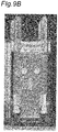
- the flow of the curable resin was observed after filling of the recess of the electromagnetic relay with the curable resin until curing of the curable resin in similar conditions to those in Working Example 3 except that a movable contact terminal having a shape with a closed clearance between the clearance forming portions was used (see Fig. 9B ).
- the seal structure according to the present invention is not restricted to the foregoing electromagnetic relay, but is also applicable to any electronic devices such as a switch and a sensor.
Landscapes
- Physics & Mathematics (AREA)
- Electromagnetism (AREA)
- Engineering & Computer Science (AREA)
- Manufacturing & Machinery (AREA)
- Switch Cases, Indication, And Locking (AREA)
Abstract
Description
- The present invention relates to an electronic-device seal structure and an electromagnetic relay using this electronic-device seal structure.
- Japanese Unexamined Patent Application Publication No.
2000-260283 case 44, and/or a cut-and-raised part is provided in a movable contact terminal. - PTL 1: Japanese Unexamined Patent Application Publication No.
2000-260283 - However, in the conventional seal structure, a component such as the case or the movable contact terminal is required to have high accuracy, thus causing problems where variations tend to occur in sealing properties inside the case and manufacturing cost is high.
- In view of the foregoing problems, an object of the present invention is to provide an electronic-device seal structure that facilitates manufacturing of an electronic device and enables reduction in manufacturing cost.
- In order to solve the above problems, an electronic-device seal structure according to one embodiment of the present invention comprises: a base; a case which covers an upper surface of the base and has an opening at a surface thereof; and a pair of terminals attached to the base, wherein a first clearance sealed with a sealing material is provided between the base and the case, characterized in that a second clearance is provided between the pair of the terminals disposed on an end surface of the base to face each other.
- With the electronic-device seal structure according to this embodiment of the present invention, the second clearance is provided between the pair of terminals disposed on the end surface of the base to face each other so that a space inside the case can be sealed by the sealing material, thereby eliminating the need for the component with high component accuracy. This facilitates manufacturing of the electronic device and enables reduction in manufacturing cost.
- In one embodiment of the present invention, the electronic-device seal structure further comprises clearance forming portions which form the second clearance and are provided on bases of the pair of terminals to face each other.
- According to this embodiment, an electronic device with high flexibility in design can be obtained.
- In one embodiment of the present invention, each of the pair of terminals is a laminate configured by folding and superimposing a plate-like member.
- According to this embodiment, an electronic device with high flexibility in design can be obtained.
- In one embodiment of the present invention, a dimension from a body of each of the pair of terminals to an inner surface of the case is not smaller than 0.16 mm and not larger than 0.25 mm, the second clearance between the clearance forming portions is not larger than 2.0 mm, a longitudinal dimension of a facing portion of each of the clearance forming portions is not larger than 2.1 mm, and the sealing material has a viscosity of 39000 to 48000 mPa·s in a range of 25±5°C.
- According to this embodiment, it is possible to reduce an inflow distance of the sealing material that flows from the second clearance between the clearance forming portions to the inside of the case by setting the second clearance to not larger than 2. 0 mm when the dimension from the body of the terminal to the inner surface of the case is set to not smaller than 0.16 mm and not larger than 0.25 mm, the longitudinal dimension of the facing portion of each of the clearance forming portions of the pair of terminals is set to not larger than 2.1 mm, and the sealing material with the viscosity of 39000 to 48000 mPa·s in the range of 25±5°C is used. This eliminates the need to prevent the inflow of the sealing material to the inside of the case by providing a configuration such as a projection or a cut-and-raised part in the movable contact terminal or by increasing a height dimension of the electronic device, so as to prevent the inflow of the sealing material to the inside of the case. As a result, the manufacturing cost of the electronic device can be reduced.
- When a sealing material with a viscosity smaller than 39000 mPa·s in the range of 25±5°C is used, the sealing material flows to the deep inside of the
case 30. When a sealing material with a viscosity larger than 48000 mPa·s in the range of 25±5°C is used, the sealing material cannot sufficiently fill the first clearance between the base and the case, and cannot ensure the sealing properties inside the case. Therefore, the use of the sealing material with the above temperature and viscosity facilitates control of the sealing material that flows to the inside of the case, while maintaining the sealing properties inside the case. - In one embodiment of the present invention, the second clearance between the pair of terminals is not larger than 0.5 mm.
- According to this embodiment, it is possible to reliably reduce the inflow distance of the sealing material from the second clearance between the clearance forming portions to the inside of the case, and thereby to reduce the manufacturing cost of the electronic device.
- In one embodiment of the present invention, the first clearance between the base and the case is not smaller than 0.01 mm and not larger than 0.10 mm
- According to this embodiment, when the first clearance between the base and the case is less than 0.01 mm, capillarity action might occur to cause the sealing material to flow to the inside of the case. Further, when the first clearance between the base and the case is more than 0.10 mm, it becomes difficult to control the inflow of the sealing material to the inside of the case. Thus, providing the first clearance with the above dimension facilitates control of the sealing material that flows to the inside of the case.
- In one embodiment of the present invention, the seal structure further comprises tapered portions provided at facing edges of the pair of terminals.
- According to this embodiment, it becomes easier to control the sealing material that flows to the inside of the case.
- In one embodiment of the present invention, an angle of each of the tapered portions is not smaller than 20°.
- According to this embodiment, it becomes easier to control the sealing material that flows to the inside of the case.
- An electromagnetic relay according to one embodiment of the present invention is characterized by having the electronic-device seal structure.
- According to this embodiment of the present invention, it is possible to obtain an electromagnetic relay that is manufactured with ease at low cost.
-
-
Fig. 1 is a perspective view showing an electromagnetic relay that is an electronic device according to one embodiment of the present invention. -
Fig. 2 is a perspective view showing a state in which a case of the electromagnetic relay inFig. 1 has been removed. -
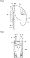
Fig. 3 is an enlarged transverse sectional view showing a movable contact terminal of the electromagnetic relay inFig. 1 . -
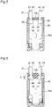
Fig. 4 is a longitudinal sectional view showing a state before sealing of the bottom surface of the electromagnetic relay inFig. 1 with epoxy resin. -
Fig. 5 is a longitudinal sectional view showing a state in the middle of the sealing of the bottom surface of the electromagnetic relay inFig. 1 with the epoxy resin, with a direction, from which the epoxy resin is poured, oriented upward. -
Fig. 6 is a longitudinal sectional view showing a state after the sealing of the bottom surface of the electromagnetic relay inFig. 1 with the epoxy resin, with the direction, from which the epoxy resin is poured, oriented upward. -
Figs. 7A and 7B show Working Example 1. -
Figs. 8A and8B show Working Example 2. -
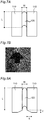
Figs. 9A and9B show Working Example 3. -
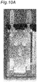
Figs. 10A and10B show Working Example 3 subsequent toFigs. 9A and9B . -
Fig. 11 shows Working Example 3 subsequent toFigs. 10A and10B . - Hereinafter, an electromagnetic relay according to one embodiment of the present invention will be described in accordance with the attached drawings.
- As shown in
Figs. 1 and 2 , an electromagnetic relay according to one embodiment of the present embodiment includes abase 10, an electromagnet unit 20 provided on thisbase 10, and acase 30 that covers thebase 10 and the electromagnet unit 20. The electromagnet unit 20 is assembled with a movable contact terminal 40, a normally-open fixedcontact terminal 50, and a normally-closed fixed contact part 60. Further, as shown inFigs. 5 and 6 , in the electromagnetic relay, an internal space in thecase 30 is sealed with a sealing material (sealant) 100. Note that the sealingmaterial 100 is shown only inFigs. 5 and 6 for convenience of the description. - As shown in
Fig. 2 , thebase 10 has notches 11 (only one ofnotches 11 is shown inFig. 2 ) at both ends in a width direction for protruding movableterminal parts terminal part 51 downward. Further, although not shown in the drawings, thebase 10 is provided with a terminal hole into whichcoil terminals 21 are pressed, and press holes for fixing the normally-open fixedcontact terminal 50 and the normally-closed fixed contact part 60, and the like. - As shown in
Fig. 2 , the electromagnet unit 20 has a spool 22 integrally molded into thebase 10, a coil 23 wound around a trunk of this spool 22, and a yoke 24 having an L-shaped cross section and assembled to the spool 22. A flange 22a is provided in an upper part of the spool 22. The yoke 24 is made up of avertical portion 24a extending along the coil 23, and a horizontal portion, not shown. The lower end of an iron core (not shown) inserted into the trunk of the spool 22 is swaged and fixed to the horizontal portion. - As shown in
Fig. 4 , thecase 30 has a boxed shape with an opening at one surface thereof, and has an external shape fittable to thebase 10. - As shown in
Fig. 2 , the movable contact terminal 40 is formed of a conductive plate spring with a substantially L shape, and has abody 40a, a pair of movableterminal parts body 40a, and amovable contact piece 42 at the other end of thebody 40a. Thismovable contact piece 42 is provided with amovable contact 43 at its free end and amovable iron piece 45 on its lower surface. The movable contact terminal 40 is swaged and fixed to thevertical portion 24a of the yoke 24. - The movable
terminal parts body 40a so as to face each other with a predetermined interval. In the bases of the movableterminal parts body 40a. A clearance 46 (second clearance) is defined by the clearance forming portions 41a, 41a on thebody 40a. Further, taperedportions - As shown in
Fig. 2 , the normally-open fixedcontact terminal 50 has ahorizontal portion 52 provided with a normally-openfixed contact 53 at its upper end, and has the fixedterminal part 51 at its lower end. Further, a pressing terminal part, not shown, is provided on a lower end of the normally-open fixedcontact terminal 50. By pressing this pressing terminal part into the press hole of thebase 10, the normally-open fixedcontact terminal 50 is fixed to thebase 10. - As shown in
Fig. 2 , the normally-closed fixed contact part 60 has a horizontal portion 62 provided with a normally-closedfixed contact 63 at its upper end. Further, a pressing terminal part, not shown, is provided at the lower end of the normally-closed fixed contact part 60. By pressing this pressing terminal part into the press hole of thebase 10, the normally-closed fixed contact part 60 is fixed to thebase 10. - Next, a procedure of assembling the electromagnetic relay will be described.
- First, the coil 23 is wound around the trunk of the spool 22 with the
coil terminals base 10. Then, lead wires of this coil 23 are bound and soldered to thecoil terminals - Next, an iron core is inserted into the trunk of the spool 22, and this iron core is swaged and fixed to the horizontal portion of the yoke 24 assembled to the
base 10, to be formed into one piece. - Subsequently, the movable contact terminal 40 is swaged and fixed to the
vertical portion 24a of the yoke 24, and the normally-open fixedcontact terminal 50 and the normally-closed fixed contact part 60 are fixed to thebase 10. At this time, themovable iron piece 45 is rotatably supported by the upper end of the yoke 24, and themovable contact 43 faces the normally-openfixed contact 53 and the normally-closedfixed contact 63 so as to alternately contact with/separate from the normally-openfixed contact 53 and alternately contact with/separate from the normally-closedfixed contact 63. - Finally, the
case 30 is fitted to thebase 10, and thereafter, curable resin is poured as the sealingmaterial 100 into arecess 70 formed of the bottom surface of thebase 10 and the opening edge of the case 30 (seeFig. 4 ). Then, the sealingmaterial 100 is cured to complete the assembly operation. - Here, the sealing
material 100 is preferably curable resin with a viscosity from 39000 to 48000 mPa·s, measured in the range of normal temperature (25±5°C) in conformity to JIS K-6833 Section 6.3. - This is because, when curable resin with a viscosity of less than 39000 mPa·s at normal temperature is used, the curable resin does not stay in the
recess 70, but flows to the deep inside of thecase 30. When curable resin with a viscosity of more than 48000 mPa·s at normal temperature is used, the curable resin cannot sufficiently fill a clearance (first clearance) between the base 10 and thecase 30, and cannot ensure the sealing properties inside thecase 30. - Note that examples of the curable resin include thermosetting resin, ultraviolet curable resin, and anaerobic curable resin.
- Further, when the foregoing curable resin is to be used as the sealing
material 100, at the time of fitting of thecase 30 to thebase 10, it is preferable to provide a clearance with a dimension H0 (shown inFig. 3 ) of not smaller than 0.01 mm and not larger than 0.10 mm between a side surface of thebase 10 and the inner surface of thecase 30 except for a part of the movable contact terminal 40, and it is more preferable to provide a clearance with a dimension H0 of 0.05 mm. - This is because, when the dimension H0 of the clearance between the side surface of the
base 10 and the inner surface of thecase 30 is smaller than 0.01 mm, capillarity action might occur to cause the curable resin to flow to the inside of thecase 30. When the dimension H0 of the clearance between the side surface of thebase 10 and the inner surface of thecase 30 is larger than 0.10 mm, it becomes difficult to control the inflow of the curable resin to the inside of thecase 30. - Note that the dimension H0 of the clearance is a dimension of the clearance between the inner surface of the
case 30 and the outer surface of the base 10 in the state of being fitted with the electromagnet unit 20, the movable contact terminal 40, the normally-open fixedcontact terminal 50, and the normally-closed fixed contact part 60. Hence, a dimensional tolerance of the clearance between the outer surface of thebase 10 and the inner surface of thecase 30 may be set within a range of not smaller than 0.01 mm and not larger than 0.10 mm. - Subsequently, the seal structure of the movable contact terminal 40 will be described using
Figs. 4 to 6 . - As shown in
Fig. 4 , the assembled electromagnetic relay is turned upside down, and the sealingmaterial 100 is poured into therecess 70. As shown inFig. 5 , therecess 70 is filled with the sealingmaterial 100. The sealingmaterial 100 thus filled flows down from the clearance between the base 10 and thecase 30 to the inside of thecase 30 as the time passes until the sealingmaterial 100 is cured. - In the movable contact terminal 40, the
clearance 46 is defined between the movableterminal parts clearance 46, a dimension H1 (shown inFig. 3 ) between thebody 40a of the movable contact terminal 40 and the inner surface of thecase 30 is larger than the dimension H0 by a thickness of the plate spring. Thus, as shown inFig. 6 , an inflow distance L of the sealingmaterial 100 that flows from theclearance 46 between the movableterminal parts case 30 becomes longer than an inflow distance of the sealingmaterial 100 that flows from the clearance between the base 10 and thecase 30 toward the inside of thecase 30. - When the foregoing curable resin is used as the sealing
material 100 and the movable contact terminal 40 is formed of the plate spring with a thickness of 0.15 mm such that a longitudinal dimension L (shown inFig. 6 ) of the facing portion of each of the clearance forming portions 41a is 2.1 mm (i.e., when H1 is in a range of not smaller than 0.16 mm and not larger than 0.25 mm), a dimension W (shown inFig. 4 ) of theclearance 46 is preferably not larger than 2.0 mm, and more preferably not larger than 0.5 mm. Setting the dimension W of the clearance 4 to not larger than 2.0 mm, preferably to not larger than 0. 5 mm, can reduce the inflow distance of the sealingmaterial 100 that flows from theclearance 46 to the inside of thecase 30. This eliminates the need to prevent the inflow of the sealingmaterial 100 to the inside of thecase 30 by providing a configuration such as a projection or a cut-and-raised part in the movable contact terminal 40, or by increasing a height dimension of the electromagnetic relay, in order to prevent the inflow of the sealingmaterial 100 to the inside of thecase 30. As a result, the manufacturing cost of the electromagnetic relay can be reduced. - On the other hand, when the dimension W of the
clearance 46 is larger than 2.0 mm, it becomes difficult to control the inflow of the curable resin to the inside of thecase 30. - Further, providing the
tapered portions material 100 to the inside of thecase 30. - Note that the angles (tapered angles) of the tapered
portions material 100 to the inside of thecase 30. - In the electromagnetic relay, the clearance forming portion 41a is provided in each of the movable
terminal parts - Note that forming the clearance forming portion so as to prevent formation of the
clearance 46 can reduce an amount of inflow of the sealingmaterial 100 to the inside of thecase 30. However, when such a movable contact terminal is to be manufactured, it is necessary to process the plate spring such that the plate spring can cover the clearance between the clearance forming portions on the body at the time of hemming bending, thus making a feed pitch of the plate spring large to cause deterioration in cutting layout efficiency. - In contrast, in the above electromagnetic relay, since the
clearance 46 is defined between the clearance forming portions 41a, 41a, it is possible to make small the width dimension of the plate spring for forming each of the movableterminal parts material 100 to the inside of thecase 30. Hence, it is possible to improve the cutting layout efficiency while reducing the feed pitch of the plate spring, and thereby to enhance the productivity of the electromagnetic relay. - As shown in
Fig. 7A , plate springs 110, 110 constituting the movable contact terminal 40 were disposed facing each other so as to form a clearance of W1 = 2.0 mm by a thickness gauge, the curable resin was poured into this clearance, and an inflow distance rL of the curable resin into the clearance was measured. -
- Measurement was performed at an ambient temperature of 25±5°C.
- As the curable resin, there was used epoxy resin with a viscosity of 39000 to 48000 mPa·s at an ambient temperature in the range of 25±5°C.
- As the
plate spring 110, a thin stainless steel plate was used. - After pouring of the curable resin, the curable resin was allowed to stand for one hour or longer, and an inflow distance rL1 was measured.
- As a result of the measurement, the inflow distance rL1 of the curable resin was 2.1 mm.
- An inflow distance rL0 of the curable resin was measured in similar conditions to those in Working Example 1-1 except that the clearance between the plate springs 110, 110 was set to W0 = 0.5 mm.
- As a result of the measurement, the inflow distance rL0 of the curable resin was 1.7 mm.
- From the results of Working Example 1-1 and Comparative Example 1, it was found that narrowing the clearance between the plate springs 110, 110 from W1 = 2.0 mm to W0 = 0.5 mm leads to a decrease in value of the inflow distance rL of the curable resin.
- An inflow distance rL2 of the curable resin was measured in similar conditions to those in Working Example 1-1 except that the clearance between the plate springs 110, 110 was set to W2 = 4.0 mm.
- As a result of the measurement, the inflow distance rL2 of the curable resin was 6.5 mm.
- From the results of Working Example 1-2 and Comparative Example 1, it was found that widening the clearance between the plate springs 110, 110 from W0 = 0.5 mm to W2 = 4.0 mm leads to an increase in value of the inflow distance rL of the curable resin.
- As shown in
Fig. 8A , the plate springs 110 were disposed facing each other so as to form a clearance of W = 2.0 mm by the thickness gauge, the curable resin was poured into this clearance, and an inflow distance rL of the curable resin into the clearance was measured. At the lower end edge of theplate spring 110 of this working example, a tapered portion (a tapered angle of about 20°) formed with dimensions of X = 0.88 mm and Y = 0.3 mm was provided. -
- Measurement was performed at an ambient temperature of 25±5°C.
- As the curable resin, there was used epoxy resin with a viscosity of 39000 to 48000 mPa·s at an ambient temperature in the range of 25±5°C.
- As the
plate spring 110, a thin stainless steel plate was used. - After pouring of the curable resin, the curable resin was allowed to stand for one hour or longer, and an inflow distance rL1 was measured.
- As a result of the measurement, the inflow distance rL1 of the curable resin was 1.8 mm.
- An inflow distance rL0 of the curable resin was measured in similar conditions to those in Working Example 2-1 except that no tapered portion was provided.
- As a result of the measurement, the inflow distance rL0 of the curable resin was 1.9 mm.
- From the results of Working Example 2-1 and Comparative Example 2, it was found that providing the tapered portions leads to a decrease in value of the inflow distance rL of the curable resin.
- An inflow distance rL2 of the curable resin was measured in similar conditions to those in Working Example 2-1 except that the tapered portion was formed with dimensions of X = 0.35 mm and Y = 0.3 mm (a tapered angle of about 60°).
- As a result of the measurement, the inflow distance rL2 of the curable resin was 1.7 mm.
- From the results of Working Example 2-2 and Comparative Example 2, it was found that increasing the angle of the tapered portion leads to a decrease in value of the inflow distance rL of the curable resin.
- The flow of the curable resin was observed after filling of the recess of the electromagnetic relay shown in
Fig. 1 with the curable resin until curing of the curable resin. -
- The electromagnetic relay with the configuration shown in
Fig. 1 was used. In this electromagnetic relay, a plate spring with a thickness of 0.15 mm was used for the movable contact terminal not provided with the tapered portion, and the thickness of the movable terminal part was set to 0.30 mm. Further, a clearance of W =2.0 mm (a dimension, H1= 0.20 mm, of the clearance between the base and the body) was provided between the clearance forming portions on the bodies of the movable contact terminals. For observing the inflow of the curable resin into the clearance between the clearance forming portions, a transparent case was used (seeFig. 9A ). - As the plate spring, a thin stainless steel plate was used.
- A dimensional tolerance of the clearance between the outer surface of the base and the inner surface of the case was set to a range of not smaller than 0.01 mm and not larger than 0.10 mm.
- The measurement was performed at an ambient temperature of 23°C.
- As the curable resin, there was used epoxy resin with a viscosity of 39000 to 48000 mPa·s at an ambient temperature in the range of 25±5°C.
-
- After filling of the recess of the electromagnetic relay with the curable resin, the curable resin was allowed to stand. The curable resin that flows into the clearance between the movable terminal parts was then photographed every one minute until 30 minutes elapsed from the filling with the curable resin.
- Next, the electromagnetic relay was put into a thermostatic oven at 50°C, and the curable resin that flows into the clearance between the clearance forming portions was photographed every five minutes until 250 minutes elapsed from the filling with the curable resin. The electromagnetic relay was taken out from the thermostatic oven every five minutes, for performing the photographing.
- As a result of the observation, at normal temperature, the inflow of the curable resin was stopped in about 15 minutes, and became immobilized (see
Fig. 10A ). Further, after the putting into the thermostatic oven, the inflow of the curable resin was stopped in about 60 minutes, and became immobilized (see the views (A) and (B) ofFig. 11 ). It was thereby found that, even after the lapse of the time, the curable resin does not flow to the inside of the case from the clearance between the clearance forming portions on the bodies. - The flow of the curable resin was observed after filling of the recess of the electromagnetic relay with the curable resin until curing of the curable resin in similar conditions to those in Working Example 3 except that a movable contact terminal having a shape with a closed clearance between the clearance forming portions was used (see
Fig. 9B ). - As a result of the observation, at normal temperature, the inflow of the curable resin was stopped in about 15 minutes, and became immobilized (see
Fig. 10B ). Further, after the putting into the thermostatic oven, the inflow of the curable resin was stopped in about 60 minutes, and became immobilized (seeFig. 11 ). It was thereby found that, even after the lapse of the time, the curable resin does not flow from between the movable terminal parts to the inside of the case. - From the results of Working Example 3 and Comparative Example 3, it was found that the inflow of the curable resin to the inside of the case can be reduced even without completely closing the clearance between the movable terminal parts.
- It was found from Working Example 1 and Working Example 3 above that, when the epoxy resin with a viscosity of 39000 to 48000 mPa·s at an ambient temperature in the range of 25±5°C was used as the curable resin and the movable contact terminal was formed of a plate spring with a thickness of 0.15 mm such that the height dimension L of the clearance forming portion 41a was 2.1 mm (the dimension H1 of the clearance between the base and the body of the clearance forming portion was in the range of not smaller than 0.16 mm and not larger than 0.26 mm), it is possible to reduce the inflow distance rL of the curable resin that flows from the clearance between the clearance forming portions to the inside of the case to not longer than 2.1 mm by setting the dimension of the clearance to W = 2.0 mm. Further, it was found from Working Example 2 that providing the tapered portion at each of the facing edges of the movable contact part and increasing the tapered angle of this tapered portion can lead to reduction in the inflow distance rL of the curable resin that flows from the clearance between the clearance forming portions to the inside of the case.
- The seal structure according to the present invention is not restricted to the foregoing electromagnetic relay, but is also applicable to any electronic devices such as a switch and a sensor.
-
- 10. base
- 11. notch
- 20. electromagnet unit
- 21. coil terminal
- 22. spool
- 22a. flange
- 23. coil
- 24. yoke
- 24a. vertical portion
- 30. case
- 40. movable contact terminal
- 40a. body
- 41. movable terminal part
- 41a. clearance forming portion
- 42. movable contact piece
- 43. movable contact
- 44. tapered portion
- 45. movable iron piece
- 46. clearance
- 50. normally-open fixed contact terminal
- 51. fixed terminal
- 52. horizontal portion
- 53. normally-open fixed contact
- 60. normally-closed fixed contact part
- 62. horizontal portion
- 63. normally-closed fixed contact
- 70. recess
- 100. sealing material
- 110. thickness gauge
Claims (9)
- An electronic-device seal structure comprising:a base;a case which covers an upper surface of the base and has an opening at a surface thereof; anda pair of terminals attached to the base, whereina first clearance sealed with a sealing material is provided between the base and the case, characterized in thata second clearance is provided between the pair of the terminals disposed on an end surface of the base to face each other.
- The seal structure as claimed in claim 1, characterized in that
the seal structure further comprises clearance forming portions which form the second clearance and are provided on bases of the pair of terminals to face each other. - The seal structure as claimed in claim 2, characterized in that
each of the pair of terminals is a laminate configured by folding and superimposing a plate-like member. - The seal structure as claimed in claim 2 or 3, characterized in that
a dimension from a body of each of the pair of terminals to an inner surface of the case is not smaller than 0.16 mm and not larger than 0.25 mm, the second clearance between the clearance forming portions is not larger than 2.0 mm, a longitudinal dimension of a facing portion of each of the clearance forming portions is not larger than 2.1 mm, and the sealing material has a viscosity of 39000 to 48000 mPa·s in a range of 25±5°C. - The seal structure as claimed in claim 4, characterized in that
the second clearance between the pair of terminals is not larger than 0.5 mm. - The seal structure as claimed in any one of claims 1 to 5, characterized in that
the first clearance between the base and the case is not smaller than 0.01 mm and not larger than 0.10 mm. - The seal structure as claimed in any one of claims 1 to 6, characterized in that
the seal structure further comprises tapered portions provided at facing edges of the pair of terminals. - The seal structure as claimed in claim 7, characterized in that
an angle of each of the tapered portions is not smaller than 20°. - An electromagnetic relay comprising an electronic-device seal structure claimed in any one of claims 1 to 8.
Applications Claiming Priority (2)
| Application Number | Priority Date | Filing Date | Title |
|---|---|---|---|
| JP2014052209A JP6291931B2 (en) | 2014-03-14 | 2014-03-14 | Electronic device seal structure and electromagnetic relay using the electronic device seal structure |
| PCT/JP2014/080975 WO2015136786A1 (en) | 2014-03-14 | 2014-11-21 | Electronic-device seal structure and electromagnetic relay using said electronic-device seal structure |
Publications (3)
| Publication Number | Publication Date |
|---|---|
| EP3118879A1 true EP3118879A1 (en) | 2017-01-18 |
| EP3118879A4 EP3118879A4 (en) | 2017-11-08 |
| EP3118879B1 EP3118879B1 (en) | 2019-06-12 |
Family
ID=54071251
Family Applications (1)
| Application Number | Title | Priority Date | Filing Date |
|---|---|---|---|
| EP14885349.2A Active EP3118879B1 (en) | 2014-03-14 | 2014-11-21 | Electronic-device seal structure and electromagnetic relay using said electronic-device seal structure |
Country Status (6)
| Country | Link |
|---|---|
| US (1) | US10153114B2 (en) |
| EP (1) | EP3118879B1 (en) |
| JP (1) | JP6291931B2 (en) |
| KR (1) | KR20160117564A (en) |
| CN (1) | CN106030749B (en) |
| WO (1) | WO2015136786A1 (en) |
Cited By (2)
| Publication number | Priority date | Publication date | Assignee | Title |
|---|---|---|---|---|
| EP3629355A1 (en) * | 2018-09-27 | 2020-04-01 | Panasonic Intellectual Property Management Co., Ltd. | Electric apparatus and electromagnetic relay |
| DE112017007138B4 (en) | 2017-02-28 | 2024-08-14 | Omron Corporation | Sealing structure of an electronic device, electronic device provided with sealing structure and manufacturing method of the electronic device |
Families Citing this family (9)
| Publication number | Priority date | Publication date | Assignee | Title |
|---|---|---|---|---|
| JP6291931B2 (en) * | 2014-03-14 | 2018-03-14 | オムロン株式会社 | Electronic device seal structure and electromagnetic relay using the electronic device seal structure |
| JP2016110843A (en) * | 2014-12-05 | 2016-06-20 | オムロン株式会社 | Electromagnetic relay |
| JP6414453B2 (en) * | 2014-12-05 | 2018-10-31 | オムロン株式会社 | Electromagnetic relay |
| JP6365684B2 (en) * | 2014-12-05 | 2018-08-01 | オムロン株式会社 | Electromagnetic relay |
| JP6631068B2 (en) * | 2015-07-27 | 2020-01-15 | オムロン株式会社 | Contact mechanism and electromagnetic relay using the same |
| JP6972710B2 (en) * | 2017-06-30 | 2021-11-24 | オムロン株式会社 | relay |
| JP7204365B2 (en) | 2018-07-31 | 2023-01-16 | 富士通コンポーネント株式会社 | electromagnetic relay |
| JP7154151B2 (en) * | 2019-02-15 | 2022-10-17 | 富士通コンポーネント株式会社 | Electromagnetic relay terminals and electromagnetic relays |
| IT202100018770A1 (en) * | 2021-07-15 | 2023-01-15 | Miotti S R L | TEMPERATURE LIMITER DEVICE |
Family Cites Families (29)
| Publication number | Priority date | Publication date | Assignee | Title |
|---|---|---|---|---|
| US3351876A (en) * | 1964-10-26 | 1967-11-07 | Hughes Aircraft Co | Electrical transmission system |
| DE2622133A1 (en) | 1976-05-18 | 1977-12-08 | Siemens Ag | ELECTRICAL COMPONENT, IN PARTICULAR ELECTROMAGNETIC RELAY |
| JPS5911817B2 (en) | 1981-09-21 | 1984-03-17 | 工業技術院長 | Temperature control method for solar heat collector |
| JPS5849855U (en) * | 1981-09-30 | 1983-04-04 | オムロン株式会社 | sealed relay |
| JPS6162191U (en) * | 1984-09-28 | 1986-04-26 | ||
| JPS61178244A (en) | 1985-02-04 | 1986-08-09 | Nissan Motor Co Ltd | Alarming device for vehicle |
| JPS61178244U (en) * | 1985-04-24 | 1986-11-07 | ||
| JPH056254A (en) | 1991-02-13 | 1993-01-14 | Oki Electric Ind Co Ltd | Display position control system for window |
| JPH056254U (en) * | 1991-07-05 | 1993-01-29 | 愛知機械工業株式会社 | Cover mounting structure for continuously variable transmission |
| JP3548749B2 (en) * | 1993-09-17 | 2004-07-28 | オムロン株式会社 | Electromagnetic relay |
| EP0720194B1 (en) * | 1993-09-17 | 2000-12-06 | Omron Corporation | Electromagnetic relay |
| JP3593774B2 (en) * | 1996-01-09 | 2004-11-24 | オムロン株式会社 | Electromagnetic relay |
| DE69931586T2 (en) * | 1998-12-07 | 2007-05-31 | Matsushita Electric Works, Ltd., Kadoma | Electromagnetic relay |
| JP3714006B2 (en) * | 1999-03-05 | 2005-11-09 | オムロン株式会社 | Electromagnetic relay |
| JP2000315448A (en) * | 1999-05-06 | 2000-11-14 | Omron Corp | Electromagnetic relay |
| JP2002100274A (en) * | 2000-09-26 | 2002-04-05 | Omron Corp | Electromagnetic relay |
| DE10209810B4 (en) * | 2001-03-09 | 2006-11-16 | Omron Corporation | relay |
| JP3870049B2 (en) * | 2001-08-17 | 2007-01-17 | Necトーキン株式会社 | Electromagnetic relay device |
| JP3898021B2 (en) * | 2001-10-05 | 2007-03-28 | 株式会社タイコーデバイス | Electromagnetic relay |
| JP4168733B2 (en) * | 2002-11-12 | 2008-10-22 | オムロン株式会社 | Electromagnetic relay |
| JP4190379B2 (en) * | 2003-09-12 | 2008-12-03 | 富士通コンポーネント株式会社 | Combined electromagnetic relay |
| US6949997B2 (en) * | 2003-09-26 | 2005-09-27 | Rockwell Automation Technologies, Inc. | Bi-stable trip-free relay configuration |
| JP4389653B2 (en) * | 2004-04-30 | 2009-12-24 | オムロン株式会社 | Electromagnetic relay |
| US20070084633A1 (en) | 2005-09-21 | 2007-04-19 | Tyco Electronic Corporation | Electromagnetic relay with noise reducing sealant |
| JP5494042B2 (en) * | 2010-03-12 | 2014-05-14 | オムロン株式会社 | Contact switching structure and electromagnetic relay |
| JP2011191885A (en) * | 2010-03-12 | 2011-09-29 | Omron Corp | Input device and pointing device |
| JP5741338B2 (en) | 2011-09-15 | 2015-07-01 | オムロン株式会社 | Terminal member seal structure and electromagnetic relay |
| JP6065661B2 (en) * | 2013-03-08 | 2017-01-25 | オムロン株式会社 | Electromagnetic relay |
| JP6291931B2 (en) * | 2014-03-14 | 2018-03-14 | オムロン株式会社 | Electronic device seal structure and electromagnetic relay using the electronic device seal structure |
-
2014
- 2014-03-14 JP JP2014052209A patent/JP6291931B2/en active Active
- 2014-11-21 KR KR1020167024255A patent/KR20160117564A/en not_active Withdrawn
- 2014-11-21 CN CN201480076175.9A patent/CN106030749B/en active Active
- 2014-11-21 EP EP14885349.2A patent/EP3118879B1/en active Active
- 2014-11-21 US US15/125,195 patent/US10153114B2/en active Active
- 2014-11-21 WO PCT/JP2014/080975 patent/WO2015136786A1/en not_active Ceased
Cited By (2)
| Publication number | Priority date | Publication date | Assignee | Title |
|---|---|---|---|---|
| DE112017007138B4 (en) | 2017-02-28 | 2024-08-14 | Omron Corporation | Sealing structure of an electronic device, electronic device provided with sealing structure and manufacturing method of the electronic device |
| EP3629355A1 (en) * | 2018-09-27 | 2020-04-01 | Panasonic Intellectual Property Management Co., Ltd. | Electric apparatus and electromagnetic relay |
Also Published As
| Publication number | Publication date |
|---|---|
| CN106030749B (en) | 2019-03-08 |
| US10153114B2 (en) | 2018-12-11 |
| CN106030749A (en) | 2016-10-12 |
| JP6291931B2 (en) | 2018-03-14 |
| JP2015176754A (en) | 2015-10-05 |
| US20170076893A1 (en) | 2017-03-16 |
| KR20160117564A (en) | 2016-10-10 |
| EP3118879A4 (en) | 2017-11-08 |
| WO2015136786A1 (en) | 2015-09-17 |
| EP3118879B1 (en) | 2019-06-12 |
Similar Documents
| Publication | Publication Date | Title |
|---|---|---|
| EP3118879B1 (en) | Electronic-device seal structure and electromagnetic relay using said electronic-device seal structure | |
| US9083100B2 (en) | Connection terminal and method for manufacturing connection terminal | |
| CN105284007B (en) | The end structure of covered electric cable | |
| CN103295718B (en) | The electromagnetically operated valve of mold pressing coil and use mold pressing coil and the manufacture method of mold pressing coil | |
| WO2013187529A1 (en) | Method of resin molding, metal mold for resin molding, and terminal fitting | |
| JP5910682B2 (en) | Electrical connector | |
| US20140106625A1 (en) | Connector and manufacturing method of connector | |
| CN107003201A (en) | Semiconductor pressure sensor device | |
| CN103975486A (en) | Connection terminal and connection terminal manufacturing method | |
| US10608370B2 (en) | Wire with a core, a terminal with barrels crimped to the core and a molded portion covering the barrels and the core | |
| JP2018014313A (en) | Electric wire with terminal | |
| CN112566400A (en) | Shell body | |
| JP5257677B2 (en) | Resin encapsulated electrical parts | |
| WO2017065041A1 (en) | Connector and wire with terminal | |
| US10411366B2 (en) | Connector housing containing a wire terminal with a molded portion | |
| WO2015019847A1 (en) | Connector | |
| JP6106653B2 (en) | Waterproof connector | |
| KR101684819B1 (en) | Method for manufacturing terminal, and terminal | |
| JP2012043642A (en) | Electromagnetic relay | |
| US20150114146A1 (en) | Sensor | |
| JP2015008309A (en) | Molded coil and solenoid valve using molded coil | |
| JP2008306819A (en) | Conductive material | |
| JP6739029B2 (en) | Seat plate for electronic parts | |
| JP6003817B2 (en) | Method for manufacturing terminal of liquid level detection device | |
| CN105449602A (en) | Liquid substance component analyzing device |
Legal Events
| Date | Code | Title | Description |
|---|---|---|---|
| PUAI | Public reference made under article 153(3) epc to a published international application that has entered the european phase |
Free format text: ORIGINAL CODE: 0009012 |
|
| STAA | Information on the status of an ep patent application or granted ep patent |
Free format text: STATUS: REQUEST FOR EXAMINATION WAS MADE |
|
| 17P | Request for examination filed |
Effective date: 20161004 |
|
| AK | Designated contracting states |
Kind code of ref document: A1 Designated state(s): AL AT BE BG CH CY CZ DE DK EE ES FI FR GB GR HR HU IE IS IT LI LT LU LV MC MK MT NL NO PL PT RO RS SE SI SK SM TR |
|
| AX | Request for extension of the european patent |
Extension state: BA ME |
|
| DAX | Request for extension of the european patent (deleted) | ||
| A4 | Supplementary search report drawn up and despatched |
Effective date: 20171011 |
|
| RIC1 | Information provided on ipc code assigned before grant |
Ipc: H01H 49/00 20060101ALI20171005BHEP Ipc: H01H 50/00 20060101ALI20171005BHEP Ipc: H01H 50/02 20060101AFI20171005BHEP Ipc: H01H 50/04 20060101ALI20171005BHEP |
|
| GRAP | Despatch of communication of intention to grant a patent |
Free format text: ORIGINAL CODE: EPIDOSNIGR1 |
|
| STAA | Information on the status of an ep patent application or granted ep patent |
Free format text: STATUS: GRANT OF PATENT IS INTENDED |
|
| RIN1 | Information on inventor provided before grant (corrected) |
Inventor name: TSUJI, KEISUKE Inventor name: MIYAKE, AYAKA Inventor name: KINOSHITA, MASAHIRO Inventor name: SASAKI, JUN Inventor name: TSUTSUI, KAZUHIRO |
|
| INTG | Intention to grant announced |
Effective date: 20190109 |
|
| GRAS | Grant fee paid |
Free format text: ORIGINAL CODE: EPIDOSNIGR3 |
|
| GRAA | (expected) grant |
Free format text: ORIGINAL CODE: 0009210 |
|
| STAA | Information on the status of an ep patent application or granted ep patent |
Free format text: STATUS: THE PATENT HAS BEEN GRANTED |
|
| AK | Designated contracting states |
Kind code of ref document: B1 Designated state(s): AL AT BE BG CH CY CZ DE DK EE ES FI FR GB GR HR HU IE IS IT LI LT LU LV MC MK MT NL NO PL PT RO RS SE SI SK SM TR |
|
| REG | Reference to a national code |
Ref country code: GB Ref legal event code: FG4D |
|
| REG | Reference to a national code |
Ref country code: CH Ref legal event code: EP |
|
| REG | Reference to a national code |
Ref country code: AT Ref legal event code: REF Ref document number: 1143663 Country of ref document: AT Kind code of ref document: T Effective date: 20190615 |
|
| REG | Reference to a national code |
Ref country code: DE Ref legal event code: R096 Ref document number: 602014048442 Country of ref document: DE |
|
| REG | Reference to a national code |
Ref country code: IE Ref legal event code: FG4D |
|
| REG | Reference to a national code |
Ref country code: NL Ref legal event code: MP Effective date: 20190612 |
|
| REG | Reference to a national code |
Ref country code: LT Ref legal event code: MG4D |
|
| PG25 | Lapsed in a contracting state [announced via postgrant information from national office to epo] |
Ref country code: NO Free format text: LAPSE BECAUSE OF FAILURE TO SUBMIT A TRANSLATION OF THE DESCRIPTION OR TO PAY THE FEE WITHIN THE PRESCRIBED TIME-LIMIT Effective date: 20190912 Ref country code: FI Free format text: LAPSE BECAUSE OF FAILURE TO SUBMIT A TRANSLATION OF THE DESCRIPTION OR TO PAY THE FEE WITHIN THE PRESCRIBED TIME-LIMIT Effective date: 20190612 Ref country code: HR Free format text: LAPSE BECAUSE OF FAILURE TO SUBMIT A TRANSLATION OF THE DESCRIPTION OR TO PAY THE FEE WITHIN THE PRESCRIBED TIME-LIMIT Effective date: 20190612 Ref country code: LT Free format text: LAPSE BECAUSE OF FAILURE TO SUBMIT A TRANSLATION OF THE DESCRIPTION OR TO PAY THE FEE WITHIN THE PRESCRIBED TIME-LIMIT Effective date: 20190612 Ref country code: AL Free format text: LAPSE BECAUSE OF FAILURE TO SUBMIT A TRANSLATION OF THE DESCRIPTION OR TO PAY THE FEE WITHIN THE PRESCRIBED TIME-LIMIT Effective date: 20190612 Ref country code: SE Free format text: LAPSE BECAUSE OF FAILURE TO SUBMIT A TRANSLATION OF THE DESCRIPTION OR TO PAY THE FEE WITHIN THE PRESCRIBED TIME-LIMIT Effective date: 20190612 |
|
| PG25 | Lapsed in a contracting state [announced via postgrant information from national office to epo] |
Ref country code: BG Free format text: LAPSE BECAUSE OF FAILURE TO SUBMIT A TRANSLATION OF THE DESCRIPTION OR TO PAY THE FEE WITHIN THE PRESCRIBED TIME-LIMIT Effective date: 20190912 Ref country code: GR Free format text: LAPSE BECAUSE OF FAILURE TO SUBMIT A TRANSLATION OF THE DESCRIPTION OR TO PAY THE FEE WITHIN THE PRESCRIBED TIME-LIMIT Effective date: 20190913 Ref country code: LV Free format text: LAPSE BECAUSE OF FAILURE TO SUBMIT A TRANSLATION OF THE DESCRIPTION OR TO PAY THE FEE WITHIN THE PRESCRIBED TIME-LIMIT Effective date: 20190612 Ref country code: RS Free format text: LAPSE BECAUSE OF FAILURE TO SUBMIT A TRANSLATION OF THE DESCRIPTION OR TO PAY THE FEE WITHIN THE PRESCRIBED TIME-LIMIT Effective date: 20190612 |
|
| REG | Reference to a national code |
Ref country code: AT Ref legal event code: MK05 Ref document number: 1143663 Country of ref document: AT Kind code of ref document: T Effective date: 20190612 |
|
| PG25 | Lapsed in a contracting state [announced via postgrant information from national office to epo] |
Ref country code: SK Free format text: LAPSE BECAUSE OF FAILURE TO SUBMIT A TRANSLATION OF THE DESCRIPTION OR TO PAY THE FEE WITHIN THE PRESCRIBED TIME-LIMIT Effective date: 20190612 Ref country code: RO Free format text: LAPSE BECAUSE OF FAILURE TO SUBMIT A TRANSLATION OF THE DESCRIPTION OR TO PAY THE FEE WITHIN THE PRESCRIBED TIME-LIMIT Effective date: 20190612 Ref country code: CZ Free format text: LAPSE BECAUSE OF FAILURE TO SUBMIT A TRANSLATION OF THE DESCRIPTION OR TO PAY THE FEE WITHIN THE PRESCRIBED TIME-LIMIT Effective date: 20190612 Ref country code: PT Free format text: LAPSE BECAUSE OF FAILURE TO SUBMIT A TRANSLATION OF THE DESCRIPTION OR TO PAY THE FEE WITHIN THE PRESCRIBED TIME-LIMIT Effective date: 20191014 Ref country code: NL Free format text: LAPSE BECAUSE OF FAILURE TO SUBMIT A TRANSLATION OF THE DESCRIPTION OR TO PAY THE FEE WITHIN THE PRESCRIBED TIME-LIMIT Effective date: 20190612 Ref country code: EE Free format text: LAPSE BECAUSE OF FAILURE TO SUBMIT A TRANSLATION OF THE DESCRIPTION OR TO PAY THE FEE WITHIN THE PRESCRIBED TIME-LIMIT Effective date: 20190612 Ref country code: AT Free format text: LAPSE BECAUSE OF FAILURE TO SUBMIT A TRANSLATION OF THE DESCRIPTION OR TO PAY THE FEE WITHIN THE PRESCRIBED TIME-LIMIT Effective date: 20190612 |
|
| PG25 | Lapsed in a contracting state [announced via postgrant information from national office to epo] |
Ref country code: ES Free format text: LAPSE BECAUSE OF FAILURE TO SUBMIT A TRANSLATION OF THE DESCRIPTION OR TO PAY THE FEE WITHIN THE PRESCRIBED TIME-LIMIT Effective date: 20190612 Ref country code: IS Free format text: LAPSE BECAUSE OF FAILURE TO SUBMIT A TRANSLATION OF THE DESCRIPTION OR TO PAY THE FEE WITHIN THE PRESCRIBED TIME-LIMIT Effective date: 20191012 Ref country code: SM Free format text: LAPSE BECAUSE OF FAILURE TO SUBMIT A TRANSLATION OF THE DESCRIPTION OR TO PAY THE FEE WITHIN THE PRESCRIBED TIME-LIMIT Effective date: 20190612 Ref country code: IT Free format text: LAPSE BECAUSE OF FAILURE TO SUBMIT A TRANSLATION OF THE DESCRIPTION OR TO PAY THE FEE WITHIN THE PRESCRIBED TIME-LIMIT Effective date: 20190612 |
|
| REG | Reference to a national code |
Ref country code: DE Ref legal event code: R097 Ref document number: 602014048442 Country of ref document: DE |
|
| PG25 | Lapsed in a contracting state [announced via postgrant information from national office to epo] |
Ref country code: TR Free format text: LAPSE BECAUSE OF FAILURE TO SUBMIT A TRANSLATION OF THE DESCRIPTION OR TO PAY THE FEE WITHIN THE PRESCRIBED TIME-LIMIT Effective date: 20190612 |
|
| PLBE | No opposition filed within time limit |
Free format text: ORIGINAL CODE: 0009261 |
|
| STAA | Information on the status of an ep patent application or granted ep patent |
Free format text: STATUS: NO OPPOSITION FILED WITHIN TIME LIMIT |
|
| PG25 | Lapsed in a contracting state [announced via postgrant information from national office to epo] |
Ref country code: PL Free format text: LAPSE BECAUSE OF FAILURE TO SUBMIT A TRANSLATION OF THE DESCRIPTION OR TO PAY THE FEE WITHIN THE PRESCRIBED TIME-LIMIT Effective date: 20190612 Ref country code: DK Free format text: LAPSE BECAUSE OF FAILURE TO SUBMIT A TRANSLATION OF THE DESCRIPTION OR TO PAY THE FEE WITHIN THE PRESCRIBED TIME-LIMIT Effective date: 20190612 |
|
| 26N | No opposition filed |
Effective date: 20200313 |
|
| PG25 | Lapsed in a contracting state [announced via postgrant information from national office to epo] |
Ref country code: IS Free format text: LAPSE BECAUSE OF FAILURE TO SUBMIT A TRANSLATION OF THE DESCRIPTION OR TO PAY THE FEE WITHIN THE PRESCRIBED TIME-LIMIT Effective date: 20200224 Ref country code: SI Free format text: LAPSE BECAUSE OF FAILURE TO SUBMIT A TRANSLATION OF THE DESCRIPTION OR TO PAY THE FEE WITHIN THE PRESCRIBED TIME-LIMIT Effective date: 20190612 |
|
| REG | Reference to a national code |
Ref country code: CH Ref legal event code: PL |
|
| PG2D | Information on lapse in contracting state deleted |
Ref country code: IS |
|
| PG25 | Lapsed in a contracting state [announced via postgrant information from national office to epo] |
Ref country code: MC Free format text: LAPSE BECAUSE OF FAILURE TO SUBMIT A TRANSLATION OF THE DESCRIPTION OR TO PAY THE FEE WITHIN THE PRESCRIBED TIME-LIMIT Effective date: 20190612 Ref country code: LI Free format text: LAPSE BECAUSE OF NON-PAYMENT OF DUE FEES Effective date: 20191130 Ref country code: LU Free format text: LAPSE BECAUSE OF NON-PAYMENT OF DUE FEES Effective date: 20191121 Ref country code: CH Free format text: LAPSE BECAUSE OF NON-PAYMENT OF DUE FEES Effective date: 20191130 |
|
| REG | Reference to a national code |
Ref country code: BE Ref legal event code: MM Effective date: 20191130 |
|
| GBPC | Gb: european patent ceased through non-payment of renewal fee |
Effective date: 20191121 |
|
| PG25 | Lapsed in a contracting state [announced via postgrant information from national office to epo] |
Ref country code: IE Free format text: LAPSE BECAUSE OF NON-PAYMENT OF DUE FEES Effective date: 20191121 Ref country code: FR Free format text: LAPSE BECAUSE OF NON-PAYMENT OF DUE FEES Effective date: 20191130 Ref country code: GB Free format text: LAPSE BECAUSE OF NON-PAYMENT OF DUE FEES Effective date: 20191121 |
|
| PG25 | Lapsed in a contracting state [announced via postgrant information from national office to epo] |
Ref country code: BE Free format text: LAPSE BECAUSE OF NON-PAYMENT OF DUE FEES Effective date: 20191130 |
|
| PG25 | Lapsed in a contracting state [announced via postgrant information from national office to epo] |
Ref country code: CY Free format text: LAPSE BECAUSE OF FAILURE TO SUBMIT A TRANSLATION OF THE DESCRIPTION OR TO PAY THE FEE WITHIN THE PRESCRIBED TIME-LIMIT Effective date: 20190612 |
|
| PG25 | Lapsed in a contracting state [announced via postgrant information from national office to epo] |
Ref country code: HU Free format text: LAPSE BECAUSE OF FAILURE TO SUBMIT A TRANSLATION OF THE DESCRIPTION OR TO PAY THE FEE WITHIN THE PRESCRIBED TIME-LIMIT; INVALID AB INITIO Effective date: 20141121 Ref country code: MT Free format text: LAPSE BECAUSE OF FAILURE TO SUBMIT A TRANSLATION OF THE DESCRIPTION OR TO PAY THE FEE WITHIN THE PRESCRIBED TIME-LIMIT Effective date: 20190612 |
|
| PG25 | Lapsed in a contracting state [announced via postgrant information from national office to epo] |
Ref country code: MK Free format text: LAPSE BECAUSE OF FAILURE TO SUBMIT A TRANSLATION OF THE DESCRIPTION OR TO PAY THE FEE WITHIN THE PRESCRIBED TIME-LIMIT Effective date: 20190612 |
|
| PGFP | Annual fee paid to national office [announced via postgrant information from national office to epo] |
Ref country code: DE Payment date: 20251118 Year of fee payment: 12 |