EP3117227B1 - A method and apparatus for reconfiguring pin assignments on a connector - Google Patents
A method and apparatus for reconfiguring pin assignments on a connector Download PDFInfo
- Publication number
- EP3117227B1 EP3117227B1 EP14885760.0A EP14885760A EP3117227B1 EP 3117227 B1 EP3117227 B1 EP 3117227B1 EP 14885760 A EP14885760 A EP 14885760A EP 3117227 B1 EP3117227 B1 EP 3117227B1
- Authority
- EP
- European Patent Office
- Prior art keywords
- accessory
- connector
- type
- present
- pin assignment
- Prior art date
- Legal status (The legal status is an assumption and is not a legal conclusion. Google has not performed a legal analysis and makes no representation as to the accuracy of the status listed.)
- Active
Links
Images



Classifications
-
- G—PHYSICS
- G06—COMPUTING OR CALCULATING; COUNTING
- G06F—ELECTRIC DIGITAL DATA PROCESSING
- G06F13/00—Interconnection of, or transfer of information or other signals between, memories, input/output devices or central processing units
- G06F13/38—Information transfer, e.g. on bus
- G06F13/40—Bus structure
- G06F13/4063—Device-to-bus coupling
- G06F13/4068—Electrical coupling
-
- G—PHYSICS
- G06—COMPUTING OR CALCULATING; COUNTING
- G06F—ELECTRIC DIGITAL DATA PROCESSING
- G06F13/00—Interconnection of, or transfer of information or other signals between, memories, input/output devices or central processing units
- G06F13/38—Information transfer, e.g. on bus
- G06F13/382—Information transfer, e.g. on bus using universal interface adapter
- G06F13/385—Information transfer, e.g. on bus using universal interface adapter for adaptation of a particular data processing system to different peripheral devices
-
- H—ELECTRICITY
- H01—ELECTRIC ELEMENTS
- H01R—ELECTRICALLY-CONDUCTIVE CONNECTIONS; STRUCTURAL ASSOCIATIONS OF A PLURALITY OF MUTUALLY-INSULATED ELECTRICAL CONNECTING ELEMENTS; COUPLING DEVICES; CURRENT COLLECTORS
- H01R29/00—Coupling parts for selective co-operation with a counterpart in different ways to establish different circuits, e.g. for voltage selection, for series-parallel selection, programmable connectors
Definitions
- the embodiments described below relate to connectors with pin assignments and, more particularly, to a method and apparatus for reconfiguring pin assignments on a connector.
- a printed circuit board(PCB) can have a multi-pin connector that is soldered to the board.
- the connector can interface with a cable so that each exposed conductor in the cable can electrically couple with each pin in the connector.
- the electronic device can communicate through the connector and cable by sending and receiving signals through the pins and conductors.
- the connector is typically keyed so the cable cannot be installed backwards into the connector.
- the PCB can be coupled directly to another PCB.
- I/O input/output
- processor boards Similar to the connector to cable arrangement, each pin in the mating pair connector are uniquely paired with another pin in the connector.
- the connectors on the PCB have pin assignments. That is, each pin in the connectors on the PCB is assigned to a specific signal.
- the assignments can include signals that, for example, provide+5VDC to an I/O device, receive data from the I/O to the processor board (typically denoted as 'DATA'), interrupt a transmission through the connector, etc.
- 'DATA' data from the I/O to the processor board
- General purpose input and output (GPIO) connectors are also employed in many electronic devices. These connectors are able to interface with peripheral devices over several different standards. However, the connectors, due to interfacing with the different standards, are usually large and bulky and must be designed into the product. For example, a few pins might be assigned exclusively to the USB protocol whereas the other pins are assigned to SCSI or PCM protocols. Also, the GPIO connectors rely on the standards with known pin assignments rather than proprietary pin assignments that are associated with particular electronic devices.
- PCBs employ connectors with wholly proprietary pin assignments.
- Concerns such as space, costs, form factor constraints, weight, licensing considerations, and minimum data rates can induce manufacturers to use proprietary pin assignments.
- a company may develop a unique pin assignment for a custom processor board that must fit within a confined space in a product.
- Commonly available boards with GPIO or industry standard connectors might be too costly or too large to fit within the product. Accordingly, companies have developed proprietary pin assignments that fully utilized all of the pins on small connectors.
- the connectors with such proprietary pin assignments are sometimes used between devices that require upgrades or replacements.
- a processor board with a proprietary pin assignment to an I/O connector may not be a candidate for an upgrade due to the customer's reliance on the board's processor version.
- the I/O device coupled to the I/O connector might be upgraded due to technological progress in sensors. For example, infrared buttons might be replaced by capacitive touch buttons if the capacitive touch buttons are less expensive or more reliable for a particular application.
- US7865629 discloses to reconfigure pin assignments based on configuration information provided by the accessory.
- FIG. 1 shows a plan view of a processor board 10 according to an embodiment.
- the processor board 10 includes a connector 100 that is coupled to a substrate on the processor board 10.
- the connector 100 is a mating pair with only the female half of the pair shown. The male portion is not shown for clarity.
- the processor board 10 also includes a processor 12, a plurality of communication ports 14a, 14b, a communications chip 16, and memory 18.
- the connector 100 is coupled to the processor 12 via pathways 13 (all the pathways are not shown for clarity).
- the pathways 13 couple pins on the processor 12 topins 110 on the connector 100.
- Each of the pathways 13 carry signals that are related to a particular function.
- the processor 12 has programmable flags that can be configured to associate a signal to a particular pin 15 on the processor 12.
- first accessory 20 that is coupled to the processor board 10 via the connector 100.
- the first accessory 20 is shown in transparent view for clarity.
- the first accessory 20 includes an accessory memory 24 and buttons 22.
- the buttons 22 may be infrared buttons although any suitable input device can be employed in alternative embodiments.
- the firstaccessory 20 can also have different configurations and perform different functions.
- the first accessory 20 is an I/O device, in alternative embodiments, the first accessory 20 can be any device such as a display, a second processor board, communications board, memory card, or the like.
- the buttons 22 and accessory memory 24 are coupled to the connector 100 via pathways (not shown). In alternative embodiments, the buttons 22and accessory memory 24 can be coupled to the connector 100 through an interface, buffer, or the like.
- the accessory memory 24 is anEEPROM that is adapted to store data although any suitable memory for storing the data can be employed in alternative embodiments.
- the data can beassociated with the first accessory 20.
- the data could indicate that the first accessory 20 has the infrared buttons 22.
- the accessory memory 24 can also provide the data to another device such as the processor 12.
- the processor 12 can receive that data from the accessory memory 24 through the connector 100. Additionally or alternatively, the data can be provided through a second connector, a wireless communication, an optocoupler, or the like.
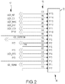
- FIG. 2 shows a schematic representation of a portion of the processor 12.
- the processor 12 includes programmable flags 19 that are labeled PF15-PFO.
- Each programmable flag 19 is associated with a processor pin 15.
- the programmable flag 19 labeled P15 is associated with pin C6.
- Programmable flag 19 labeled PF0 is associated with pin D2.
- more or fewer programmable flags 19 can be employed and pin configurations can be employed.
- the pins 15 are also shown as having corresponding signals.
- the signals shown are associated with the first accessory 20.
- the assignment of the signals to the corresponding pins 110 is a connector pin assignment 17.
- the connector pin assignment 17 is associated with the buttons 22, which are infrared, on the first accessory 20. In alternative embodiments, the connector pin assignment 17 can be associated with other accessories such as a hard drive, mechanical keyboard, display, etc.
- the connector pin assignment 17 includes signals such as CS_MAX which can be an accessory chip select signal.
- the accessory chip (not shown) can control the buttons 22.
- the BTN_DATx can be data from the buttons 22 such as a signal indicating the corresponding button is pressed. These and othersignals are shown in the following table. Assignment Signal CS_ MAX MAX chip select. BTN_DAT Data for IR buttons. BTN_DAT0 Data for button 1. BTN_DAT1 Data for button 2. 3.3V_ FB Power supply.
- LCD_ CS LCD chip select SCK Serial clock for serial communication MOSI Master Output Slave Input. Serial output for master and input for slave. LCD_A0 Indicates that registers on MAX chip are display data. LCD_RES LCD reset. PWM_IR Provides a clock for the MAX chip. FB_LED Control button feedback LED. CS_ EEPROM EEPROM chip select. MISO Master Input Slave Output. Serial input for master and output for slave.
- programmable flags 19 can be configured during the initialization of the processor board 10. Accordingly, the processor 12 is configured with the connector pin assignment 17, which can be compatible with the first accessory 20, as discussed in more detail in the following.
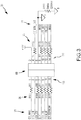
- FIG. 3 shows a schematic representation of the first accessory 20.
- the connector 100 is shown with the exemplary connector pin assignment 17 described with reference to FIG. 2 .
- the connector 100 includes the plurality of pins 110 numbered 1-14 although other connectors can be employed in alternative embodiments.
- each of the signals is associated with one of the pins110 on the connector 100.
- the set of signals being assigned to the plurality of pins 110 is an accessory pin assignment 21.
- all of the pins 110 on the connector 100 are assigned to a signal. Accordingly, none of the pins 110 are available for additionally neededsignals.
- the connector pin assignment 17 is configured as shown in FIG. 2 .
- the connector pin assignment 17 can be reconfigured when a different accessory is coupled to the connector 100, as will be described in more detail in the following.
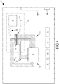
- FIG. 4 shows anothertop plan view of the processor board 10 with the connector 100 according to an embodiment.
- a second accessory 30 is coupled to the processor board 10.
- the connector pin assignment 17 in the processor board 10 can be changed to be compatible with the second accessory 30.
- the second accessory 30 includes an accessory memory 34 and buttons 32.
- the second accessory buttons 32 are different than the buttons 22 on the first accessory 20.
- the buttons 22 on the first accessory 20 may be infrared buttons.
- the buttons 32 on the second accessory 30 might be capacitive touch buttons.
- the difference between the two button types can include different data protocol, number of pins needed, voltage required, etc. These and other differences between the buttons 22, 32 can require changing the connector pin assignments 17.
- FIG. 5 shows a schematic representation of another accessory 30 according to an embodiment.
- the set of signals being assigned to the plurality of pins 110 is a second accessory pin assignment 31.
- the first and the second accessory pin assignments 21, 31 have some commonly assigned pins.
- the MISO signal is assigned to pin 14 in both the first and the second accessory pin assignments 21, 31.
- Other pins are commonly assigned.
- These commonly assigned pins can be employed to initialize and read data from the accessories 20, 30 even though the connector pin assignment 17 has not been changed.
- the data read can include data associated with the second accessory 30. Using this data, the connector pin assignment 17 can be changed to be compatible with the accessory pin assignment 31. In the embodiment shown in FIGS. 4 and 5 , the connector pin assignment 17 is changed after the second accessory 30is coupled to the connector 100.
- the connector pin assignment 17 can be changed by reassigning some of the connector pins 110.
- pins 1, 2, and 4 were reassigned. More specifically, pin 1 was reassigned from the CS_MAX signal to the BTN_DAT0 signal.
- Pin 2 was assigned from voltage supply +14V to BTN_DAT1.
- Pin 4 was reassigned from BTN_DAT to BTN_DAT2.
- Pins that were not reassigned include the PWM_IR and the SCK pins.
- the connector pin assignment 17 can be changed by reprogramming the programmable flags 19 that are associated with each pin 15 on the processor 12. The method and apparatus for reconfiguring the pin assignments on the connector 100 are described in more detail in the following with reference to FIGS. 6 and 7 .
- FIG. 6 shows a block diagram representation of an apparatus 600 for reconfiguring the pinassignments on the connector 100.
- the apparatus 600 for reconfiguring the pin assignments includes the processor board 10 and the second accessory 30.
- the processor board 10 includes the processor 12, the memory 18, and the programmable flags 19.
- the memory 18 is shown as having a database DB.
- the database DB includes a stored accessory type 18a, stored flag 18b, and stored accessory data 18c.
- the accessory memory 34 in the second accessory 30 includes a present accessory type 34a, a present flag 34b, and a present accessory data 34c.
- An arrow between the processor 12 and the second accessory 30 is a representation of the connector 100 according to an embodiment.
- the present accessory type 34a can be read by the processor 12 through the connector 100.
- the present accessory type34a can be a value that is associated with the type of the second accessory 30.
- the present accessory type 34a can indicate the type of button 34 that is used on the second accessory 30.
- the second accessory 30 has capacitive touch buttons 32, other button types can be employed in alternative embodiments.
- the present accessory type 34a can also indicate that the second accessory 30 has other features like a display or other I/O components. Also stored in the accessory memory 34 are the present flag 34b and the present accessory data 34c.
- the present flag 34b can be a unique identifier of the second accessory 30.
- some accessories may require calibration or testing.
- the calibration and testing can write values to the accessory memory 34 that are particular to the second accessory 30.
- the values can be calibration factors for buttons in the accessory, although capacitive touch buttons may not employ calibration factors. These and other values can be written to the accessory memory 34 as the present accessory data 34c.
- the stored accessory type and flag 18a,b can be provided by the first accessory 20 coupled to the processor board 10 before the second accessory 30.
- the stored accessory type 18a can be associated with a connector pin assignment 17 that is compatible with the first accessory 20.
- the stored flag 18b can be associated with the values, such as calibration values, that are associated with the first accessory 20.
- the first accessory 20 can be referred to as a prior accessory. In alternative embodiments, any accessory can be the prior accessory.
- the method of reconfiguring the pin assignments is illustrated with the embodiment where the first accessory 20 is the prior accessory and the second accessory 30 is coupled to the processor board 10.
- FIG. 7 shows a flow chart illustrating a method 700 of reconfiguring pin assignments on the connector 100 according to an embodiment.
- the method 700 includes initializing the database 702, initializing the accessory 704, and an accessory type check 706. After the accessory type check 706, a write new type 708 or a flag check 710 can occur. An additional data check 712 can occur after the flag check 710. A write new flag 714 or a checksum 716 occurs after the additional data check 712. From the checksum 716, the method 700 can generate an error and write a new flag718 or load memory data to the database 720. The method ends at step 722.
- the initialize database 702 step can include initializing the database DB described with reference to FIG. 6 .
- the initialize database 702 can occur when the processor board 10 receives power, the software on the processor 12 issues a command to initialize the database DB, or by any other appropriate means.
- the initialize database 702 step can be comprised of checking the database DB for data, the size of the database DB, the schema, writing data to the database DB, or the like.
- the processor board 10 can include other memory, such as non-volatile memory, that stores data for the database DB when power is lost to the processor board 10.
- the initialize database 702 step can read data from the non-volatile memory and write the data into the database DB.
- the initializeaccessory 704step can occur when the second accessory 30 is coupled to the processor board 10.
- the initialize accessory 704step can also occur at other times such as when the processor board 10 is initialized or receives power.
- the initialize accessory 704 step may be comprised of providing power to the second accessory 30 through the connector 100. The power can be provided when the second accessory30 is coupled to the connector 100.
- the initialize accessory 704step can also be comprised of other routines such as hardware verifications and data integrity checks.
- the initialize accessory 704step also includes reading the present accessory type 34a from the accessory memory 34.
- the processor 12 can read the present accessory type 34a from the accessory memory 34 over a pin in the connector 100.
- the present accessory type 34a can be read through the MISO pin 14.
- pin 14 is assigned to the MISO signal in both the first and second accessory pin assignments 21, 31.
- the CS_EEPROM on pin 13 can be enabled prior to reading the present accessory type 34a from the accessory memory 34. Enabling the CS_EEPROM can allow the accessory memory 34 to be read and written to the database DB.
- the accessory type check 706 can be performed.
- the accessory type check 706 determines if the accessory type has changed. For example, the accessory type check 706 can determine if the presentaccessory type 34a is different than the stored accessory type 18a. If the types 34a, 18a are different, the accessory pin assignment 31 might not be compatible with the connector pin assignment 17. In the exemplary embodiments described in the foregoing, the accessory pin assignments 31, 21 are different and incompatible. Accordingly, when the second accessory 30 is coupled to the processor board 10, the second accessory pin assignment 31 is not compatible with the connector pin assignment 17.
- the write new type 708 step occurs if the accessory type check 706 indicates that the accessory type is different.
- the new type can be the present accessory type 34a read from the accessory memory 34 and written to the database DB.
- the processor board 10 can read the present accessory type 34a from the accessory memory 34 through the connector 100.
- the connector pin assignment 17 might be incompatible with the accessory pin assignment 31, the two configurations can still have commonly assigned pins.As discussed in the foregoing, these commonly assigned pins can be employed to read data, such as the accessory type, from the second accessory memory 34.
- the flag check 710 occurs if the accessory type check 706 indicates that the accessory type has not changed.
- the present flag 34b is compared with the stored flag 18b. If the comparison indicates that the stored flag 18b has not changed, then the method ends. Accordingingly, if the second accessory 30 has an accessory pin assignment31 that is compatible with the connector pin assignment 17, then the method does not write the new type to the database DB and the stored flag 18b is not changed. If the comparison between the stored flag 18b and the present flag 34bare different, then the method 700 executes an additional data check 712.
- the first and second accessories can be the same type but have different flags.
- the first and the second accessories could be IR button types with different calibration values. Accordingly, the first and second accessories are the same type of accessory but have a present flag that is different than the stored flag.
- the calibration or other values stored in the present accessory data 34c may need to be read from the accessory memory 34 and written to the database DB. This decision is made in the additional data check 712.
- the additional data check 712 can follow the write new type 708 step or the flag check 710.
- the additional data check 712 determines if additional data is required from the accessory memory 34.
- the second accessory 30 can, in some embodiments,have data that needs to be written to the database DB. In the embodiment where the second accessory 30 is a capacitive touch button type, additional data may not be required. In other embodiments, the additional data check can check if the type is associated with having calibration values. If the additional data check 712 indicates that additional data is not necessary, the method may write a new flag to the database714 and end 722.
- the checksum 716 step verifies the integrity of the data in the accessory memory 34. If the checksum 716 verifies the integrity of the data, the load memory data to database 720 step can execute.
- the additional data can be loaded into the database DB through the connector 100. In alternative embodiments, the additional data can be loaded through other communications means.
- the embodiments described above provide a method 700 and apparatus 600 for reconfiguring the pin assignments on a connector 100.
- the method 700 and apparatus600 can read the present accessory type 34a from the second accessory 30.
- the method can use the present accessory type 34a to determine if the connector pin assignment 17 is not compatible with the accessory pin assignment 31.
- the method 700 and apparatus 600 can reconfigure the connector pin assignment 17 to be compatible with the second accessory pin assignment 31.
- the accessory pin assignment 31 When the second accessory 30 is coupled to the processor board 10, the accessory pin assignment 31 might not be compatible with the connector pin assignment 17. However, the accessory pin assignment 31 can have pins that are commonly assigned with the connector pin assignment 17, including pins that provide power to the second accessory 30. Accordingly, even if the accessory pin assignment 31 is not compatible with the connector pin assignment 17, the second accessory 30 can be initialized and data can be read from the accessory memory 34.
- the data can include the present accessory type 34a, present flag 34b, and the present accessory data 34c.
- the present accessory type 34a, present flag 34b, and the present accessory data 34c can be read through commonly assigned pins on the connector 100. Accordingly, the connector pin assignment 17 can be configured for the first accessory 20 and still provide data to the processor board 10 to change the connector pin assignment 17. Accordingly, the pin assignments on the connector 100 can be reconfigured even if the connector 100 has pins already assigned for a particular type of accessory.
Landscapes
- Engineering & Computer Science (AREA)
- Theoretical Computer Science (AREA)
- General Engineering & Computer Science (AREA)
- Physics & Mathematics (AREA)
- General Physics & Mathematics (AREA)
- Computer Hardware Design (AREA)
- Details Of Connecting Devices For Male And Female Coupling (AREA)
- Microcomputers (AREA)
- Dental Tools And Instruments Or Auxiliary Dental Instruments (AREA)
Description
- The embodiments described below relate to connectors with pin assignments and, more particularly, to a method and apparatus for reconfiguring pin assignments on a connector.
- Electronic devices communicate with each other through connectors. For example, a printed circuit board(PCB) can have a multi-pin connector that is soldered to the board. The connector can interface with a cable so that each exposed conductor in the cable can electrically couple with each pin in the connector. The electronic device can communicate through the connector and cable by sending and receiving signals through the pins and conductors. The connector is typically keyed so the cable cannot be installed backwards into the connector. Sometimes, instead of a cable, the PCB can be coupled directly to another PCB. For example, input/output (I/O) devices with integrated displays and keyboards are sometimes coupled to processor boards through a mating pair connector. Similar to the connector to cable arrangement, each pin in the mating pair connector are uniquely paired with another pin in the connector.
- The connectors on the PCB have pin assignments. That is, each pin in the connectors on the PCB is assigned to a specific signal. The assignments can include signals that, for example, provide+5VDC to an I/O device, receive data from the I/O to the processor board (typically denoted as 'DATA'), interrupt a transmission through the connector, etc. To ensure interoperability of various PCBs, many standards, such as the RS-232 standard, have been developed that specify which pin in the connector is allocated to a particular signal. Although some of the standards do not assign all of the pins to a signal, such unassigned pins are oftentimes used for a proprietarysignal. As a result, some connectors are not compatible even if in technical compliance with a standard.
- General purpose input and output (GPIO) connectors are also employed in many electronic devices. These connectors are able to interface with peripheral devices over several different standards. However, the connectors, due to interfacing with the different standards, are usually large and bulky and must be designed into the product. For example, a few pins might be assigned exclusively to the USB protocol whereas the other pins are assigned to SCSI or PCM protocols. Also, the GPIO connectors rely on the standards with known pin assignments rather than proprietary pin assignments that are associated with particular electronic devices.
- Many PCBs employ connectors with wholly proprietary pin assignments. Concerns such as space, costs, form factor constraints, weight, licensing considerations, and minimum data rates can induce manufacturers to use proprietary pin assignments. For example, a company may develop a unique pin assignment for a custom processor board that must fit within a confined space in a product. Commonly available boards with GPIO or industry standard connectors might be too costly or too large to fit within the product. Accordingly, companies have developed proprietary pin assignments that fully utilized all of the pins on small connectors.
- The connectors with such proprietary pin assignments are sometimes used between devices that require upgrades or replacements. For example, a processor board with a proprietary pin assignment to an I/O connector may not be a candidate for an upgrade due to the customer's reliance on the board's processor version. However, the I/O device coupled to the I/O connector might be upgraded due to technological progress in sensors. For example, infrared buttons might be replaced by capacitive touch buttons if the capacitive touch buttons are less expensive or more reliable for a particular application.
- These upgrades may require different pin assignments to work properly with the processor boards. However, the connectors have pins already assigned for a particular type of accessory.Accordingly, there is a need for an apparatus and a method of reconfiguring pin assignments on a connector.
-
US7865629 discloses to reconfigure pin assignments based on configuration information provided by the accessory. - The scope of protection is defined by the appended claims.
- The same reference number represents the same element on all drawings. It should be understood that the drawings are not necessarily to scale.
-
FIG. 1 shows a plan view of aprocessor board 10 according to an embodiment. -
FIG. 2 shows a schematic representation of a portion of theprocessor 12. -
FIG. 3 shows a schematic representation of thefirst accessory 20. -
FIG. 4 shows another top plan view of theprocessor board 10 with theconnector 100 according to an embodiment. -
FIG. 5 shows a schematic representation of anotheraccessory 30 according to an embodiment. -
FIG. 6 shows a block diagram representation of anapparatus 600 for reconfiguring the pin assignments on theconnector 100. -
FIG. 7 shows a flow chart illustrating amethod 700 of reconfiguring pin assignments on theconnector 100 according to an embodiment. -
FIG. 1 shows a plan view of aprocessor board 10 according to an embodiment. As shown, theprocessor board 10 includes aconnector 100 that is coupled to a substrate on theprocessor board 10. Theconnector 100 is a mating pair with only the female half of the pair shown. The male portion is not shown for clarity. Theprocessor board 10 also includes aprocessor 12, a plurality ofcommunication ports 14a, 14b, acommunications chip 16, andmemory 18. However, different configurations can be employed in alternative embodiments. As can be seen, theconnector 100 is coupled to theprocessor 12 via pathways 13 (all the pathways are not shown for clarity). Thepathways 13 couple pins on theprocessor 12topins 110 on theconnector 100. Each of thepathways 13 carry signals that are related to a particular function. Theprocessor 12 has programmable flags that can be configured to associate a signal to aparticular pin 15 on theprocessor 12. - Also shown is a
first accessory 20 that is coupled to theprocessor board 10 via theconnector 100. Thefirst accessory 20 is shown in transparent view for clarity. In the embodiment shown, thefirst accessory 20 includes anaccessory memory 24 andbuttons 22. Thebuttons 22 may be infrared buttons although any suitable input device can be employed in alternative embodiments. Thefirstaccessory 20 can also have different configurations and perform different functions. For example, although thefirst accessory 20 is an I/O device, in alternative embodiments, thefirst accessory 20 can be any device such as a display, a second processor board, communications board, memory card, or the like. Thebuttons 22 and accessory memory 24are coupled to theconnector 100 via pathways (not shown). In alternative embodiments, the buttons22and accessory memory 24 can be coupled to theconnector 100 through an interface, buffer, or the like. - The
accessory memory 24 is anEEPROM that is adapted to store data although any suitable memory for storing the data can be employed in alternative embodiments. The data can beassociated with thefirst accessory 20. For example, the data could indicate that thefirst accessory 20 has theinfrared buttons 22. Theaccessory memory 24 can also provide the data to another device such as theprocessor 12. Theprocessor 12 can receive that data from theaccessory memory 24 through theconnector 100. Additionally or alternatively, the data can be provided through a second connector, a wireless communication, an optocoupler, or the like. -
FIG. 2 shows a schematic representation of a portion of theprocessor 12. As can be seen, theprocessor 12 includesprogrammable flags 19 that are labeled PF15-PFO. Eachprogrammable flag 19 is associated with aprocessor pin 15. For example, theprogrammable flag 19 labeled P15 is associated with pin C6.Programmable flag 19 labeled PF0 is associated with pin D2. In alternative embodiments, more or fewerprogrammable flags 19 can be employed and pin configurations can be employed. Thepins 15 are also shown as having corresponding signals. The signals shown are associated with thefirst accessory 20. The assignment of the signals to the correspondingpins 110 is aconnector pin assignment 17. - In the embodiment shown, the
connector pin assignment 17 is associated with thebuttons 22, which are infrared, on thefirst accessory 20. In alternative embodiments, theconnector pin assignment 17 can be associated with other accessories such as a hard drive, mechanical keyboard, display, etc. Theconnector pin assignment 17 includes signals such as CS_MAX which can be an accessory chip select signal. The accessory chip (not shown) can control thebuttons 22. The BTN_DATx can be data from thebuttons 22 such as a signal indicating the corresponding button is pressed. These and othersignals are shown in the following table.Assignment Signal CS_ MAX MAX chip select. BTN_DAT Data for IR buttons. BTN_DAT0 Data for button 1.BTN_DAT1 Data for button 2.3.3V_ FB Power supply. LCD_ CS LCD chip select. SCK Serial clock for serial communication MOSI Master Output Slave Input. Serial output for master and input for slave. LCD_A0 Indicates that registers on MAX chip are display data. LCD_RES LCD reset. PWM_IR Provides a clock for the MAX chip. FB_LED Control button feedback LED. CS_ EEPROM EEPROM chip select. MISO Master Input Slave Output. Serial input for master and output for slave. - In an embodiment,
programmable flags 19 can be configured during the initialization of theprocessor board 10. Accordingly, theprocessor 12 is configured with theconnector pin assignment 17, which can be compatible with thefirst accessory 20, as discussed in more detail in the following. -
FIG. 3 shows a schematic representation of thefirst accessory 20. Theconnector 100 is shown with the exemplaryconnector pin assignment 17 described with reference toFIG. 2 . Theconnector 100 includes the plurality ofpins 110 numbered 1-14 although other connectors can be employed in alternative embodiments. As can be seen, each of the signals is associated with one of the pins110 on the connector 100.The set of signals being assigned to the plurality ofpins 110 is anaccessory pin assignment 21. As can be appreciated, all of thepins 110 on theconnector 100 are assigned to a signal. Accordingly, none of thepins 110 are available for additionally neededsignals. To be compatible with theaccessory pin assignment 21, theconnector pin assignment 17 is configured as shown inFIG. 2 . Theconnector pin assignment 17 can be reconfigured when a different accessory is coupled to theconnector 100, as will be described in more detail in the following. -
FIG. 4 shows anothertop plan view of theprocessor board 10 with theconnector 100 according to an embodiment. Instead of thefirst accessory 20, asecond accessory 30 is coupled to theprocessor board 10. In an embodiment, theconnector pin assignment 17 in theprocessor board 10 can be changed to be compatible with thesecond accessory 30. Similar to thefirst accessory 20, thesecond accessory 30 includes anaccessory memory 34 andbuttons 32. However, the secondaccessory buttons 32 are different than thebuttons 22 on thefirst accessory 20. For example, thebuttons 22 on thefirst accessory 20 may be infrared buttons. Thebuttons 32 on thesecond accessory 30 might be capacitive touch buttons. The difference between the two button types can include different data protocol, number of pins needed, voltage required, etc. These and other differences between thebuttons connector pin assignments 17. -
FIG. 5 shows a schematic representation of another accessory 30 according to an embodiment. The set of signals being assigned to the plurality ofpins 110 is a secondaccessory pin assignment 31. As can be appreciated when comparingFIG. 5 withFIG. 3 , the first and the secondaccessory pin assignments accessory pin assignments accessories connector pin assignment 17 has not been changed. The data read can include data associated with thesecond accessory 30. Using this data, theconnector pin assignment 17 can be changed to be compatible with theaccessory pin assignment 31. In the embodiment shown inFIGS. 4 and5 , theconnector pin assignment 17 is changed after the second accessory 30is coupled to theconnector 100. - The
connector pin assignment 17 can be changed by reassigning some of the connector pins 110. In the embodiments of the first andsecond accessories pin 1 was reassigned from the CS_MAX signal to the BTN_DAT0 signal.Pin 2 was assigned from voltage supply +14V to BTN_DAT1.Pin 4 was reassigned from BTN_DAT to BTN_DAT2. Pins that were not reassigned include the PWM_IR and the SCK pins. Theconnector pin assignment 17 can be changed by reprogramming theprogrammable flags 19 that are associated with eachpin 15 on theprocessor 12. The method and apparatus for reconfiguring the pin assignments on theconnector 100 are described in more detail in the following with reference toFIGS. 6 and7 . -
FIG. 6 shows a block diagram representation of anapparatus 600 for reconfiguring the pinassignments on theconnector 100. In the embodiment shown, theapparatus 600 for reconfiguring the pin assignments includes theprocessor board 10 and thesecond accessory 30. Theprocessor board 10 includes theprocessor 12, thememory 18, and theprogrammable flags 19. Thememory 18 is shown as having a database DB. The database DB includes a storedaccessory type 18a, storedflag 18b, and storedaccessory data 18c. Theaccessory memory 34 in thesecond accessory 30 includes apresent accessory type 34a, apresent flag 34b, and apresent accessory data 34c. An arrow between theprocessor 12 and thesecond accessory 30 is a representation of theconnector 100 according to an embodiment. Thepresent accessory type 34a can be read by theprocessor 12 through theconnector 100. - The present accessory type34a can be a value that is associated with the type of the
second accessory 30. For example, in an embodiment, thepresent accessory type 34a can indicate the type ofbutton 34 that is used on thesecond accessory 30. Although thesecond accessory 30 hascapacitive touch buttons 32, other button types can be employed in alternative embodiments. Thepresent accessory type 34a can also indicate that thesecond accessory 30 has other features like a display or other I/O components. Also stored in theaccessory memory 34 are thepresent flag 34b and thepresent accessory data 34c. - The
present flag 34b can be a unique identifier of thesecond accessory 30. For example, some accessories may require calibration or testing. The calibration and testing can write values to theaccessory memory 34 that are particular to thesecond accessory 30. The values can be calibration factors for buttons in the accessory, although capacitive touch buttons may not employ calibration factors. These and other values can be written to theaccessory memory 34 as thepresent accessory data 34c. - In the embodiments shown, the stored accessory type and
flag 18a,bcan be provided by thefirst accessory 20 coupled to theprocessor board 10 before thesecond accessory 30. For example, prior to initializing thesecond accessory 30, the storedaccessory type 18a can be associated with aconnector pin assignment 17 that is compatible with thefirst accessory 20. The storedflag 18b can be associated with the values, such as calibration values, that are associated with thefirst accessory 20. In the embodiments described in the foregoing, thefirst accessory 20 can be referred to as a prior accessory. In alternative embodiments, any accessory can be the prior accessory. The method of reconfiguring the pin assignments is illustrated with the embodiment where thefirst accessory 20 is the prior accessory and thesecond accessory 30 is coupled to theprocessor board 10. -
FIG. 7 shows a flow chart illustrating amethod 700 of reconfiguring pin assignments on theconnector 100 according to an embodiment. Themethod 700 includes initializing thedatabase 702, initializing theaccessory 704, and anaccessory type check 706. After theaccessory type check 706, a writenew type 708 or aflag check 710 can occur. An additional data check 712 can occur after theflag check 710. A writenew flag 714 or achecksum 716 occurs after the additional data check 712. From thechecksum 716, themethod 700 can generate an error and write a new flag718 or load memory data to thedatabase 720. The method ends atstep 722. - The
initialize database 702 step can include initializing the database DB described with reference toFIG. 6 . Theinitialize database 702 can occur when theprocessor board 10 receives power, the software on theprocessor 12 issues a command to initialize the database DB, or by any other appropriate means. Theinitialize database 702 step can be comprised of checking the database DB for data, the size of the database DB, the schema, writing data to the database DB, or the like. For example, theprocessor board 10 can include other memory, such as non-volatile memory, that stores data for the database DB when power is lost to theprocessor board 10. Theinitialize database 702 step can read data from the non-volatile memory and write the data into the database DB. - The initializeaccessory 704step can occur when the
second accessory 30 is coupled to theprocessor board 10. The initialize accessory 704step can also occur at other times such as when theprocessor board 10 is initialized or receives power. Theinitialize accessory 704 step may be comprised of providing power to thesecond accessory 30 through theconnector 100. The power can be provided when the second accessory30 is coupled to theconnector 100. The initialize accessory 704step can also be comprised of other routines such as hardware verifications and data integrity checks. - The initialize accessory 704step also includes reading the
present accessory type 34a from theaccessory memory 34. Theprocessor 12 can read thepresent accessory type 34a from theaccessory memory 34 over a pin in theconnector 100. For example, in the embodiments of theconnector 100 described in the foregoing, thepresent accessory type 34a can be read through theMISO pin 14. As discussed in the foregoing,pin 14 is assigned to the MISO signal in both the first and secondaccessory pin assignments pin 13 can be enabled prior to reading thepresent accessory type 34a from theaccessory memory 34. Enabling the CS_EEPROM can allow theaccessory memory 34 to be read and written to the database DB.After theinitialize database 702 and initializeaccessory 704 steps, the accessory type check 706 can be performed. - The accessory type check 706determines if the accessory type has changed. For example, the accessory type check 706 can determine if the
presentaccessory type 34a is different than the storedaccessory type 18a. If thetypes accessory pin assignment 31 might not be compatible with theconnector pin assignment 17. In the exemplary embodiments described in the foregoing, theaccessory pin assignments second accessory 30 is coupled to theprocessor board 10, the secondaccessory pin assignment 31 is not compatible with theconnector pin assignment 17. - The write
new type 708 step occurs if theaccessory type check 706 indicates that the accessory type is different. The new type can be thepresent accessory type 34a read from theaccessory memory 34 and written to the database DB. For example, theprocessor board 10 can read thepresent accessory type 34a from theaccessory memory 34 through theconnector 100. Although theconnector pin assignment 17 might be incompatible with theaccessory pin assignment 31, the two configurations can still have commonly assigned pins.As discussed in the foregoing, these commonly assigned pins can be employed to read data, such as the accessory type, from thesecond accessory memory 34. - The
flag check 710 occurs if theaccessory type check 706 indicates that the accessory type has not changed. During theflag check 710, thepresent flag 34b is compared with the storedflag 18b. If the comparison indicates that the storedflag 18b has not changed, then the method ends.Accordingly, if thesecond accessory 30 has an accessory pin assignment31 that is compatible with theconnector pin assignment 17, then the method does not write the new type to the database DB and the storedflag 18b is not changed. If the comparison between the storedflag 18b and the present flag 34bare different, then themethod 700 executes an additional data check 712. - In some embodiments, the first and second accessories can be the same type but have different flags. For example, in alternative embodiments, the first and the second accessories could be IR button types with different calibration values. Accordingly, the first and second accessories are the same type of accessory but have a present flag that is different than the stored flag. The calibration or other values stored in the
present accessory data 34c may need to be read from theaccessory memory 34 and written to the database DB. This decision is made in the additional data check 712. - The additional data check 712 can follow the write
new type 708 step or theflag check 710. The additional data check 712 determines if additional data is required from theaccessory memory 34. For example, thesecond accessory 30 can, in some embodiments,have data that needs to be written to the database DB. In the embodiment where thesecond accessory 30 is a capacitive touch button type, additional data may not be required. In other embodiments, the additional data check can check if the type is associated with having calibration values. If the additional data check 712 indicates that additional data is not necessary, the method may write a new flag to the database714 and end 722. - If additional data is needed, the
checksum 716 step verifies the integrity of the data in the accessory memory 34.If thechecksum 716 verifies the integrity of the data, the load memory data todatabase 720 step can execute. The additional data can be loaded into the database DB through theconnector 100. In alternative embodiments, the additional data can be loaded through other communications means. - The embodiments described above provide a
method 700 andapparatus 600 for reconfiguring the pin assignments on aconnector 100. As explain above, themethod 700 and apparatus600 can read thepresent accessory type 34a from the second accessory 30.The method can use thepresent accessory type 34a to determine if theconnector pin assignment 17 is not compatible with theaccessory pin assignment 31. Themethod 700 andapparatus 600 can reconfigure theconnector pin assignment 17 to be compatible with the secondaccessory pin assignment 31. - When the
second accessory 30 is coupled to theprocessor board 10, theaccessory pin assignment 31 might not be compatible with theconnector pin assignment 17. However, theaccessory pin assignment 31 can have pins that are commonly assigned with theconnector pin assignment 17, including pins that provide power to thesecond accessory 30. Accordingly, even if theaccessory pin assignment 31 is not compatible with theconnector pin assignment 17, thesecond accessory 30 can be initialized and data can be read from theaccessory memory 34. The data can include thepresent accessory type 34a,present flag 34b, and thepresent accessory data 34c. Thepresent accessory type 34a,present flag 34b, and thepresent accessory data 34c can be read through commonly assigned pins on theconnector 100. Accordingly, theconnector pin assignment 17 can be configured for thefirst accessory 20 and still provide data to theprocessor board 10 to change theconnector pin assignment 17. Accordingly, the pin assignments on theconnector 100 can be reconfigured even if theconnector 100 has pins already assigned for a particular type of accessory.
Claims (11)
- A method (700) for reconfiguring pin assignments on a connector (100), the method comprising:reading a present accessory type (34a) from an accessory (30) coupled to the connector (100) having a plurality of pins (110) wherein the present accessory type (34a) is associated with an accessory pin assignment (31) of the connector (100);comparing the present accessory type (34a) to a stored accessory type (18a) associated with a connector pin assignment (17) to determine if the accessory pin assignment (31) is compatible with the connector pin assignment (17);wherein the stored accessory type (18a) is associated with a prior accessory (20) coupled to the connector (100); andif the present accessory type (34a) has not changed with regard to the stored accessory type, reading a present flag (34b) from the accessory memory (34) in the accessory (30) to determine whether to perform a check if additional data in addition to the present accessory type (34a) is required from the accessory (30) to communicate with the accessory (30);changing the connector pin assignment (17) based on the comparison between the present accessory type (34a) and the stored accessory type (18a);wherein the present accessory type (34a) is read through at least one of the plurality of pins (110).
- The method of claim 1, further comprising changing the connector pin assignment (17) to be compatible with the accessory pin assignment (31) if the accessory pin assignment (31) is incompatible with the connector pin assignment (17).
- The method of claim 2, wherein changing the connector pin assignment (17) includes changing at least one data pin assignment to read data from the accessory (30) coupled to the connector (100).
- The method of claim 1, wherein the present flag (34b) is associated with calibration factors determined from calibrating the accessory (30) prior to the accessory (30) being coupled to a processor board (10).
- The method of claim 1, wherein the at least one of the plurality of pins (110) is commonly assigned in at least two accessory pin assignments (21, 31).
- An apparatus (600) for reconfiguring pin assignments on a connector (100), comprising:the connector (100) having a plurality of pins (110);an accessory (30) coupled to the connector (100); anda processor (12) coupled to the plurality of pins (110), the processor (12) being configured to:read a present accessory type (34a) from the accessory (30) wherein the present accessory type (34a) is associated with an accessory pin assignment (31);compare the present accessory type (34a) to a stored accessory type (18a) associated with a connector pin assignment (17);wherein the stored accessory type (18a) is associated with a prior accessory (20) coupled to the connector (100);change the connector pin assignment (17) based on the comparison between the present accessory type (34a) and the stored accessory type (18a); andif the present accessory type (34a) has not changed with regard to the stored accessory type, check a present flag (34b) of the accessory to determine whether to perform a check if additional data is required from the accessory (30) to communicate with the accessory (30);wherein the present accessory type (34a) is read through at least one of the plurality of pins (110).
- The apparatus of claim 6, wherein the processor (12) is further configured to determine if the accessory pin assignment (31) is compatible with the connector pin assignment (17) based on the comparison between the present accessory type (34a) and the stored accessory type (18a).
- The apparatus of claim 6, wherein the processor (12) is further configured to change at least one data pin assignment in the connector pin assignment (17) to read data from the accessory (30).
- The apparatus of claim 6, wherein the present flag (34b) is associated with calibration factors determined from calibrating the accessory (30) prior to the accessory (30) being coupled to a processor board (10).
- The apparatus of claim 6, wherein the at least one of the plurality of pins (110) is commonly assigned in at least two accessory pin assignments (21, 31).
- The apparatus of claim 6, wherein the processor (12) is further configured to store the stored accessory type (18a) prior to the accessory (30) being connected to the connector (100).
Applications Claiming Priority (1)
| Application Number | Priority Date | Filing Date | Title |
|---|---|---|---|
| PCT/CN2014/073347 WO2015135170A1 (en) | 2014-03-13 | 2014-03-13 | A method and apparatus for reconfiguring pin assignments on a connector |
Publications (3)
| Publication Number | Publication Date |
|---|---|
| EP3117227A1 EP3117227A1 (en) | 2017-01-18 |
| EP3117227A4 EP3117227A4 (en) | 2017-11-22 |
| EP3117227B1 true EP3117227B1 (en) | 2021-06-16 |
Family
ID=54070802
Family Applications (1)
| Application Number | Title | Priority Date | Filing Date |
|---|---|---|---|
| EP14885760.0A Active EP3117227B1 (en) | 2014-03-13 | 2014-03-13 | A method and apparatus for reconfiguring pin assignments on a connector |
Country Status (6)
| Country | Link |
|---|---|
| US (1) | US10430365B2 (en) |
| EP (1) | EP3117227B1 (en) |
| JP (1) | JP6449319B2 (en) |
| CN (1) | CN106062573B (en) |
| AR (1) | AR099702A1 (en) |
| WO (1) | WO2015135170A1 (en) |
Families Citing this family (4)
| Publication number | Priority date | Publication date | Assignee | Title |
|---|---|---|---|---|
| US9736531B2 (en) | 2015-09-08 | 2017-08-15 | Google Inc. | Video media streaming device |
| US10277275B2 (en) | 2015-09-08 | 2019-04-30 | Google Llc | Audio media streaming device |
| US10073752B2 (en) * | 2016-01-13 | 2018-09-11 | Bby Solutions, Inc. | Universal smart connection pad |
| JP7139815B2 (en) * | 2018-09-19 | 2022-09-21 | 富士フイルムビジネスイノベーション株式会社 | Information processing equipment |
Family Cites Families (17)
| Publication number | Priority date | Publication date | Assignee | Title |
|---|---|---|---|---|
| JPH05189303A (en) * | 1992-01-14 | 1993-07-30 | Matsushita Electric Ind Co Ltd | Information processor |
| TW548414B (en) * | 2002-01-29 | 2003-08-21 | Via Tech Inc | Automatic integrated circuit overall machine testing system, apparatus and its method |
| US7050783B2 (en) * | 2002-02-22 | 2006-05-23 | Kyocera Wireless Corp. | Accessory detection system |
| JP2004029963A (en) * | 2002-06-21 | 2004-01-29 | Canon Inc | Interface device for device connection |
| JP2006350451A (en) * | 2005-06-13 | 2006-12-28 | Sharp Corp | Circuit design support device and circuit design support method |
| US20080140323A1 (en) * | 2006-12-07 | 2008-06-12 | Fujitsu Limited | Check support apparatus and computer product |
| US7958276B2 (en) * | 2007-01-22 | 2011-06-07 | Counterpath Corporation | Automatic configuration of peripheral devices |
| US8365201B2 (en) * | 2007-12-14 | 2013-01-29 | Microsoft Corporation | Multi-function device ID with unique identifier |
| US8208853B2 (en) * | 2008-09-08 | 2012-06-26 | Apple Inc. | Accessory device authentication |
| CN101738503B (en) * | 2008-11-18 | 2011-10-05 | 中芯国际集成电路制造(上海)有限公司 | Interface device and control method and aging test system thereof |
| CN102043100B (en) * | 2009-10-09 | 2013-03-06 | 中芯国际集成电路制造(上海)有限公司 | Aging test system |
| US7865629B1 (en) | 2009-11-24 | 2011-01-04 | Microsoft Corporation | Configurable connector for system-level communication |
| JP4944213B2 (en) * | 2010-01-04 | 2012-05-30 | 株式会社バッファロー | Main device, external device, and communication system |
| KR101854929B1 (en) * | 2010-04-14 | 2018-05-04 | 마이크로소프트 테크놀로지 라이센싱, 엘엘씨 | Dynamic configuration of connectors for system level communications |
| US20110264825A1 (en) * | 2010-04-23 | 2011-10-27 | Adrian Joseph Stagg | Port sharing on a computing device |
| US8629580B2 (en) * | 2011-02-09 | 2014-01-14 | Apple Inc. | Audio accessory type detection and connector pin signal assignment |
| US9293876B2 (en) | 2011-11-07 | 2016-03-22 | Apple Inc. | Techniques for configuring contacts of a connector |
-
2014
- 2014-03-13 CN CN201480077129.0A patent/CN106062573B/en active Active
- 2014-03-13 EP EP14885760.0A patent/EP3117227B1/en active Active
- 2014-03-13 WO PCT/CN2014/073347 patent/WO2015135170A1/en not_active Ceased
- 2014-03-13 JP JP2016557069A patent/JP6449319B2/en active Active
- 2014-03-13 US US15/119,781 patent/US10430365B2/en active Active
-
2015
- 2015-03-09 AR ARP150100703A patent/AR099702A1/en unknown
Non-Patent Citations (1)
| Title |
|---|
| None * |
Also Published As
| Publication number | Publication date |
|---|---|
| JP6449319B2 (en) | 2019-01-09 |
| CN106062573A (en) | 2016-10-26 |
| EP3117227A1 (en) | 2017-01-18 |
| EP3117227A4 (en) | 2017-11-22 |
| AR099702A1 (en) | 2016-08-10 |
| US10430365B2 (en) | 2019-10-01 |
| US20170052918A1 (en) | 2017-02-23 |
| JP2017509994A (en) | 2017-04-06 |
| WO2015135170A1 (en) | 2015-09-17 |
| CN106062573B (en) | 2020-02-28 |
Similar Documents
| Publication | Publication Date | Title |
|---|---|---|
| US8886513B2 (en) | Embedded bus emulation | |
| US7287703B2 (en) | Removable memory cards including USB and other controllers, connectors, and methods of operating same | |
| CN102004522A (en) | motherboard | |
| US10430365B2 (en) | Method and apparatus for reconfiguring pin assignments on a connector | |
| CN102342042B (en) | Optical communication module and optical communication system using the optical communication module | |
| CN103914167B (en) | Computer system and touch control and display data transmission device and method thereof | |
| CN201374055Y (en) | Computer system initiatively distinguishing mainboard | |
| WO2016033518A1 (en) | Connector with in-circuit programming | |
| CN119862147A (en) | Method and device for intelligently identifying server configuration and adaptively configuring PCIe bandwidth | |
| US7123937B2 (en) | Programmable wireless transceiving module | |
| CN115078970A (en) | Chip Test System | |
| CN101751366A (en) | Mainboard with shared signal transmission interface | |
| US20100049901A1 (en) | Memory card and non-volatile memory controller thereof | |
| EP3182295A1 (en) | Communication system with serial ports for automatically identifying device types and communication protocols and method thereof | |
| CN204695749U (en) | Automatic identification and mate circuit and the liquid crystal indicator of multiple screen | |
| US12328821B2 (en) | Methods and apparatuses for interfacing microwave circuits | |
| HK1230724A1 (en) | A method and apparatus for reconfiguring pin assignments on a connector | |
| HK1230724B (en) | A method and apparatus for reconfiguring pin assignments on a connector | |
| KR102224914B1 (en) | Computer automatic assembly system | |
| US20120307438A1 (en) | Electronic device having multifunctional network interface port | |
| US20090138692A1 (en) | Self describing line cards in network switch | |
| US8634186B2 (en) | Non-volatile memory controller cable arrangement | |
| US20050180101A1 (en) | Portable storage device with interchangeable connector | |
| CN114938243A (en) | Method and system for debugging BOSA (business-oriented architecture), debugging instrument and debugging method | |
| CN108205444A (en) | A kind of efficient CTP burning programs test processes system |
Legal Events
| Date | Code | Title | Description |
|---|---|---|---|
| STAA | Information on the status of an ep patent application or granted ep patent |
Free format text: STATUS: THE INTERNATIONAL PUBLICATION HAS BEEN MADE |
|
| PUAI | Public reference made under article 153(3) epc to a published international application that has entered the european phase |
Free format text: ORIGINAL CODE: 0009012 |
|
| STAA | Information on the status of an ep patent application or granted ep patent |
Free format text: STATUS: REQUEST FOR EXAMINATION WAS MADE |
|
| 17P | Request for examination filed |
Effective date: 20161013 |
|
| AK | Designated contracting states |
Kind code of ref document: A1 Designated state(s): AL AT BE BG CH CY CZ DE DK EE ES FI FR GB GR HR HU IE IS IT LI LT LU LV MC MK MT NL NO PL PT RO RS SE SI SK SM TR |
|
| AX | Request for extension of the european patent |
Extension state: BA ME |
|
| DAX | Request for extension of the european patent (deleted) | ||
| RIN1 | Information on inventor provided before grant (corrected) |
Inventor name: WANG, LINGJUN |
|
| A4 | Supplementary search report drawn up and despatched |
Effective date: 20171019 |
|
| RIC1 | Information provided on ipc code assigned before grant |
Ipc: G01R 1/02 20060101ALI20171013BHEP Ipc: G01R 31/00 20060101AFI20171013BHEP Ipc: G06F 13/40 20060101ALI20171013BHEP Ipc: G06F 13/38 20060101ALI20171013BHEP |
|
| STAA | Information on the status of an ep patent application or granted ep patent |
Free format text: STATUS: EXAMINATION IS IN PROGRESS |
|
| 17Q | First examination report despatched |
Effective date: 20190527 |
|
| GRAP | Despatch of communication of intention to grant a patent |
Free format text: ORIGINAL CODE: EPIDOSNIGR1 |
|
| STAA | Information on the status of an ep patent application or granted ep patent |
Free format text: STATUS: GRANT OF PATENT IS INTENDED |
|
| INTG | Intention to grant announced |
Effective date: 20210112 |
|
| GRAS | Grant fee paid |
Free format text: ORIGINAL CODE: EPIDOSNIGR3 |
|
| GRAA | (expected) grant |
Free format text: ORIGINAL CODE: 0009210 |
|
| STAA | Information on the status of an ep patent application or granted ep patent |
Free format text: STATUS: THE PATENT HAS BEEN GRANTED |
|
| AK | Designated contracting states |
Kind code of ref document: B1 Designated state(s): AL AT BE BG CH CY CZ DE DK EE ES FI FR GB GR HR HU IE IS IT LI LT LU LV MC MK MT NL NO PL PT RO RS SE SI SK SM TR |
|
| REG | Reference to a national code |
Ref country code: GB Ref legal event code: FG4D |
|
| REG | Reference to a national code |
Ref country code: CH Ref legal event code: EP |
|
| REG | Reference to a national code |
Ref country code: DE Ref legal event code: R096 Ref document number: 602014078210 Country of ref document: DE |
|
| REG | Reference to a national code |
Ref country code: AT Ref legal event code: REF Ref document number: 1402780 Country of ref document: AT Kind code of ref document: T Effective date: 20210715 |
|
| REG | Reference to a national code |
Ref country code: IE Ref legal event code: FG4D |
|
| REG | Reference to a national code |
Ref country code: LT Ref legal event code: MG9D |
|
| PG25 | Lapsed in a contracting state [announced via postgrant information from national office to epo] |
Ref country code: HR Free format text: LAPSE BECAUSE OF FAILURE TO SUBMIT A TRANSLATION OF THE DESCRIPTION OR TO PAY THE FEE WITHIN THE PRESCRIBED TIME-LIMIT Effective date: 20210616 Ref country code: FI Free format text: LAPSE BECAUSE OF FAILURE TO SUBMIT A TRANSLATION OF THE DESCRIPTION OR TO PAY THE FEE WITHIN THE PRESCRIBED TIME-LIMIT Effective date: 20210616 Ref country code: LT Free format text: LAPSE BECAUSE OF FAILURE TO SUBMIT A TRANSLATION OF THE DESCRIPTION OR TO PAY THE FEE WITHIN THE PRESCRIBED TIME-LIMIT Effective date: 20210616 Ref country code: BG Free format text: LAPSE BECAUSE OF FAILURE TO SUBMIT A TRANSLATION OF THE DESCRIPTION OR TO PAY THE FEE WITHIN THE PRESCRIBED TIME-LIMIT Effective date: 20210916 |
|
| REG | Reference to a national code |
Ref country code: AT Ref legal event code: MK05 Ref document number: 1402780 Country of ref document: AT Kind code of ref document: T Effective date: 20210616 |
|
| REG | Reference to a national code |
Ref country code: NL Ref legal event code: MP Effective date: 20210616 |
|
| PG25 | Lapsed in a contracting state [announced via postgrant information from national office to epo] |
Ref country code: GR Free format text: LAPSE BECAUSE OF FAILURE TO SUBMIT A TRANSLATION OF THE DESCRIPTION OR TO PAY THE FEE WITHIN THE PRESCRIBED TIME-LIMIT Effective date: 20210917 Ref country code: LV Free format text: LAPSE BECAUSE OF FAILURE TO SUBMIT A TRANSLATION OF THE DESCRIPTION OR TO PAY THE FEE WITHIN THE PRESCRIBED TIME-LIMIT Effective date: 20210616 Ref country code: NO Free format text: LAPSE BECAUSE OF FAILURE TO SUBMIT A TRANSLATION OF THE DESCRIPTION OR TO PAY THE FEE WITHIN THE PRESCRIBED TIME-LIMIT Effective date: 20210916 Ref country code: RS Free format text: LAPSE BECAUSE OF FAILURE TO SUBMIT A TRANSLATION OF THE DESCRIPTION OR TO PAY THE FEE WITHIN THE PRESCRIBED TIME-LIMIT Effective date: 20210616 Ref country code: SE Free format text: LAPSE BECAUSE OF FAILURE TO SUBMIT A TRANSLATION OF THE DESCRIPTION OR TO PAY THE FEE WITHIN THE PRESCRIBED TIME-LIMIT Effective date: 20210616 |
|
| PG25 | Lapsed in a contracting state [announced via postgrant information from national office to epo] |
Ref country code: EE Free format text: LAPSE BECAUSE OF FAILURE TO SUBMIT A TRANSLATION OF THE DESCRIPTION OR TO PAY THE FEE WITHIN THE PRESCRIBED TIME-LIMIT Effective date: 20210616 Ref country code: CZ Free format text: LAPSE BECAUSE OF FAILURE TO SUBMIT A TRANSLATION OF THE DESCRIPTION OR TO PAY THE FEE WITHIN THE PRESCRIBED TIME-LIMIT Effective date: 20210616 Ref country code: SK Free format text: LAPSE BECAUSE OF FAILURE TO SUBMIT A TRANSLATION OF THE DESCRIPTION OR TO PAY THE FEE WITHIN THE PRESCRIBED TIME-LIMIT Effective date: 20210616 Ref country code: SM Free format text: LAPSE BECAUSE OF FAILURE TO SUBMIT A TRANSLATION OF THE DESCRIPTION OR TO PAY THE FEE WITHIN THE PRESCRIBED TIME-LIMIT Effective date: 20210616 Ref country code: NL Free format text: LAPSE BECAUSE OF FAILURE TO SUBMIT A TRANSLATION OF THE DESCRIPTION OR TO PAY THE FEE WITHIN THE PRESCRIBED TIME-LIMIT Effective date: 20210616 Ref country code: PT Free format text: LAPSE BECAUSE OF FAILURE TO SUBMIT A TRANSLATION OF THE DESCRIPTION OR TO PAY THE FEE WITHIN THE PRESCRIBED TIME-LIMIT Effective date: 20211018 Ref country code: RO Free format text: LAPSE BECAUSE OF FAILURE TO SUBMIT A TRANSLATION OF THE DESCRIPTION OR TO PAY THE FEE WITHIN THE PRESCRIBED TIME-LIMIT Effective date: 20210616 Ref country code: ES Free format text: LAPSE BECAUSE OF FAILURE TO SUBMIT A TRANSLATION OF THE DESCRIPTION OR TO PAY THE FEE WITHIN THE PRESCRIBED TIME-LIMIT Effective date: 20210616 Ref country code: AT Free format text: LAPSE BECAUSE OF FAILURE TO SUBMIT A TRANSLATION OF THE DESCRIPTION OR TO PAY THE FEE WITHIN THE PRESCRIBED TIME-LIMIT Effective date: 20210616 |
|
| PG25 | Lapsed in a contracting state [announced via postgrant information from national office to epo] |
Ref country code: PL Free format text: LAPSE BECAUSE OF FAILURE TO SUBMIT A TRANSLATION OF THE DESCRIPTION OR TO PAY THE FEE WITHIN THE PRESCRIBED TIME-LIMIT Effective date: 20210616 |
|
| REG | Reference to a national code |
Ref country code: DE Ref legal event code: R097 Ref document number: 602014078210 Country of ref document: DE |
|
| PLBE | No opposition filed within time limit |
Free format text: ORIGINAL CODE: 0009261 |
|
| STAA | Information on the status of an ep patent application or granted ep patent |
Free format text: STATUS: NO OPPOSITION FILED WITHIN TIME LIMIT |
|
| PG25 | Lapsed in a contracting state [announced via postgrant information from national office to epo] |
Ref country code: DK Free format text: LAPSE BECAUSE OF FAILURE TO SUBMIT A TRANSLATION OF THE DESCRIPTION OR TO PAY THE FEE WITHIN THE PRESCRIBED TIME-LIMIT Effective date: 20210616 |
|
| 26N | No opposition filed |
Effective date: 20220317 |
|
| PG25 | Lapsed in a contracting state [announced via postgrant information from national office to epo] |
Ref country code: AL Free format text: LAPSE BECAUSE OF FAILURE TO SUBMIT A TRANSLATION OF THE DESCRIPTION OR TO PAY THE FEE WITHIN THE PRESCRIBED TIME-LIMIT Effective date: 20210616 |
|
| PG25 | Lapsed in a contracting state [announced via postgrant information from national office to epo] |
Ref country code: IT Free format text: LAPSE BECAUSE OF FAILURE TO SUBMIT A TRANSLATION OF THE DESCRIPTION OR TO PAY THE FEE WITHIN THE PRESCRIBED TIME-LIMIT Effective date: 20210616 |
|
| PG25 | Lapsed in a contracting state [announced via postgrant information from national office to epo] |
Ref country code: MC Free format text: LAPSE BECAUSE OF FAILURE TO SUBMIT A TRANSLATION OF THE DESCRIPTION OR TO PAY THE FEE WITHIN THE PRESCRIBED TIME-LIMIT Effective date: 20210616 |
|
| REG | Reference to a national code |
Ref country code: BE Ref legal event code: MM Effective date: 20220331 |
|
| PG25 | Lapsed in a contracting state [announced via postgrant information from national office to epo] |
Ref country code: LU Free format text: LAPSE BECAUSE OF NON-PAYMENT OF DUE FEES Effective date: 20220313 Ref country code: IE Free format text: LAPSE BECAUSE OF NON-PAYMENT OF DUE FEES Effective date: 20220313 Ref country code: FR Free format text: LAPSE BECAUSE OF NON-PAYMENT OF DUE FEES Effective date: 20220331 |
|
| PG25 | Lapsed in a contracting state [announced via postgrant information from national office to epo] |
Ref country code: BE Free format text: LAPSE BECAUSE OF NON-PAYMENT OF DUE FEES Effective date: 20220331 |
|
| P01 | Opt-out of the competence of the unified patent court (upc) registered |
Effective date: 20230530 |
|
| PG25 | Lapsed in a contracting state [announced via postgrant information from national office to epo] |
Ref country code: HU Free format text: LAPSE BECAUSE OF FAILURE TO SUBMIT A TRANSLATION OF THE DESCRIPTION OR TO PAY THE FEE WITHIN THE PRESCRIBED TIME-LIMIT; INVALID AB INITIO Effective date: 20140313 |
|
| PG25 | Lapsed in a contracting state [announced via postgrant information from national office to epo] |
Ref country code: MK Free format text: LAPSE BECAUSE OF FAILURE TO SUBMIT A TRANSLATION OF THE DESCRIPTION OR TO PAY THE FEE WITHIN THE PRESCRIBED TIME-LIMIT Effective date: 20210616 Ref country code: CY Free format text: LAPSE BECAUSE OF FAILURE TO SUBMIT A TRANSLATION OF THE DESCRIPTION OR TO PAY THE FEE WITHIN THE PRESCRIBED TIME-LIMIT Effective date: 20210616 |
|
| PG25 | Lapsed in a contracting state [announced via postgrant information from national office to epo] |
Ref country code: MT Free format text: LAPSE BECAUSE OF FAILURE TO SUBMIT A TRANSLATION OF THE DESCRIPTION OR TO PAY THE FEE WITHIN THE PRESCRIBED TIME-LIMIT Effective date: 20210616 |
|
| PGFP | Annual fee paid to national office [announced via postgrant information from national office to epo] |
Ref country code: CH Payment date: 20250401 Year of fee payment: 12 |
|
| PG25 | Lapsed in a contracting state [announced via postgrant information from national office to epo] |
Ref country code: TR Free format text: LAPSE BECAUSE OF FAILURE TO SUBMIT A TRANSLATION OF THE DESCRIPTION OR TO PAY THE FEE WITHIN THE PRESCRIBED TIME-LIMIT Effective date: 20210616 |
|
| REG | Reference to a national code |
Ref country code: CH Ref legal event code: U11 Free format text: ST27 STATUS EVENT CODE: U-0-0-U10-U11 (AS PROVIDED BY THE NATIONAL OFFICE) Effective date: 20260401 |
|
| PGFP | Annual fee paid to national office [announced via postgrant information from national office to epo] |
Ref country code: GB Payment date: 20260219 Year of fee payment: 13 |
|
| PGFP | Annual fee paid to national office [announced via postgrant information from national office to epo] |
Ref country code: DE Payment date: 20260219 Year of fee payment: 13 |