EP3114898B1 - Led driver - Google Patents
Led driver Download PDFInfo
- Publication number
- EP3114898B1 EP3114898B1 EP15702500.8A EP15702500A EP3114898B1 EP 3114898 B1 EP3114898 B1 EP 3114898B1 EP 15702500 A EP15702500 A EP 15702500A EP 3114898 B1 EP3114898 B1 EP 3114898B1
- Authority
- EP
- European Patent Office
- Prior art keywords
- switch
- output voltage
- vout
- voltage
- tdischarge
- Prior art date
- Legal status (The legal status is an assumption and is not a legal conclusion. Google has not performed a legal analysis and makes no representation as to the accuracy of the status listed.)
- Active
Links
- 238000004804 winding Methods 0.000 claims description 48
- 230000003044 adaptive effect Effects 0.000 claims description 13
- 230000001419 dependent effect Effects 0.000 claims description 7
- 238000000034 method Methods 0.000 claims description 5
- 238000001514 detection method Methods 0.000 description 47
- 238000005070 sampling Methods 0.000 description 5
- 230000007423 decrease Effects 0.000 description 4
- 238000002955 isolation Methods 0.000 description 4
- 239000003990 capacitor Substances 0.000 description 3
- 238000000926 separation method Methods 0.000 description 3
- 238000005452 bending Methods 0.000 description 2
- 238000010586 diagram Methods 0.000 description 2
- 238000005259 measurement Methods 0.000 description 2
- 230000010355 oscillation Effects 0.000 description 2
- 238000010420 art technique Methods 0.000 description 1
- 230000005540 biological transmission Effects 0.000 description 1
- 230000006870 function Effects 0.000 description 1
Images

Classifications
-
- H—ELECTRICITY
- H02—GENERATION; CONVERSION OR DISTRIBUTION OF ELECTRIC POWER
- H02M—APPARATUS FOR CONVERSION BETWEEN AC AND AC, BETWEEN AC AND DC, OR BETWEEN DC AND DC, AND FOR USE WITH MAINS OR SIMILAR POWER SUPPLY SYSTEMS; CONVERSION OF DC OR AC INPUT POWER INTO SURGE OUTPUT POWER; CONTROL OR REGULATION THEREOF
- H02M3/00—Conversion of dc power input into dc power output
- H02M3/22—Conversion of dc power input into dc power output with intermediate conversion into ac
- H02M3/24—Conversion of dc power input into dc power output with intermediate conversion into ac by static converters
- H02M3/28—Conversion of dc power input into dc power output with intermediate conversion into ac by static converters using discharge tubes with control electrode or semiconductor devices with control electrode to produce the intermediate ac
- H02M3/325—Conversion of dc power input into dc power output with intermediate conversion into ac by static converters using discharge tubes with control electrode or semiconductor devices with control electrode to produce the intermediate ac using devices of a triode or a transistor type requiring continuous application of a control signal
- H02M3/335—Conversion of dc power input into dc power output with intermediate conversion into ac by static converters using discharge tubes with control electrode or semiconductor devices with control electrode to produce the intermediate ac using devices of a triode or a transistor type requiring continuous application of a control signal using semiconductor devices only
- H02M3/33507—Conversion of dc power input into dc power output with intermediate conversion into ac by static converters using discharge tubes with control electrode or semiconductor devices with control electrode to produce the intermediate ac using devices of a triode or a transistor type requiring continuous application of a control signal using semiconductor devices only with automatic control of the output voltage or current, e.g. flyback converters
- H02M3/33523—Conversion of dc power input into dc power output with intermediate conversion into ac by static converters using discharge tubes with control electrode or semiconductor devices with control electrode to produce the intermediate ac using devices of a triode or a transistor type requiring continuous application of a control signal using semiconductor devices only with automatic control of the output voltage or current, e.g. flyback converters with galvanic isolation between input and output of both the power stage and the feedback loop
-
- H—ELECTRICITY
- H05—ELECTRIC TECHNIQUES NOT OTHERWISE PROVIDED FOR
- H05B—ELECTRIC HEATING; ELECTRIC LIGHT SOURCES NOT OTHERWISE PROVIDED FOR; CIRCUIT ARRANGEMENTS FOR ELECTRIC LIGHT SOURCES, IN GENERAL
- H05B45/00—Circuit arrangements for operating light-emitting diodes [LED]
- H05B45/30—Driver circuits
- H05B45/37—Converter circuits
- H05B45/3725—Switched mode power supply [SMPS]
- H05B45/382—Switched mode power supply [SMPS] with galvanic isolation between input and output
-
- H—ELECTRICITY
- H05—ELECTRIC TECHNIQUES NOT OTHERWISE PROVIDED FOR
- H05B—ELECTRIC HEATING; ELECTRIC LIGHT SOURCES NOT OTHERWISE PROVIDED FOR; CIRCUIT ARRANGEMENTS FOR ELECTRIC LIGHT SOURCES, IN GENERAL
- H05B45/00—Circuit arrangements for operating light-emitting diodes [LED]
- H05B45/30—Driver circuits
- H05B45/37—Converter circuits
- H05B45/3725—Switched mode power supply [SMPS]
- H05B45/385—Switched mode power supply [SMPS] using flyback topology
Definitions
- the invention relates to an operating device for controlling lighting means such. LED routes, as well as a control unit for controlling such a control gear.
- the invention also relates to a method for controlling lighting means, such as e.g. LED routes.
- flyback converter it is known to use a flyback converter to operate an LED module.
- the flyback converter is part of a corresponding operating device and is used e.g. operated in Critical Conduction mode, also called Borderline mode.
- Critical Conduction mode also called Borderline mode.
- the switch of the flyback converter is switched on the primary side, so that in this switch-on phase, the primary-side current increases constantly. This causes a constant negative voltage on a detection winding on the flyback converter.
- the switch When the current has reached a predetermined peak value, the switch is turned off. After switching off, the voltage on the detection winding jumps to a positive value, oscillates for a certain period of time and then settles to a voltage value corresponding to the output voltage Vout.
- the secondary side current decreases linearly during this shutdown phase.
- the steady and preferably linear voltage on the detection winding decreases.
- the voltage at the detection winding thus buckles.
- Critical Conduction mode it is now necessary to use the To be able to detect zero point of the secondary-side current, and then turn on the switch of the flyback converter again.
- this switch-on threshold can more accurately detect the kinking of the detection voltage by sampling the steady-state voltage when the switch is switched off, and depending on this, ie, the switch-off threshold is selected as a function of the sampled voltage.
- the steady-state voltage which thus corresponds to the output voltage of the flyback converter, depends on the specific configuration of the LED module, in particular on the number of LEDs in the LED module.
- an operating device according to claim 1 is provided.
- Advantageous embodiments of the operating device according to the invention are defined by the dependent claims.
- a method according to claim 8 is also provided.
- An advantageous embodiment of the method according to the invention is defined by the dependent claim.
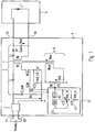
- the operating device 1 preferably has an input stage 2, a converter 3, a detection unit 4 and a control unit ST.
- the input stage 2 is optional and can be used to filter the mains supply voltage Vmains.
- the input stage 2 filter components or circuits (not shown).
- the input stage 2 can rectify the optionally filtered mains supply voltage Vmains, e.g. by a full-bridge rectifier with four diodes for converting the AC voltage into a pulsating DC voltage.
- the output of the optional input stage 2 is the voltage Vin and is supplied to the converter 3.
- This voltage Vin is preferably a rectified AC voltage, in particular a half-wave rectified AC voltage.
- the converter 3 is formed in the illustrated embodiment by a so-called flyback converter, which can also be referred to as flyback converter or high-buck converter.
- the converter 3 is a voltage converter or DC-DC converter and may also have alternative topologies, in particular topologies comprising a galvanic isolation.
- the flyback converter is in the embodiment of Fig. 1 that is, as an example of a clocked by at least one switch M1 electrically isolated converter, which may have a transformer for potential separation.
- the operating device 1 instead other clocked circuits, in particular with galvanic Have separation, such as a forward converter, also called forward converter, or a push-pull converter, also called push-pull converter, such as a push-pull converter with half-bridge or full bridge drive.
- the flyback converter 3 has a transformer T in the form of, for example, a transformer with a primary winding N1 and a secondary winding N2.
- the transformer T is used for potential separation between a primary side and a secondary side.
- the transformer T serves to transmit electrical energy from the primary winding N1 to the secondary winding N2 or from the primary side to the secondary side.
- the energy is preferably taken up in two different phases on the primary side and discharged again on the secondary side.
- a transformer in the form of a transformer therefore preferably has an air gap for temporarily storing the energy between the two phases.
- the flyback converter 3 comprises a controllable switch M1.
- a controllable switch M1 In a known manner can be transmitted to the secondary side of the flyback converter 3 by a corresponding alternately opening and closing the switch M1, the voltage applied from the input side to the flyback converter voltage Vin available. This transferred to the secondary side energy can be used to operate the secondary side connectable LED module 5. The energy transfer takes place in the open state of the switch M1, wherein for this purpose on the output side of the flyback converter 3, a diode D1 is further provided.
- the switch M1 is connected in series with the primary winding N1, so that by closing the controllable switch M1, a primary-side current can flow through this primary winding N1. When switch S1 is open, however, no current can flow through this primary winding N1.
- the switch M1 is designed, for example, as a controllable transistor, in particular as a FET or MOSFET transistor.
- the switch M1 is controlled by the control unit ST of the operating device.
- this control unit ST is located on the primary side of the flyback converter or the transformer T.
- the switch M1 is a MOSFET transistor, wherein the gate input of the switch M1 is designed as a control input and is connected to the control unit ST.
- the switch M1 is turned on and off via the control input by a control signal S / M1 generated by the control unit ST.
- the switch M1 of Fig. 1 is designed in particular as a p-channel, wherein the drain terminal is connected to a terminal of the primary winding N1.
- the source terminal of the switch M1 is preferably coupled to ground, ie to the primary side ground.
- the flyback converter 3 On the input side, the flyback converter 3 has a capacitor C_bulk, to which the input voltage Vin of the flyback converter 3 is applied.
- the diode D1 provided on the secondary side is connected in series with the secondary winding N2. Parallel to the series connection of the diode D1 and the secondary winding N2, a capacitor Cout is provided. The voltage across this capacitor Cout forms the output voltage Vout of the flyback converter 3, which in turn connects to two Output terminals K3, K4 is provided.
- the LED module 5 can be connected to these output terminals K3, K4.
- the LED module 5 has one or more LEDs, preferably an LED track comprising a plurality of LEDs connected in series.
- the LED module 5 may also comprise a parallel circuit of a plurality of LED paths or a mixed circuit of parallel and serially connected LEDs.
- a measuring resistor R1 can be provided between the switch M1 and ground. At this measuring resistor R1, a signal can be tapped, this signal VR1 the current 11 through the primary winding M1 reproduces. This measured signal is compared by a comparator Kp with a reference signal or with a reference voltage Vref_hi0. The output of the comparator Kp is fed to the control unit ST, as an alternative to the embodiment of the Fig. 1 the comparator Kp and the reference voltage Vref_hi0 may also be provided internally in the control unit ST.
- a maximum value I1max is provided for the primary-side current I1.
- This maximum value I1max can be externally supplied to the operating device 1, or can be determined by the operating device.
- the reference voltage Vref_hi0 is now preferably set so that when the primary-side current I1 reaches this maximum value I1max, then the measured signal VR1 corresponds to the reference Vref_hi0.
- the output of the comparator Kp thus provides the operating device 1 with information as to whether the primary-side current I1 is below the maximum value I1max or whether the primary-side current I1 has reached the maximum value I1max.
- the operating device 1 is thus able to switch M1 open as soon as the primary-side current I1 reaches the maximum value I1max or as soon as the measured signal VR1 reaches or exceeds the reference Vref_hi0.
- the typical time profile of the voltage VR1 representative of the current I1 is in Fig. 2 shown.
- the controllable switch M1 is controlled by the control unit ST of the operating device, preferably without electrical isolation between the switch M1 and the control unit ST.
- the transformer or the transformer T comprises in addition to the primary winding N1 and the secondary winding N2 nor an auxiliary winding or detection winding Naux, which is preferably located on the primary side of the transformer T.
- auxiliary winding Naux On the auxiliary winding Naux is a voltage Vaux, which reproduces the output voltage Vout.
- Vaux K1 * Vout, where K1 is a constant that depends on the winding ratios of the secondary winding and the auxiliary winding.
- an ohmic voltage divider consisting of two resistors R2, R3 is provided, at which a detection signal or a detection voltage VR3 for detecting the voltage Vaux at the auxiliary winding Naux is tapped.
- This tension VR3 is also representative of the output voltage Vout and proportional to the latter.
- the detection signal VR3 is supplied to the control unit ST.
- the detection winding Naux and the voltage divider R2, R3 together form the detection unit 4.
- the switch M1 When the switch M1 is switched on on the primary side, the current I1 rises constantly on the primary side, which induces a constant negative voltage Vaux in the detection unit 4. When the current I1 has reached the predetermined maximum value I1max, the power switch M1 is turned off. Thereafter, the detection voltage Vaux jumps to a positive value, oscillates for a certain period of time and then settles to a voltage value corresponding to the output voltage Vout.
- the detection voltage VR3 is preferably supplied to a first comparator K1 and a second comparator K2.
- the detection signal VR3 is compared with a first reference voltage Vref_lo.
- This reference voltage Vref_lo is preferably a switch-on threshold for switching on or switching back on the controllable switch M1.
- the switch M1 is turned on again on the primary side.
- this threshold Vref_lo is reached at time t4.
- the control signal S / M1 for switching on the switch M1 is then preferably increased, for example, from zero to a positive value.
- the switch M1 can be closed by the control unit ST as soon as the voltage at the auxiliary winding Naux reaches a corresponding lower threshold value. Since the detection voltage VR3 is representative of both the voltage Vaux on the auxiliary winding and the output voltage Vout, therefore, the switch M1 is closed again as soon as the output voltage Vout has reached a corresponding lower threshold value.
- the reference voltage Vref_lo is preferably a fixed comparator threshold, which can be preset, for example.
- the reference voltage Vref_lo can for example be predefined in the operating device 1, or it can be preset externally via a corresponding interface of the operating device 1. After the specification of a certain value Vref_lo, this reference voltage preferably remains constant. At least the reference Vref_lo remains constant for the duration of several switching cycles of the switch M1. In particular, the reference Vref_lo is independent of feedback values or measured values from the range of the operating device 1 or the LED module 5.
- the reference voltage Vref_lo is preferably less than half, in particular less than 20%, 10% or 5% of the detection voltage VR3 in the steady state after opening the switch M1.
- the flyback converter 3 can be operated according to a continuous current mode (current continuous conduction mode), a discontinuous current mode (discontinuous current mode), or according to an operation in the boundary region between continuous and discontinuous current current operation.
- the operating device 1 according to the invention is operated in this boundary region, which is also called critical conduction mode or borderline mode.
- critical conduction mode the switch M1 of the flyback converter 3 is turned on as soon as it is detected that the current through the secondary winding N2 has dropped to zero.
- the switch M1 is turned on when the detection voltage VR3 reaches or falls below the lower reference voltage Vref_lo.
- the current I2 through the secondary winding N2 is a measure of the current through the LEDs or through the LED module 5.
- the mean value of the current I2 corresponds to the mean value of the current through the LEDs.
- the second comparator K2 is now used in particular for accurately detecting the discharge time Tdischarge the secondary winding N2 between turning off the switch M1 and reaching the zero point by the secondary side current I2, wherein at the zero crossing of the current I2, the voltage Vaux on the auxiliary winding Naux or the detection voltage VR3 kinks.
- the second comparator K2 compares the detection voltage VR3 with a variable reference voltage in the form of an adaptive threshold Vref_hi.
- the sense voltage is also applied to a sample-and-hold circuit S + H, the latter being able to briefly hold the analog values of the sense voltage.
- This sample-and-hold circuit S + H is used in particular to sample the steady-state when the switch is turned off.
- the output of the sample-and-hold circuit is fed to an analog-to-digital converter ADC for converting the analog values into digital values.
- the adaptive threshold value Vref_hi is preferably dependent on the value of the output voltage Vout in the steady state state determined by the sample-and-hold circuit S + H and the analog-to-digital converter ADC. This dependence is in Fig. 1 represented by the arrow 8.
- an adaptive restart threshold Vref_hi is selected.
- the adaptive switch-on threshold Vref_hi may be selected as a certain percentage below the steady-state voltage, eg, 95%, 90%, or 80% of the value of the steady-state voltage VR3.
- This reference voltage Vref_lo is in particular smaller than the adaptive threshold value Vref_hi.
- the reference voltage Vref_lo is also preferably a non-variable value. Turning the switch M1 back on depending on the first comparator K1 is advantageous in that e.g. when the low reference voltage Vref_lo is reached, the mains voltage Vmains is also low, so that the losses in the switch M1 can be kept low.
- the undershooting of the adaptive, and thus higher selected, reclosing threshold Vref_hi is thus preferably taken only for more accurate determination of the discharge period Tdischarge for the indirect determination of the secondary-side current I2.
- the actual reconnection of the primary-side switch preferably takes place only when, in the further course of the decay of the detection voltage VR3, the threshold value Vref_lo, which is still fixed, is undershot.
- Fig. 2 shows the course of different sizes of the operating device 1 over a period Tperiod of the flyback converter 3, ie during the period of a complete switching cycle of the switch consisting of a switch-on time Ton of the switch M1 and a subsequent turn-off time Toff of the switch M1.
- Tperiod of the flyback converter 3 ie during the period of a complete switching cycle of the switch consisting of a switch-on time Ton of the switch M1 and a subsequent turn-off time Toff of the switch M1.
- Tperiod of the flyback converter 3 ie during the period of a complete switching cycle of the switch consisting of a switch-on time Ton of the switch M1 and a subsequent turn-off time Toff of the switch M1.
- the control unit ST generates the control signal S / M1 for driving the switch M1.
- the switch M1 is closed by the control unit ST by means of the control signal S / M1.
- the control signal S / M1 causes the opening of the switch M1 during a turn-off period toff.
- the switch M1 is alternately turned on and off, so that in operation after the in Fig. 2 turn off time toff again a turn-on time ton occurs.
- the switch-on time duration t on and the following switch-off time duration t off together form a period Tperiod of the operating device 1 or of the flyback converter 3. In operation, this results in a sequence of several periods Tperiod.
- the primary-side current I1 through the primary winding N1 and through the switch M1 is reproduced from the measuring voltage VR1, this measurement being picked up at the measuring resistor R1.
- a current flows through the primary winding N1.
- This primary-side current I1 rises linearly from a zero value.
- the measured signal VR1 also increases during the on-time period ton as in Fig. 2 shown.
- the control unit ST causes the switch M1 to be opened. Consequently, the diode D1 is operated in the forward direction and in the transformer energy stored during the turn-on period ton is transmitted to the secondary side of the transformer T. At time t1, therefore, the secondary-side current I2 through the diode D1 increases to a positive value and begins to decrease linearly again.
- Fig. 2 also shows the course of the voltage Vaux and the auxiliary winding Naux and the measured voltage VR3, these voltages are proportional to each other.
- the detected voltage has a constant negative value.
- the detection voltage jumps to a positive value, oscillates for a certain period of time and then settles to a voltage value corresponding to the output voltage Vout.
- the steady-state oscillation voltage after oscillation can remain constant or have a constant negative slope.
- this steady-state detection voltage has a kinking.
- this kinking occurs when the current I2 drops to zero through the secondary winding N2.
- the detection voltage Vaux oscillates the detection voltage Vaux, in which it preferably alternately drops to zero and rises again.
- the threshold value Vref_hi for detecting the discharge period Tdischarge is preferably dependent on the value of the settled detection voltage VR3.
- a waiting time WT can be stored in the control unit ST.
- This waiting time WT is in Fig. 2 represents and defines the period of time after Switching off the switch M1 must be awaited before the detection voltage VR3 is detected or sampled to determine the threshold value Vref_hi.
- the waiting time WT which must be met after switching off the switch to be sure that the output voltage or the detection voltage VR3 has settled, can be fixed as already seen.
- this waiting time WT can be fixed only at the beginning of the LED operation.
- this wait time WT can be adaptively redefined.
- the waiting time of a particular cycle may be a certain percentage of the discharge duration Tdischarge of the previous cycle.
- Fig. 2 shows, for example, that at the beginning of the LED operation, the output voltage or the detection voltage VR3 is detected after the predetermined waiting time WT.
- a waiting time WT ' is waited, this waiting time WT' being, for example, x% of the unloading time Tdischarge, eg 90% or 80%.
- correction factor .DELTA.T which depends on the sampled reference voltage VR3 is then determined as a correction factor.
- These correction values .DELTA.T can be empirical values, for example, which can be stored in a memory or in a look-up table within the control unit ST. The correspondence between the sampled reference voltage VR3 and the consequent correction value ⁇ T is stored in this memory or in this look-up table.
- the common denominator of these embodiments is therefore that the discharge period Tdischarge is preferably determined taking into account the detection of the detection voltage or the output voltage in the steady state.
- the comparator can be eliminated.
- the kinking of the detection voltage VR3 at the time t3 after the stationary state can be detected directly with a fast analog-to-digital converter.
- Comparator K2 is not needed and replaced by an analog-to-digital converter (not shown).
- the control unit ST checks the digital data generated by this analog-to-digital converter. As soon as the detection voltage VR3 is in the steady state, the control unit ST detects a possible bending of the detection voltage VR3 on the basis of this digital data. The detected time of the kinking is then determined by the control unit ST as the zero crossing of the current I2. Based on the time duration between the switching off of the switch M1 and the bending of the detection voltage, the control unit ST can finally determine the secondary current, as explained above.
- the output voltage Vout is detected indirectly, namely as the voltage which is stationary at the auxiliary winding Naux in the switched off switch state.
- a more direct detection of the output voltage can also be provided, in particular via the detection of a secondary-side parameter, for example via the detection of the output voltage Vout, and then transmission via the galvanic isolation, for example by means of optocouplers.
- the common denominator of the invention is therefore that the output voltage Vout is detected directly or indirectly, on the primary side or on the secondary side, and is included in the calculation of the discharge period Tdischarge as a variable.
Landscapes
- Engineering & Computer Science (AREA)
- Power Engineering (AREA)
- Dc-Dc Converters (AREA)
- Circuit Arrangement For Electric Light Sources In General (AREA)
- Led Devices (AREA)
Description
Die Erfindung betrifft ein Betriebsgerät zur Ansteuerung von Leuchtmitteln wie z.B. LED-Strecken, sowie eine Steuereinheit zur Ansteuerung eines solchen Betriebsgeräts. Zusätzlich betrifft die Erfindung auch ein Verfahren zur Ansteuerung von Leuchtmitteln wie z.B. LED-Strecken.The invention relates to an operating device for controlling lighting means such. LED routes, as well as a control unit for controlling such a control gear. In addition, the invention also relates to a method for controlling lighting means, such as e.g. LED routes.
Bekannt ist die Verwendung eines Flyback-Konverters zum Betrieb eines LED-Moduls. Der Flyback-Konverter ist Teil eines entsprechenden Betriebsgeräts und wird z.B. im Critical Conduction Modus, auch Borderline Modus genannt, betrieben. Dabei wird der Schalter des Flyback-Konverters primärseitig eingeschaltet, sodass in dieser Einschalt-Phase der primärseitige Strom konstant ansteigt. Dies verursacht bei einer Erfassungswicklung am Flyback-Konverter eine konstante negative Spannung.It is known to use a flyback converter to operate an LED module. The flyback converter is part of a corresponding operating device and is used e.g. operated in Critical Conduction mode, also called Borderline mode. In this case, the switch of the flyback converter is switched on the primary side, so that in this switch-on phase, the primary-side current increases constantly. This causes a constant negative voltage on a detection winding on the flyback converter.
Wenn der Strom einen vorgegebenen Peak-Wert erreicht hat, wird der Schalter abgeschaltet. Nach dem Abschalten springt die Spannung an der Erfassungswicklung auf einen positiven Wert, oszilliert während einer gewissen Zeitdauer und pendelt sich dann auf einen Spannungswert ein, der der Ausgangsspannung Vout entspricht.When the current has reached a predetermined peak value, the switch is turned off. After switching off, the voltage on the detection winding jumps to a positive value, oscillates for a certain period of time and then settles to a voltage value corresponding to the output voltage Vout.
Der sekundärseitige Strom nimmt während dieser Abschalt-Phase linear ab. Wenn der sekundärseitige Strom den Nullpunkt erreicht, sinkt die eingeschwungene und vorzugsweise lineare Spannung an der Erfassungswicklung. Beim Nullpunkt des sekundärseitigen Stroms knickt die Spannung an der Erfassungswicklung somit ab. Im Critical Conduction Modus ist es nunmehr erforderlich, den Nullpunkt des sekundärseitigen Stroms erfassen zu können, um dann den Schalter des Flyback-Konverters wieder einzuschalten.The secondary side current decreases linearly during this shutdown phase. When the secondary side current reaches zero, the steady and preferably linear voltage on the detection winding decreases. At the zero point of the secondary-side current, the voltage at the detection winding thus buckles. In Critical Conduction mode it is now necessary to use the To be able to detect zero point of the secondary-side current, and then turn on the switch of the flyback converter again.
Druckschrift
Das Problem bei der Technik gemäß dem Stand der Technik ist nunmehr, dass die eigentliche Zeitdauer bis zum Nulldurchgang des sekundärseitigen Strom, nicht genau erfasst werden kann, wenn eine solche feste Komparatorschwelle gewählt ist.
Die Erfindung setzt nunmehr daran an, dass eine adaptive Wiedereinschaltschwelle als Detektionsschwelle gewählt wird. Insbesondere kann diese Wiedereinschaltschwelle genauer das Abknicken der Erfassungsspannung erfassen, indem die bei ausgeschaltenem Schalter eingeschwungene Spannung abgetastet wird und abhängig davon, d.h. als Funktion der abgetasteten Spannung die Abschaltschwelle gewählt wird. Die eingeschwungene Spannung, die also der Ausgangsspannung des Flyback-Konverters entspricht, hängt von der konkreten Ausgestaltung des LED-Moduls ab, insbesondere von der Anzahl der LEDs in dem LED-Modul.pamphlet
The problem with the prior art technique now is that the actual time to zero crossing of the secondary current can not be accurately detected when such a fixed comparator threshold is selected.
The invention is now based on the fact that an adaptive switch-on threshold is selected as the detection threshold. In particular, this switch-on threshold can more accurately detect the kinking of the detection voltage by sampling the steady-state voltage when the switch is switched off, and depending on this, ie, the switch-off threshold is selected as a function of the sampled voltage. The steady-state voltage, which thus corresponds to the output voltage of the flyback converter, depends on the specific configuration of the LED module, in particular on the number of LEDs in the LED module.
Gemäß der Erfindung ist ein Betriebsgerät nach Anspruch 1 vorgesehen. Vorteilhafte Ausführungsformen des erfindungsgemäßen Betriebsgerätes sind durch die abhängigen Ansprüche definiert.According to the invention, an operating device according to
Gemäß dem Aspekt der Erfindung ist auch ein Verfahren nach Anspruch 8 vorgesehen. Eine vorteilhafte Ausführungsform des erfindungsgemäßen Verfahrens ist durch die abhängige Anspruch definiert.According to the aspect of the invention, a method according to
Die Beschreibung der Erfindung erfolgt nun auch mit Bezug auf die beigefügten Zeichnungen. Dabei zeigen:
-
Fig. 1 schematisch das Schaltbild eines Ausführungsbeispiels eines erfindungsgemäßen Betriebsgeräts für Leuchtmittel, -
Fig. 2 den Verlauf von elektrischen Größen des erfindungsgemäßen Betriebsgeräts, und -
Fig. 3 den Verlauf von elektrischen Größen des erfindungsgemäßen Betriebsgeräts gemäß einer alternativen Ausführungsform.
Das in
Das
-
Fig. 1 1 is a schematic diagram of an exemplary embodiment of a control device according to the invention for lighting devices; -
Fig. 2 the course of electrical variables of the operating device according to the invention, and -
Fig. 3 the course of electrical variables of the operating device according to the invention according to an alternative embodiment.
This in
The operating
Das Betriebsgerät 1 weist vorzugsweise eine Eingangsstufe 2, einen Konverter 3, eine Erfassungseinheit 4 und eine Steuereinheit ST auf. Die Eingangsstufe 2 ist optional und kann zum Filtern der Netzversorgungsspannung Vmains dienen. Hierzu kann die Eingangsstufe 2 Filter-Bauteile bzw. -Schaltungen (nicht gezeigt) aufweisen. Zusätzlich oder alternativ dazu kann die Eingangsstufe 2 eine Gleichrichtung der gegebenenfalls gefilterten Netzversorgungsspannung Vmains durchführen, z.B. durch einen Vollbrückengleichrichter mit vier Dioden zur Umwandlung der Wechselspannung in eine pulsierende Gleichspannung. Der Ausgang der gegebenenfalls vorhandenen Eingangsstufe 2 ist die Spannung Vin und wird dem Konverter 3 zugeführt. Diese Spannung Vin ist vorzugsweise eine gleichgerichtete Wechselspannung, insbesondere eine einweggleichgerichtete Wechselspannung.The operating
Der Konverter 3 ist im dargestellten Ausführungsbeispiel durch einen sogenannten Flyback-Konverter gebildet, der auch als Sperrwandler oder Hoch-Tiefsetzsteller bezeichnet werden kann. Im Allgemeinen ist der Konverter 3 ein Spannungswandler bzw. Gleichspannungswandler und kann auch alternative Topologien aufweisen, insbesondere Topologien aufweisend eine galvanische Trennung. Der Flyback-Konverter ist im Ausführungsbeispiel der
Der Flyback-Konverter 3 weist einen Übertrager T in Form beispielsweise eines Transformators mit einer Primärwicklung N1 und einer Sekundärwicklung N2 auf. Der Übertrager T dient zur Potentialtrennung zwischen einer Primärseite und einer Sekundärseite. Der Übertrager T dient zur Übertragung von elektrischer Energie von der Primärwicklung N1 zur Sekundärwicklung N2 bzw. von der Primärseite zu der Sekundärseite. Vorzugsweise wird die Energie in zwei unterschiedliche Phasen jeweils primärseitig aufgenommen und sekundärseitig wieder abgegeben. Ein Übertrager in Form eines Transformators weist deswegen zur Zwischenspeicherung der Energie zwischen den zwei Phasen vorzugsweise einen Luftspalt auf.The
Der Flyback-Konverter 3 umfasst einen steuerbaren Schalter M1. In bekannter Weise kann durch ein entsprechendes abwechselndes Öffnen und Schließen des Schalters M1 die von der eingangsseitig am Flyback-Konverter anliegenden Spannung Vin zur Verfügung gestellte Energie auf die Sekundärseite des Flyback-Konverters 3 übertragen werden. Diese auf die Sekundärseite übertragene Energie kann zum Betreiben des sekundärseitig anschließbaren LED-Moduls 5 verwendet werden. Die Energieübertragung findet dabei im geöffneten Zustand des Schalters M1 statt, wobei hierzu auf der Ausgangsseite des Flyback-Konverters 3 ferner eine Diode D1 vorgesehen ist.The
Der Schalter M1 ist in Serie zu der Primärwicklung N1 geschaltet, so dass durch Schließen des steuerbaren Schalters M1 ein primärseitiger Strom durch diese Primärwicklung N1 fließen kann. Bei geöffnetem Schalter S1 kann hingegen kein Strom durch diese Primärwicklung N1 fließen. Der Schalter M1 ist beispielsweise als steuerbarer Transistor ausgestaltet, insbesondere als FET oder MOSFET-Transistor. Der Schalter M1 wird von der Steuereinheit ST des Betriebsgeräts gesteuert. Vorzugsweise befindet sich diese Steuereinheit ST auf der Primärseite des Flyback-Konverters bzw. des Transformators T.The switch M1 is connected in series with the primary winding N1, so that by closing the controllable switch M1, a primary-side current can flow through this primary winding N1. When switch S1 is open, however, no current can flow through this primary winding N1. The switch M1 is designed, for example, as a controllable transistor, in particular as a FET or MOSFET transistor. The switch M1 is controlled by the control unit ST of the operating device. Preferably, this control unit ST is located on the primary side of the flyback converter or the transformer T.
Im dargestellten Ausführungsbeispiel ist der Schalter M1 ein MOSFET-Transistor, wobei der Gate-Eingang des Schalters M1 als Steuereingang ausgestaltet ist und mit der Steuereinheit ST verbunden ist. Der Schalter M1 wird über den Steuereingang von einem Steuersignal S/M1, das von der Steuereinheit ST erzeugt wird, ein- und ausgeschaltet. Der Schalter M1 der
Eingangsseitig weist der Flyback-Konverter 3 einen Kondensator C_bulk auf, an welchem die Eingangsspannung Vin des Flyback-Konverters 3 anliegt. Die auf der Sekundärseite vorgesehene Diode D1 ist in Serie mit der Sekundärwicklung N2 geschaltet. Parallel zu der Reihenschaltung der Diode D1 und der Sekundärwicklung N2 ist ein Kondensator Cout vorgesehen. Die Spannung an diesem Kondensator Cout bildet die Ausgangsspannung Vout des Flyback-Konverters 3, die wiederum an zwei Ausgangsklemmen K3, K4 zur Verfügung gestellt wird. An diese Ausgangsklemmen K3, K4 kann das LED-Modul 5 angeschlossen werden. Das LED-Modul 5 weist eine oder mehrere LEDs, vorzugsweise eine LED-Strecke aufweisend mehrere in Serie geschaltete LEDs, auf. Das LED-Modul 5 kann auch eine Parallel-Schaltung von mehreren LED-Strecken oder eine gemischte Schaltung aus parallel und seriell geschalteten LEDs aufweisen.On the input side, the
Vorzugsweise kann zwischen dem Schalter M1 und Masse ein Messwiderstand R1 vorgesehen sein. An diesem Messwiderstand R1 kann ein Signal abgegriffen werden, wobei dieses Signal VR1 den Strom 11 durch die Primärwicklung M1 wiedergibt. Dieses gemessene Signal wird von einem Komparator Kp mit einem Referenzsignal bzw. mit einer Referenzspannung Vref_hi0 verglichen. Der Ausgang des Komparators Kp wird der Steuereinheit ST zugeführt, wobei alternativ zum Ausführungsbeispiel der
Vorzugsweise ist ein Maximalwert I1max für den primärseitigen Strom I1 vorgesehen. Dieser Maximalwert I1max kann extern dem Betriebsgerät 1 zugeführt werden, oder kann vom Betriebsgerät festgelegt werden. Die Referenzspannung Vref_hi0 ist nun vorzugsweise so eingestellt, dass wenn der primärseitige Strom I1 diesen Maximalwert I1max erreicht, dann das gemessene Signal VR1 der Referenz Vref_hi0 entspricht. Der Ausgang des Komparators Kp liefert dem Betriebsgerät 1 somit eine Information, ob der primärseitige Strom I1 sich unterhalb des Maximalwerts I1max befindet, oder ob der primärseitige Strom I1 den Maximalwert I1max erreicht hat. Das Betriebsgerät 1 ist somit in der Lage, den Schalter M1 zu öffnen, sobald der primärseitige Strom I1 den Maximalwert I1max bzw. sobald das gemessene Signal VR1 die Referenz Vref_hi0 erreicht bzw. überschreitet. Der typische zeitliche Verlauf der für den Strom I1 repräsentativen Spannung VR1 ist in
Die Ansteuerung des steuerbaren Schalters M1 erfolgt durch die Steuereinheit ST des Betriebsgeräts, vorzugsweise ohne galvanische Trennung zwischen dem Schalter M1 und der Steuereinheit ST. Die Steuereinheit ST steuert hierbei den Schalter M1 alternierend an, wobei sich das Tastverhältnis TV bzw. der sogenannte Duty-Cycle für den Schaltbetrieb des Schalters M1 wie folgt berechnen lässt:
TV = ton / (Tperiod), wobei Tperiod die Gesamtdauer eines vollständigen Schaltzyklus für den Schalter M1 bezeichnet und ton der Einschaltzeitdauer des Schalters M1 entspricht.The controllable switch M1 is controlled by the control unit ST of the operating device, preferably without electrical isolation between the switch M1 and the control unit ST. The control unit ST controls the switch M1 alternately, wherein the duty cycle TV or the so-called duty cycle for the switching operation of the switch M1 can be calculated as follows:
TV = ton / (Tperiod), where Tperiod denotes the total duration of a complete switching cycle for the switch M1 and ton corresponds to the switch-on period of the switch M1.
Der Transformator bzw. der Übertrager T umfasst neben der Primärwicklung N1 und der Sekundärwicklung N2 noch eine Hilfswicklung oder Erfassungswicklung Naux, die sich vorzugsweise auf der Primärseite des Transformators T befindet. An der Hilfswicklung Naux liegt eine Spannung Vaux an, welche die Ausgangsspannung Vout wiedergibt. Insbesondere gilt Vaux = K1 * Vout, wobei K1 eine Konstante ist, die von den Wicklungsverhältnissen der Sekundärwicklung und der Hilfswicklung abhängt.The transformer or the transformer T comprises in addition to the primary winding N1 and the secondary winding N2 nor an auxiliary winding or detection winding Naux, which is preferably located on the primary side of the transformer T. On the auxiliary winding Naux is a voltage Vaux, which reproduces the output voltage Vout. In particular, Vaux = K1 * Vout, where K1 is a constant that depends on the winding ratios of the secondary winding and the auxiliary winding.
Parallel zu der Erfassungswicklung Naux ist ein ohmscher Spannungsteiler bestehend aus zwei Widerständen R2, R3 vorgesehen, an dem ein Erfassungssignal bzw. eine Erfassungsspannung VR3 zur Erfassung der Spannung Vaux an der Hilfswicklung Naux abgegriffen wird. Diese Spannung VR3 ist auch repräsentativ für die Ausgangsspannung Vout und proportional zu Letzterer. Das Erfassungssignal VR3 wird der Steuereinheit ST zugeführt. Die Erfassungswicklung Naux und der Spannungsteiler R2, R3 bilden zusammen die Erfassungseinheit 4.Parallel to the detection winding Naux, an ohmic voltage divider consisting of two resistors R2, R3 is provided, at which a detection signal or a detection voltage VR3 for detecting the voltage Vaux at the auxiliary winding Naux is tapped. This tension VR3 is also representative of the output voltage Vout and proportional to the latter. The detection signal VR3 is supplied to the control unit ST. The detection winding Naux and the voltage divider R2, R3 together form the detection unit 4.
Wenn der Schalter M1 primärseitig eingeschaltet ist, steigt der Strom I1 primärseitig konstant an, was bei der Erfassungseinheit 4 eine konstante negative Spannung Vaux induziert. Wenn der Strom I1 den vorgegebenen Maximalwert I1max erreicht hat, wird der Stromschalter M1 abgeschaltet. Daraufhin springt die Erfassungsspannung Vaux auf einen positiven Wert, oszilliert während einer gewissen Zeitdauer und pendelt sich dann auf einen Spannungswert ein, der der Ausgangsspannung Vout entspricht.When the switch M1 is switched on on the primary side, the current I1 rises constantly on the primary side, which induces a constant negative voltage Vaux in the detection unit 4. When the current I1 has reached the predetermined maximum value I1max, the power switch M1 is turned off. Thereafter, the detection voltage Vaux jumps to a positive value, oscillates for a certain period of time and then settles to a voltage value corresponding to the output voltage Vout.
Die Erfassungsspannung VR3 wird vorzugsweise einem ersten Komparator K1 und einem zweiten Komparator K2 zugeführt.The detection voltage VR3 is preferably supplied to a first comparator K1 and a second comparator K2.
Mit Hilfe des ersten Komparators K1 wird das Erfassungssignal VR3 mit einer ersten Referenzspannung Vref_lo verglichen. Diese Referenzspannung Vref_lo ist vorzugsweise eine Wiedereinschaltschwelle zum Einschalten bzw. Wiedereinschalten des steuerbaren Schalters M1. Wenn das Erfassungssignal VR3 diesen Schwellenwert Vref_lo erreicht bzw. unterschreitet, wird der Schalter M1 primärseitig wieder eingeschaltet. In
Somit kann der Schalter M1 von der Steuereinheit ST geschlossen werden, sobald die Spannung an der Hilfswicklung Naux einen entsprechenden unteren Schwellenwert erreicht. Da die Erfassungsspannung VR3 sowohl für die Spannung Vaux an der Hilfswicklung und für die Ausgangsspannung Vout repräsentativ ist, wird also der Schalter M1 wieder geschlossen, sobald die Ausgangsspannung Vout einen entsprechenden unteren Schwellenwert erreicht hat.Thus, the switch M1 can be closed by the control unit ST as soon as the voltage at the auxiliary winding Naux reaches a corresponding lower threshold value. Since the detection voltage VR3 is representative of both the voltage Vaux on the auxiliary winding and the output voltage Vout, therefore, the switch M1 is closed again as soon as the output voltage Vout has reached a corresponding lower threshold value.
Die Referenzspannung Vref_lo ist vorzugsweise eine feste Komparatorschwelle, die beispielsweise vorgegeben werden kann. Die Referenzspannung Vref_lo kann z.B. im Betriebsgerät 1 fest vordefiniert sein, oder sie kann extern über eine entsprechende Schnittstelle des Betriebsgeräts 1 vorgegeben werden. Nach der Vorgabe eines bestimmten Wertes Vref_lo bleibt diese Referenzspannung vorzugsweise konstant. Zumindest bleibt die Referenz Vref_lo für die Zeitdauer von mehreren Schaltzyklen des Schalters M1 konstant. Insbesondere ist die Referenz Vref_lo unabhängig von Rückführwerten oder Messwerten aus dem Bereich des Betriebsgeräts 1 oder des LED-Moduls 5. Die Referenzspannung Vref_lo ist vorzugsweise kleiner als die Hälfte, insbesondere kleiner als 20%, 10% oder 5% der Erfassungsspannung VR3 im eingeschwungenen Zustand nach Öffnen des Schalters M1.The reference voltage Vref_lo is preferably a fixed comparator threshold, which can be preset, for example. The reference voltage Vref_lo can for example be predefined in the
Der Flyback-Konverter 3 kann bekanntlich gemäß einem kontinuierlichen Strombetrieb (current continuous conduction mode), einem diskontinuierlichen Strombetrieb (current discontinuous conduction mode), oder gemäß einem Betrieb im Grenzbereich zwischen kontinuierlichem und diskontinuierlichem Strom Strombetrieb betrieben werden. Vorzugsweise wird das erfindungsgemäße Betriebsgerät 1 in diesem Grenzbereich, der auch Critical Conduction Modus oder Borderline Modus genannt wird, betrieben. Im Critical Conduction Modus wird der Schalter M1 des Flyback-Konverters 3 eingeschaltet, sobald erkannt wird, dass der Strom durch die Sekundärwicklung N2 auf Null abgesunken ist. Vorzugsweise wird der Schalter M1 eingeschaltet, wenn die Erfassungsspannung VR3 die untere Referenzspannung Vref_lo erreicht bzw. unterschreitet.The
Der Strom I2 durch die Sekundärwicklung N2 ist ein Maß für den Strom durch die LEDs bzw. durch das LED-Modul 5. Der Mittelwert des Stroms I2 entspricht dem Mittelwert des Stroms durch die LEDs. Zur Ausführung einer genauen Regelung des Stroms durch die LEDs ist es wichtig, die Zeitdauer Tdischarge zwischen dem Ausschalten des Schalters M1 und dem Absinken des Stroms I2 auf Null möglichst genau zu erfassen. Der Mittelwert des Stroms durch die Sekundärwicklung N2 kann nämlich wie folgt definiert werden:
I2 = I2max * 1/2 * Tdischarge / Tperiod, wobei I2max der Maximalwert des Stroms I2 unmittelbar nach dem Ausschalten des Schalters darstellt und Tperiod die Gesamtdauer eines vollständigen Schaltzyklus für den Schalter M1. In
I2 = I2max * 1/2 * Tdischarge / Tperiod, where I2max represents the maximum value of current I2 immediately after the switch is turned off and Tperiod represents the total duration of a complete switching cycle for switch M1. In
Der zweite Komparator K2 dient nunmehr insbesondere zur genauen Erfassung der Entlade-Zeitdauer Tdischarge der Sekundärwicklung N2 zwischen dem Abschalten des Schalters M1 und dem Erreichen des Nullpunkts durch den sekundärseitigen Stroms I2, wobei beim Nulldurchgang des Stroms I2 die Spannung Vaux an der Hilfswicklung Naux bzw. die Erfassungsspannung VR3 abknickt. Der zweite Komparator K2 vergleicht die Erfassungsspannung VR3 mit einer veränderbaren Referenzspannung in Form eines adaptiven Schwellenwerts Vref_hi.The second comparator K2 is now used in particular for accurately detecting the discharge time Tdischarge the secondary winding N2 between turning off the switch M1 and reaching the zero point by the secondary side current I2, wherein at the zero crossing of the current I2, the voltage Vaux on the auxiliary winding Naux or the detection voltage VR3 kinks. The second comparator K2 compares the detection voltage VR3 with a variable reference voltage in the form of an adaptive threshold Vref_hi.
Die Erfassungsspannung wird auch einer Sample-and-Hold-Schaltung S+H zugeführt, wobei Letztere die analogen Werte der Erfassungsspannung kurzzeitig halten kann. Diese Sample-and-Hold-Schaltung S+H wird insbesondere eingesetzt, um die bei ausgeschaltenem Schalter eingeschwungene Ausgangsspannung abzutasten. Der Ausgang der Sample-and-Hold-Schaltung wird einem Analog-Digital-Umsetzer ADC zugeführt zur Umsetzung der analogen Werte in digitale Werte.The sense voltage is also applied to a sample-and-hold circuit S + H, the latter being able to briefly hold the analog values of the sense voltage. This sample-and-hold circuit S + H is used in particular to sample the steady-state when the switch is turned off. The output of the sample-and-hold circuit is fed to an analog-to-digital converter ADC for converting the analog values into digital values.
Vorzugsweise ist der adaptive Schwellenwert Vref_hi abhängig von dem durch die Sample-and-Hold-Schaltung S+H und die den Analog-Digital-Umsetzer ADC ermittelten Wert der Ausgangsspannung Vout im eingeschwungenen Zustand. Diese Abhängigkeit wird in
Erfindungsgemäß wird also eine adaptive Wiedereinschaltschwelle Vref_hi gewählt. Beispielsweise kann die adaptive Wiedereinschaltschwelle Vref_hi als einem gewissen Prozentsatz unterhalb der eingeschwungenen Spannung gewählt werden, z.B. 95%, 90% oder 80% des Werts der eingeschwungenen Spannung VR3.According to the invention, therefore, an adaptive restart threshold Vref_hi is selected. For example, the adaptive switch-on threshold Vref_hi may be selected as a certain percentage below the steady-state voltage, eg, 95%, 90%, or 80% of the value of the steady-state voltage VR3.
Wie in
Diese Referenzspannung Vref_lo ist insbesondere kleiner als der adaptive Schwellenwert Vref_hi. Die Referenzspannung Vref_lo ist zudem vorzugsweise ein nicht veränderbarer Wert. Das Wiedereinschalten des Schalters M1 abhängig vom ersten Komparator K1 ist insofern vorteilhaft, dass z.B. bei Erreichen der niedrigen Referenzspannung Vref_lo auch die Netzspannung Vmains niedrig ist, so dass die Verluste im Schalter M1 niedrig gehalten werden können.This reference voltage Vref_lo is in particular smaller than the adaptive threshold value Vref_hi. The reference voltage Vref_lo is also preferably a non-variable value. Turning the switch M1 back on depending on the first comparator K1 is advantageous in that e.g. when the low reference voltage Vref_lo is reached, the mains voltage Vmains is also low, so that the losses in the switch M1 can be kept low.
Das Unterschreiten der adaptiv, und somit höher gewählten Wiedereinschaltschwelle Vref_hi wird also vorzugsweise nur zur genaueren Bestimmung der Entlade-Zeitdauer Tdischarge für die indirekte Bestimmung des sekundärseitigen Stroms I2 genommen. Das tatsächliche Wiedereinschalten des primärseitigen Schalters erfolgt indessen vorzugsweise erst dann, wenn im weiteren Verlauf des Abfallens der Erfassungsspannung VR3 der weiterhin fix vorgegebene Schwellewert Vref_lo unterschritten wird.The undershooting of the adaptive, and thus higher selected, reclosing threshold Vref_hi is thus preferably taken only for more accurate determination of the discharge period Tdischarge for the indirect determination of the secondary-side current I2. The actual reconnection of the primary-side switch, however, preferably takes place only when, in the further course of the decay of the detection voltage VR3, the threshold value Vref_lo, which is still fixed, is undershot.
Bezug nehmend auf
Der primärseitige Strom I1 durch die Primärwicklung N1 und durch den Schalter M1 wird von der Messspannung VR1 wiedergegeben, wobei diese Messung am Messwiderstand R1 abgegriffen wird. Während der Einschaltzeitdauer ton, d.h. während das Steuersignal S/M1 einen hohen Pegel aufweist, fließt ein Strom durch die Primärwicklung N1. Dieser primärseitige Strom I1 steigt linear ausgehend von einem Nullwert an. Entsprechend steigt auch das gemessene Signal VR1 während der Einschaltzeitdauer ton, wie in
Sobald zum Zeitpunkt t1 das für den primärseitigen Strom I1 repräsentative Messsignal VR1 den Schwellenwert Vref_hi0 erreicht, veranlasst die Steuereinheit ST ein Öffnen des Schalters M1. Folglich wird die Diode D1 in Durchlassrichtung betrieben und die im Transformator während der Einschaltzeitdauer ton gespeicherte Energie wird auf die Sekundärseite des Transformators T übertragen. Zum Zeitpunkt t1 steigt somit der sekundärseitige Strom I2 durch die Diode D1 auf einen positiven Wert und beginnt linear wieder abzunehmen.As soon as the measurement signal VR1 representative of the primary-side current I1 reaches the threshold value Vref_hi0 at the instant t1, the control unit ST causes the switch M1 to be opened. Consequently, the diode D1 is operated in the forward direction and in the transformer energy stored during the turn-on period ton is transmitted to the secondary side of the transformer T. At time t1, therefore, the secondary-side current I2 through the diode D1 increases to a positive value and begins to decrease linearly again.
Nach dem stationären Zustand mit konstantem Wert oder mit konstanter Steigung weist diese eingeschwungene Erfassungsspannung ein Abknicken auf. Vorzugsweise erfolgt dieses Abknicken, wenn der Strom I2 durch die Sekundärwicklung N2 auf Null abesinkt. Nach dem Abknicken oszilliert die Erfassungsspannung Vaux, in dem sie abwechselnd vorzugsweise auf Null absinkt und wieder ansteigt.After the stationary state with a constant value or with a constant slope, this steady-state detection voltage has a kinking. Preferably, this kinking occurs when the current I2 drops to zero through the secondary winding N2. After the kinking oscillates the detection voltage Vaux, in which it preferably alternately drops to zero and rises again.
Der Schwellenwert Vref_hi zum Erfassen der Entlade-Zeitdauer Tdischarge ist vorzugsweise abhängig von dem Wert der eingeschwungenen Erfassungsspannung VR3. Hierzu kann z.B. in der Steuereinheit ST eine Wartezeit WT hinterlegt sein. Diese Wartezeit WT ist in
t2 = t1 + WT, wobei t1 der Zeitpunkt des Abschaltens des Schalters M1 definiert.The threshold value Vref_hi for detecting the discharge period Tdischarge is preferably dependent on the value of the settled detection voltage VR3. For this purpose, for example, a waiting time WT can be stored in the control unit ST. This waiting time WT is in
t2 = t1 + WT, where t1 defines the time the switch M1 is turned off.
Die Wartezeit WT, die nach dem Abschalten des Schalters eingehalten werden muss, um sicher zu sein, dass die Ausgangsspannung bzw. die Erfassungsspannung VR3 eingeschwungen ist, kann wie bereits gesehen fest vorgegeben sein.The waiting time WT, which must be met after switching off the switch to be sure that the output voltage or the detection voltage VR3 has settled, can be fixed as already seen.
Alternativ, kann diese Wartezeit WT nur zu Beginn des LED-Betriebs fest vorgegeben. Sobald mindestens ein Ein- und Ausschaltzyklus durchgeführt wurden, kann dann diese Warte zeit WT adaptiv neu festgelegt werden. Z.B. kann die Wartezeit eines bestimmten Zyklus einen bestimmten Prozentsatz der Entlade-Zeitdauer Tdischarge des vorigen Zyklus betragen.
Nach einer weiteren Ausführungsform der Erfindung ist es vorgesehen, dass wiederum abhängig von dem Sampling bzw. Abtasten der eingeschwungenen Spannung Vaux bei ausgeschaltenem Schalter adaptiv, nämlich abhängig von diesem Sampling, die Entlade-Zeitdauer Tdischarge für die indirekte Bestimmung des sekundärseitigen Stroms I2 dadurch zu bestimmen, dass das Unterschreiten der Referenzspannung Vref_lo erfasst wird, und dann ein von dem Sampling-Wert abhängige Korrektur-Zeitdauer ΔT abgezogen wird, sozusagen als adaptiver Korrekturfaktor.According to a further embodiment of the invention, it is provided that, in turn, depending on the sampling or sampling of the settled voltage Vaux with the switch turned off adaptively, namely depending on this sampling, the discharge time period Tdischarge for the indirect determination of the secondary side current I2 determining that the falling below the reference voltage Vref_lo is detected, and then subtracting a correction time period ΔT dependent on the sampling value, so to speak as an adaptive correction factor.
Diese Ausführungsform ist z.B. dargestellt in
Der Korrekturwert ΔT wird dem Zeitpunkt t4 abgezogen, um den Zeitpunkt t3 des Nullstroms erfindungsgemäß zu ermitteln: ![]()
![]()
Gemeinsamer Nenner dieser Ausführungsbeispiele ist also, dass die Entlade-Zeitdauer Tdischarge vorzugsweise unter Berücksichtigung der Erfassung der Erfassungsspannung bzw. der Ausgangsspannung im eingeschwungenen Zustand bestimmt wird.The common denominator of these embodiments is therefore that the discharge period Tdischarge is preferably determined taking into account the detection of the detection voltage or the output voltage in the steady state.
Gemäß einer weiteren Ausführungsform kann der Komparator in Wegfall gebracht werden. Dafür kann wird das Abknicken der Erfassungsspannung VR3 zum Zeitpunkt t3 nach dem stationären Zustand mit einem schnellen Analog-Digital-Umsetzer direkt erfasst werden. In dieser Ausführungsform wird dann vorzugsweise der in
In dem dargestellten Ausführungsbeispiel der
Wie gesagt, dies dient nur zur korrekten Berechnung der Entlade-Zeitdauer Tdischarge, um somit wiederum indirekt den ausgangsseitigen mittleren Strom zu berechnen. Diese Erfassung hat indessen vorzugsweise keinen Einfluss auf das tatsächliche Wiedereinschalten des primärseitigen Schalters.As I said, this is only for the correct calculation of the discharge period Tdischarge, thus again indirectly calculate the output side average current. However, this detection preferably has no influence on the actual reconnection of the primary-side switch.
Wichtig ist, dass vorzugsweise gemäß der Erfindung keine den Strom durch die LEDs direkt oder indirekt wiedergebende Größe von der Sekundärseite auf die Primärseite zurückgeführt wird. Nur bei Wegfall dieser Überbrückung der galvanischen Trennung für diese Messgröße macht die indirekte Bestimmung des LED Stroms unter Einbeziehung der Ausschaltzeitdauer Toff Sinn.It is important that preferably no current directly or indirectly reflecting the current through the LEDs size is returned from the secondary side to the primary side according to the invention. Only if this bridging of the galvanic isolation for this measured variable is removed does the indirect determination of the LED current, including the switch-off period Toff, make sense.
Claims (9)
- An operating device (1) for operating lighting means, having:- a potential-isolated clocked converter (3), having a transformer (T), which has a primary winding (N1) and a secondary winding (N2), and a controllable switch (M1) arranged on the primary side, wherein the converter (3) can be supplied with a supply voltage on the primary side and the lighting means can be supplied on the secondary side by means of an output voltage (Vout) of the converter (3),- means (4) for directly or indirectly sensing the output voltage (Vout), and- a control unit (ST) for controlling the switch (M1), wherein the secondary current (I2) through the secondary winding (N2) linearly drops, starting from a positive value (I2max), while the switch (M1) is switched off,wherein the control unit (ST) is designed to sense a discharge duration (Tdischarge) between a switch-off of the switch (M1) and a subsequent drop in the secondary current (I2) to zero in order to control the secondary current (I2),
characterized in that
the control unit (ST) is designed to determine the discharge duration (Tdischarge) depending on a comparison of a sensed output voltage with an adaptive threshold value (Vref_hi). - An operating device according to Claim 1,
wherein the discharge duration (Tdischarge) is determined taking into consideration the sensing of a steady output voltage (Vout) after the switch-off of the switch (M1). - An operating device according to Claim 1,
wherein the adaptive threshold value (Vref-hi) is dependent on a value of the steady output voltage (Vout) after the switch-off of the switch (M1). - An operating device according to Claim 3,
wherein the control unit (ST) is designed to select the threshold value (Vref_hi) as a certain percentage below the value of the steady output voltage (Vout) after the switch-off of the switch (M1). - An operating device according to Claim 1 or 2,
wherein in order to sense the discharge duration (Tdischarge) initially a point in time (t4) of the undershooting of a fixed threshold value (Vref_10) is determined by the sensed output voltage (Vout), and then this point in time (t4) is corrected by an adaptive time duration (ΔT). - An operating device according to Claim 5,
wherein the adaptive time duration (ΔT) is dependent on a sensed value of the steady output voltage (Vout) after the switch-off of the switch (M1). - An operating device (1) according to Claim 1, having:an analog to digital converter for converting the output voltage (Vout) sensed in analog form into digital values,wherein the control unit (ST) is designed to sense a discharge duration (Tdischarge) between a switch-off of the switch (M1) and a subsequent drop in the secondary current (I2) to zero depending on the digital values in order to control the secondary current (I2).
- A method for operating lighting means
using a potential-isolated clocked converter (3), having a transformer (T), which has a primary winding (N1) and a secondary winding (N2), and a controllable switch (M1) arranged on the primary side,
wherein the secondary current (I2) through the secondary winding (N2) linearly drops, starting from a positive value (I2max), while the switch (M1) is switched off,
wherein the converter (3) is supplied with a supply voltage on the primary side, and the lighting means are supplied on the secondary side by means of an output voltage (Vout) of the converter (3),
wherein a discharge duration (Tdischarge) is sensed between a switch-off of the switch (M1) and a subsequent drop in the secondary current (I2) to zero in order to control the secondary current (12), characterized in that
the discharge duration (Tdischarge) is determined depending on a comparison of a sensed output voltage (Vout) with an adaptive threshold value (Vref_hi). - A method according to Claim 8,
wherein the output voltage (Vout) is directly or indirectly sensed and is converted into digital values, and
wherein the discharge duration (Tdischarge) is sensed between a switch-off of the switch (M1) and a subsequent drop in the secondary current (12) to zero depending on the digital values in order to control the secondary current (I2).
Applications Claiming Priority (2)
| Application Number | Priority Date | Filing Date | Title |
|---|---|---|---|
| DE102014204127.9A DE102014204127A1 (en) | 2014-03-06 | 2014-03-06 | LED driver |
| PCT/EP2015/052381 WO2015132032A2 (en) | 2014-03-06 | 2015-02-05 | Led driver |
Publications (2)
| Publication Number | Publication Date |
|---|---|
| EP3114898A2 EP3114898A2 (en) | 2017-01-11 |
| EP3114898B1 true EP3114898B1 (en) | 2018-12-05 |
Family
ID=52446378
Family Applications (1)
| Application Number | Title | Priority Date | Filing Date |
|---|---|---|---|
| EP15702500.8A Active EP3114898B1 (en) | 2014-03-06 | 2015-02-05 | Led driver |
Country Status (5)
| Country | Link |
|---|---|
| US (1) | US10172195B2 (en) |
| EP (1) | EP3114898B1 (en) |
| CN (1) | CN106105394B (en) |
| DE (1) | DE102014204127A1 (en) |
| WO (1) | WO2015132032A2 (en) |
Families Citing this family (7)
| Publication number | Priority date | Publication date | Assignee | Title |
|---|---|---|---|---|
| DE102015210710A1 (en) * | 2015-06-11 | 2016-12-15 | Tridonic Gmbh & Co Kg | Clocked flyback converter circuit |
| DE102016222161A1 (en) * | 2016-11-11 | 2018-05-17 | Tridonic Gmbh & Co Kg | Flyback converter for operating one or more lamps, associated method and operating device |
| CN108880274A (en) * | 2017-05-15 | 2018-11-23 | 赤多尼科两合股份有限公司 | A kind of output current detection circuit of controlled resonant converter |
| TWI629917B (en) * | 2017-07-26 | 2018-07-11 | 大樑科技實業有限公司 | Lighting system |
| CN108599108B (en) * | 2018-04-30 | 2023-11-17 | 上海晶丰明源半导体股份有限公司 | Protection circuit, driving system, chip, circuit protection method and driving method |
| EP4054066A1 (en) * | 2021-03-02 | 2022-09-07 | Tridonic GmbH & Co. KG | Synchronous flyback converter |
| DE102021113015B4 (en) | 2021-05-19 | 2023-07-27 | Steinel Gmbh | Circuit arrangement for a flyback power pack for operating and for detecting a temperature of at least one LED |
Citations (2)
| Publication number | Priority date | Publication date | Assignee | Title |
|---|---|---|---|---|
| US20040052095A1 (en) * | 2001-11-29 | 2004-03-18 | Iwatt, Inc | Methods for digital regulation of power converters using primary-only feedback |
| EP2645819A1 (en) * | 2012-03-30 | 2013-10-02 | Samsung Electro-Mechanics Co., Ltd | Light emitting diode driving apparatus |
Family Cites Families (11)
| Publication number | Priority date | Publication date | Assignee | Title |
|---|---|---|---|---|
| DE19828038A1 (en) * | 1998-06-24 | 1999-12-30 | Philips Corp Intellectual Pty | Switching power supply |
| US7016204B2 (en) | 2004-08-12 | 2006-03-21 | System General Corp. | Close-loop PWM controller for primary-side controlled power converters |
| JP4373995B2 (en) * | 2005-06-24 | 2009-11-25 | フリボ モバイル パワー ゲーエムベーハー | Control circuit for controlling current and voltage in switch mode power supplies |
| EP2110938B1 (en) * | 2008-04-14 | 2018-08-29 | Power Systems Technologies GmbH | Control circuit on the primary side of an electronic power converter having a transformer without auxiliary winding with a regulation based on the secondary side current flow duration |
| US9173261B2 (en) | 2010-07-30 | 2015-10-27 | Wesley L. Mokry | Secondary-side alternating energy transfer control with inverted reference and LED-derived power supply |
| US8912781B2 (en) | 2010-07-30 | 2014-12-16 | Cirrus Logic, Inc. | Integrated circuit switching power supply controller with selectable buck mode operation |
| CN102340911B (en) | 2010-12-30 | 2013-08-07 | 矽力杰半导体技术(杭州)有限公司 | Control circuit and control method for light emitting diode (LED) driver |
| CN103636109B (en) | 2011-06-03 | 2016-08-17 | 塞瑞斯逻辑公司 | For operating method and apparatus and the electric power distribution system of switched power transducer |
| KR20140017305A (en) | 2012-07-31 | 2014-02-11 | 삼성전기주식회사 | Driving apparatus for light emitting diode |
| CN103066872B (en) * | 2013-01-17 | 2015-06-17 | 矽力杰半导体技术(杭州)有限公司 | Integration switch power supply controller and switch power supply using the same |
| AT14906U1 (en) * | 2013-11-28 | 2016-08-15 | Tridonic Gmbh & Co Kg | LED module |
-
2014
- 2014-03-06 DE DE102014204127.9A patent/DE102014204127A1/en not_active Withdrawn
-
2015
- 2015-02-05 CN CN201580011822.2A patent/CN106105394B/en active Active
- 2015-02-05 US US15/122,498 patent/US10172195B2/en active Active
- 2015-02-05 WO PCT/EP2015/052381 patent/WO2015132032A2/en active Application Filing
- 2015-02-05 EP EP15702500.8A patent/EP3114898B1/en active Active
Patent Citations (2)
| Publication number | Priority date | Publication date | Assignee | Title |
|---|---|---|---|---|
| US20040052095A1 (en) * | 2001-11-29 | 2004-03-18 | Iwatt, Inc | Methods for digital regulation of power converters using primary-only feedback |
| EP2645819A1 (en) * | 2012-03-30 | 2013-10-02 | Samsung Electro-Mechanics Co., Ltd | Light emitting diode driving apparatus |
Also Published As
| Publication number | Publication date |
|---|---|
| CN106105394B (en) | 2019-05-07 |
| US20170079098A1 (en) | 2017-03-16 |
| DE102014204127A1 (en) | 2015-09-10 |
| WO2015132032A3 (en) | 2016-01-07 |
| US10172195B2 (en) | 2019-01-01 |
| CN106105394A (en) | 2016-11-09 |
| EP3114898A2 (en) | 2017-01-11 |
| WO2015132032A2 (en) | 2015-09-11 |
Similar Documents
| Publication | Publication Date | Title |
|---|---|---|
| EP3114898B1 (en) | Led driver | |
| DE102015102715B4 (en) | Power conversion with delay compensation | |
| DE102012205312B4 (en) | Burst mode of a switching converter | |
| DE102014104269B4 (en) | Switching power supply, which contains a flyback converter with primary-side control | |
| DE102013111348B4 (en) | Method and circuit arrangement for determining a demagnetization zero-current time | |
| EP2837259B1 (en) | Method of operating a llc resonance converter for a light source, and corresponding converter and led power source | |
| EP2249458B1 (en) | Emergency lighting apparatus for driving a light source, especially an LED | |
| EP3078242B1 (en) | Driving circuit for lighting means in especially leds | |
| DE102015104561A1 (en) | SYSTEM AND METHOD FOR A CONTACTED POWER CONVERTER | |
| EP2837262B1 (en) | Method for operating an llc resonant converter for an illuminant, converter and led converter | |
| DE10309189B4 (en) | DC converter circuit | |
| EP3207628B1 (en) | Operating circuit for energizing a lamp, led converter, and method for operating an operating circuit | |
| DE102015101673A1 (en) | power converter | |
| DE102017106503B4 (en) | drive circuit | |
| WO2012139846A1 (en) | Converter device | |
| EP1701434A2 (en) | Control circuit for the switch in a switched-mode power supply | |
| EP2992736B1 (en) | Method for operating an led converter | |
| EP3942684B1 (en) | Synchronous flyback converter | |
| AT17184U1 (en) | Converter circuit for light sources with one measuring point for recording combined electrical parameters | |
| EP3439159B1 (en) | Reduction of light power fluctuations in a threshold control system of an actively clocked converter | |
| EP3815469B1 (en) | Synchronous flyback converter for operating a lighting device | |
| DE102018116972B3 (en) | Operating circuit and method for operating an electrical load | |
| EP3791692B1 (en) | Synchronous flyback converter circuit for operating an illuminant line | |
| AT14335U1 (en) | LED driver | |
| EP2989863B1 (en) | Operating circuit for leds, having voltage measurement |
Legal Events
| Date | Code | Title | Description |
|---|---|---|---|
| PUAI | Public reference made under article 153(3) epc to a published international application that has entered the european phase |
Free format text: ORIGINAL CODE: 0009012 |
|
| STAA | Information on the status of an ep patent application or granted ep patent |
Free format text: STATUS: REQUEST FOR EXAMINATION WAS MADE |
|
| 17P | Request for examination filed |
Effective date: 20160811 |
|
| AK | Designated contracting states |
Kind code of ref document: A2 Designated state(s): AL AT BE BG CH CY CZ DE DK EE ES FI FR GB GR HR HU IE IS IT LI LT LU LV MC MK MT NL NO PL PT RO RS SE SI SK SM TR |
|
| AX | Request for extension of the european patent |
Extension state: BA ME |
|
| DAX | Request for extension of the european patent (deleted) | ||
| STAA | Information on the status of an ep patent application or granted ep patent |
Free format text: STATUS: EXAMINATION IS IN PROGRESS |
|
| 17Q | First examination report despatched |
Effective date: 20170901 |
|
| REG | Reference to a national code |
Ref country code: DE Ref legal event code: R079 Ref document number: 502015007097 Country of ref document: DE Free format text: PREVIOUS MAIN CLASS: H05B0033080000 Ipc: H02M0003335000 |
|
| GRAP | Despatch of communication of intention to grant a patent |
Free format text: ORIGINAL CODE: EPIDOSNIGR1 |
|
| STAA | Information on the status of an ep patent application or granted ep patent |
Free format text: STATUS: GRANT OF PATENT IS INTENDED |
|
| RIC1 | Information provided on ipc code assigned before grant |
Ipc: H02M 3/335 20060101AFI20180827BHEP Ipc: H05B 33/08 20060101ALI20180827BHEP |
|
| INTG | Intention to grant announced |
Effective date: 20180917 |
|
| GRAS | Grant fee paid |
Free format text: ORIGINAL CODE: EPIDOSNIGR3 |
|
| GRAA | (expected) grant |
Free format text: ORIGINAL CODE: 0009210 |
|
| STAA | Information on the status of an ep patent application or granted ep patent |
Free format text: STATUS: THE PATENT HAS BEEN GRANTED |
|
| AK | Designated contracting states |
Kind code of ref document: B1 Designated state(s): AL AT BE BG CH CY CZ DE DK EE ES FI FR GB GR HR HU IE IS IT LI LT LU LV MC MK MT NL NO PL PT RO RS SE SI SK SM TR |
|
| REG | Reference to a national code |
Ref country code: GB Ref legal event code: FG4D Free format text: NOT ENGLISH |
|
| REG | Reference to a national code |
Ref country code: CH Ref legal event code: EP |
|
| REG | Reference to a national code |
Ref country code: AT Ref legal event code: REF Ref document number: 1074302 Country of ref document: AT Kind code of ref document: T Effective date: 20181215 |
|
| REG | Reference to a national code |
Ref country code: IE Ref legal event code: FG4D Free format text: LANGUAGE OF EP DOCUMENT: GERMAN |
|
| REG | Reference to a national code |
Ref country code: DE Ref legal event code: R096 Ref document number: 502015007097 Country of ref document: DE |
|
| REG | Reference to a national code |
Ref country code: NL Ref legal event code: MP Effective date: 20181205 |
|
| REG | Reference to a national code |
Ref country code: LT Ref legal event code: MG4D |
|
| PG25 | Lapsed in a contracting state [announced via postgrant information from national office to epo] |
Ref country code: FI Free format text: LAPSE BECAUSE OF FAILURE TO SUBMIT A TRANSLATION OF THE DESCRIPTION OR TO PAY THE FEE WITHIN THE PRESCRIBED TIME-LIMIT Effective date: 20181205 Ref country code: LV Free format text: LAPSE BECAUSE OF FAILURE TO SUBMIT A TRANSLATION OF THE DESCRIPTION OR TO PAY THE FEE WITHIN THE PRESCRIBED TIME-LIMIT Effective date: 20181205 Ref country code: HR Free format text: LAPSE BECAUSE OF FAILURE TO SUBMIT A TRANSLATION OF THE DESCRIPTION OR TO PAY THE FEE WITHIN THE PRESCRIBED TIME-LIMIT Effective date: 20181205 Ref country code: LT Free format text: LAPSE BECAUSE OF FAILURE TO SUBMIT A TRANSLATION OF THE DESCRIPTION OR TO PAY THE FEE WITHIN THE PRESCRIBED TIME-LIMIT Effective date: 20181205 Ref country code: BG Free format text: LAPSE BECAUSE OF FAILURE TO SUBMIT A TRANSLATION OF THE DESCRIPTION OR TO PAY THE FEE WITHIN THE PRESCRIBED TIME-LIMIT Effective date: 20190305 Ref country code: ES Free format text: LAPSE BECAUSE OF FAILURE TO SUBMIT A TRANSLATION OF THE DESCRIPTION OR TO PAY THE FEE WITHIN THE PRESCRIBED TIME-LIMIT Effective date: 20181205 Ref country code: NO Free format text: LAPSE BECAUSE OF FAILURE TO SUBMIT A TRANSLATION OF THE DESCRIPTION OR TO PAY THE FEE WITHIN THE PRESCRIBED TIME-LIMIT Effective date: 20190305 |
|
| PG25 | Lapsed in a contracting state [announced via postgrant information from national office to epo] |
Ref country code: GR Free format text: LAPSE BECAUSE OF FAILURE TO SUBMIT A TRANSLATION OF THE DESCRIPTION OR TO PAY THE FEE WITHIN THE PRESCRIBED TIME-LIMIT Effective date: 20190306 Ref country code: RS Free format text: LAPSE BECAUSE OF FAILURE TO SUBMIT A TRANSLATION OF THE DESCRIPTION OR TO PAY THE FEE WITHIN THE PRESCRIBED TIME-LIMIT Effective date: 20181205 Ref country code: SE Free format text: LAPSE BECAUSE OF FAILURE TO SUBMIT A TRANSLATION OF THE DESCRIPTION OR TO PAY THE FEE WITHIN THE PRESCRIBED TIME-LIMIT Effective date: 20181205 Ref country code: AL Free format text: LAPSE BECAUSE OF FAILURE TO SUBMIT A TRANSLATION OF THE DESCRIPTION OR TO PAY THE FEE WITHIN THE PRESCRIBED TIME-LIMIT Effective date: 20181205 |
|
| PG25 | Lapsed in a contracting state [announced via postgrant information from national office to epo] |
Ref country code: NL Free format text: LAPSE BECAUSE OF FAILURE TO SUBMIT A TRANSLATION OF THE DESCRIPTION OR TO PAY THE FEE WITHIN THE PRESCRIBED TIME-LIMIT Effective date: 20181205 |
|
| PG25 | Lapsed in a contracting state [announced via postgrant information from national office to epo] |
Ref country code: IT Free format text: LAPSE BECAUSE OF FAILURE TO SUBMIT A TRANSLATION OF THE DESCRIPTION OR TO PAY THE FEE WITHIN THE PRESCRIBED TIME-LIMIT Effective date: 20181205 Ref country code: CZ Free format text: LAPSE BECAUSE OF FAILURE TO SUBMIT A TRANSLATION OF THE DESCRIPTION OR TO PAY THE FEE WITHIN THE PRESCRIBED TIME-LIMIT Effective date: 20181205 Ref country code: PT Free format text: LAPSE BECAUSE OF FAILURE TO SUBMIT A TRANSLATION OF THE DESCRIPTION OR TO PAY THE FEE WITHIN THE PRESCRIBED TIME-LIMIT Effective date: 20190405 Ref country code: PL Free format text: LAPSE BECAUSE OF FAILURE TO SUBMIT A TRANSLATION OF THE DESCRIPTION OR TO PAY THE FEE WITHIN THE PRESCRIBED TIME-LIMIT Effective date: 20181205 |
|
| PG25 | Lapsed in a contracting state [announced via postgrant information from national office to epo] |
Ref country code: SM Free format text: LAPSE BECAUSE OF FAILURE TO SUBMIT A TRANSLATION OF THE DESCRIPTION OR TO PAY THE FEE WITHIN THE PRESCRIBED TIME-LIMIT Effective date: 20181205 Ref country code: EE Free format text: LAPSE BECAUSE OF FAILURE TO SUBMIT A TRANSLATION OF THE DESCRIPTION OR TO PAY THE FEE WITHIN THE PRESCRIBED TIME-LIMIT Effective date: 20181205 Ref country code: SK Free format text: LAPSE BECAUSE OF FAILURE TO SUBMIT A TRANSLATION OF THE DESCRIPTION OR TO PAY THE FEE WITHIN THE PRESCRIBED TIME-LIMIT Effective date: 20181205 Ref country code: RO Free format text: LAPSE BECAUSE OF FAILURE TO SUBMIT A TRANSLATION OF THE DESCRIPTION OR TO PAY THE FEE WITHIN THE PRESCRIBED TIME-LIMIT Effective date: 20181205 Ref country code: IS Free format text: LAPSE BECAUSE OF FAILURE TO SUBMIT A TRANSLATION OF THE DESCRIPTION OR TO PAY THE FEE WITHIN THE PRESCRIBED TIME-LIMIT Effective date: 20190405 |
|
| REG | Reference to a national code |
Ref country code: DE Ref legal event code: R097 Ref document number: 502015007097 Country of ref document: DE |
|
| REG | Reference to a national code |
Ref country code: CH Ref legal event code: PL |
|
| PLBE | No opposition filed within time limit |
Free format text: ORIGINAL CODE: 0009261 |
|
| STAA | Information on the status of an ep patent application or granted ep patent |
Free format text: STATUS: NO OPPOSITION FILED WITHIN TIME LIMIT |
|
| PG25 | Lapsed in a contracting state [announced via postgrant information from national office to epo] |
Ref country code: LU Free format text: LAPSE BECAUSE OF NON-PAYMENT OF DUE FEES Effective date: 20190205 Ref country code: SI Free format text: LAPSE BECAUSE OF FAILURE TO SUBMIT A TRANSLATION OF THE DESCRIPTION OR TO PAY THE FEE WITHIN THE PRESCRIBED TIME-LIMIT Effective date: 20181205 Ref country code: MC Free format text: LAPSE BECAUSE OF FAILURE TO SUBMIT A TRANSLATION OF THE DESCRIPTION OR TO PAY THE FEE WITHIN THE PRESCRIBED TIME-LIMIT Effective date: 20181205 Ref country code: DK Free format text: LAPSE BECAUSE OF FAILURE TO SUBMIT A TRANSLATION OF THE DESCRIPTION OR TO PAY THE FEE WITHIN THE PRESCRIBED TIME-LIMIT Effective date: 20181205 |
|
| 26N | No opposition filed |
Effective date: 20190906 |
|
| REG | Reference to a national code |
Ref country code: BE Ref legal event code: MM Effective date: 20190228 |
|
| REG | Reference to a national code |
Ref country code: IE Ref legal event code: MM4A |
|
| PG25 | Lapsed in a contracting state [announced via postgrant information from national office to epo] |
Ref country code: LI Free format text: LAPSE BECAUSE OF NON-PAYMENT OF DUE FEES Effective date: 20190228 Ref country code: CH Free format text: LAPSE BECAUSE OF NON-PAYMENT OF DUE FEES Effective date: 20190228 |
|
| PG25 | Lapsed in a contracting state [announced via postgrant information from national office to epo] |
Ref country code: IE Free format text: LAPSE BECAUSE OF NON-PAYMENT OF DUE FEES Effective date: 20190205 |
|
| PG25 | Lapsed in a contracting state [announced via postgrant information from national office to epo] |
Ref country code: BE Free format text: LAPSE BECAUSE OF NON-PAYMENT OF DUE FEES Effective date: 20190228 |
|
| PG25 | Lapsed in a contracting state [announced via postgrant information from national office to epo] |
Ref country code: TR Free format text: LAPSE BECAUSE OF FAILURE TO SUBMIT A TRANSLATION OF THE DESCRIPTION OR TO PAY THE FEE WITHIN THE PRESCRIBED TIME-LIMIT Effective date: 20181205 |
|
| PGFP | Annual fee paid to national office [announced via postgrant information from national office to epo] |
Ref country code: AT Payment date: 20200220 Year of fee payment: 6 |
|
| PG25 | Lapsed in a contracting state [announced via postgrant information from national office to epo] |
Ref country code: MT Free format text: LAPSE BECAUSE OF FAILURE TO SUBMIT A TRANSLATION OF THE DESCRIPTION OR TO PAY THE FEE WITHIN THE PRESCRIBED TIME-LIMIT Effective date: 20181205 |
|
| REG | Reference to a national code |
Ref country code: DE Ref legal event code: R084 Ref document number: 502015007097 Country of ref document: DE |
|
| PG25 | Lapsed in a contracting state [announced via postgrant information from national office to epo] |
Ref country code: CY Free format text: LAPSE BECAUSE OF FAILURE TO SUBMIT A TRANSLATION OF THE DESCRIPTION OR TO PAY THE FEE WITHIN THE PRESCRIBED TIME-LIMIT Effective date: 20181205 |
|
| PG25 | Lapsed in a contracting state [announced via postgrant information from national office to epo] |
Ref country code: HU Free format text: LAPSE BECAUSE OF FAILURE TO SUBMIT A TRANSLATION OF THE DESCRIPTION OR TO PAY THE FEE WITHIN THE PRESCRIBED TIME-LIMIT; INVALID AB INITIO Effective date: 20150205 |
|
| REG | Reference to a national code |
Ref country code: AT Ref legal event code: MM01 Ref document number: 1074302 Country of ref document: AT Kind code of ref document: T Effective date: 20210205 |
|
| PG25 | Lapsed in a contracting state [announced via postgrant information from national office to epo] |
Ref country code: AT Free format text: LAPSE BECAUSE OF NON-PAYMENT OF DUE FEES Effective date: 20210205 |
|
| PG25 | Lapsed in a contracting state [announced via postgrant information from national office to epo] |
Ref country code: MK Free format text: LAPSE BECAUSE OF FAILURE TO SUBMIT A TRANSLATION OF THE DESCRIPTION OR TO PAY THE FEE WITHIN THE PRESCRIBED TIME-LIMIT Effective date: 20181205 |
|
| P01 | Opt-out of the competence of the unified patent court (upc) registered |
Effective date: 20230530 |
|
| PGFP | Annual fee paid to national office [announced via postgrant information from national office to epo] |
Ref country code: DE Payment date: 20240228 Year of fee payment: 10 Ref country code: GB Payment date: 20240220 Year of fee payment: 10 |
|
| PGFP | Annual fee paid to national office [announced via postgrant information from national office to epo] |
Ref country code: FR Payment date: 20240226 Year of fee payment: 10 |