EP3113406B1 - Key protecting method and apparatus - Google Patents
Key protecting method and apparatus Download PDFInfo
- Publication number
- EP3113406B1 EP3113406B1 EP14884251.1A EP14884251A EP3113406B1 EP 3113406 B1 EP3113406 B1 EP 3113406B1 EP 14884251 A EP14884251 A EP 14884251A EP 3113406 B1 EP3113406 B1 EP 3113406B1
- Authority
- EP
- European Patent Office
- Prior art keywords
- core
- key
- executed
- module
- memory
- Prior art date
- Legal status (The legal status is an assumption and is not a legal conclusion. Google has not performed a legal analysis and makes no representation as to the accuracy of the status listed.)
- Active
Links
- 238000000034 method Methods 0.000 title claims description 100
- 230000008569 process Effects 0.000 claims description 56
- 230000007246 mechanism Effects 0.000 claims description 23
- 206010000210 abortion Diseases 0.000 claims description 6
- 238000010586 diagram Methods 0.000 description 5
- 230000001360 synchronised effect Effects 0.000 description 4
- 230000001133 acceleration Effects 0.000 description 3
- 238000006243 chemical reaction Methods 0.000 description 3
- 230000001010 compromised effect Effects 0.000 description 1
- 230000006870 function Effects 0.000 description 1
- 230000004048 modification Effects 0.000 description 1
- 238000012986 modification Methods 0.000 description 1
- 230000002093 peripheral effect Effects 0.000 description 1
Images


Classifications
-
- H—ELECTRICITY
- H04—ELECTRIC COMMUNICATION TECHNIQUE
- H04L—TRANSMISSION OF DIGITAL INFORMATION, e.g. TELEGRAPHIC COMMUNICATION
- H04L9/00—Cryptographic mechanisms or cryptographic arrangements for secret or secure communications; Network security protocols
- H04L9/08—Key distribution or management, e.g. generation, sharing or updating, of cryptographic keys or passwords
- H04L9/0816—Key establishment, i.e. cryptographic processes or cryptographic protocols whereby a shared secret becomes available to two or more parties, for subsequent use
- H04L9/0819—Key transport or distribution, i.e. key establishment techniques where one party creates or otherwise obtains a secret value, and securely transfers it to the other(s)
- H04L9/0822—Key transport or distribution, i.e. key establishment techniques where one party creates or otherwise obtains a secret value, and securely transfers it to the other(s) using key encryption key
-
- G—PHYSICS
- G06—COMPUTING; CALCULATING OR COUNTING
- G06F—ELECTRIC DIGITAL DATA PROCESSING
- G06F12/00—Accessing, addressing or allocating within memory systems or architectures
- G06F12/02—Addressing or allocation; Relocation
- G06F12/08—Addressing or allocation; Relocation in hierarchically structured memory systems, e.g. virtual memory systems
- G06F12/0802—Addressing of a memory level in which the access to the desired data or data block requires associative addressing means, e.g. caches
- G06F12/0806—Multiuser, multiprocessor or multiprocessing cache systems
-
- G—PHYSICS
- G06—COMPUTING; CALCULATING OR COUNTING
- G06F—ELECTRIC DIGITAL DATA PROCESSING
- G06F9/00—Arrangements for program control, e.g. control units
- G06F9/06—Arrangements for program control, e.g. control units using stored programs, i.e. using an internal store of processing equipment to receive or retain programs
- G06F9/46—Multiprogramming arrangements
- G06F9/466—Transaction processing
- G06F9/467—Transactional memory
-
- H—ELECTRICITY
- H04—ELECTRIC COMMUNICATION TECHNIQUE
- H04L—TRANSMISSION OF DIGITAL INFORMATION, e.g. TELEGRAPHIC COMMUNICATION
- H04L9/00—Cryptographic mechanisms or cryptographic arrangements for secret or secure communications; Network security protocols
- H04L9/002—Countermeasures against attacks on cryptographic mechanisms
-
- H—ELECTRICITY
- H04—ELECTRIC COMMUNICATION TECHNIQUE
- H04L—TRANSMISSION OF DIGITAL INFORMATION, e.g. TELEGRAPHIC COMMUNICATION
- H04L9/00—Cryptographic mechanisms or cryptographic arrangements for secret or secure communications; Network security protocols
- H04L9/08—Key distribution or management, e.g. generation, sharing or updating, of cryptographic keys or passwords
- H04L9/0894—Escrow, recovery or storing of secret information, e.g. secret key escrow or cryptographic key storage
-
- H—ELECTRICITY
- H04—ELECTRIC COMMUNICATION TECHNIQUE
- H04L—TRANSMISSION OF DIGITAL INFORMATION, e.g. TELEGRAPHIC COMMUNICATION
- H04L9/00—Cryptographic mechanisms or cryptographic arrangements for secret or secure communications; Network security protocols
- H04L9/14—Cryptographic mechanisms or cryptographic arrangements for secret or secure communications; Network security protocols using a plurality of keys or algorithms
-
- H—ELECTRICITY
- H04—ELECTRIC COMMUNICATION TECHNIQUE
- H04L—TRANSMISSION OF DIGITAL INFORMATION, e.g. TELEGRAPHIC COMMUNICATION
- H04L9/00—Cryptographic mechanisms or cryptographic arrangements for secret or secure communications; Network security protocols
- H04L9/30—Public key, i.e. encryption algorithm being computationally infeasible to invert or user's encryption keys not requiring secrecy
-
- H—ELECTRICITY
- H04—ELECTRIC COMMUNICATION TECHNIQUE
- H04L—TRANSMISSION OF DIGITAL INFORMATION, e.g. TELEGRAPHIC COMMUNICATION
- H04L9/00—Cryptographic mechanisms or cryptographic arrangements for secret or secure communications; Network security protocols
- H04L9/32—Cryptographic mechanisms or cryptographic arrangements for secret or secure communications; Network security protocols including means for verifying the identity or authority of a user of the system or for message authentication, e.g. authorization, entity authentication, data integrity or data verification, non-repudiation, key authentication or verification of credentials
- H04L9/3226—Cryptographic mechanisms or cryptographic arrangements for secret or secure communications; Network security protocols including means for verifying the identity or authority of a user of the system or for message authentication, e.g. authorization, entity authentication, data integrity or data verification, non-repudiation, key authentication or verification of credentials using a predetermined code, e.g. password, passphrase or PIN
-
- G—PHYSICS
- G06—COMPUTING; CALCULATING OR COUNTING
- G06F—ELECTRIC DIGITAL DATA PROCESSING
- G06F2212/00—Indexing scheme relating to accessing, addressing or allocation within memory systems or architectures
- G06F2212/10—Providing a specific technical effect
- G06F2212/1052—Security improvement
-
- G—PHYSICS
- G06—COMPUTING; CALCULATING OR COUNTING
- G06F—ELECTRIC DIGITAL DATA PROCESSING
- G06F2212/00—Indexing scheme relating to accessing, addressing or allocation within memory systems or architectures
- G06F2212/40—Specific encoding of data in memory or cache
- G06F2212/402—Encrypted data
-
- G—PHYSICS
- G06—COMPUTING; CALCULATING OR COUNTING
- G06F—ELECTRIC DIGITAL DATA PROCESSING
- G06F2212/00—Indexing scheme relating to accessing, addressing or allocation within memory systems or architectures
- G06F2212/60—Details of cache memory
-
- G—PHYSICS
- G06—COMPUTING; CALCULATING OR COUNTING
- G06F—ELECTRIC DIGITAL DATA PROCESSING
- G06F2212/00—Indexing scheme relating to accessing, addressing or allocation within memory systems or architectures
- G06F2212/62—Details of cache specific to multiprocessor cache arrangements
- G06F2212/621—Coherency control relating to peripheral accessing, e.g. from DMA or I/O device
Definitions
- the present disclosure relates to a computer security field, and more particularly to a key protecting method and apparatus.
- private data are protected with cryptography.
- keys are generated in pairs. Each pair of keys consist of a private key and a public key. The private key is kept only by the owner.
- the premise for protecting private data with a public-key cryptographic algorithm is ensuring confidentiality of the private key.
- the private key is stored and operated in a memory.
- system intrusions and physical attacks severely threaten the security of the computer system.
- the system intrusions utilize a software bug of the system and directly obtain the private key via memory access instructions.
- the physical attacks such as a cold boot attack, may obtain an image of the whole Random-Access Memory (RAM) chip while there is a physical access with a target computer.
- RAM Random-Access Memory
- a general practice is storing the key with resources in the CPU, rather than resources in the RAM.
- this scheme may only support a symmetric cryptographic algorithm and a simple asymmetric cryptographic algorithm, in which length of the key is limited.
- the other kind of scheme is applicable to a multi-core processor and stores the key and intermediate variables in an on-chip cache of the CPU. This kind of scheme utilizes a write back mode of the cache to clear up contents, which are newly written into the memory, before the contents are synchronized to the RAM chip and only computation results are reserved. Meanwhile, in order to eliminate influence of cache sharing, when the cryptographic computation is performed, all cores, which share the cache with the cryptographic computation core, need to be configured as a no-fill mode.
- embodiments of the present disclosure provide a key protection method and device to resist system intrusions and physical attacks on the memory to ensure security of the implementation of public-key cryptographic algorithm in the computer system and enhance efficiency of the processor.
- an embodiment of the present disclosure provides a key protection method, including:
- step B and step C when another core and the operation core of the multi-core processor try to access a same memory address and at least one write operation is executed, or when the cache is replaced due to insufficiency of space of the cache, all operations executed by the operation core are aborted and the step B and step C are re-executed.
- the method further includes:
- the method further includes: specifying codes corresponding to the step B and step C as a transactional region via a transactional memory mechanism, so that the multi-core processor dynamically records all the memory accesses in the process for executing the step B and step C, aborts all the operations executed by the operation core and re-executes the step B and step C when another core and the operation core of the multi-core processor try to access the same memory address and at least one write operation is executed or when the cache is replaced due to insufficiency of the space of the cache occupied by the operation core.
- the method further includes: specifying codes corresponding to the step B and step C as a transactional region via Intel Transactional Synchronization Extensions (TSX), so that the multi-core processor dynamically records all the memory access in the process for executing the step B and step C, aborts all the operations executed by the operation core and re-executes the step B and step C when another core and the operation core of the multi-core processor try to access the same memory address and at least one write operation is executed or when the cache is replaced due to insufficiency of the space of the cache occupied by the operation core.
- TSX Intel Transactional Synchronization Extensions
- the method further includes: aborting all the operations executed by the operation core and re-executing the step B and step C via a Restricted Transactional Memory (RTM) mechanism of the Intel TSX when another core and the operation core of the multi-core processor try to access the same memory address and at least one write operation is executed or when the cache is replaced due to insufficiency of the space of the cache occupied by the operation core.
- RTM Restricted Transactional Memory
- the method further includes: entering the transactional region via begin instructions (such as xbegin instruction) in a Restricted Transactional Memory (RTM) mechanism and specifying beginning of the step B as a feedback address when another core and the operation core of the multi-core processor try to access the same access memory address and at least one write operation is executed or specifying the beginning of the step B as the fallback address when the cache is replaced due to insufficiency of the cache occupied by the operation core, and existing the transactional region via end instructions (such as xend instruction) when execution of the step C is finished.
- begin instructions such as xbegin instruction
- RTM Restricted Transactional Memory
- the method for setting the symmetric master key in each core of the multi-core processor in the step A includes:
- the specified registers of the multi-core processor for storing the symmetric master key include a debug register and Performance Monitor Counter (PMC) register.
- PMC Performance Monitor Counter
- the public-key cryptographic operation includes: a plaintext private key obtaining operation and a private-key computation operation.
- the plaintext private key obtaining operation includes: reading, by the operation core, a private key encrypted with the symmetric master key from a hard disk, and copying the private key to a memory, decrypting, by the operation core, the private key encrypted by the symmetric master key in the specified register in the multi-core processor to obtain the plaintext private key and storing the plaintext private key in the cache occupied by the operation core;
- the private-key computation operation comprises: a digital signature and/or decryption step, wherein the digital signature and/or decryption operation is executed with the plaintext private key, the method further includes: storing the intermediate variables private-key computation and a computation result generated in the private-key computation operation in the cache occupied by the operation core.
- the plaintext private key obtaining operation decrypts the private key encrypted with the symmetric master key using a Streaming Single Instruction Multiple Data (SIMD) Extension (SSE) register via calling Advanced Encryption Standard-New Instruction (AES-NI) instructions and copies the plaintext private key to the cache.
- SIMD Streaming Single Instruction Multiple Data
- SSE Streaming Single Instruction Multiple Data
- AES-NI Advanced Encryption Standard-New Instruction
- the step C further includes: clearing up data in the SSE register and a general-purpose register.
- the method further includes: prohibiting OS process scheduling and disabling local interrupts.
- the method further includes: restoring the OS process scheduling and enabling the local interrupt.
- the OS process scheduling is prohibited and the local interrupts are disabled via clearing up an Interrupt Flag (IF) bit of the EFLAGS register of the multi-core processor and the OS process scheduling and local interrupt is enabled via setting the IF bit of the EFLAGS register of the multi-core processor.
- IF Interrupt Flag
- the method further includes: reserving a memory region accessed by the step B and step C for each core of the multi-core processor.
- Embodiments of the present disclosure further provide a key protection device for implementing the above methods.
- the key protection method provided by embodiments of the present disclosure may resist physical attacks and system intrusions. Via setting that each core of the multi-core processor may have one symmetric master key, dynamically obtaining the plaintext private key of the asymmetric algorithm via a decryption operation and using the Intel TSX, it may be ensured that the private key and the intermediate variables used in the computation process may be stored in the cache occupied by the operation core only in terms of the hardware level, which may prevent the attackers from stealing the private key from the physical memory and ensure the security of the implementation of public-key cryptographic algorithm in the computer system.
- the other cores of the multi-core processor may perform the cryptographic operation, which may enhance the operation efficiency.
- the present disclosure may be implemented based on following considerations: There may be various system level attacks on the memory. At present, the OS may provide some protection measures on sensitive memory space. However, if an attacker bypasses these protection measures with some bugs, the attacker may directly access the sensitive memory space and sensitive data may leak out.
- the present disclosure may dynamically monitor the sensitive data region via a hardware mechanism so that any direct access to the sensitive data region may be able to obtain a non-sensitive cipher text version only before sensitive data are written into the sensitive data region, which may greatly enhance the difficulty of the attacks on the memory system.
- the cold boot attack may attack a physical memory module.
- the on-chip cache is generally integrated into the Central Processing Unit (CPU), a key protection process for storing the plaintext private key and intermediate variables in the CPU on-chip cache proposed in the prior art is very effective.
- the cache In the structure of the computer memory hierarchy, the cache is a small-capacity storage at a high speed between the CPU and a main memory.
- the physical cores of the CPU and caches which are occupied by the physical cores of the CPU may constitute a relatively independent environment.
- the storage capacity of the cache is much larger than that of the register of the CPU, may be enough to store the keys of the public-key cryptographic algorithm and to provide various algorithms of security enhancement and arithmetic acceleration.
- Existing literatures may implement a 4096-bit Rivest-Shamir-Adleman (RSA) operation supporting a Chinese Remainder Theorem (CRT) with this method.
- RSA Rivest-Shamir-Adleman
- CRT Chinese Remain
- the number of cores, which may simultaneously perform the cryptographic operation may be influenced by the hierarchical structure of the cache.
- the existing CPU architecture may have a shared cache (such as L3 cache register), and this scheme may support only one core performing the cryptographic operation at the same time.
- the additional software protection mechanisms such as configuring other cores into the no-fill mode with software, which may affect the processing speed of the CPU since the other cores cannot simultaneously perform other cryptographic operation in the multi-core processor system.
- Another objective of the present disclosure may be preventing the cold boot attack via storing the plaintext private key and intermediate variables in the CPU on-chip cache and preventing slowdown of the processing speed of the CPU.
- Transactional memory is a technology put forwarded in the prior art for solving the problem of thread synchronization. Transactional memory may allow one thread to independently finish modification of the shared memory and may neglect that there may be other threads. However, the thread may record each read and write operation on shared memory in a log. If there may be concurrent operations on the shared memory, the thread may abort all the previous operations and fall back to the beginning state of the transaction.
- TSX Intel Transactional Synchronization Extensions
- Haswell architecture fourth-generation Core CPUs
- the programing interface of Intel TSX may be used to enhance utilization of existing CPU multi-core in multi-threading applications.
- the core of the Intel TSX technology is transactional memory.
- the procedure may take a code segment as a transactional region and all memory accesses made by the code segment may be recorded. If there is memory access conflict, abort may occur to abort all previous operations and the state of the CPU may be restored to that before entering the transactional region. Then, as for Restricted Transactional Memory (RTM), aborted operations may directly jump to a specified code area. Alternatively, as for Hardware Lock Elision (HLE), the above operations may be re-executed after locking. If there is no memory access conflict, all updates on the memory and registers may be atomically submitted. Therefore, before the update is finished, other cores may read old data only while accessing this segment of the memory.
- RTM Restricted Transactional Memory
- HLE Hardware Lock Elision
- the access conflict may refer to that an external thread may read a memory address, which may have been written before in the transactional region or an external thread may write a memory address, which may have been read or written before in the transactional region. If there is memory access conflict, transaction abort may occur.
- the basis for implementing transactional memory may be the cache-coherence protocol of the CPU. All memory accesses in the transactional region may occur in the cache of the operation core. If another core accesses a memory address recorded in the transactional region or the cache of the operation core should synchronize data in the cache to the memory due to insufficiency of space, the above operations may be detected by the cache-coherence protocol and aborts may occur based on the policy.
- the present disclosure may ensure that the sensitive data stored in the cache, such as the plaintext private key may not be synchronized to the memory with the transactional region of the above Intel TSX technology. Since the TSX may ensure the atomicity of the memory submission, the malware attacks of the system level may be prevented.
- An example of the present disclosure may provide a key protection method, which may be executed by a multi-core processor, as shown in figure 1 .
- a symmetric master key may be set in each core of a multi-core processor.
- any core of the multi-core processor may be taken as an operation core.
- the plaintext private key may be decrypted from the symmetric master key to execute a public-key cryptographic operation.
- Intermediate variables used in the public-key cryptographic operation and the plaintext private key may be stored in the cache occupied by the operation core.
- the plaintext private key and the intermediate variables used in the operation process in the cache occupied by the operation core may be cleared up.
- storing the plaintext private key and intermediate variables in the cache may prevent physical attacks, such as the cold boot attacks.
- the operation core may execute an abort operation. That is, the operation core may abort all previous operations and re-execute all operations, which may have been executed. Therefore, the other cores need not to be configured as the no-fill mode, so that multiple cores may simultaneously execute the cryptographic operation to improve the efficiency of the multi-core processor and prevent the system attacks.
- the multi-core processor may dynamically record all memory accesses in the execution process of the block B and block C.
- a determination as to whether other threads of the multi-core processor and the operation core simultaneously access a same memory address and at least one write operation is executed may be made according to all the memory accesses recorded.
- a determination as to whether the space of the cache is enough may be made according to the record of all the memory accesses.
- an embodiment of the present disclosure provides a key protection method, which may effectively resist physical attacks and system intrusions, shown in figure 2 and figure 3 .
- the method may include following blocks.
- each core of the multi-core processor may be configured to contain a symmetric master key (i.e., the symmetric master key may be set in each core of the multi-core processor).
- any core of the multi-core processor may be taken as an operation core.
- An decryption operation may be performed to obtain a plaintext private key using the symmetric master key.
- the public-key cryptographic operation may be performed using the plaintext private key.
- the plaintext private key and intermediate variables used in the operation process may be stored in the cache occupied by the operation core.
- the plaintext private key and the intermediate variables used in the operation process in the cache occupied by the operation core may be cleared up.
- the multi-core processor may dynamically record all memory accesses in the execution processes of the block B and block C.
- the operation core may abort all executed operations of the block B and block C (i.e., the operation core may abort all executed operations) and block B and block C may be re-executed until the block B and block C are finished.
- An operation may be performed to exit from the transactional region and submit the memory.
- the Intel Haswell processor performs the RSA public-key cryptographic operation
- the processor may be a four-core Intel Core i7 4770S.
- the used RSA algorithm may be implemented with Chinese Remainder Theorem (CRT) acceleration, Montgomery mode multiply acceleration and sliding window. Size of the sliding window may be 32 and the maximum memory used in the RSA computation may be 4708 bytes.
- Block A may be executed to make each core of the multi-core processor contain the symmetric master key.
- Block A may include following blocks.
- a prompt interface may pop up and a user may input a password.
- the OS may convert the password into the symmetric master key via a key generation algorithm.
- the symmetric master key may be copied to the specified registers of the multi-core processor, which may facilitate the public-key cryptographic operation.
- the specified registers may be debug registers or Performance Monitor Counter (PMC) registers.
- block B may be performed.
- Any core may be taken as the operation core to execute the public-key cryptographic operation.
- the plaintext private key and the intermediate variables in the operation process may be stored in the cache occupied by the operation core.
- the public-key cryptographic operation may include: a plaintext private key obtaining operation and a private-key computation operation.
- the operation core may read the private key encrypted with the symmetric master key from the hard disk and copy the private key to the memory.
- the operation core may decrypt the private key, which is encrypted with the symmetric master key with the symmetric master key stored in the specified registers of the multi-core process to obtain the plaintext private key and store the plaintext private key in the cache occupied by the operation core.
- the symmetric master key in the debug register or the PMC register may be written into the cache.
- the private key encrypted with the symmetric master key may be decrypted using the SSE register via calling Advanced Encryption Standard-New Instruction (AES-NI) instructions and the plaintext private key may be copied to the cache.
- AES-NI Advanced Encryption Standard-New Instruction
- the operation core may perform digital signature and/or decryption operation with the plaintext private key.
- intermediate variables generated in the computation process may be stored in the cache occupied by the operation core.
- the computation result may be stored in the cache occupied by a running core.
- block C may be executed.
- the plaintext private key and the intermediate variables used in the operation process in the cache occupied by the operation core may be cleared up and only the operation result may be kept.
- the multi-core processor may dynamically record all memory accesses in the execution process of the block B and block C.
- the operation core may abort all executed operations of the block B and block C and block B and block C may be re-executed.
- Codes corresponding to the block B and block C may be specified as the transactional region via transactional memory mechanism, such as Intel TSX mechanism.
- transactional memory mechanism such as Intel TSX mechanism.
- the multi-core processor may dynamically record all memory accesses of the codes in the transactional region. In other words, all memory accesses in the execution process of the block B and block C may be recorded.
- the operation core may abort all executed operations of the block B and block C and re-execute the block B and block C.
- the operation core may abort the operations and jump to a specified code region. Therefore, all memory write operations in the cryptographic operation process may occur in the cache only, which may prevent synchronization of the data from the cache to the memory and prevent the cold boot attacks. Further, when the other cores read the private key, re-execution may occur and the key information cannot be obtained.
- the present disclosure may not limit other processes in the multi-core processor to use the cache and may support that each core in the multi-core processor may use a different cryptographic operation to enhance efficiency of the multi-core processor.
- this example may further include prohibiting OS process scheduling and disabling local interrupts.
- the OS process scheduling and the local interrupts may be enabled.
- the OS process scheduling may be prohibited and the local interrupts may be disabled via clearing up an Interrupt Flag (IF) bit of the EFLAGS register of the multi-core processor and the OS process scheduling and the local interrupt may be enabled by setting the IF bit of the EFLAGS register of the multi-core processor.
- IF Interrupt Flag
- all memory accesses of the codes i.e., the codes corresponding to the plaintext private key obtaining operation and private-key computation operation
- all memory accesses of the codes i.e., the codes corresponding to the plaintext private key obtaining operation and private-key computation operation
- abort may occur.
- the operation core may abort the previous operations.
- the state of the operation core may be restored to that before entering into the transactional region.
- the operation core may jump to the specified code region (when the RTM is used).
- the operation core may use the SSE register and the general-purpose register in the operation process
- data in the SSE register and general-purpose register may also be cleared up.
- the data in the cache occupied by the operation core may be cleared up with the memset function and the data in the SSE register and general-purpose register may be cleared up with the XOR instruction.
- the present disclosure may preferably reserve a memory region accessed by the block B and block C for each core in the multi-core processor before executing the block B, i.e., before entering the transactional region. So that each core of the multi-core processor may access a fixed memory region via reserving the memory region, the conflict between the memory accesses of the other cores and the operation core transactional region may be avoided and the plaintext private key obtaining operation and private-key computation operation may be successfully carried out.
- the symmetric private key in plain text may be decrypted dynamically via making each core of the multi-core processor contain one symmetric master key. Further, in terms of the hardware, it may be ensured that the private key and the intermediate variables used in the computation process may be stored in the cache occupied by the core only via the Intel TSX. It may be prevented that the attacker may directly steal the private-key information from the physical memory or read the private-key information via malwares, so that the security of the implementation of public-key cryptographic algorithm in the computer system may be ensured. Further, the other cores of the multi-core processor may perform the cryptographic operations with the Intel TSX mechanism to improve the operation efficiency.
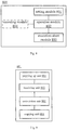
- FIG. 8 is a schematic diagram illustrating the structure of a key protection device in accordance with an example of the present disclosure.
- the key protection device 800 may include: a setting module 801, an operation module 802 and an execution-abort module 803.
- the setting module 801 may be to execute step A of setting a symmetric master key in each core of the multi-core processor.
- the operation module 802 may be to execute step B of taking any core of the multi-core processor as the operation core, performing a public-key cryptographic operation according to the symmetric master key set by the setting module 801.
- the plaintext private key and the intermediate variables used in the public-key cryptographic operation may be stored in the cache occupied by the operation core.
- the operation module 802 may further execute step C of clearing up the plaintext private key and the intermediate variables in the cache occupied by the operation core.
- the execution-abort module 803 may be to enable, in the process of executing the step B and step C, the operation module 802 to abort all executed operations and to re-execute the step B and step C when another core and the operation core of the multi-core processor try to access a same memory address and at least one write operation is executed, or when the cache is replaced due to insufficiency of space of the cache.
- the key protection device 800 may execute the steps in the method examples shown in figure 1 to figure 7 , which will not be described here in detail to avoid repetition.
- the multi-core processor 800 may further include a recording module 804.
- the recording module 804 may be to record all memory accesses dynamically in the process of executing the step B and step C when the operation module 802 executes the step B and step C.
- the operation module 802 may be further to determine whether another core and the operation core of the multi-core processor may simultaneously access the same memory address and at least one write operation may be executed according to all the memory accesses recorded by the recording module 804; or determine whether the space of the cache may be sufficient according to all the memory accesses recorded by the recording module 804.
- execution-abort module 803 may be to enable the operation module 802 to abort all the executed operations and to enable the operation module 802 to re-execute the step B and step C via transactional memory mechanism (such as the Intel TSX) when another thread and the operation core of the multi-core processor try to access the same memory address and at least one write operation is executed or when the cache is replaced due to insufficiency of the space of the cache.
- transactional memory mechanism such as the Intel TSX
- the execution-abort module 803 may be to enter a transactional region via begin instructions (such as xbegin instruction) in the Restricted Transactional Memory (RTM) mechanism of the Intel TSX and specify beginning of the step B executed by the operation module 802 as a fallback address when threads of other cores and the operation core of the multi-core processor try to access the same memory address and at least one write operation is executed or specify the beginning of the step B executed by the operation module 802 as the fallback address when the cache is replaced due to insufficiency of the space of the cache occupied by the operation core and exist the transactional region via end instructions (such as xend instruction) when execution of the step C is finished by the operation module 802.
- begin instructions such as xbegin instruction
- RTM Restricted Transactional Memory
- the operation core may abort the operations and jump to a specified code region. Therefore, all memory write operations in the cryptographic operation process may occur in the cache only, which may prevent synchronization of the data from the cache to the memory and prevent the cold boot attacks. Further, when the other cores read the private key, re-execution may occur and the key information cannot be obtained.
- the present disclosure does not limit the threads of other cores of the multi-core processor to use the cache and each core in the multi-core processor may use a different cryptographic operation to enhance efficiency of the multi-core processor.
- the setting module 801 may include: a popping up unit 901, a receiving unit 902, a conversion unit 903 and a copying unit 904.
- the popping up unit 901 may be to pop up a prompt interface when an OS boots.
- the receiving unit 902 may be to receive a password input by a user in the prompt interface popped up by the popping up unit 901.
- the conversion unit 903 may be to convert the password received by the receiving unit 902 into the symmetric master key via the OS adopting a key generation algorithm.
- the copying unit 904 may be to copy the symmetric master key converted by the conversion unit 903 to the specified registers in the multi-core processor for storage.
- the setting module 801 may be further to prohibit OS process scheduling and disable local interrupts before the operation module 802 executes the step B and enable the OS process scheduling and the local interrupts after the operation module 802 executes the step C. Therefore, the success rate of the public-key cryptographic operation may be improved.
- the setting module 801 may be further to prohibit the OS process scheduling and disable the local interrupts via clearing up the Interrupt Flag (IF) bit of the EFLAGS register of the multi-core processor and enable the OS process scheduling and local interrupts via setting the IF bit of the EFLAGS register of the multi-core processor.
- IF Interrupt Flag
- the setting module 801 may be further to reserve a memory region accessed when the operation module 802 executes the step B and step C for each core in the multi-core processor.
- each core of the multi-core process may access a fixed memory region, so that the conflict between the memory accesses of other cores and the transactional region of the operation core may be avoided and the plaintext private key obtaining operation and private-key computation operation may be successfully executed.
- This example may provide a device for executing the blocks in the above method.
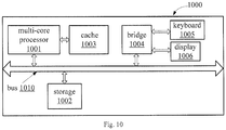
- FIG 10 is a schematic diagram illustrating a key protection device.
- the key protection device 1000 may include a multi-core processor 1001 and a storage 1002.
- the multi-core processor 1001 may further be called a Central Processing Unit (CPU).
- the storage 1002 may include: a Read-Only Memory (ROM) and a Random Access Memory (RAM) and provide the multi-core processor 1001 with instructions and data.
- the storage 1002 may include a Non-Volatile Random Access Memory (NVRAM).
- the processor 1001 may couple with the storage 1002 with a bus system 1010.
- the bus system 1010 may include: a power bus, a control bus and a state signal bus besides data bus. For clarity, various buses in the figure may be labeled as the bus system 1010.
- the methods in the above examples may be applied to the above key protection device 1000.
- the multi-core processor 1001 may be an integrated circuit chip with the signal processing ability.
- each block of the above methods may be implemented via an integrated logic circuit of the hardware or instructions in software format in the multi-core processor 1001.
- the multi-core processor 1001 may support Intel TSX and connect with a cache 1003. Sensitive information in the computation process may be stored in the device 1003.
- a user interface When the system boots, a user interface may be popped up and a password may need to be input into the user interface.
- These operations may be implemented via a keyboard 1005 and display 1006 connected with a bridge device 1004,
- the bridge device may be a high-speed Northbridge, which may be used to connect with a graphic display card or may be used to connect with a peripheral, such as a keyboard by a Southbridge.
Description
- The present disclosure relates to a computer security field, and more particularly to a key protecting method and apparatus.
- In a computer system, private data are protected with cryptography. In a public-key cryptographic algorithm, keys are generated in pairs. Each pair of keys consist of a private key and a public key. The private key is kept only by the owner. The premise for protecting private data with a public-key cryptographic algorithm is ensuring confidentiality of the private key.
- Normally, in the computer system, the private key is stored and operated in a memory. However, system intrusions and physical attacks severely threaten the security of the computer system. The system intrusions utilize a software bug of the system and directly obtain the private key via memory access instructions. The physical attacks, such as a cold boot attack, may obtain an image of the whole Random-Access Memory (RAM) chip while there is a physical access with a target computer. In order to prevent the cold boot attack, a general practice is storing the key with resources in the CPU, rather than resources in the RAM. These schemes may be classified into two categories. One kind of scheme is utilizing a register. Since the capacity of the register is limited, this scheme may only support a symmetric cryptographic algorithm and a simple asymmetric cryptographic algorithm, in which length of the key is limited. The other kind of scheme is applicable to a multi-core processor and stores the key and intermediate variables in an on-chip cache of the CPU. This kind of scheme utilizes a write back mode of the cache to clear up contents, which are newly written into the memory, before the contents are synchronized to the RAM chip and only computation results are reserved. Meanwhile, in order to eliminate influence of cache sharing, when the cryptographic computation is performed, all cores, which share the cache with the cryptographic computation core, need to be configured as a no-fill mode. In the no-fill mode, a memory access operation, which is a read miss or a write miss, does not incur replacement of the cache. It can be seen that in a situation that an L3 cache is shared by all cores of the multi-core processor, this kind of scheme supports only one core in performing the cryptographic operation at the same time. Further, when one core performs the cryptographic operation, other cores are configured as the no-fill mode, so that the processor is inefficient. Besides, as for this kind of configuration, if the Operating System (OS) has a bug, malicious processes still may directly read the keys stored in the memory via the bug, resulting in invalidity of the protection mechanism.
- D1 (
CN103607279A ) discloses a multi-core processor based key protection method and system. - D2 (
WO2014004222 ) discloses novel instructions, logic, methods and apparatus to test transactional execution status. - D3 (
US2014/040554 ) discloses an improved system and method for protecting large regions within a hardware transactional memory without operating system support. - As for the above problems in the prior art, embodiments of the present disclosure provide a key protection method and device to resist system intrusions and physical attacks on the memory to ensure security of the implementation of public-key cryptographic algorithm in the computer system and enhance efficiency of the processor.
- In order to achieve the above objectives, an embodiment of the present disclosure provides a key protection method, including:
- step A, setting a symmetric master key in each core of a multi-core processor;
- step B, taking any core of the multi-core processor configured to contain the symmetric master key as an operation core, performing a decryption operation to obtain a plaintext private key using the symmetric master key, performing a public-key cryptographic operation using the plaintext private key; the plaintext private key and intermediate variables used in the public-key cryptographic operation being stored in a cache occupied by the operation core; and
- step C, clearing up the plaintext private key and the intermediate variable used in the public-key cryptographic operation in the cache occupied by the operation core;
- in a process of executing the step B and step C, when another core and the operation core of the multi-core processor try to access a same memory address and at least one write operation is executed, or when the cache is replaced due to insufficiency of space of the cache, all operations executed by the operation core are aborted and the step B and step C are re-executed.
- The method further includes:
- recording all memory accesses dynamically in the process for executing the step B and step C when the step B and step C are executed;
- determining whether another core and the operation core of the multi-core processor simultaneously access the same memory address and at least one write operation is executed according to all the recorded memory accesses; or
- determining whether the space of the cache is sufficient according to all the recorded memory accesses.
- The method further includes:
specifying codes corresponding to the step B and step C as a transactional region via a transactional memory mechanism, so that the multi-core processor dynamically records all the memory accesses in the process for executing the step B and step C, aborts all the operations executed by the operation core and re-executes the step B and step C when another core and the operation core of the multi-core processor try to access the same memory address and at least one write operation is executed or when the cache is replaced due to insufficiency of the space of the cache occupied by the operation core. - The method further includes:
specifying codes corresponding to the step B and step C as a transactional region via Intel Transactional Synchronization Extensions (TSX), so that the multi-core processor dynamically records all the memory access in the process for executing the step B and step C, aborts all the operations executed by the operation core and re-executes the step B and step C when another core and the operation core of the multi-core processor try to access the same memory address and at least one write operation is executed or when the cache is replaced due to insufficiency of the space of the cache occupied by the operation core. - The method further includes:
aborting all the operations executed by the operation core and re-executing the step B and step C via a Restricted Transactional Memory (RTM) mechanism of the Intel TSX when another core and the operation core of the multi-core processor try to access the same memory address and at least one write operation is executed or when the cache is replaced due to insufficiency of the space of the cache occupied by the operation core. - The method further includes:
entering the transactional region via begin instructions (such as xbegin instruction) in a Restricted Transactional Memory (RTM) mechanism and specifying beginning of the step B as a feedback address when another core and the operation core of the multi-core processor try to access the same access memory address and at least one write operation is executed or specifying the beginning of the step B as the fallback address when the cache is replaced due to insufficiency of the cache occupied by the operation core, and existing the transactional region via end instructions (such as xend instruction) when execution of the step C is finished. - The method for setting the symmetric master key in each core of the multi-core processor in the step A includes:
- popping up, by an Operating System (OS), a prompt interface and receiving a password input by a user in the prompt interface;
- converting, by the OS, the password into the symmetric master key adopting a key generation algorithm; and
- copying the symmetric master key to specified registers in each core of the multi-core processor for storage.
- Further, the specified registers of the multi-core processor for storing the symmetric master key include a debug register and Performance Monitor Counter (PMC) register.
- The public-key cryptographic operation includes: a plaintext private key obtaining operation and a private-key computation operation.
- The plaintext private key obtaining operation includes: reading, by the operation core, a private key encrypted with the symmetric master key from a hard disk, and copying the private key to a memory, decrypting, by the operation core, the private key encrypted by the symmetric master key in the specified register in the multi-core processor to obtain the plaintext private key and storing the plaintext private key in the cache occupied by the operation core;
the private-key computation operation comprises: a digital signature and/or decryption step, wherein the digital signature and/or decryption operation is executed with the plaintext private key, the method further includes: storing the intermediate variables private-key computation and a computation result generated in the private-key computation operation in the cache occupied by the operation core. - The plaintext private key obtaining operation decrypts the private key encrypted with the symmetric master key using a Streaming Single Instruction Multiple Data (SIMD) Extension (SSE) register via calling Advanced Encryption Standard-New Instruction (AES-NI) instructions and copies the plaintext private key to the cache.
- The step C further includes: clearing up data in the SSE register and a general-purpose register.
- Before the step B, the method further includes: prohibiting OS process scheduling and disabling local interrupts.
- After the step C, the method further includes: restoring the OS process scheduling and enabling the local interrupt.
- Further, the OS process scheduling is prohibited and the local interrupts are disabled via clearing up an Interrupt Flag (IF) bit of the EFLAGS register of the multi-core processor and the OS process scheduling and local interrupt is enabled via setting the IF bit of the EFLAGS register of the multi-core processor.
- Before the step B is executed, the method further includes: reserving a memory region accessed by the step B and step C for each core of the multi-core processor.
- Embodiments of the present disclosure further provide a key protection device for implementing the above methods.
- The key protection method provided by embodiments of the present disclosure may resist physical attacks and system intrusions. Via setting that each core of the multi-core processor may have one symmetric master key, dynamically obtaining the plaintext private key of the asymmetric algorithm via a decryption operation and using the Intel TSX, it may be ensured that the private key and the intermediate variables used in the computation process may be stored in the cache occupied by the operation core only in terms of the hardware level, which may prevent the attackers from stealing the private key from the physical memory and ensure the security of the implementation of public-key cryptographic algorithm in the computer system. Further, even the OS is compromised and the attacker may directly read the memory space storing the key, since the Intel TSX mechanism may ensure the atomicity of the submission of the memory, the attacker cannot obtain the plaintext private key. Further, in this scheme, the other cores of the multi-core processor may perform the cryptographic operation, which may enhance the operation efficiency.
-
-
Figure 1 is a flow chart illustrating a key protection method in accordance with an example of the present disclosure; -
Figure 2 is a flow chart illustrating another key protection method in accordance with an example of the present disclosure; -
Figure 3 is a flow chart illustrating a method for setting a transactional region and actions when memory access conflict occurs in accordance with an example of the present disclosure; -
Figure 4 is a flow chart illustrating setting a symmetric master key in each core and a public-key cryptographic operation in accordance with an example of the present disclosure; -
Figure 5 is a flow chart illustrating a plaintext private key obtaining operation in accordance with an example of the present disclosure; -
Figure 6 is a flow chart illustrating a private-key computation operation in accordance with an example of the present disclosure; -
Figure 7 is a flow chart illustrating clearing up the plaintext private key and intermediate variables in a cache in accordance with an example of the present disclosure; -
Figure 8 is a schematic diagram illustrating a key protection device in accordance with an example of the present disclosure; -
Figure 9 is a schematic diagram illustrating a setting module in the key protection device in accordance with an example of the present disclosure; and -
Figure 10 is a schematic diagram illustrating another key protection device in accordance with another example of the present disclosure. - The present disclosure is further described in detail hereinafter with reference to the accompanying drawings to make the objective, technical solution and merits thereof more apparent.
- The present disclosure may be implemented based on following considerations:
There may be various system level attacks on the memory. At present, the OS may provide some protection measures on sensitive memory space. However, if an attacker bypasses these protection measures with some bugs, the attacker may directly access the sensitive memory space and sensitive data may leak out. The present disclosure may dynamically monitor the sensitive data region via a hardware mechanism so that any direct access to the sensitive data region may be able to obtain a non-sensitive cipher text version only before sensitive data are written into the sensitive data region, which may greatly enhance the difficulty of the attacks on the memory system. - The cold boot attack, as a physical attack, may attack a physical memory module. Since the on-chip cache is generally integrated into the Central Processing Unit (CPU), a key protection process for storing the plaintext private key and intermediate variables in the CPU on-chip cache proposed in the prior art is very effective. In the structure of the computer memory hierarchy, the cache is a small-capacity storage at a high speed between the CPU and a main memory. The physical cores of the CPU and caches which are occupied by the physical cores of the CPU may constitute a relatively independent environment. The storage capacity of the cache is much larger than that of the register of the CPU, may be enough to store the keys of the public-key cryptographic algorithm and to provide various algorithms of security enhancement and arithmetic acceleration. Existing literatures may implement a 4096-bit Rivest-Shamir-Adleman (RSA) operation supporting a Chinese Remainder Theorem (CRT) with this method.
- However, in order to implement the above process, additional software protection mechanisms may need to be set up. If there is a bug in the OS, a malicious process may lead to invalidation of the software protection mechanism through the bug. The number of cores, which may simultaneously perform the cryptographic operation, may be influenced by the hierarchical structure of the cache. For instance, the existing CPU architecture may have a shared cache (such as L3 cache register), and this scheme may support only one core performing the cryptographic operation at the same time. Further, due to the additional software protection mechanisms, such as configuring other cores into the no-fill mode with software, which may affect the processing speed of the CPU since the other cores cannot simultaneously perform other cryptographic operation in the multi-core processor system. Another objective of the present disclosure may be preventing the cold boot attack via storing the plaintext private key and intermediate variables in the CPU on-chip cache and preventing slowdown of the processing speed of the CPU.
- In order to improve the efficiency of the CPU, parallel tasks should be adopted. If the parallel tasks are adopted, thread synchronization must be ensured. Transactional memory is a technology put forwarded in the prior art for solving the problem of thread synchronization. Transactional memory may allow one thread to independently finish modification of the shared memory and may neglect that there may be other threads. However, the thread may record each read and write operation on shared memory in a log. If there may be concurrent operations on the shared memory, the thread may abort all the previous operations and fall back to the beginning state of the transaction.
- One representative technology of transactional memory technology may be Intel Transactional Synchronization Extensions (TSX), which may be first shipped in Intel's fourth-generation Core CPUs (i.e., Haswell architecture) to implement hardware transactional memory. The programing interface of Intel TSX may be used to enhance utilization of existing CPU multi-core in multi-threading applications.
- In the conventional multi-threading programming, generally, potential data sharing may be implemented via a locking mechanism. The result is that these operations may be serialized whether the two threads simultaneously operate a same data variable or not. Fine-grain locks may have less impact on the performance. However, it may be prone to error and difficult to program. Coarse-grain locks may be easy to be implemented. However, the coarse-grain locks cannot fully utilize advantages of multi-threading, resulting in low efficiency.
- The core of the Intel TSX technology is transactional memory. The procedure may take a code segment as a transactional region and all memory accesses made by the code segment may be recorded. If there is memory access conflict, abort may occur to abort all previous operations and the state of the CPU may be restored to that before entering the transactional region. Then, as for Restricted Transactional Memory (RTM), aborted operations may directly jump to a specified code area. Alternatively, as for Hardware Lock Elision (HLE), the above operations may be re-executed after locking. If there is no memory access conflict, all updates on the memory and registers may be atomically submitted. Therefore, before the update is finished, other cores may read old data only while accessing this segment of the memory. The access conflict may refer to that an external thread may read a memory address, which may have been written before in the transactional region or an external thread may write a memory address, which may have been read or written before in the transactional region. If there is memory access conflict, transaction abort may occur.
- The basis for implementing transactional memory may be the cache-coherence protocol of the CPU. All memory accesses in the transactional region may occur in the cache of the operation core. If another core accesses a memory address recorded in the transactional region or the cache of the operation core should synchronize data in the cache to the memory due to insufficiency of space, the above operations may be detected by the cache-coherence protocol and aborts may occur based on the policy.
- The present disclosure may ensure that the sensitive data stored in the cache, such as the plaintext private key may not be synchronized to the memory with the transactional region of the above Intel TSX technology. Since the TSX may ensure the atomicity of the memory submission, the malware attacks of the system level may be prevented.
- An example of the present disclosure may provide a key protection method, which may be executed by a multi-core processor, as shown in
figure 1 . - At block A, a symmetric master key may be set in each core of a multi-core processor.
- At block B, any core of the multi-core processor may be taken as an operation core. The plaintext private key may be decrypted from the symmetric master key to execute a public-key cryptographic operation. Intermediate variables used in the public-key cryptographic operation and the plaintext private key may be stored in the cache occupied by the operation core.
- At block C, the plaintext private key and the intermediate variables used in the operation process in the cache occupied by the operation core may be cleared up.
- In the process of executing the block B and block C, when other cores of the multi-core processor and the operation core try to access a same memory address (i.e., the address of the cache occupied by the operation core) and at least one write operation needs to be executed or when the space of the cache is insufficient and the cache is replaced, all operations, which have been executed by the operation core, may be aborted and block B and block C may be re-executed.
- With the above scheme, storing the plaintext private key and intermediate variables in the cache may prevent physical attacks, such as the cold boot attacks. When multiple cores simultaneously access a same memory address, the operation core may execute an abort operation. That is, the operation core may abort all previous operations and re-execute all operations, which may have been executed. Therefore, the other cores need not to be configured as the no-fill mode, so that multiple cores may simultaneously execute the cryptographic operation to improve the efficiency of the multi-core processor and prevent the system attacks.
- For instance, when the block B and block C are executed, the multi-core processor may dynamically record all memory accesses in the execution process of the block B and block C. A determination as to whether other threads of the multi-core processor and the operation core simultaneously access a same memory address and at least one write operation is executed may be made according to all the memory accesses recorded. Alternatively, a determination as to whether the space of the cache is enough may be made according to the record of all the memory accesses.
- Specifically, an embodiment of the present disclosure provides a key protection method, which may effectively resist physical attacks and system intrusions, shown in
figure 2 andfigure 3 . The method may include following blocks. - At block A, each core of the multi-core processor may be configured to contain a symmetric master key (i.e., the symmetric master key may be set in each core of the multi-core processor).
- At block B, any core of the multi-core processor may be taken as an operation core. An decryption operation may be performed to obtain a plaintext private key using the symmetric master key. The public-key cryptographic operation may be performed using the plaintext private key. The plaintext private key and intermediate variables used in the operation process may be stored in the cache occupied by the operation core.
- At block C, the plaintext private key and the intermediate variables used in the operation process in the cache occupied by the operation core may be cleared up.
- When the block B and block C are executed, the multi-core processor may dynamically record all memory accesses in the execution processes of the block B and block C.
- When the other threads of the multi-core processor and the operation core (or operation thread) try to simultaneously access the same memory address and at least one write operation is executed, or the cache is replaced due to insufficiency of the space of the cache occupied by the operation core, the operation core may abort all executed operations of the block B and block C (i.e., the operation core may abort all executed operations) and block B and block C may be re-executed until the block B and block C are finished. An operation may be performed to exit from the transactional region and submit the memory.
- In order to better describe the present disclosure, an example that the Intel Haswell processor performs the RSA public-key cryptographic operation may be given hereinafter. In this example, the processor may be a four-core Intel Core i7 4770S. The used RSA algorithm may be implemented with Chinese Remainder Theorem (CRT) acceleration, Montgomery mode multiply acceleration and sliding window. Size of the sliding window may be 32 and the maximum memory used in the RSA computation may be 4708 bytes.
- First, block A may be executed to make each core of the multi-core processor contain the symmetric master key. Block A may include following blocks.
- As shown in
figure 4 , at block A1, when the OS boots, a prompt interface may pop up and a user may input a password. The OS may convert the password into the symmetric master key via a key generation algorithm. - At block A2, the symmetric master key may be copied to the specified registers of the multi-core processor, which may facilitate the public-key cryptographic operation. The specified registers may be debug registers or Performance Monitor Counter (PMC) registers.
- Then, block B may be performed. Any core may be taken as the operation core to execute the public-key cryptographic operation. The plaintext private key and the intermediate variables in the operation process may be stored in the cache occupied by the operation core. The public-key cryptographic operation may include: a plaintext private key obtaining operation and a private-key computation operation.
- When the plaintext private key obtaining operation is performed, referring to
figure 4 , at block B1, the operation core may read the private key encrypted with the symmetric master key from the hard disk and copy the private key to the memory. The operation core may decrypt the private key, which is encrypted with the symmetric master key with the symmetric master key stored in the specified registers of the multi-core process to obtain the plaintext private key and store the plaintext private key in the cache occupied by the operation core. In the above process, in this example, as shown infigure 5 , at block B2, the symmetric master key in the debug register or the PMC register may be written into the cache. The private key encrypted with the symmetric master key may be decrypted using the SSE register via calling Advanced Encryption Standard-New Instruction (AES-NI) instructions and the plaintext private key may be copied to the cache. - When the private-key computation operation is performed, as shown in
figure 6 , at block 1, the operation core may perform digital signature and/or decryption operation with the plaintext private key. At block 2, intermediate variables generated in the computation process may be stored in the cache occupied by the operation core. Atblock 3, the computation result may be stored in the cache occupied by a running core. - Finally, block C may be executed. Referring to
figure 7 , the plaintext private key and the intermediate variables used in the operation process in the cache occupied by the operation core may be cleared up and only the operation result may be kept. - When the block B and block C are executed, the multi-core processor may dynamically record all memory accesses in the execution process of the block B and block C.
- When other threads and the operation core of the multi-core processor try to simultaneously access a same memory address and at least one write operation is executed, or the cache is replaced due to insufficiency of the space of the cache occupied by the operation core, the operation core may abort all executed operations of the block B and block C and block B and block C may be re-executed.
- Codes corresponding to the block B and block C may be specified as the transactional region via transactional memory mechanism, such as Intel TSX mechanism. After entering the transactional region, the multi-core processor may dynamically record all memory accesses of the codes in the transactional region. In other words, all memory accesses in the execution process of the block B and block C may be recorded. Specifically, with the RTM of the Intel TSX mechanism, when there may be memory access conflict between the other threads of the multi-core processor and all memory accesses dynamically recorded by the multi-core processor or when the data may need to be synchronized to the memory due to the insufficiency of the cache occupied by the operation core, the operation core may abort all executed operations of the block B and block C and re-execute the block B and block C.
- It can be seen that when the memory access conflict occurs or the space of the cache is insufficient, the operation core may abort the operations and jump to a specified code region. Therefore, all memory write operations in the cryptographic operation process may occur in the cache only, which may prevent synchronization of the data from the cache to the memory and prevent the cold boot attacks. Further, when the other cores read the private key, re-execution may occur and the key information cannot be obtained. The present disclosure may not limit other processes in the multi-core processor to use the cache and may support that each core in the multi-core processor may use a different cryptographic operation to enhance efficiency of the multi-core processor.
- Further, in order to increase a success rate of the public-key cryptographic operation as much as possible, before performing block B, i.e., before entering into the transactional region, this example may further include prohibiting OS process scheduling and disabling local interrupts. After clearing up the data in the cache occupied by the operation core, i.e., after exiting from the transactional region, the OS process scheduling and the local interrupts may be enabled. The OS process scheduling may be prohibited and the local interrupts may be disabled via clearing up an Interrupt Flag (IF) bit of the EFLAGS register of the multi-core processor and the OS process scheduling and the local interrupt may be enabled by setting the IF bit of the EFLAGS register of the multi-core processor.
- Since the setting of the transactional region and subsequent processing utilize the Intel TSX technology, all memory accesses of the codes (i.e., the codes corresponding to the plaintext private key obtaining operation and private-key computation operation) in the transactional region may be recorded. If memory accesses of other non-operation cores conflict with the memory access recorded in the transactional region, abort may occur. The operation core may abort the previous operations. The state of the operation core may be restored to that before entering into the transactional region. The operation core may jump to the specified code region (when the RTM is used). Therefore, after entering into the transactional region, i.e., starting to execute the block B and block C, all memory write operations of the operation core occur in the cache of the operation core, so that the plaintext private key used in the whole key protection process and the intermediate variables generated in the operation process will not be synchronized to the memory from the cache occupied by the operation core. Further, the running speed of the non-operation cores may not be affected with the Intel TSX mechanism.
- Further, since the operation core may use the SSE register and the general-purpose register in the operation process, when the plaintext private key and the intermediate variables used in the operation process in the cache occupied by the operation core are cleared up, data in the SSE register and general-purpose register may also be cleared up. In this example, the data in the cache occupied by the operation core may be cleared up with the memset function and the data in the SSE register and general-purpose register may be cleared up with the XOR instruction.
- Further, in order to avoid that the processes of the non-operation core may frequently access the memory addresses accessed by the transactional region, which may lead to frequent aborts in the transactional region codes, the present disclosure may preferably reserve a memory region accessed by the block B and block C for each core in the multi-core processor before executing the block B, i.e., before entering the transactional region. So that each core of the multi-core processor may access a fixed memory region via reserving the memory region, the conflict between the memory accesses of the other cores and the operation core transactional region may be avoided and the plaintext private key obtaining operation and private-key computation operation may be successfully carried out.
- In conclusion, with the key protection method provided in the present disclosure, the symmetric private key in plain text may be decrypted dynamically via making each core of the multi-core processor contain one symmetric master key. Further, in terms of the hardware, it may be ensured that the private key and the intermediate variables used in the computation process may be stored in the cache occupied by the core only via the Intel TSX. It may be prevented that the attacker may directly steal the private-key information from the physical memory or read the private-key information via malwares, so that the security of the implementation of public-key cryptographic algorithm in the computer system may be ensured. Further, the other cores of the multi-core processor may perform the cryptographic operations with the Intel TSX mechanism to improve the operation efficiency.
-
Figure 8 is a schematic diagram illustrating the structure of a key protection device in accordance with an example of the present disclosure. Thekey protection device 800 may include: a settingmodule 801, anoperation module 802 and an execution-abort module 803. - The
setting module 801 may be to execute step A of setting a symmetric master key in each core of the multi-core processor. - The
operation module 802 may be to execute step B of taking any core of the multi-core processor as the operation core, performing a public-key cryptographic operation according to the symmetric master key set by thesetting module 801. The plaintext private key and the intermediate variables used in the public-key cryptographic operation may be stored in the cache occupied by the operation core. Theoperation module 802 may further execute step C of clearing up the plaintext private key and the intermediate variables in the cache occupied by the operation core. - The execution-abort module 803 may be to enable, in the process of executing the step B and step C, the
operation module 802 to abort all executed operations and to re-execute the step B and step C when another core and the operation core of the multi-core processor try to access a same memory address and at least one write operation is executed, or when the cache is replaced due to insufficiency of space of the cache. - The
key protection device 800 may execute the steps in the method examples shown infigure 1 to figure 7 , which will not be described here in detail to avoid repetition. - As an example, the
multi-core processor 800 may further include arecording module 804. Therecording module 804 may be to record all memory accesses dynamically in the process of executing the step B and step C when theoperation module 802 executes the step B and step C. Theoperation module 802 may be further to determine whether another core and the operation core of the multi-core processor may simultaneously access the same memory address and at least one write operation may be executed according to all the memory accesses recorded by therecording module 804; or determine whether the space of the cache may be sufficient according to all the memory accesses recorded by therecording module 804. - Further, the execution-abort module 803 may be to enable the
operation module 802 to abort all the executed operations and to enable theoperation module 802 to re-execute the step B and step C via transactional memory mechanism (such as the Intel TSX) when another thread and the operation core of the multi-core processor try to access the same memory address and at least one write operation is executed or when the cache is replaced due to insufficiency of the space of the cache. Further, the execution-abort module 803 may be to enter a transactional region via begin instructions (such as xbegin instruction) in the Restricted Transactional Memory (RTM) mechanism of the Intel TSX and specify beginning of the step B executed by theoperation module 802 as a fallback address when threads of other cores and the operation core of the multi-core processor try to access the same memory address and at least one write operation is executed or specify the beginning of the step B executed by theoperation module 802 as the fallback address when the cache is replaced due to insufficiency of the space of the cache occupied by the operation core and exist the transactional region via end instructions (such as xend instruction) when execution of the step C is finished by theoperation module 802. - With the above scheme, when the memory access conflict occurs or the space of the cache is insufficient, the operation core may abort the operations and jump to a specified code region. Therefore, all memory write operations in the cryptographic operation process may occur in the cache only, which may prevent synchronization of the data from the cache to the memory and prevent the cold boot attacks. Further, when the other cores read the private key, re-execution may occur and the key information cannot be obtained. The present disclosure does not limit the threads of other cores of the multi-core processor to use the cache and each core in the multi-core processor may use a different cryptographic operation to enhance efficiency of the multi-core processor.
- As another example, as shown in
figure 9 , thesetting module 801 may include: a popping upunit 901, a receivingunit 902, aconversion unit 903 and a copyingunit 904. - The popping up
unit 901 may be to pop up a prompt interface when an OS boots. - The receiving
unit 902 may be to receive a password input by a user in the prompt interface popped up by the popping upunit 901. - The
conversion unit 903 may be to convert the password received by the receivingunit 902 into the symmetric master key via the OS adopting a key generation algorithm. - The copying
unit 904 may be to copy the symmetric master key converted by theconversion unit 903 to the specified registers in the multi-core processor for storage. - Refer to the description regarding to the above methods for specific examples, which may not be repeated here.
- As another example, the
setting module 801 may be further to prohibit OS process scheduling and disable local interrupts before theoperation module 802 executes the step B and enable the OS process scheduling and the local interrupts after theoperation module 802 executes the step C. Therefore, the success rate of the public-key cryptographic operation may be improved. - Further, the
setting module 801 may be further to prohibit the OS process scheduling and disable the local interrupts via clearing up the Interrupt Flag (IF) bit of the EFLAGS register of the multi-core processor and enable the OS process scheduling and local interrupts via setting the IF bit of the EFLAGS register of the multi-core processor. - Preferably, in order to avoid that processes of the non-operation cores may frequently access the memory addresses accessed by the transactional region, which may occur frequent aborts in the transactional region codes, the
setting module 801 may be further to reserve a memory region accessed when theoperation module 802 executes the step B and step C for each core in the multi-core processor. Via the reservation operation of thesetting module 801, each core of the multi-core process may access a fixed memory region, so that the conflict between the memory accesses of other cores and the transactional region of the operation core may be avoided and the plaintext private key obtaining operation and private-key computation operation may be successfully executed. - This example may provide a device for executing the blocks in the above method.
-
Figure 10 is a schematic diagram illustrating a key protection device. In this example, thekey protection device 1000 may include amulti-core processor 1001 and astorage 1002. Themulti-core processor 1001 may further be called a Central Processing Unit (CPU). Thestorage 1002 may include: a Read-Only Memory (ROM) and a Random Access Memory (RAM) and provide themulti-core processor 1001 with instructions and data. Thestorage 1002 may include a Non-Volatile Random Access Memory (NVRAM). Theprocessor 1001 may couple with thestorage 1002 with a bus system 1010. The bus system 1010 may include: a power bus, a control bus and a state signal bus besides data bus. For clarity, various buses in the figure may be labeled as the bus system 1010. - The methods in the above examples may be applied to the above
key protection device 1000. Themulti-core processor 1001 may be an integrated circuit chip with the signal processing ability. In the implementation process, each block of the above methods may be implemented via an integrated logic circuit of the hardware or instructions in software format in themulti-core processor 1001. - The
multi-core processor 1001 may support Intel TSX and connect with acache 1003. Sensitive information in the computation process may be stored in thedevice 1003. - When the system boots, a user interface may be popped up and a password may need to be input into the user interface. These operations may be implemented via a
keyboard 1005 anddisplay 1006 connected with abridge device 1004, The bridge device may be a high-speed Northbridge, which may be used to connect with a graphic display card or may be used to connect with a peripheral, such as a keyboard by a Southbridge. - What has been described and illustrated herein are examples of the disclosure along with some variations. The terms, descriptions and figures used herein are set forth by way of illustration only and are not meant as limitations. Many variations are possible within the scope of the disclosure, which is intended to be defined by the following claims -- and their equivalents -- in which all terms are meant in their broadest reasonable sense unless otherwise indicated.
Claims (11)
- A key protection method, which is applied to a multi-core processor, comprising:step A, setting a symmetric master key in each core of the multi-core processor (A);step B, taking any core of the multi-core processor configured to contain the symmetric master key as an operation core, performing a decryption operation to obtain a plaintext private key using the symmetric master key, performing a public-key cryptographic operation using the plaintext private key; the plaintext private key and the intermediate variables used in the public-key cryptographic operation being stored in a cache occupied by the operation core (B); andstep C, clearing up the plaintext private key and the intermediate variables used in the public-key cryptographic operation in the cache occupied by the operation core (C);wherein in a process of executing the step B and step C, when another core and the operation core of the multi-core processor try to access a same memory address and at least one write operation is executed, or when the cache occupied by the operation core is replaced due to insufficiency of space of the cache occupied by the operation core, all operations executed by the operation core are aborted and the step B and step C are re-executed.
- The method according to claim 1, further comprising:recording all memory accesses dynamically in the process for executing the step B and step C when the step B and step C are executed;determining whether another core and the operation core of the multi-core processor simultaneously access the same memory address and at least one write operation is executed according to all the recorded memory accesses; ordetermining whether the space of the cache occupied by the operation core is sufficient according to all the recorded memory accesses.
- The method according to claim 2, further comprising:
specifying codes corresponding to the step B and step C as a transactional region via a transactional memory mechanism, so that the multi-core processor dynamically records all the memory accesses in the process for executing the step B and step C, aborts all the operations executed by the operation core and re-executes the step B and step C when another core and the operation core of the multi-core processor try to access the same memory address and at least one write operation is executed or when the cache occupied by the operation core is replaced due to insufficiency of the space of the cache occupied by the operation core. - The method according to claim 3, wherein the transactional memory mechanism comprises: Intel Transactional Synchronization Extensions (TSX); the method further comprises:
entering the transactional region via begin instructions in a Restricted Transactional Memory (RTM) mechanism and specifying beginning of the step B as a fallback address when another core and the operation core of the multi-core processor try to access the same access memory address and at least one write operation is executed or specifying the beginning of the step B as the fallback address when the cache occupied by the operation core is replaced due to insufficiency of the cache occupied by the operation core, and exiting the transactional region via end instructions when execution of the step C is finished. - The method according to claim 1, wherein setting the symmetric master key in the each core of the multi-core processor in the step A comprises:popping up, by an Operating System (OS), a prompt interface and receiving a password input by a user in the prompt interface;converting, by the OS, the password into the symmetric master key adopting a key generation algorithm; andcopying the symmetric master key to specified registers in the multi-core processor for storage.
- The method according to claim 5, wherein the public-key cryptographic operation comprises: a plaintext private key obtaining operation and a private-key computation operation;
the plaintext private key obtaining operation comprises: reading, by the operation core, a private key encrypted with the symmetric master key from a hard disk, copying the private key to a memory, decrypting, by the operation core, the private key encrypted by the symmetric master key in the specified registers in the multi-core processor to obtain the plaintext private key and storing the plaintext private key in the cache occupied by the operation core;
the private-key computation operation comprises: a digital signature and/or decryption step, wherein the digital signature and/or decryption operation is executed with the plaintext private key, the method further comprises: storing intermediate variables generated in the private-key computation operation and a computation result in the cache occupied by the operation core. - The method according to claim 1, wherein
before the step B, the method further comprises: prohibiting OS process scheduling and disabling local interrupt;
after the step C, the method further comprises: enabling the OS process scheduling and enabling the local interrupt. - A key protection device, comprising a setting module (801), an operation module (802) and an execution-abort module (803); wherein
the setting module (801) is operable to execute step A of setting a symmetric master key in each core of the multi-core processor; and
the operation module (802) is operable to execute step B of taking any core of the multi-core processor configured to contain the symmetric master key as an operation core, performing a decryption operation to obtain a plaintext private key using the symmetric master key, performing a public-key cryptographic operation using the plaintext private key; the plaintext private key and the intermediate variables used in the public-key cryptographic operation being stored in a cache occupied by the operation core and further execute step C of clearing up the plaintext private key and the intermediate variables in the cache occupied by the operation core;
the execution-abort module (803) is operable to enable, in a process of executing the step B and step C, the operation module (802) to abort all executed operations and to re-execute the step B and step C when another core and the operation core of the multi-core processor try to access a same memory address and at least one write operation is executed, or when the cache occupied by the operation core is replaced due to insufficiency of space of the cache occupied by the operation core. - The device according to claim 8, wherein the multi-core processor further comprises: a recording module (804);
the recording module (804) is to record all memory accesses dynamically in the process for executing the step B and step C when the operation module (802) executes the step B and step C;
the operation module (802) is further to determine whether another core and the operation core of the multi-core processor simultaneously access the same memory address and at least one write operation is executed according to all the memory accesses recorded by the recording module (804); or determine whether the space of the cache occupied by the operation core is sufficient according to all the memory accesses recorded by the recording module (804). - The device according to claim 9, wherein the execution-abort module (803) is to enable the operation module (802) to abort all the executed operations and to enable the operation module (802) to re-execute the step B and step C via a Transactional memory mechanism when another core and the operation core of the multi-core processor try to access the same memory address and at least one write operation is executed or when the cache occupied by the operation core is replaced due to insufficiency of the space of the cache occupied by the operation core.
- The device according to claim 10, wherein the transactional memory mechanism comprises: an Intel Transactional Synchronization Extensions (TSX);
the execution-abort module (803) is to enter the transactional region via begin instructions in a Restricted Transactional Memory (RTM) mechanism of the Intel TSX and specify beginning of the step B executed by the operation module (802) as a fallback address when another core and the operation core of the multi-core processor try to access the same memory address and at least one write operation is executed or specify the beginning of the step B executed by the operation module (802) as the fallback address when the cache occupied by the operation core is replaced due to insufficiency of the cache occupied by the operation core, and exit the transactional region via end instructions when execution of the step C is finished by the operation module (802).
Applications Claiming Priority (2)
| Application Number | Priority Date | Filing Date | Title |
|---|---|---|---|
| CN201410068010.9A CN104883256B (en) | 2014-02-27 | 2014-02-27 | A kind of cryptographic key protection method for resisting physical attacks and system attack |
| PCT/CN2014/085236 WO2015127772A1 (en) | 2014-02-27 | 2014-08-27 | Key protecting method and apparatus |
Publications (3)
| Publication Number | Publication Date |
|---|---|
| EP3113406A1 EP3113406A1 (en) | 2017-01-04 |
| EP3113406A4 EP3113406A4 (en) | 2017-11-01 |
| EP3113406B1 true EP3113406B1 (en) | 2020-04-29 |
Family
ID=53950596
Family Applications (1)
| Application Number | Title | Priority Date | Filing Date |
|---|---|---|---|
| EP14884251.1A Active EP3113406B1 (en) | 2014-02-27 | 2014-08-27 | Key protecting method and apparatus |
Country Status (4)
| Country | Link |
|---|---|
| US (1) | US10313111B2 (en) |
| EP (1) | EP3113406B1 (en) |
| CN (1) | CN104883256B (en) |
| WO (1) | WO2015127772A1 (en) |
Families Citing this family (11)
| Publication number | Priority date | Publication date | Assignee | Title |
|---|---|---|---|---|
| US7949130B2 (en) * | 2006-12-28 | 2011-05-24 | Intel Corporation | Architecture and instruction set for implementing advanced encryption standard (AES) |
| US10127399B1 (en) * | 2015-12-29 | 2018-11-13 | EMC IP Holding Company LLC | Secrets as a service |
| CN106130719A (en) * | 2016-07-21 | 2016-11-16 | 中国科学院信息工程研究所 | A kind of cryptographic algorithm multinuclear implementation method resisting memory overflow attack and device |
| CN106411893B (en) * | 2016-09-30 | 2019-08-13 | 成都知道创宇信息技术有限公司 | A kind of dispositions method of HTTPS service |
| CN108242994B (en) | 2016-12-26 | 2021-08-13 | 阿里巴巴集团控股有限公司 | Key processing method and device |
| CN107911567B (en) * | 2017-11-10 | 2019-05-21 | 西安电子科技大学 | A kind of system and method for resisting printer physical attacks |
| CN109522736B (en) * | 2018-12-13 | 2021-12-10 | 中国科学院信息工程研究所 | Method and system for carrying out password operation in operating system |
| CN110138557A (en) * | 2019-05-28 | 2019-08-16 | 上海兆芯集成电路有限公司 | Data processing equipment and data processing method |
| US11398899B2 (en) | 2019-05-28 | 2022-07-26 | Shanghai Zhaoxin Semiconductor Co., Ltd. | Data processing device and data processing method |
| US11709928B2 (en) * | 2020-05-22 | 2023-07-25 | Jpmorgan Chase Bank, N.A. | Method and system for securing access to a private key |
| CN111934860B (en) * | 2020-08-06 | 2024-01-05 | 山东省计算中心(国家超级计算济南中心) | Implementation method and system for mobile terminal key storage |
Family Cites Families (13)
| Publication number | Priority date | Publication date | Assignee | Title |
|---|---|---|---|---|
| JP4263976B2 (en) * | 2003-09-24 | 2009-05-13 | 株式会社東芝 | On-chip multi-core tamper resistant processor |
| JP4447977B2 (en) * | 2004-06-30 | 2010-04-07 | 富士通マイクロエレクトロニクス株式会社 | Secure processor and program for secure processor. |
| KR100725390B1 (en) * | 2005-01-06 | 2007-06-07 | 삼성전자주식회사 | Apparatus and method for storing data in nonvolatile cache memory considering update ratio |
| US8538015B2 (en) * | 2007-03-28 | 2013-09-17 | Intel Corporation | Flexible architecture and instruction for advanced encryption standard (AES) |
| US8706982B2 (en) * | 2007-12-30 | 2014-04-22 | Intel Corporation | Mechanisms for strong atomicity in a transactional memory system |
| US20120331308A1 (en) * | 2011-06-22 | 2012-12-27 | Media Patents, S.L. | Methods, apparatus and systems to improve security in computer systems |
| CN102355350B (en) * | 2011-06-30 | 2015-09-02 | 北京邮电大学 | A kind of file encrypting method for mobile intelligent terminal and system |
| CN105760140B (en) * | 2012-06-29 | 2019-09-13 | 英特尔公司 | The instruction and logic of state are executed for testing transactional |
| US8943278B2 (en) | 2012-07-31 | 2015-01-27 | Advanced Micro Devices, Inc. | Protecting large regions without operating-system support |
| WO2014138626A1 (en) * | 2013-03-08 | 2014-09-12 | Robert Bosch Gmbh | Systems and methods for maintaining integrity and secrecy in untrusted computing platforms |
| US9292444B2 (en) * | 2013-09-26 | 2016-03-22 | International Business Machines Corporation | Multi-granular cache management in multi-processor computing environments |
| CN103607279B (en) * | 2013-11-14 | 2017-01-04 | 中国科学院数据与通信保护研究教育中心 | Cryptographic key protection method based on polycaryon processor and system |
| US9348523B2 (en) * | 2013-12-12 | 2016-05-24 | International Business Machines Corporation | Code optimization to enable and disable coalescing of memory transactions |
-
2014
- 2014-02-27 CN CN201410068010.9A patent/CN104883256B/en active Active
- 2014-08-27 WO PCT/CN2014/085236 patent/WO2015127772A1/en active Application Filing
- 2014-08-27 EP EP14884251.1A patent/EP3113406B1/en active Active
- 2014-08-27 US US14/909,849 patent/US10313111B2/en active Active
Non-Patent Citations (1)
| Title |
|---|
| None * |
Also Published As
| Publication number | Publication date |
|---|---|
| EP3113406A1 (en) | 2017-01-04 |
| CN104883256B (en) | 2019-02-01 |
| US20160359621A1 (en) | 2016-12-08 |
| WO2015127772A1 (en) | 2015-09-03 |
| CN104883256A (en) | 2015-09-02 |
| EP3113406A4 (en) | 2017-11-01 |
| US10313111B2 (en) | 2019-06-04 |
Similar Documents
| Publication | Publication Date | Title |
|---|---|---|
| EP3113406B1 (en) | Key protecting method and apparatus | |
| US10685145B2 (en) | Secure processor and a program for a secure processor | |
| JP6137499B2 (en) | Method and apparatus | |
| US8838950B2 (en) | Security architecture for system on chip | |
| TWI697805B (en) | Loading and virtualizing cryptographic keys | |
| TWI544418B (en) | Processor extensions for execution of secure embedded containers | |
| CN112148642A (en) | Memory writes for ownership access in a core | |
| TW201535145A (en) | System and method to store data securely for firmware using read-protected storage | |
| JP5316592B2 (en) | Secure processor program | |
| JP5365664B2 (en) | Secure processor | |
| JP6777288B2 (en) | Processor | |
| JP4783452B2 (en) | Secure processor | |
| JP4783451B2 (en) | Secure processor |
Legal Events
| Date | Code | Title | Description |
|---|---|---|---|
| PUAI | Public reference made under article 153(3) epc to a published international application that has entered the european phase |
Free format text: ORIGINAL CODE: 0009012 |
|
| STAA | Information on the status of an ep patent application or granted ep patent |
Free format text: STATUS: REQUEST FOR EXAMINATION WAS MADE |
|
| 17P | Request for examination filed |
Effective date: 20160202 |
|
| AK | Designated contracting states |
Kind code of ref document: A1 Designated state(s): AL AT BE BG CH CY CZ DE DK EE ES FI FR GB GR HR HU IE IS IT LI LT LU LV MC MK MT NL NO PL PT RO RS SE SI SK SM TR |
|
| AX | Request for extension of the european patent |
Extension state: BA ME |
|
| DAX | Request for extension of the european patent (deleted) | ||
| A4 | Supplementary search report drawn up and despatched |
Effective date: 20170929 |
|
| RIC1 | Information provided on ipc code assigned before grant |
Ipc: H04L 9/08 20060101ALI20170925BHEP Ipc: G06F 12/0806 20160101ALI20170925BHEP Ipc: G06F 9/46 20060101ALI20170925BHEP Ipc: H04L 9/00 20060101ALI20170925BHEP Ipc: H04L 9/32 20060101AFI20170925BHEP Ipc: H04L 9/30 20060101ALI20170925BHEP Ipc: H04L 9/14 20060101ALI20170925BHEP |
|
| STAA | Information on the status of an ep patent application or granted ep patent |
Free format text: STATUS: EXAMINATION IS IN PROGRESS |
|
| 17Q | First examination report despatched |
Effective date: 20181008 |
|
| GRAP | Despatch of communication of intention to grant a patent |
Free format text: ORIGINAL CODE: EPIDOSNIGR1 |
|
| STAA | Information on the status of an ep patent application or granted ep patent |
Free format text: STATUS: GRANT OF PATENT IS INTENDED |
|
| INTG | Intention to grant announced |
Effective date: 20191106 |
|
| GRAS | Grant fee paid |
Free format text: ORIGINAL CODE: EPIDOSNIGR3 |
|
| GRAJ | Information related to disapproval of communication of intention to grant by the applicant or resumption of examination proceedings by the epo deleted |
Free format text: ORIGINAL CODE: EPIDOSDIGR1 |
|
| GRAL | Information related to payment of fee for publishing/printing deleted |
Free format text: ORIGINAL CODE: EPIDOSDIGR3 |
|
| STAA | Information on the status of an ep patent application or granted ep patent |
Free format text: STATUS: EXAMINATION IS IN PROGRESS |
|
| GRAR | Information related to intention to grant a patent recorded |
Free format text: ORIGINAL CODE: EPIDOSNIGR71 |
|
| STAA | Information on the status of an ep patent application or granted ep patent |
Free format text: STATUS: GRANT OF PATENT IS INTENDED |
|
| GRAA | (expected) grant |
Free format text: ORIGINAL CODE: 0009210 |
|
| STAA | Information on the status of an ep patent application or granted ep patent |
Free format text: STATUS: THE PATENT HAS BEEN GRANTED |
|
| INTG | Intention to grant announced |
Effective date: 20200319 |
|
| AK | Designated contracting states |
Kind code of ref document: B1 Designated state(s): AL AT BE BG CH CY CZ DE DK EE ES FI FR GB GR HR HU IE IS IT LI LT LU LV MC MK MT NL NO PL PT RO RS SE SI SK SM TR |
|
| REG | Reference to a national code |
Ref country code: GB Ref legal event code: FG4D |
|
| REG | Reference to a national code |
Ref country code: CH Ref legal event code: EP |
|
| REG | Reference to a national code |
Ref country code: AT Ref legal event code: REF Ref document number: 1264942 Country of ref document: AT Kind code of ref document: T Effective date: 20200515 |
|
| REG | Reference to a national code |
Ref country code: DE Ref legal event code: R096 Ref document number: 602014064740 Country of ref document: DE |
|
| REG | Reference to a national code |
Ref country code: IE Ref legal event code: FG4D |
|
| REG | Reference to a national code |
Ref country code: NL Ref legal event code: MP Effective date: 20200429 |
|
| REG | Reference to a national code |
Ref country code: LT Ref legal event code: MG4D |
|
| PG25 | Lapsed in a contracting state [announced via postgrant information from national office to epo] |
Ref country code: FI Free format text: LAPSE BECAUSE OF FAILURE TO SUBMIT A TRANSLATION OF THE DESCRIPTION OR TO PAY THE FEE WITHIN THE PRESCRIBED TIME-LIMIT Effective date: 20200429 Ref country code: IS Free format text: LAPSE BECAUSE OF FAILURE TO SUBMIT A TRANSLATION OF THE DESCRIPTION OR TO PAY THE FEE WITHIN THE PRESCRIBED TIME-LIMIT Effective date: 20200829 Ref country code: SE Free format text: LAPSE BECAUSE OF FAILURE TO SUBMIT A TRANSLATION OF THE DESCRIPTION OR TO PAY THE FEE WITHIN THE PRESCRIBED TIME-LIMIT Effective date: 20200429 Ref country code: PT Free format text: LAPSE BECAUSE OF FAILURE TO SUBMIT A TRANSLATION OF THE DESCRIPTION OR TO PAY THE FEE WITHIN THE PRESCRIBED TIME-LIMIT Effective date: 20200831 Ref country code: NO Free format text: LAPSE BECAUSE OF FAILURE TO SUBMIT A TRANSLATION OF THE DESCRIPTION OR TO PAY THE FEE WITHIN THE PRESCRIBED TIME-LIMIT Effective date: 20200729 Ref country code: LT Free format text: LAPSE BECAUSE OF FAILURE TO SUBMIT A TRANSLATION OF THE DESCRIPTION OR TO PAY THE FEE WITHIN THE PRESCRIBED TIME-LIMIT Effective date: 20200429 Ref country code: GR Free format text: LAPSE BECAUSE OF FAILURE TO SUBMIT A TRANSLATION OF THE DESCRIPTION OR TO PAY THE FEE WITHIN THE PRESCRIBED TIME-LIMIT Effective date: 20200730 |
|
| REG | Reference to a national code |
Ref country code: AT Ref legal event code: MK05 Ref document number: 1264942 Country of ref document: AT Kind code of ref document: T Effective date: 20200429 |
|
| PG25 | Lapsed in a contracting state [announced via postgrant information from national office to epo] |
Ref country code: BG Free format text: LAPSE BECAUSE OF FAILURE TO SUBMIT A TRANSLATION OF THE DESCRIPTION OR TO PAY THE FEE WITHIN THE PRESCRIBED TIME-LIMIT Effective date: 20200729 Ref country code: RS Free format text: LAPSE BECAUSE OF FAILURE TO SUBMIT A TRANSLATION OF THE DESCRIPTION OR TO PAY THE FEE WITHIN THE PRESCRIBED TIME-LIMIT Effective date: 20200429 Ref country code: HR Free format text: LAPSE BECAUSE OF FAILURE TO SUBMIT A TRANSLATION OF THE DESCRIPTION OR TO PAY THE FEE WITHIN THE PRESCRIBED TIME-LIMIT Effective date: 20200429 Ref country code: LV Free format text: LAPSE BECAUSE OF FAILURE TO SUBMIT A TRANSLATION OF THE DESCRIPTION OR TO PAY THE FEE WITHIN THE PRESCRIBED TIME-LIMIT Effective date: 20200429 |
|
| PG25 | Lapsed in a contracting state [announced via postgrant information from national office to epo] |
Ref country code: NL Free format text: LAPSE BECAUSE OF FAILURE TO SUBMIT A TRANSLATION OF THE DESCRIPTION OR TO PAY THE FEE WITHIN THE PRESCRIBED TIME-LIMIT Effective date: 20200429 Ref country code: AL Free format text: LAPSE BECAUSE OF FAILURE TO SUBMIT A TRANSLATION OF THE DESCRIPTION OR TO PAY THE FEE WITHIN THE PRESCRIBED TIME-LIMIT Effective date: 20200429 |
|
| PG25 | Lapsed in a contracting state [announced via postgrant information from national office to epo] |
Ref country code: ES Free format text: LAPSE BECAUSE OF FAILURE TO SUBMIT A TRANSLATION OF THE DESCRIPTION OR TO PAY THE FEE WITHIN THE PRESCRIBED TIME-LIMIT Effective date: 20200429 Ref country code: DK Free format text: LAPSE BECAUSE OF FAILURE TO SUBMIT A TRANSLATION OF THE DESCRIPTION OR TO PAY THE FEE WITHIN THE PRESCRIBED TIME-LIMIT Effective date: 20200429 Ref country code: AT Free format text: LAPSE BECAUSE OF FAILURE TO SUBMIT A TRANSLATION OF THE DESCRIPTION OR TO PAY THE FEE WITHIN THE PRESCRIBED TIME-LIMIT Effective date: 20200429 Ref country code: IT Free format text: LAPSE BECAUSE OF FAILURE TO SUBMIT A TRANSLATION OF THE DESCRIPTION OR TO PAY THE FEE WITHIN THE PRESCRIBED TIME-LIMIT Effective date: 20200429 Ref country code: SM Free format text: LAPSE BECAUSE OF FAILURE TO SUBMIT A TRANSLATION OF THE DESCRIPTION OR TO PAY THE FEE WITHIN THE PRESCRIBED TIME-LIMIT Effective date: 20200429 Ref country code: EE Free format text: LAPSE BECAUSE OF FAILURE TO SUBMIT A TRANSLATION OF THE DESCRIPTION OR TO PAY THE FEE WITHIN THE PRESCRIBED TIME-LIMIT Effective date: 20200429 Ref country code: CZ Free format text: LAPSE BECAUSE OF FAILURE TO SUBMIT A TRANSLATION OF THE DESCRIPTION OR TO PAY THE FEE WITHIN THE PRESCRIBED TIME-LIMIT Effective date: 20200429 Ref country code: RO Free format text: LAPSE BECAUSE OF FAILURE TO SUBMIT A TRANSLATION OF THE DESCRIPTION OR TO PAY THE FEE WITHIN THE PRESCRIBED TIME-LIMIT Effective date: 20200429 |
|
| REG | Reference to a national code |
Ref country code: DE Ref legal event code: R097 Ref document number: 602014064740 Country of ref document: DE |
|
| PG25 | Lapsed in a contracting state [announced via postgrant information from national office to epo] |
Ref country code: PL Free format text: LAPSE BECAUSE OF FAILURE TO SUBMIT A TRANSLATION OF THE DESCRIPTION OR TO PAY THE FEE WITHIN THE PRESCRIBED TIME-LIMIT Effective date: 20200429 Ref country code: SK Free format text: LAPSE BECAUSE OF FAILURE TO SUBMIT A TRANSLATION OF THE DESCRIPTION OR TO PAY THE FEE WITHIN THE PRESCRIBED TIME-LIMIT Effective date: 20200429 |
|
| PLBE | No opposition filed within time limit |
Free format text: ORIGINAL CODE: 0009261 |
|
| STAA | Information on the status of an ep patent application or granted ep patent |
Free format text: STATUS: NO OPPOSITION FILED WITHIN TIME LIMIT |
|
| PG25 | Lapsed in a contracting state [announced via postgrant information from national office to epo] |
Ref country code: MC Free format text: LAPSE BECAUSE OF FAILURE TO SUBMIT A TRANSLATION OF THE DESCRIPTION OR TO PAY THE FEE WITHIN THE PRESCRIBED TIME-LIMIT Effective date: 20200429 |
|
| REG | Reference to a national code |
Ref country code: CH Ref legal event code: PL |
|
| 26N | No opposition filed |
Effective date: 20210201 |
|
| PG25 | Lapsed in a contracting state [announced via postgrant information from national office to epo] |
Ref country code: LI Free format text: LAPSE BECAUSE OF NON-PAYMENT OF DUE FEES Effective date: 20200831 Ref country code: LU Free format text: LAPSE BECAUSE OF NON-PAYMENT OF DUE FEES Effective date: 20200827 Ref country code: CH Free format text: LAPSE BECAUSE OF NON-PAYMENT OF DUE FEES Effective date: 20200831 |
|
| REG | Reference to a national code |
Ref country code: BE Ref legal event code: MM Effective date: 20200831 |
|
| PG25 | Lapsed in a contracting state [announced via postgrant information from national office to epo] |
Ref country code: SI Free format text: LAPSE BECAUSE OF FAILURE TO SUBMIT A TRANSLATION OF THE DESCRIPTION OR TO PAY THE FEE WITHIN THE PRESCRIBED TIME-LIMIT Effective date: 20200429 |
|
| PG25 | Lapsed in a contracting state [announced via postgrant information from national office to epo] |
Ref country code: FR Free format text: LAPSE BECAUSE OF NON-PAYMENT OF DUE FEES Effective date: 20200831 |
|
| PG25 | Lapsed in a contracting state [announced via postgrant information from national office to epo] |
Ref country code: BE Free format text: LAPSE BECAUSE OF NON-PAYMENT OF DUE FEES Effective date: 20200831 Ref country code: IE Free format text: LAPSE BECAUSE OF NON-PAYMENT OF DUE FEES Effective date: 20200827 |
|
| PG25 | Lapsed in a contracting state [announced via postgrant information from national office to epo] |
Ref country code: TR Free format text: LAPSE BECAUSE OF FAILURE TO SUBMIT A TRANSLATION OF THE DESCRIPTION OR TO PAY THE FEE WITHIN THE PRESCRIBED TIME-LIMIT Effective date: 20200429 Ref country code: MT Free format text: LAPSE BECAUSE OF FAILURE TO SUBMIT A TRANSLATION OF THE DESCRIPTION OR TO PAY THE FEE WITHIN THE PRESCRIBED TIME-LIMIT Effective date: 20200429 Ref country code: CY Free format text: LAPSE BECAUSE OF FAILURE TO SUBMIT A TRANSLATION OF THE DESCRIPTION OR TO PAY THE FEE WITHIN THE PRESCRIBED TIME-LIMIT Effective date: 20200429 |
|
| PG25 | Lapsed in a contracting state [announced via postgrant information from national office to epo] |
Ref country code: MK Free format text: LAPSE BECAUSE OF FAILURE TO SUBMIT A TRANSLATION OF THE DESCRIPTION OR TO PAY THE FEE WITHIN THE PRESCRIBED TIME-LIMIT Effective date: 20200429 |
|
| PGFP | Annual fee paid to national office [announced via postgrant information from national office to epo] |
Ref country code: GB Payment date: 20220719 Year of fee payment: 9 Ref country code: DE Payment date: 20220822 Year of fee payment: 9 |
|
| REG | Reference to a national code |
Ref country code: DE Ref legal event code: R119 Ref document number: 602014064740 Country of ref document: DE |