EP3113345A1 - Electrical converter and control method - Google Patents
Electrical converter and control method Download PDFInfo
- Publication number
- EP3113345A1 EP3113345A1 EP15174720.1A EP15174720A EP3113345A1 EP 3113345 A1 EP3113345 A1 EP 3113345A1 EP 15174720 A EP15174720 A EP 15174720A EP 3113345 A1 EP3113345 A1 EP 3113345A1
- Authority
- EP
- European Patent Office
- Prior art keywords
- voltage
- phase
- converter
- input
- voltage node
- Prior art date
- Legal status (The legal status is an assumption and is not a legal conclusion. Google has not performed a legal analysis and makes no representation as to the accuracy of the status listed.)
- Granted
Links
Images






Classifications
-
- H—ELECTRICITY
- H02—GENERATION; CONVERSION OR DISTRIBUTION OF ELECTRIC POWER
- H02M—APPARATUS FOR CONVERSION BETWEEN AC AND AC, BETWEEN AC AND DC, OR BETWEEN DC AND DC, AND FOR USE WITH MAINS OR SIMILAR POWER SUPPLY SYSTEMS; CONVERSION OF DC OR AC INPUT POWER INTO SURGE OUTPUT POWER; CONTROL OR REGULATION THEREOF
- H02M1/00—Details of apparatus for conversion
- H02M1/42—Circuits or arrangements for compensating for or adjusting power factor in converters or inverters
- H02M1/4208—Arrangements for improving power factor of AC input
- H02M1/4216—Arrangements for improving power factor of AC input operating from a three-phase input voltage
-
- H—ELECTRICITY
- H02—GENERATION; CONVERSION OR DISTRIBUTION OF ELECTRIC POWER
- H02M—APPARATUS FOR CONVERSION BETWEEN AC AND AC, BETWEEN AC AND DC, OR BETWEEN DC AND DC, AND FOR USE WITH MAINS OR SIMILAR POWER SUPPLY SYSTEMS; CONVERSION OF DC OR AC INPUT POWER INTO SURGE OUTPUT POWER; CONTROL OR REGULATION THEREOF
- H02M1/00—Details of apparatus for conversion
- H02M1/12—Arrangements for reducing harmonics from AC input or output
-
- H—ELECTRICITY
- H02—GENERATION; CONVERSION OR DISTRIBUTION OF ELECTRIC POWER
- H02M—APPARATUS FOR CONVERSION BETWEEN AC AND AC, BETWEEN AC AND DC, OR BETWEEN DC AND DC, AND FOR USE WITH MAINS OR SIMILAR POWER SUPPLY SYSTEMS; CONVERSION OF DC OR AC INPUT POWER INTO SURGE OUTPUT POWER; CONTROL OR REGULATION THEREOF
- H02M3/00—Conversion of DC power input into DC power output
- H02M3/02—Conversion of DC power input into DC power output without intermediate conversion into AC
- H02M3/04—Conversion of DC power input into DC power output without intermediate conversion into AC by static converters
- H02M3/10—Conversion of DC power input into DC power output without intermediate conversion into AC by static converters using discharge tubes with control electrode or semiconductor devices with control electrode
- H02M3/145—Conversion of DC power input into DC power output without intermediate conversion into AC by static converters using discharge tubes with control electrode or semiconductor devices with control electrode using devices of a triode or transistor type requiring continuous application of a control signal
- H02M3/155—Conversion of DC power input into DC power output without intermediate conversion into AC by static converters using discharge tubes with control electrode or semiconductor devices with control electrode using devices of a triode or transistor type requiring continuous application of a control signal using semiconductor devices only
- H02M3/156—Conversion of DC power input into DC power output without intermediate conversion into AC by static converters using discharge tubes with control electrode or semiconductor devices with control electrode using devices of a triode or transistor type requiring continuous application of a control signal using semiconductor devices only with automatic control of output voltage or current, e.g. switching regulators
- H02M3/158—Conversion of DC power input into DC power output without intermediate conversion into AC by static converters using discharge tubes with control electrode or semiconductor devices with control electrode using devices of a triode or transistor type requiring continuous application of a control signal using semiconductor devices only with automatic control of output voltage or current, e.g. switching regulators including plural semiconductor devices as final control devices for a single load
-
- H—ELECTRICITY
- H02—GENERATION; CONVERSION OR DISTRIBUTION OF ELECTRIC POWER
- H02M—APPARATUS FOR CONVERSION BETWEEN AC AND AC, BETWEEN AC AND DC, OR BETWEEN DC AND DC, AND FOR USE WITH MAINS OR SIMILAR POWER SUPPLY SYSTEMS; CONVERSION OF DC OR AC INPUT POWER INTO SURGE OUTPUT POWER; CONTROL OR REGULATION THEREOF
- H02M7/00—Conversion of AC power input into DC power output; Conversion of DC power input into AC power output
- H02M7/02—Conversion of AC power input into DC power output without possibility of reversal
- H02M7/04—Conversion of AC power input into DC power output without possibility of reversal by static converters
- H02M7/06—Conversion of AC power input into DC power output without possibility of reversal by static converters using discharge tubes without control electrode or semiconductor devices without control electrode
-
- H—ELECTRICITY
- H02—GENERATION; CONVERSION OR DISTRIBUTION OF ELECTRIC POWER
- H02M—APPARATUS FOR CONVERSION BETWEEN AC AND AC, BETWEEN AC AND DC, OR BETWEEN DC AND DC, AND FOR USE WITH MAINS OR SIMILAR POWER SUPPLY SYSTEMS; CONVERSION OF DC OR AC INPUT POWER INTO SURGE OUTPUT POWER; CONTROL OR REGULATION THEREOF
- H02M7/00—Conversion of AC power input into DC power output; Conversion of DC power input into AC power output
- H02M7/02—Conversion of AC power input into DC power output without possibility of reversal
- H02M7/04—Conversion of AC power input into DC power output without possibility of reversal by static converters
- H02M7/12—Conversion of AC power input into DC power output without possibility of reversal by static converters using discharge tubes with control electrode or semiconductor devices with control electrode
- H02M7/21—Conversion of AC power input into DC power output without possibility of reversal by static converters using discharge tubes with control electrode or semiconductor devices with control electrode using devices of a triode or transistor type requiring continuous application of a control signal
- H02M7/217—Conversion of AC power input into DC power output without possibility of reversal by static converters using discharge tubes with control electrode or semiconductor devices with control electrode using devices of a triode or transistor type requiring continuous application of a control signal using semiconductor devices only
-
- H—ELECTRICITY
- H02—GENERATION; CONVERSION OR DISTRIBUTION OF ELECTRIC POWER
- H02M—APPARATUS FOR CONVERSION BETWEEN AC AND AC, BETWEEN AC AND DC, OR BETWEEN DC AND DC, AND FOR USE WITH MAINS OR SIMILAR POWER SUPPLY SYSTEMS; CONVERSION OF DC OR AC INPUT POWER INTO SURGE OUTPUT POWER; CONTROL OR REGULATION THEREOF
- H02M7/00—Conversion of AC power input into DC power output; Conversion of DC power input into AC power output
- H02M7/42—Conversion of DC power input into AC power output without possibility of reversal
- H02M7/44—Conversion of DC power input into AC power output without possibility of reversal by static converters
- H02M7/48—Conversion of DC power input into AC power output without possibility of reversal by static converters using discharge tubes with control electrode or semiconductor devices with control electrode
- H02M7/483—Converters with outputs that each can have more than two voltages levels
-
- H—ELECTRICITY
- H02—GENERATION; CONVERSION OR DISTRIBUTION OF ELECTRIC POWER
- H02M—APPARATUS FOR CONVERSION BETWEEN AC AND AC, BETWEEN AC AND DC, OR BETWEEN DC AND DC, AND FOR USE WITH MAINS OR SIMILAR POWER SUPPLY SYSTEMS; CONVERSION OF DC OR AC INPUT POWER INTO SURGE OUTPUT POWER; CONTROL OR REGULATION THEREOF
- H02M1/00—Details of apparatus for conversion
- H02M1/0067—Converter structures employing plural converter units, other than for parallel operation of the units on a single load
- H02M1/007—Plural converter units in cascade
-
- H—ELECTRICITY
- H02—GENERATION; CONVERSION OR DISTRIBUTION OF ELECTRIC POWER
- H02M—APPARATUS FOR CONVERSION BETWEEN AC AND AC, BETWEEN AC AND DC, OR BETWEEN DC AND DC, AND FOR USE WITH MAINS OR SIMILAR POWER SUPPLY SYSTEMS; CONVERSION OF DC OR AC INPUT POWER INTO SURGE OUTPUT POWER; CONTROL OR REGULATION THEREOF
- H02M3/00—Conversion of DC power input into DC power output
- H02M3/005—Conversion of DC power input into DC power output using Cuk converters
-
- H—ELECTRICITY
- H02—GENERATION; CONVERSION OR DISTRIBUTION OF ELECTRIC POWER
- H02M—APPARATUS FOR CONVERSION BETWEEN AC AND AC, BETWEEN AC AND DC, OR BETWEEN DC AND DC, AND FOR USE WITH MAINS OR SIMILAR POWER SUPPLY SYSTEMS; CONVERSION OF DC OR AC INPUT POWER INTO SURGE OUTPUT POWER; CONTROL OR REGULATION THEREOF
- H02M3/00—Conversion of DC power input into DC power output
- H02M3/02—Conversion of DC power input into DC power output without intermediate conversion into AC
- H02M3/04—Conversion of DC power input into DC power output without intermediate conversion into AC by static converters
- H02M3/10—Conversion of DC power input into DC power output without intermediate conversion into AC by static converters using discharge tubes with control electrode or semiconductor devices with control electrode
- H02M3/145—Conversion of DC power input into DC power output without intermediate conversion into AC by static converters using discharge tubes with control electrode or semiconductor devices with control electrode using devices of a triode or transistor type requiring continuous application of a control signal
- H02M3/155—Conversion of DC power input into DC power output without intermediate conversion into AC by static converters using discharge tubes with control electrode or semiconductor devices with control electrode using devices of a triode or transistor type requiring continuous application of a control signal using semiconductor devices only
- H02M3/1557—Single ended primary inductor converters [SEPIC]
-
- H—ELECTRICITY
- H02—GENERATION; CONVERSION OR DISTRIBUTION OF ELECTRIC POWER
- H02M—APPARATUS FOR CONVERSION BETWEEN AC AND AC, BETWEEN AC AND DC, OR BETWEEN DC AND DC, AND FOR USE WITH MAINS OR SIMILAR POWER SUPPLY SYSTEMS; CONVERSION OF DC OR AC INPUT POWER INTO SURGE OUTPUT POWER; CONTROL OR REGULATION THEREOF
- H02M3/00—Conversion of DC power input into DC power output
- H02M3/22—Conversion of DC power input into DC power output with intermediate conversion into AC
- H02M3/24—Conversion of DC power input into DC power output with intermediate conversion into AC by static converters
- H02M3/28—Conversion of DC power input into DC power output with intermediate conversion into AC by static converters using discharge tubes with control electrode or semiconductor devices with control electrode to produce the intermediate AC
- H02M3/325—Conversion of DC power input into DC power output with intermediate conversion into AC by static converters using discharge tubes with control electrode or semiconductor devices with control electrode to produce the intermediate AC using devices of a triode or a transistor type requiring continuous application of a control signal
- H02M3/335—Conversion of DC power input into DC power output with intermediate conversion into AC by static converters using discharge tubes with control electrode or semiconductor devices with control electrode to produce the intermediate AC using devices of a triode or a transistor type requiring continuous application of a control signal using semiconductor devices only
- H02M3/3353—Conversion of DC power input into DC power output with intermediate conversion into AC by static converters using discharge tubes with control electrode or semiconductor devices with control electrode to produce the intermediate AC using devices of a triode or a transistor type requiring continuous application of a control signal using semiconductor devices only having at least two simultaneously operating switches on the input side, e.g. "double forward" or "double (switched) flyback" converter
-
- H—ELECTRICITY
- H02—GENERATION; CONVERSION OR DISTRIBUTION OF ELECTRIC POWER
- H02M—APPARATUS FOR CONVERSION BETWEEN AC AND AC, BETWEEN AC AND DC, OR BETWEEN DC AND DC, AND FOR USE WITH MAINS OR SIMILAR POWER SUPPLY SYSTEMS; CONVERSION OF DC OR AC INPUT POWER INTO SURGE OUTPUT POWER; CONTROL OR REGULATION THEREOF
- H02M3/00—Conversion of DC power input into DC power output
- H02M3/22—Conversion of DC power input into DC power output with intermediate conversion into AC
- H02M3/24—Conversion of DC power input into DC power output with intermediate conversion into AC by static converters
- H02M3/28—Conversion of DC power input into DC power output with intermediate conversion into AC by static converters using discharge tubes with control electrode or semiconductor devices with control electrode to produce the intermediate AC
- H02M3/325—Conversion of DC power input into DC power output with intermediate conversion into AC by static converters using discharge tubes with control electrode or semiconductor devices with control electrode to produce the intermediate AC using devices of a triode or a transistor type requiring continuous application of a control signal
- H02M3/335—Conversion of DC power input into DC power output with intermediate conversion into AC by static converters using discharge tubes with control electrode or semiconductor devices with control electrode to produce the intermediate AC using devices of a triode or a transistor type requiring continuous application of a control signal using semiconductor devices only
- H02M3/33569—Conversion of DC power input into DC power output with intermediate conversion into AC by static converters using discharge tubes with control electrode or semiconductor devices with control electrode to produce the intermediate AC using devices of a triode or a transistor type requiring continuous application of a control signal using semiconductor devices only having several active switching elements
- H02M3/33576—Conversion of DC power input into DC power output with intermediate conversion into AC by static converters using discharge tubes with control electrode or semiconductor devices with control electrode to produce the intermediate AC using devices of a triode or a transistor type requiring continuous application of a control signal using semiconductor devices only having several active switching elements having at least one active switching element at the secondary side of an isolation transformer
-
- H—ELECTRICITY
- H02—GENERATION; CONVERSION OR DISTRIBUTION OF ELECTRIC POWER
- H02M—APPARATUS FOR CONVERSION BETWEEN AC AND AC, BETWEEN AC AND DC, OR BETWEEN DC AND DC, AND FOR USE WITH MAINS OR SIMILAR POWER SUPPLY SYSTEMS; CONVERSION OF DC OR AC INPUT POWER INTO SURGE OUTPUT POWER; CONTROL OR REGULATION THEREOF
- H02M7/00—Conversion of AC power input into DC power output; Conversion of DC power input into AC power output
- H02M7/42—Conversion of DC power input into AC power output without possibility of reversal
- H02M7/44—Conversion of DC power input into AC power output without possibility of reversal by static converters
- H02M7/48—Conversion of DC power input into AC power output without possibility of reversal by static converters using discharge tubes with control electrode or semiconductor devices with control electrode
- H02M7/483—Converters with outputs that each can have more than two voltages levels
- H02M7/487—Neutral point clamped inverters
-
- Y—GENERAL TAGGING OF NEW TECHNOLOGICAL DEVELOPMENTS; GENERAL TAGGING OF CROSS-SECTIONAL TECHNOLOGIES SPANNING OVER SEVERAL SECTIONS OF THE IPC; TECHNICAL SUBJECTS COVERED BY FORMER USPC CROSS-REFERENCE ART COLLECTIONS [XRACs] AND DIGESTS
- Y02—TECHNOLOGIES OR APPLICATIONS FOR MITIGATION OR ADAPTATION AGAINST CLIMATE CHANGE
- Y02B—CLIMATE CHANGE MITIGATION TECHNOLOGIES RELATED TO BUILDINGS, e.g. HOUSING, HOUSE APPLIANCES OR RELATED END-USER APPLICATIONS
- Y02B70/00—Technologies for an efficient end-user side electric power management and consumption
- Y02B70/10—Technologies improving the efficiency by using switched-mode power supplies [SMPS], i.e. efficient power electronics conversion e.g. power factor correction or reduction of losses in power supplies or efficient standby modes
Definitions
- the invention relates to the field of current conversion.
- the invention relates to an electrical converter and a method for controlling the electrical converter.
- an electrical converter may convert a three-phase AC voltage and may supply it to a DC bus, to which several batteries may be connected. Also data centres and telco sites usually need such an AC-to-DC conversion.
- low voltage (about 400 V) DC distribution systems and DC micro grids typically require AC-to-DC conversion from an existing AC electrical grid.
- Such electrical converters may comprise a boost-type power factor correction (PFC) stage with a 700V - 800V DC output connected in series with a DC-DC converter to achieve the desired lower DC bus voltage.
- PFC boost-type power factor correction
- Buck-type PFC converters are an alternative, allowing a single-stage energy conversion between the three-phase mains and a DC bus with lower voltage.
- An aspect of the invention relates to an electrical converter, which, for example may be used for converting a three-phase AC voltage from an electrical grid (which may be a medium voltage, i.e. more than 1.000 kV into a low AC or DC output voltage, i.e. below 1.000 kV).
- an electrical grid which may be a medium voltage, i.e. more than 1.000 kV into a low AC or DC output voltage, i.e. below 1.000 kV).
- the electrical converter comprises an input voltage selector for converting a three-phase AC input voltage provided at three phase inputs of the electrical converter into an intermediate three-phase voltage provided at an upper voltage node, a middle voltage node and a lower voltage node; capacitors interconnecting an upper voltage node, a middle voltage node and a lower voltage node; and an output converter for converting the intermediate three-phase voltage into an output voltage.
- the input voltage selector which may be seen as a first converter stage, is adapted for connecting the upper voltage node to a phase input with the highest voltage of the three-phase AC input voltage, the lower voltage node to a phase input with the lowest voltage of the three-phase AC input voltage, and the middle voltage node to the phase input having a voltage between the highest voltage and the lowest voltage.
- the input voltage selector may convert the three sinusoidal AC input voltages into three piece-wise sinusoidal voltages provided at the upper voltage, middle voltage and lower voltage node.
- the output converter which may be seen as a second converter stage and/or which may have different topologies (see below) may convert these piece-wise sinusoidal voltages into a DC voltage or a further AC voltage of different voltage magnitude and/or different frequency.
- capacitors may be arranged between the input voltage selector and the output converter. These capacitors may be seen as (a part of) an input filter for the output converter. These capacitors may interconnect the upper voltage, middle voltage and lower voltage node.
- the capacitors are arranged behind (and not before) the input voltage selector from the point of the view of the phase inputs of the electrical converter (and an electrical grid connected to these phase inputs), the current distortions at the intersection of phase voltages in the phase inputs, which are mainly caused by switching voltage ripples across the capacitors, may be better controlled.
- the electrical converter may be controlled such that the current distortions caused by the switching of the output converter are suppressed by switching the input voltage selector in a specific way, when two of the phase voltages in the phase inputs cross.
- the upper voltage node, the middle voltage node and the lower voltage node are star-connected and/or are delta-connected via the capacitors.
- Each node may be directly connected via a capacitor with both of the other nodes or may be connected with a capacitor via a star-point with the other nodes.
- a filter inductor is interconnected in each phase input.
- These filter inductors and the capacitors may be seen as parts of a (split) LC-filter before the input of the output converter.
- the input voltage selector may be seen as interconnected in this electrical filter.
- each of the upper voltage node, the middle voltage node and the lower voltage node is connected via a filter inductor with the capacitors interconnecting the upper voltage node, the middle voltage node and the lower voltage node.
- the input voltage selector may be designed to achieve the above-mentioned distribution of the three sinusoidal AC input voltages into the three piece-wise sinusoidal voltages provided at the high, middle and lower voltage node.
- the input voltage selector comprises three selector legs for interconnecting one of the phase inputs with the upper voltage node, the middle voltage node and the lower voltage node, each selector leg comprising a half-bridge and an injector switch unit, the half-bridge connected to the upper voltage node and lower voltage node and the injector switch unit connected to the middle voltage node.
- each selector leg may comprise two half-bridges in parallel.
- the half-bridge comprises diodes and/or the half-bridge comprises controllable semiconductor switches.
- the half-bridge may be a diode-half-bridge.
- these diodes may have to be substituted with semiconductor switches to allow a power transfer towards the phase inputs.
- phase inputs are connected with the injector switch unit.
- the injector switch unit comprises two series-connected semiconductor switches, which are reverse to each other, the injector switch unit comprises one controllable semiconductor switch interconnected in parallel with two pairs of two series-connected diodes and/or the injector switch unit comprises a half-bridge of diodes and/or controllable semiconductor switches.
- the injector switch unit interconnects a middle point of the half-bridge with the middle voltage node or the injector switch unit is interconnected between arms of the half-bridge.
- the output converter is a DC-to-DC converter or a DC-to-AC converter.
- the output converter may be adapted for converting the piece-wise sinusoidal voltage provided at the nodes at the output of the input selector in a DC voltage or into a possibly multi-phase AC voltage.
- the electrical converter may be used for DC-distribution systems, datacenter and battery charging.
- the output converter may have many possible topologies, for example, it may be or may comprise at least one of: a simple buck or boost converter, a buck-boost converter, a non-inverting buck-boost converter, a SEPIC converter, a Cuk converter, an inverting buck-boost converter, and/or interleaved buck or boost converters.
- the output converter comprises three-level half-bridges; and/or wherein the half-bridges are NPC based or T-type based.
- the output converter is an isolated output converter comprising a transformer between two subconverter units.
- a common mode filter is provided at an output of the output converter.
- the output converter may have two DC outputs, which may be coupled with a common mode inductor and/or a common mode capacitor.
- a star-point of the capacitors interconnecting the upper voltage node, the middle voltage node and the lower voltage node is connected with the common mode filter.
- the common mode filter may comprise two series connected common mode capacitors, which are interconnecting two outputs of the output converter. The point between the two capacitors may be connected to the star-point of the capacitors interconnecting the upper voltage node, the middle voltage node and the lower voltage node.
- a further aspect of the invention relates to a method for controlling an electrical converter as described in the above and in the following.
- the method may be performed by a controller, which based on measurements in the electrical converter determines switching instants of semiconductor switches of the electrical converter.
- the measurements may provide information on currents as input currents, intermediate currents and/or output currents as well as voltages, such as input (grid) voltages, intermediate voltages, capacitor voltages and/or output voltages in the electrical converter.
- the method comprises: switching semiconductor switches of the input voltage selector such that the upper voltage node is connected to the phase input with the highest voltage of the three-phase AC input voltage, the lower voltage node is connected to the phase input with the lowest voltage of the three-phase AC input voltage, and the middle voltage node is connected to the phase input with a voltage between the highest voltage and the lowest voltage; wherein, when two of the voltages of the three-phase AC input voltage are crossing, the semiconductor switches of the input voltage selector are switched such that the corresponding two phase inputs are short-circuited for a specific duration in order to lower current distortions in the phase inputs of the electrical converter.
- the controller may switch the semiconductor switches of the input voltage selector, such that the highest, intermediate and lowest voltage provided at the phase inputs (for example by an electrical grid) is provided to the highest voltage node, middle voltage node and lowest voltage node.
- the controller may switch semiconductor switches of the output converter (for example with a PWM scheme) such that the (piece-wise sinusoidal) voltages at the nodes are converted into a DC or AC output voltage.
- the input voltage selector may be used to mitigate current distortions at the phase inputs of the electrical converter.
- the controller may switch semiconductor switches of the input voltage selector such that during the crossing of the input phases, the phase inputs of the crossing phases are short circuited, which may cancel at least partially the current distortions.
- the crossing of phases not only may relate to the point, where the two phase voltages are equal but also to the vicinity of this point, for example a time interval.
- the electrical converter comprises phase inductors, each phase inductor interconnected between a phase input of the electrical converter and a respective phase input of the input voltage selector, wherein the two phase inputs of the electrical converter and the corresponding phase inductors are short-circuited such that a voltage average of a voltage between the corresponding phase inputs of the input voltage selector equals a grid voltage provided between the two phase inputs of the electrical converter.
- the electrical converter may comprise phase inductors at its phase inputs, which together with the capacitors at the output of the input voltage selector may form a split electrical filter.
- the voltages at the phase inputs of the electrical converter may equalize via the phase inductors in such a way that a current reverse to a current distortion is generated, which mitigates the current distortion.
- the specific duration, during which the two phase inputs are short-circuited is determined such that during each switching cycle of a PWM modulation scheme of the output converter, the voltage average equals a grid voltage provided between the two phase inputs of the electrical converter.
- the short-circuiting takes place every switching cycle, i.e. the corresponding switch of the input voltage selector is toggled on and off every switching cycle.
- the time at which the two phase inputs are short-circuited is determined based on a time, at which a semiconductor switch of an output side DC-DC converter is switched based on a PWM modulation scheme.
- the switching time is not determined on the beginning of the switching cycle but on the switching time of the output converter.
- the electrical converter is a bidirectional converter, also a power transfer in the reverse direction is possible and current distortions may be mitigated by correspondingly switching semiconductor switches of the input voltage selector.
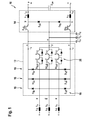
- Fig. 1 shows an electrical converter 10 comprising two converter stages 12, 14 in the form of an input voltage selector 12 and an output converter 14.
- the electrical converter 10 of Fig. 1 is an AC-to-DC converter having three phase inputs a, b, c for connecting to an electrical grid and two DC outputs p, n, which for example may be connected with a DC bus bar of a battery charging station.
- the input voltage selector 12 also has three phase inputs a , b , c , which are interconnected via the phase inductors L f with the phase inputs a, b, c, and three outputs x, y, z. These outputs may be seen as an upper voltage node x, a middle voltage node y and a lower voltage node z.
- the input voltage selector 12 connects the upper voltage node x to the phase input a, b, c with the highest voltage of the three-phase AC input voltage, the lower voltage node z to a phase input a, b, c with the lowest voltage of the three-phase AC input voltage, and the middle voltage node y to the phase input a, b, c having a voltage between the highest voltage and the lowest voltage.
- the input voltage selector 12 comprises three selector legs 16, each of which interconnects one of the phase inputs a , b , c with the nodes x, y, z.
- Each selector leg 16 comprises a half-bridge 18 (in case of Fig. 1 of diodes) interconnecting the nodes x and z, and an injector switch unit 20 (S aya , S byb and S cyc ) connected to the node y.
- the outputs x, y, z of the input voltage selector 16 are the inputs of the output converter 14, which in the embodiment of Fig.1 comprises two DC-DC buck converters and a DC output capacitor C pn .
- the switches of the output converter 14 may be switched with a PWM (pulse width modulation) scheme to generate a DC voltage between the outputs p, n.
- Three AC capacitors C x , C y , C z are connected between the nodes x, y, z. Note that in Fig. 1 , the capacitors C x , C y , C z are star-connected, while in Fig. 2 the capacitors C x , C y , C z are delta-connected. However, a delta-connection is also possible in Fig. 1 or a star-connection in Fig. 2 . In general, the three capacitors C x , C y , C z should have equal capacitance, in order to symmetrically load the AC grid. This may be required as the voltages at nodes x, y and z are piece-wise sinusoidal and form a three-phase system within every 60 0 sector of the AC input voltage.
- phase inductors and the capacitors C x , C y , C z may be seen as an electrical filter that is split into two parts by the input voltage selector 12.
- the structure of the proposed circuit with the capacitors on the output side of the input voltage selector 12 has several advantages: It shortens the commutation loops of the output converters 14, which means that no additional capacitors are required. Furthermore, the currents i x , i y and i z flowing through the input voltage selector 12 are continuous with these filter capacitors C x , C y , C z . This leads to a reduction of conduction losses in the switches of the input voltage selector 12. Additionally, the capacitors decouple the switching operations of the input voltage selector 12 and the output converter 14. Finally, in the proposed circuit, the distortions in the AC side input currents i a , i b and i c can be prevented by properly modulating the switches in the input voltage selector 12 as described below and above.
- Fig. 1 shows a unidirectional converter 10
- Fig. 2 shows a bidirectional converter 10, in which the diodes in the input voltage selector 12 and the output converter 14 have been supplemented with controllable semiconductor switches.
- a full bidirectional solution may be obtained by connecting active switches in parallel with the diodes and by connecting diodes in parallel with the existent active switches.
- the outputs x, y, z of the input voltage selector 12 are connected via inductors L f with the capacitors C x , C y , C z .
- the whole electrical LC filter may be arranged between the input voltage selector 12 and the output converter.
- Fig. 3A, 3B , 3C, 3D show different variants of a unidirectional input voltage selector 12a, 12b, 12c, 12d, which may be used in Fig. 1 .
- 12a and 12c may be made bidirectional by connecting active switches in parallel with the diodes D ax , D bx , D cx , D za , D zb and D zc .
- the injector switch unit 20 is connected via a middle point of the respective half-bridge 18 with the node y. In the input selector 12b, the injector switch unit 20 is integrated into the respective half-bridge 18.
- the injector switch units 20 of Fig. 1 and 2 have two switches connected in antiseries
- the injector switch units 20 of Fig. 3A and 3B have one switch interconnected with four diodes.
- Fig. 3C and 3D show input voltage selector 12c and 12d with a further half-bridge used as injector switch unit 20 per selector leg 16.
- an active half-bridge 18 is connected to the phase input, while a passive (diode) half-bridge 20 is connected to the middle voltage node y.
- Fig. 3D is vice versa.
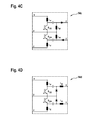
- Fig. 4A to 4D show further embodiments 14a to 14f for the output converter stage providing a DC output voltage at outputs p, n.
- a full bidirectional converter 10 may be obtained by connecting active switches in parallel with the circuit diodes and by connecting diodes in parallel with the existent active switches.
- the output converter 14 may be or may comprise a boost converter 14a, a non-inverting boost converter 14b, a SEPIC converter 14c, a Cuk converter 14d with inversed output voltage, an inverting buck-boost converter 14e with reversed output voltage, and/or two interleaved buck converters 14f.
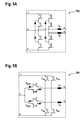
- Fig. 5A to 5D show further embodiments 14g to 14j for the output converter stage providing a DC output voltage at outputs p, n based on three-level circuit topologies.
- the output converters 14g and 14h support AC-to-DC power transfer only, which means that if the output power is reversed, the load current has to be reversed as well. If additional diodes are added as shown with output converters 14i and 14j, bidirectional power transfer is possible, provided a bidirectional input voltage selector 12 is also used.
- Output converters 14g and 14i are NPC (neutral point clamped) based, while 14h and 14j are T-type based.
- the output converters 14a to 14j are all non-isolating.
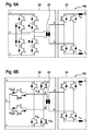
- Fig. 6A and 6B show isolating output converters 14k, 141, which comprise an isolating transformer 22 between two subconverters 24.
- output converter 14k an NPC based full-bridge configuration and in output converter 141 a T-type configuration of switches on the transformer's primary side are used.
- an active conventional full-bridge circuit is implemented, however, a simple diode bridge also may be implemented.
- the secondary side circuit 24 such as current doubler, voltage doubler, etc. may be used.
- the secondary side circuit may be like the ones shown in Fig. 6A or 6B , but with the semiconductor switches replaced by diodes.
- the electrical converter provides a one phase or three-phase output voltage as shown in Fig. 7A and 7B , which show output converters 14m, 14n with AC output.
- 14m is a non-isolated converter based on NPC bridge legs and 14n is a non-isolating converter based on T-type bridge legs.
- Fig. 1 to 7B instead of parallel diodes to a semicoductor switch, anti-parallel diodes inside each IGBT may be used.
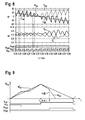
- Fig. 8 shows a diagram with the voltage u ab between the phase inputs a and b, the voltage u ab between the phase inputs a , b and the voltage u xy between the upper voltage node x and the middle voltage node y.
- the middle part of Fig. 8 shows the phase currents i a and i b and the lower part shows the switching instants/control signals of the switches (injector switch units 20) S a y a , S b y b of the input voltage selector 12 and switches S x p , S n z of the output converter 12.
- the voltage u ab is zero, when the corresponding voltages in the phases a, b cross.
- the other voltages show that there are voltage ripples with a length of the switching cycle of the output converter 14 caused due to the switching of the switches S x p , S n z of the output converter 12.
- the AC input current distortions may have a significant contribution to the current THD of the electrical converter 10. These distortions can be prevented by properly modulating the switches in the input voltage selector 12 as described in the following.
- the capacitors C x , C y , C z would be interconnecting the phase inputs a , b , c of the input voltage selector 12, the cause of the current distortions is the switching frequency voltage ripple across these capacitors and the fact that the voltages u xy and u yz cannot be negative.
- the filter capacitors C x , C y , C z have been moved to the DC side of the input voltage selector 12.
- the input voltage selector 12 can be used to temporarily disconnect the filter capacitors C x , C y , C z from the filter inductors L f by simultaneously turning on two of the three injector switch units 20, e.g. S a y a and S b y b as shown in Fig. 8 (this short-circuits the corresponding phase inputs a and b). Therefore, it is possible to mitigate the current distortions by toggling the second injection switch such that the average over one switching period of voltage u ab equals the grid voltage, i.e. u ab .
- Fig. 8 shows that S a y a is switched on and off during a number of switching cycles before the zero-crossing and is switched on after the zero-crossing.
- S b y b is switched on before the zero-crossing and is switched on and off during a number of switching cycles after the zero-crossing.
- Fig. 9 shows a diagram with one switching cycle of the output converter 12.
- the diagram shows a model of the filter capacitor voltage u xy during the first half of the first intersection ( ⁇ t ⁇ ⁇ /3, u a > u b ).
- the additional injection switch S a y a is turned on at time ⁇ ' and is turned off together with S x p in order to allow the capacitor with u xy to charge.
- Fig. 10 shows a diagram analogously to Fig. 8 . Contrary to Fig. 8 , a whole oscillation of the input voltages u a , u b , u c is depicted. In the lower part of Fig. 10 , it is indicated that the switches of the input voltage selector are not simply switched from on to off and vice versa during the corresponding crossing of the AC input voltages. They are switched on and off according to the control method as described above, thus the current distortions in the currents i a , i b , i c in the vicinity of the crossings are mitigated.
- Fig. 11 shows a further electrical converter 10, which may have an input voltage selector 12 and an output converter 14 as described above.
- the output converter 14 has a common mode filter 26 connected to its two DC outputs p, n.
- the common mode filter 26 comprises a common mode inductor L CM with a winding in each output p, n and a common core.
- the common mode filter 26 comprises two series connected common mode capacitors C CM1 , C CM2 , which are connecting the two outputs p, n.
- the point between the two capacitors C CM1 , C CM2 may be connected to the star-point of the capacitors C x , C y , C z interconnecting the nodes x, y, z between the input voltage selector 12 and the output converter 14.
Landscapes
- Engineering & Computer Science (AREA)
- Power Engineering (AREA)
- Rectifiers (AREA)
Abstract
Description
- The invention relates to the field of current conversion. In particular, the invention relates to an electrical converter and a method for controlling the electrical converter.
- For example, during charging of electrical vehicles, current conversion between an AC voltage from an electrical grid into a DC voltage takes place and the DC voltage is then provided to the battery to be charged. For example, an electrical converter may convert a three-phase AC voltage and may supply it to a DC bus, to which several batteries may be connected. Also data centres and telco sites usually need such an AC-to-DC conversion. In general, low voltage (about 400 V) DC distribution systems and DC micro grids typically require AC-to-DC conversion from an existing AC electrical grid.
- Typically, if the voltage on the DC bus is lower than the full-wave rectified AC voltage, electrical converters with two stages are used. Such electrical converters may comprise a boost-type power factor correction (PFC) stage with a 700V - 800V DC output connected in series with a DC-DC converter to achieve the desired lower DC bus voltage. Buck-type PFC converters are an alternative, allowing a single-stage energy conversion between the three-phase mains and a DC bus with lower voltage.
- For example, J. W. Kolar and T. Friedli, "The Essence of Three-Phase PFC Rectifier Systems - Part I," IEEE Transactions on Power Electronics, vol. 28, no. 1, pp. 176-198, Jan 2013; and T. Soeiro, T. Friedli and J. W. Kolar, "Three-phase high power factor mains interface concepts for Electric Vehicle battery charging systems," in Applied Power Electronics Conference and Exposition (APEC), Feb 2012, pp. 2603-2610, show electrical converters, which are adapted for AC to low voltage DC conversion.
- It is an objective of the present invention to provide a low cost and simple designed electrical converter for AC-to-DC power conversion, which generates low current distortions at its input.
- This objective is achieved by the subject-matter of the independent claims. Further exemplary embodiments are evident from the dependent claims and the following description.
- An aspect of the invention relates to an electrical converter, which, for example may be used for converting a three-phase AC voltage from an electrical grid (which may be a medium voltage, i.e. more than 1.000 kV into a low AC or DC output voltage, i.e. below 1.000 kV).
- According to an embodiment of the invention, the electrical converter comprises an input voltage selector for converting a three-phase AC input voltage provided at three phase inputs of the electrical converter into an intermediate three-phase voltage provided at an upper voltage node, a middle voltage node and a lower voltage node; capacitors interconnecting an upper voltage node, a middle voltage node and a lower voltage node; and an output converter for converting the intermediate three-phase voltage into an output voltage.
- The input voltage selector, which may be seen as a first converter stage, is adapted for connecting the upper voltage node to a phase input with the highest voltage of the three-phase AC input voltage, the lower voltage node to a phase input with the lowest voltage of the three-phase AC input voltage, and the middle voltage node to the phase input having a voltage between the highest voltage and the lowest voltage. In other words, the input voltage selector may convert the three sinusoidal AC input voltages into three piece-wise sinusoidal voltages provided at the upper voltage, middle voltage and lower voltage node.
- The output converter, which may be seen as a second converter stage and/or which may have different topologies (see below) may convert these piece-wise sinusoidal voltages into a DC voltage or a further AC voltage of different voltage magnitude and/or different frequency.
- Furthermore, three or more capacitors may be arranged between the input voltage selector and the output converter. These capacitors may be seen as (a part of) an input filter for the output converter. These capacitors may interconnect the upper voltage, middle voltage and lower voltage node.
- Since the capacitors are arranged behind (and not before) the input voltage selector from the point of the view of the phase inputs of the electrical converter (and an electrical grid connected to these phase inputs), the current distortions at the intersection of phase voltages in the phase inputs, which are mainly caused by switching voltage ripples across the capacitors, may be better controlled. For example, with the method described below, the electrical converter may be controlled such that the current distortions caused by the switching of the output converter are suppressed by switching the input voltage selector in a specific way, when two of the phase voltages in the phase inputs cross.
- According to an embodiment of the invention, the upper voltage node, the middle voltage node and the lower voltage node are star-connected and/or are delta-connected via the capacitors. Each node may be directly connected via a capacitor with both of the other nodes or may be connected with a capacitor via a star-point with the other nodes.
- According to an embodiment of the invention, a filter inductor is interconnected in each phase input. These filter inductors and the capacitors may be seen as parts of a (split) LC-filter before the input of the output converter. The input voltage selector may be seen as interconnected in this electrical filter.
- According to an embodiment of the invention, each of the upper voltage node, the middle voltage node and the lower voltage node is connected via a filter inductor with the capacitors interconnecting the upper voltage node, the middle voltage node and the lower voltage node.
- There are several embodiments of how the input voltage selector may be designed to achieve the above-mentioned distribution of the three sinusoidal AC input voltages into the three piece-wise sinusoidal voltages provided at the high, middle and lower voltage node.
- According to an embodiment of the invention, the input voltage selector comprises three selector legs for interconnecting one of the phase inputs with the upper voltage node, the middle voltage node and the lower voltage node, each selector leg comprising a half-bridge and an injector switch unit, the half-bridge connected to the upper voltage node and lower voltage node and the injector switch unit connected to the middle voltage node.
- It has to be noted that the injector switch unit also may be provided in the form of a half-bridge. For example, each selector leg may comprise two half-bridges in parallel.
- According to an embodiment of the invention, the half-bridge comprises diodes and/or the half-bridge comprises controllable semiconductor switches. When the electrical converter is a unidirectional converter, the half-bridge may be a diode-half-bridge. When the electrical converter is a bidirectional converter, these diodes may have to be substituted with semiconductor switches to allow a power transfer towards the phase inputs.
- There are also several possibilities, how the phase inputs are connected with the injector switch unit.
- According to an embodiment of the invention, the injector switch unit comprises two series-connected semiconductor switches, which are reverse to each other, the injector switch unit comprises one controllable semiconductor switch interconnected in parallel with two pairs of two series-connected diodes and/or the injector switch unit comprises a half-bridge of diodes and/or controllable semiconductor switches.
- According to an embodiment of the invention, the injector switch unit interconnects a middle point of the half-bridge with the middle voltage node or the injector switch unit is interconnected between arms of the half-bridge.
- According to an embodiment of the invention, the output converter is a DC-to-DC converter or a DC-to-AC converter. The output converter may be adapted for converting the piece-wise sinusoidal voltage provided at the nodes at the output of the input selector in a DC voltage or into a possibly multi-phase AC voltage. In the case of a DC-to-DC conversion, the electrical converter may be used for DC-distribution systems, datacenter and battery charging.
- The output converter may have many possible topologies, for example, it may be or may comprise at least one of: a simple buck or boost converter, a buck-boost converter, a non-inverting buck-boost converter, a SEPIC converter, a Cuk converter, an inverting buck-boost converter, and/or interleaved buck or boost converters.
- According to an embodiment of the invention, the output converter comprises three-level half-bridges; and/or wherein the half-bridges are NPC based or T-type based.
- According to an embodiment of the invention, the output converter is an isolated output converter comprising a transformer between two subconverter units.
- According to an embodiment of the invention, a common mode filter is provided at an output of the output converter. For example, the output converter may have two DC outputs, which may be coupled with a common mode inductor and/or a common mode capacitor.
- According to an embodiment of the invention, a star-point of the capacitors interconnecting the upper voltage node, the middle voltage node and the lower voltage node is connected with the common mode filter. For example, the common mode filter may comprise two series connected common mode capacitors, which are interconnecting two outputs of the output converter. The point between the two capacitors may be connected to the star-point of the capacitors interconnecting the upper voltage node, the middle voltage node and the lower voltage node.
- A further aspect of the invention relates to a method for controlling an electrical converter as described in the above and in the following. For example, the method may be performed by a controller, which based on measurements in the electrical converter determines switching instants of semiconductor switches of the electrical converter.
- The measurements may provide information on currents as input currents, intermediate currents and/or output currents as well as voltages, such as input (grid) voltages, intermediate voltages, capacitor voltages and/or output voltages in the electrical converter.
- It has to be understood that features of the method as described in the above and in the following may be features of the electrical converter as described in the above and in the following and vice versa.
- According to an embodiment of the invention, the method comprises: switching semiconductor switches of the input voltage selector such that the upper voltage node is connected to the phase input with the highest voltage of the three-phase AC input voltage, the lower voltage node is connected to the phase input with the lowest voltage of the three-phase AC input voltage, and the middle voltage node is connected to the phase input with a voltage between the highest voltage and the lowest voltage; wherein, when two of the voltages of the three-phase AC input voltage are crossing, the semiconductor switches of the input voltage selector are switched such that the corresponding two phase inputs are short-circuited for a specific duration in order to lower current distortions in the phase inputs of the electrical converter.
- In general, the controller may switch the semiconductor switches of the input voltage selector, such that the highest, intermediate and lowest voltage provided at the phase inputs (for example by an electrical grid) is provided to the highest voltage node, middle voltage node and lowest voltage node. Furthermore, the controller may switch semiconductor switches of the output converter (for example with a PWM scheme) such that the (piece-wise sinusoidal) voltages at the nodes are converted into a DC or AC output voltage.
- Because the capacitors of the input filter have been moved from the phase input of the input voltage selector to its output, i.e. between the input voltage selector and the output converter, the input voltage selector may be used to mitigate current distortions at the phase inputs of the electrical converter. To achieve this, the controller may switch semiconductor switches of the input voltage selector such that during the crossing of the input phases, the phase inputs of the crossing phases are short circuited, which may cancel at least partially the current distortions.
- It has to be understood that the crossing of phases not only may relate to the point, where the two phase voltages are equal but also to the vicinity of this point, for example a time interval.
- According to an embodiment of the invention, the electrical converter comprises phase inductors, each phase inductor interconnected between a phase input of the electrical converter and a respective phase input of the input voltage selector, wherein the two phase inputs of the electrical converter and the corresponding phase inductors are short-circuited such that a voltage average of a voltage between the corresponding phase inputs of the input voltage selector equals a grid voltage provided between the two phase inputs of the electrical converter.
- The electrical converter may comprise phase inductors at its phase inputs, which together with the capacitors at the output of the input voltage selector may form a split electrical filter. During the short-circuiting of two phases, the voltages at the phase inputs of the electrical converter may equalize via the phase inductors in such a way that a current reverse to a current distortion is generated, which mitigates the current distortion.
- According to an embodiment of the invention, the specific duration, during which the two phase inputs are short-circuited is determined such that during each switching cycle of a PWM modulation scheme of the output converter, the voltage average equals a grid voltage provided between the two phase inputs of the electrical converter. In such a way, the short-circuiting takes place every switching cycle, i.e. the corresponding switch of the input voltage selector is toggled on and off every switching cycle.
- According to an embodiment of the invention, the time at which the two phase inputs are short-circuited is determined based on a time, at which a semiconductor switch of an output side DC-DC converter is switched based on a PWM modulation scheme. In other words, the switching time is not determined on the beginning of the switching cycle but on the switching time of the output converter.
- The above features of the control method have been described with respect to unidirectional conversion with power transfer in the direction from the voltage input selector to the output converter. In the case, the electrical converter is a bidirectional converter, also a power transfer in the reverse direction is possible and current distortions may be mitigated by correspondingly switching semiconductor switches of the input voltage selector.
- These and other aspects of the invention will be apparent from and elucidated with reference to the embodiments described hereinafter.
- The subject-matter of the invention will be explained in more detail in the following text with reference to exemplary embodiments which are illustrated in the attached drawings.
-
Fig. 1 schematically shows a unidirectional converter according to an embodiment of the invention. -
Fig. 2 schematically shows a bidirectional converter according to an embodiment of the invention. -
Fig. 3A, 3B ,3C, 3D schematically show embodiments of input voltage selectors for an electrical converter according to an embodiment of the invention. -
Fig. 4A, 4B ,4C, 4D ,4E, 4F schematically show embodiments of output converters for an electrical converter according to an embodiment of the invention. -
Fig. 5A, 5B ,5C, 5D schematically show embodiments of output converters for an electrical converter according to an embodiment of the invention. -
Fig. 6A, 6B schematically show embodiments of output converters for an electrical converter according to an embodiment of the invention. -
Fig. 7A, 7B schematically show embodiments of output converters for an electrical converter according to an embodiment of the invention. -
Fig. 8 shows a diagram with voltages, currents and switching states during a crossing of two phase voltages, which illustrates a control method according to an embodiment of the invention. -
Fig. 9 shows a diagram with voltages and switching states during a switching cycle of the electrical converter. -
Fig. 10 shows a diagram with voltages, currents and switching states during a complete oscillation of the input phases, which illustrates a control method according to an embodiment of the invention. -
Fig. 11 schematically shows a converter according to a further embodiment of the invention. - In principle, identical parts are provided with the same reference symbols in the figures.
-
Fig. 1 shows anelectrical converter 10 comprising twoconverter stages input voltage selector 12 and anoutput converter 14. Theelectrical converter 10 ofFig. 1 is an AC-to-DC converter having three phase inputs a, b, c for connecting to an electrical grid and two DC outputs p, n, which for example may be connected with a DC bus bar of a battery charging station. - The
input voltage selector 12 also has three phase inputsa ,b ,c , which are interconnected via the phase inductors Lf with the phase inputs a, b, c, and three outputs x, y, z. These outputs may be seen as an upper voltage node x, a middle voltage node y and a lower voltage node z. - The
input voltage selector 12 connects the upper voltage node x to the phase input a, b, c with the highest voltage of the three-phase AC input voltage, the lower voltage node z to a phase input a, b, c with the lowest voltage of the three-phase AC input voltage, and the middle voltage node y to the phase input a, b, c having a voltage between the highest voltage and the lowest voltage. To achieve this, theinput voltage selector 12 comprises threeselector legs 16, each of which interconnects one of the phase inputsa ,b ,c with the nodes x, y, z. - Each
selector leg 16 comprises a half-bridge 18 (in case ofFig. 1 of diodes) interconnecting the nodes x and z, and an injector switch unit 20 (Saya, Sbyb and Scyc) connected to the node y. - The outputs x, y, z of the
input voltage selector 16 are the inputs of theoutput converter 14, which in the embodiment ofFig.1 comprises two DC-DC buck converters and a DC output capacitor Cpn . For example, the switches of theoutput converter 14 may be switched with a PWM (pulse width modulation) scheme to generate a DC voltage between the outputs p, n. - Three AC capacitors Cx, Cy, Cz are connected between the nodes x, y, z. Note that in
Fig. 1 , the capacitors Cx, Cy, Cz are star-connected, while inFig. 2 the capacitors Cx, Cy, Cz are delta-connected. However, a delta-connection is also possible inFig. 1 or a star-connection inFig. 2 . In general, the three capacitors Cx, Cy, Cz should have equal capacitance, in order to symmetrically load the AC grid. This may be required as the voltages at nodes x, y and z are piece-wise sinusoidal and form a three-phase system within every 600 sector of the AC input voltage. - The phase inductors and the capacitors Cx, Cy, Cz may be seen as an electrical filter that is split into two parts by the
input voltage selector 12. - The structure of the proposed circuit with the capacitors on the output side of the
input voltage selector 12 has several advantages: It shortens the commutation loops of theoutput converters 14, which means that no additional capacitors are required. Furthermore, the currents ix, iy and iz flowing through theinput voltage selector 12 are continuous with these filter capacitors Cx, Cy, Cz. This leads to a reduction of conduction losses in the switches of theinput voltage selector 12. Additionally, the capacitors decouple the switching operations of theinput voltage selector 12 and theoutput converter 14. Finally, in the proposed circuit, the distortions in the AC side input currents ia, ib and ic can be prevented by properly modulating the switches in theinput voltage selector 12 as described below and above. -
Fig. 1 shows aunidirectional converter 10, whileFig. 2 shows abidirectional converter 10, in which the diodes in theinput voltage selector 12 and theoutput converter 14 have been supplemented with controllable semiconductor switches. A full bidirectional solution may be obtained by connecting active switches in parallel with the diodes and by connecting diodes in parallel with the existent active switches. - Furthermore, as shown in
Fig. 2 , it may be possible that the outputs x, y, z of theinput voltage selector 12 are connected via inductors Lf with the capacitors Cx, Cy, Cz. Thus, the whole electrical LC filter may be arranged between theinput voltage selector 12 and the output converter. -
Fig. 3A, 3B ,3C, 3D show different variants of a unidirectionalinput voltage selector Fig. 1 . 12a and 12c may be made bidirectional by connecting active switches in parallel with the diodes Dax, Dbx, Dcx, Dza, Dzb and Dzc. - In the
input voltage selector 12a, theinjector switch unit 20 is connected via a middle point of the respective half-bridge 18 with the node y. In theinput selector 12b, theinjector switch unit 20 is integrated into the respective half-bridge 18. - While the
injector switch units 20 ofFig. 1 and2 have two switches connected in antiseries, theinjector switch units 20 ofFig. 3A and 3B have one switch interconnected with four diodes. -
Fig. 3C and 3D showinput voltage selector injector switch unit 20 perselector leg 16. InFig. 3C , an active half-bridge 18 is connected to the phase input, while a passive (diode) half-bridge 20 is connected to the middle voltage node y.Fig. 3D is vice versa. -
Fig. 4A to 4D show further embodiments 14a to 14f for the output converter stage providing a DC output voltage at outputs p, n. Again, a fullbidirectional converter 10 may be obtained by connecting active switches in parallel with the circuit diodes and by connecting diodes in parallel with the existent active switches. - In general, the
output converter 14 may be or may comprise aboost converter 14a, anon-inverting boost converter 14b, aSEPIC converter 14c, aCuk converter 14d with inversed output voltage, an inverting buck-boost converter 14e with reversed output voltage, and/or two interleavedbuck converters 14f. -
Fig. 5A to 5D showfurther embodiments 14g to 14j for the output converter stage providing a DC output voltage at outputs p, n based on three-level circuit topologies. By using three-level circuit topologies for the output converter stage, a circuit solution with switchable output voltage polarity can be built. Theoutput converters output converters input voltage selector 12 is also used.Output converters - The
output converters 14a to 14j (and also 14m and 14n below) are all non-isolating. -
Fig. 6A and 6B show isolatingoutput converters transformer 22 between twosubconverters 24. Inoutput converter 14k, an NPC based full-bridge configuration and in output converter 141 a T-type configuration of switches on the transformer's primary side are used. On the transformer's secondary side, an active conventional full-bridge circuit is implemented, however, a simple diode bridge also may be implemented. - Other configurations for the
secondary side circuit 24 such as current doubler, voltage doubler, etc. may be used. For example, the secondary side circuit may be like the ones shown inFig. 6A or 6B , but with the semiconductor switches replaced by diodes. - It also may be possible that the electrical converter provides a one phase or three-phase output voltage as shown in
Fig. 7A and 7B , which showoutput converters - In
Fig. 1 to 7B , instead of parallel diodes to a semicoductor switch, anti-parallel diodes inside each IGBT may be used. - With respect to
Fig. 8, 9 and10 , a method of controlling theelectrical converter 10 is described. - In the upper part,
Fig. 8 shows a diagram with the voltage uab between the phase inputs a and b, the voltage uab between the phase inputsa ,b and the voltage uxy between the upper voltage node x and the middle voltage node y. The middle part ofFig. 8 shows the phase currents ia and ib and the lower part shows the switching instants/control signals of the switches (injector switch units 20) Sa ya , Sb yb of theinput voltage selector 12 and switches Sxp , Sn z of theoutput converter 12. - The voltage uab is zero, when the corresponding voltages in the phases a, b cross. The other voltages show that there are voltage ripples with a length of the switching cycle of the
output converter 14 caused due to the switching of the switches Sxp , Sn z of theoutput converter 12. - The AC input current distortions may have a significant contribution to the current THD of the
electrical converter 10. These distortions can be prevented by properly modulating the switches in theinput voltage selector 12 as described in the following. - In the case, the capacitors Cx, Cy, Cz would be interconnecting the phase inputs
a ,b ,c of theinput voltage selector 12, the cause of the current distortions is the switching frequency voltage ripple across these capacitors and the fact that the voltages uxy and uyz cannot be negative. - Therefore, the filter capacitors Cx, Cy, Cz have been moved to the DC side of the
input voltage selector 12. In such a way, theinput voltage selector 12 can be used to temporarily disconnect the filter capacitors Cx, Cy, Cz from the filter inductors Lf by simultaneously turning on two of the threeinjector switch units 20, e.g. Sa ya and Sb yb as shown inFig. 8 (this short-circuits the corresponding phase inputsa and b). Therefore, it is possible to mitigate the current distortions by toggling the second injection switch such that the average over one switching period of voltage uab equals the grid voltage, i.e. uab . - For example,
Fig. 8 shows that Sa ya is switched on and off during a number of switching cycles before the zero-crossing and is switched on after the zero-crossing. On the other hand, Sb yb is switched on before the zero-crossing and is switched on and off during a number of switching cycles after the zero-crossing. - The following considerations focus on the power transfer from the
input voltage selector 12 towards theoutput converter 14 and the intersection of ua and ub at ωt=π/3. However, they can be generalized for the other five intersections (shown inFig. 10 ) and power transfer from theoutput converter 14 towards theinput voltage selector 12. - First of all, it can be seen from
Fig. 8 that uxy increases while Sxp is not conducting, which implies that uxy is minimal when Sxp is turned off. Therefore, the turn-off of Sxp is selected as origin for the auxiliary time axis τ. -
Fig. 9 shows a diagram with one switching cycle of theoutput converter 12. The diagram shows a model of the filter capacitor voltage uxy during the first half of the first intersection (ωt ≈ π/3, ua > ub ). The additional injection switch Sa ya is turned on at time τ' and is turned off together with Sxp in order to allow the capacitor with uxy to charge. - In order to simplify analytical calculations u'xy is used as an approximation for uxy :


dp may be seen as the switching cycle of Sxp. The average 〈uab (τ)〉 Ts over one switching frequency period Ts of the IVS output voltage uab can be found by integration:
- In order to prevent the current distortions τ' has to be selected such that 〈u
ab (τ)〉 Ts equals the corresponding AC grid voltage uab which is used as reference value uref :
- By solving (4) an algebraic expression for τ' can be found:

- This implies that the current distortions can be mitigated by measuring the grid voltages and by evaluating equations (3), (5) and (6) every switching frequency cycle. The additional injection switch S
a ya is then turned on at time τ' after turn-off of Sxp . - All considerations and calculations given above hold only for the first half of the first sliding intersection, i.e. for ωt<π/3. In the second half (ωt>π/3), the grid voltage uab becomes negative which implies that the output voltage of the
input voltage selector 12 has to be negative as well, while the filter capacitor voltage uxy remains positive. This is achieved by modulating Sb yb instead of Sa ya as can be seen inFig. 9 . - By replacing the grid voltages ua and ub and the injection switches with the corresponding values, this can be generalized for the other two positive grid voltage intersections (ωt= 1800; 3000). Furthermore, the concept can be expanded to the negative side of the output converter 14 (Snz , dn, uyz) to mitigate the current distortions at the intersections of negative grid voltages (ωt=00; 1200; 2400). The resulting formulas are summarized in the following tables.
AC-to-DC Power Transfer Positive Voltage Intersections Origin of τ': Sx p 1 → 0Modulation: S a ya , Sb yb , Sc yc 
In-Phase Carriers: 
Interleaved Carriers: 
Negative Voltage Intersections Origin of τ':S n z 1 → 0Modulation: S a ya , Sb yb , Sc yc 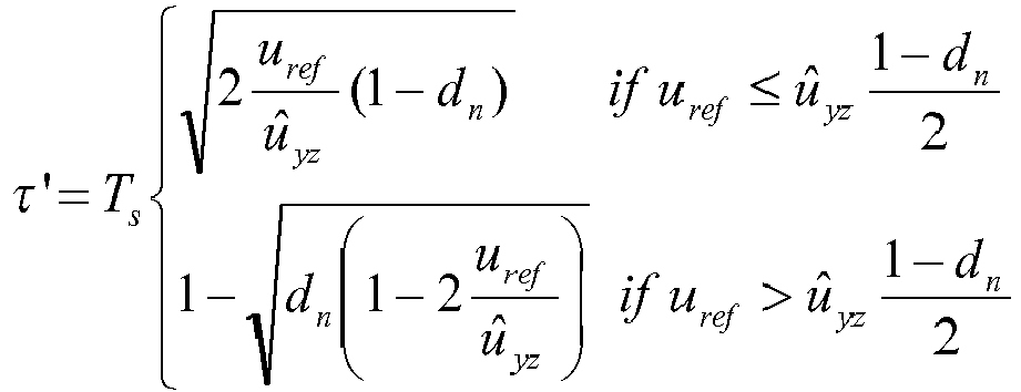
In-Phase Carriers: 
Interleaved Carriers: 
DC-to-AC Power Transfer Positive Voltage Intersections Origin of τ':Sx p 0 → 1Modulation: Sx a , Sxb , Sxc 
In-Phase Carriers: 
Interleaved Carriers: 
Negative Voltage Intersections Origin of τ':S n z 0→1Modulation: S a z , Sb z , Sc z
In-Phase Carriers: 
Interleaved Carriers: 
-
Fig. 10 shows a diagram analogously toFig. 8 . Contrary toFig. 8 , a whole oscillation of the input voltages ua, ub, uc is depicted. In the lower part ofFig. 10 , it is indicated that the switches of the input voltage selector are not simply switched from on to off and vice versa during the corresponding crossing of the AC input voltages. They are switched on and off according to the control method as described above, thus the current distortions in the currents ia, ib, ic in the vicinity of the crossings are mitigated. -
Fig. 11 shows a furtherelectrical converter 10, which may have aninput voltage selector 12 and anoutput converter 14 as described above. InFig. 11 , theoutput converter 14 has acommon mode filter 26 connected to its two DC outputs p, n. In particular, thecommon mode filter 26 comprises a common mode inductor LCM with a winding in each output p, n and a common core. Furthermore, thecommon mode filter 26 comprises two series connected common mode capacitors CCM1, CCM2, which are connecting the two outputs p, n. - The point between the two capacitors CCM1, CCM2 may be connected to the star-point of the capacitors Cx, Cy, Cz interconnecting the nodes x, y, z between the
input voltage selector 12 and theoutput converter 14. - It may be possible that further filter inductors Lp, Ln are provided in the outputs p, n and that a further DC link capacitor Cpn is interconnecting the outputs p, n.
- While the invention has been illustrated and described in detail in the drawings and foregoing description, such illustration and description are to be considered illustrative or exemplary and not restrictive; the invention is not limited to the disclosed embodiments. Other variations to the disclosed embodiments can be understood and effected by those skilled in the art and practising the claimed invention, from a study of the drawings, the disclosure, and the appended claims. In the claims, the word "comprising" does not exclude other elements or steps, and the indefinite article "a" or "an" does not exclude a plurality. A single processor or controller or other unit may fulfil the functions of several items recited in the claims. The mere fact that certain measures are recited in mutually different dependent claims does not indicate that a combination of these measures cannot be used to advantage. Any reference signs in the claims should not be construed as limiting the scope.
Claims (15)
- An electrical converter (10), comprising:an input voltage selector (12) for converting a three-phase AC input voltage provided at three phase inputs (a, b, c) of the electrical converter into an intermediate three-phase voltage provided at an upper voltage node (x), a middle voltage node (y) and a lower voltage node (z);capacitors (Cx, Cy, Cz) interconnecting an upper voltage node (x), a middle voltage node (y) and a lower voltage node (z);an output converter (14) for converting the intermediate three-phase voltage into an output voltage;wherein the input voltage selector (12) is adapted for connecting the upper voltage node (x) to a phase input (a, b, c) with the highest voltage of the three-phase AC input voltage, the lower voltage node (z) to a phase input (a, b, c) with the lowest voltage of the three-phase AC input voltage, and the middle voltage node (y) to the phase input (a, b, c) having a voltage between the highest voltage and the lowest voltage.
- The electrical converter (10) of claim 1,
wherein the upper voltage node (x), the middle voltage node (y) and the lower voltage (z) node are star-connected via the capacitors (Cx, Cy, Cz); and/or
wherein the upper voltage node (x), the middle voltage node (y) and the lower voltage node (z) are delta-connected via the capacitors (Cx, Cy, Cz). - The electrical converter (10) of claim 1 or 2,
wherein a filter inductor (Lf) is interconnected in each phase input (a, b, c); and/or wherein each of the upper voltage node (x), the middle voltage node (y) and the lower voltage node (z) is connected via a filter inductor (Lf) with the capacitors (Cx, Cy, Cz) interconnecting the upper voltage node (x), the middle voltage node (y) and the lower voltage node (z). - The electrical converter (10) of one of the preceding claims,
wherein the input voltage selector (12) comprises three selector legs (16) for interconnecting one of the phase inputs (a, b, c) with the upper voltage node (x), the middle voltage node (y) and the lower voltage node (z), each selector leg (16) comprising a half-bridge (18) and an injector switch unit (20), the half-bridge (18) connected to the upper voltage node (x) and lower voltage node (z) and the injector switch unit (20) connected to the middle voltage node (z), - The electrical converter (10) of claim 4,
wherein the half-bridge (18) comprises diodes; and/or
wherein the half-bridge (18) comprises controllable semiconductor switches. - The electrical converter (10) of claim 4 or 5,
wherein the injector switch unit (20) comprises two series-connected semiconductor switches, which are reverse to each other; or
wherein the injector switch unit comprises (20) one controllable semiconductor switch interconnected in parallel with two pairs of two series-connected diodes; or
wherein the injector switch unit (20) comprises a half-bridge of diodes and/or controllable semiconductor switches. - The electrical converter (10) of one of claims 4 to 6,
wherein the injector switch unit (20) interconnects a middle point of the half-bridge (18) with the middle voltage node (y); or
wherein the injector switch unit (20) is interconnected between arms of the half-bridge (18). - The electrical converter (10) of one of the preceding claims,
wherein the output converter is or comprises at least one of:a boost converter (14a),a non-inverting buck-boost converter (14b),a SEPIC converter (14c),a Cuk converter (14d),an inverting buck-boost converter (14e),interleaved buck converters (14f). - The electrical converter (10) of one of the preceding claims,
wherein the output converter is a DC-to-DC converter (14, 14a to 141) or a DC-to-AC converter (14m, 14n); and/or
wherein the output converter is an isolated output converter (14k, 141) comprising a transformer between two subconverter units. - The electrical converter (10) of one of the preceding claims,
wherein the output converter (14g to 14j, 14m, 14n) comprises three-level half-bridges; and/or
wherein the half-bridges are NPC based or T-type based. - The electrical converter (10) of one of the preceding claims,
wherein a common mode filter (26) is provided at an output (p, n) of the output converter (14); and/or
wherein a star-point of the capacitors (Cx, Cy, Cz) interconnecting the upper voltage node (x), the middle voltage node (y) and the lower voltage node (z) is connected with the common mode filter (26). - A method for controlling an electrical converter (10) according to one of the preceding claims, the method comprising:switching semiconductor switches of the input voltage selector (12) such that the upper voltage node (x) is connected to the phase input (a, b, c) with the highest voltage of the three-phase AC input voltage, the lower voltage node (z) is connected to the phase input (a, b, c) with the lowest voltage of the three-phase AC input voltage, and the middle voltage node (y) is connected to the phase input (a, b, c) with a voltage between the highest voltage and the lowest voltage;wherein, when two of the voltages of the three-phase AC input voltage are crossing, the semiconductor switches of the input voltage selector (12) are switched such that the corresponding two phase inputs (
a , b, c) are short-circuited for a specific duration in order to lower current distortions in the phase inputs (a, b, c) of the electrical converter (10). - The method of claim 12,
wherein the electrical converter (10) comprises phase inductors (Lf), each phase inductor interconnected between a phase input (a, b, c) of the electrical converter (10) and a respective phase input (a ,b ,c ) of the input voltage selector (12);
wherein the two phase inputs (a, b, c) of the electrical converter and the corresponding phase inductors are short-circuited such that a voltage average of a voltage between the corresponding phase inputs (a ,b ,c ) of the input voltage selector (12) equals a grid voltage provided between the two phase inputs (a, b, c) of the electrical converter (10). - The method of claim 13,
wherein the specific duration, during which the two phase inputs (a, b, c) are short-circuited is determined such that during each switching cycle of a PWM modulation scheme of the output converter, the voltage average equals a grid voltage provided between the two phase inputs (a, b, c) of the electrical converter (10). - The method of one of claims 12 to 14,
wherein the time at which the two phase inputs (a, b, c) are short-circuited is determined based on a time, at which a semiconductor switch of the electrical converter (10) is switched based on a PWM modulation scheme.
Priority Applications (2)
| Application Number | Priority Date | Filing Date | Title |
|---|---|---|---|
| EP15174720.1A EP3113345B1 (en) | 2015-07-01 | 2015-07-01 | Electrical converter and control method |
| ES15174720T ES2908960T3 (en) | 2015-07-01 | 2015-07-01 | Electrical converter and control method |
Applications Claiming Priority (1)
| Application Number | Priority Date | Filing Date | Title |
|---|---|---|---|
| EP15174720.1A EP3113345B1 (en) | 2015-07-01 | 2015-07-01 | Electrical converter and control method |
Publications (2)
| Publication Number | Publication Date |
|---|---|
| EP3113345A1 true EP3113345A1 (en) | 2017-01-04 |
| EP3113345B1 EP3113345B1 (en) | 2022-02-23 |
Family
ID=53510696
Family Applications (1)
| Application Number | Title | Priority Date | Filing Date |
|---|---|---|---|
| EP15174720.1A Active EP3113345B1 (en) | 2015-07-01 | 2015-07-01 | Electrical converter and control method |
Country Status (2)
| Country | Link |
|---|---|
| EP (1) | EP3113345B1 (en) |
| ES (1) | ES2908960T3 (en) |
Cited By (17)
| Publication number | Priority date | Publication date | Assignee | Title |
|---|---|---|---|---|
| WO2018126393A1 (en) | 2017-01-05 | 2018-07-12 | General Electric Company | Dc fast charging station for electric vehicles |
| WO2020089419A1 (en) * | 2018-11-02 | 2020-05-07 | Prodrive Technologies B.V. | Electrical power converter |
| CN111431394A (en) * | 2020-04-17 | 2020-07-17 | 广东工业大学 | Novel step-down single-phase three-level bridgeless PFC converter system |
| DE102019102550A1 (en) * | 2019-02-01 | 2020-08-06 | Infineon Technologies Austria Ag | PERFORMANCE CONVERTER AND PERFORMANCE CONVERSION PROCESS |
| US10917019B2 (en) | 2019-03-11 | 2021-02-09 | Utah State University | Quasi-single stage power converter topology |
| CN112532038A (en) * | 2020-10-27 | 2021-03-19 | 东南大学 | Control system and method for reducing current distortion at three-phase Stevens circuit boundary |
| CN113783453A (en) * | 2021-09-29 | 2021-12-10 | 山东建筑大学 | A low-cost high-gain three-level inverter and its space vector modulation method |
| EP3963703A1 (en) * | 2019-05-02 | 2022-03-09 | Prodrive Technologies Innovation Services B.V. | Electrical converter |
| DE102020214265A1 (en) | 2020-11-12 | 2022-05-12 | Universität Paderborn | Device for low-common-mode conversion of alternating voltage |
| US11404972B2 (en) | 2019-11-25 | 2022-08-02 | Carrier Corporation | Power module and converter with asymmetrical semiconductor rating arrangement |
| CN115102417A (en) * | 2022-06-06 | 2022-09-23 | 江苏科曜能源科技有限公司 | Four-wire three-level energy storage converter |
| DE102021206982A1 (en) | 2021-07-02 | 2023-01-05 | Universität Paderborn, Körperschaft des öffentlichen Rechts | Transformerless on-board electric vehicle charger and method for driving a DC/DC stage in a transformerless on-board electric vehicle charger |
| JP2023523865A (en) * | 2020-05-04 | 2023-06-07 | プロドライヴ・テクノロジーズ・イノヴェーション・サービシーズ・ベーフェー | Power converter with precharge mode of operation |
| CN116365890A (en) * | 2023-05-04 | 2023-06-30 | 西南交通大学 | Three-phase staggered T-shaped three-level LLC converter and wide voltage transformation control method thereof |
| WO2023234898A1 (en) * | 2022-06-01 | 2023-12-07 | Aselsan Elektroni̇k Sanayi̇ Ve Ti̇caret Anoni̇m Şi̇rketi̇ | Three-phase, three-level, transformerless, t-typ inverter with bipolar buck-boost converter on the dc side |
| DE102023211916A1 (en) * | 2023-11-29 | 2025-06-05 | Zf Friedrichshafen Ag | Charging circuit for an electrically powered motor vehicle |
| EP3830939B1 (en) * | 2018-07-31 | 2025-08-27 | Raytheon Company | Adaptive power converter topologies supporting active power factor correction (pfc) |
Citations (3)
| Publication number | Priority date | Publication date | Assignee | Title |
|---|---|---|---|---|
| US20090040800A1 (en) * | 2007-08-10 | 2009-02-12 | Maximiliano Sonnaillon | Three phase rectifier and rectification method |
| CH704553A2 (en) * | 2011-02-21 | 2012-08-31 | Eth Zuerich Eth Transfer | Alternating current/direct current (AC/DC) converter for electric vehicle, has bridge circuit comprising three connection points that are connected to DC voltage side center through four-quadrant switches respectively |
| WO2015021489A1 (en) * | 2013-08-13 | 2015-02-19 | Schneider Electric Power Drives Gmbh | Rectifier circuit having current injection |
-
2015
- 2015-07-01 EP EP15174720.1A patent/EP3113345B1/en active Active
- 2015-07-01 ES ES15174720T patent/ES2908960T3/en active Active
Patent Citations (3)
| Publication number | Priority date | Publication date | Assignee | Title |
|---|---|---|---|---|
| US20090040800A1 (en) * | 2007-08-10 | 2009-02-12 | Maximiliano Sonnaillon | Three phase rectifier and rectification method |
| CH704553A2 (en) * | 2011-02-21 | 2012-08-31 | Eth Zuerich Eth Transfer | Alternating current/direct current (AC/DC) converter for electric vehicle, has bridge circuit comprising three connection points that are connected to DC voltage side center through four-quadrant switches respectively |
| WO2015021489A1 (en) * | 2013-08-13 | 2015-02-19 | Schneider Electric Power Drives Gmbh | Rectifier circuit having current injection |
Non-Patent Citations (2)
| Title |
|---|
| J. W. KOLAR; T. FRIEDLI: "The Essence of Three-Phase PFC Rectifier Systems", IEEE TRANSACTIONS ON POWER ELECTRONICS, vol. 28, no. 1, January 2013 (2013-01-01), pages 176 - 198, XP055389125, DOI: doi:10.1109/TPEL.2012.2197867 |
| T. SOEIRO; T. FRIEDLI; J. W. KOLAR: "Three-phase high power factor mains interface concepts for Electric Vehicle battery charging systems", APPLIED POWER ELECTRONICS CONFERENCE AND EXPOSITION (APEC, February 2012 (2012-02-01), pages 2603 - 2610, XP032128034, DOI: doi:10.1109/APEC.2012.6166190 |
Cited By (31)
| Publication number | Priority date | Publication date | Assignee | Title |
|---|---|---|---|---|
| WO2018126393A1 (en) | 2017-01-05 | 2018-07-12 | General Electric Company | Dc fast charging station for electric vehicles |
| TWI766925B (en) * | 2017-01-05 | 2022-06-11 | 美商奇異電器公司 | Dc fast charging station for electric vehicles |
| US11824380B2 (en) | 2017-01-05 | 2023-11-21 | General Electric Company | DC fast charging station for electric vehicles |
| EP3566283A4 (en) * | 2017-01-05 | 2020-06-10 | General Electric Company | C.C. FAST RECHARGING STATION FOR ELECTRIC VEHICLES |
| EP3830939B1 (en) * | 2018-07-31 | 2025-08-27 | Raytheon Company | Adaptive power converter topologies supporting active power factor correction (pfc) |
| CN113287252A (en) * | 2018-11-02 | 2021-08-20 | 浦卓科技有限公司 | Power converter |
| CN113287252B (en) * | 2018-11-02 | 2024-04-09 | 浦卓科技创新服务有限公司 | Power Converters |
| NL2021926B1 (en) * | 2018-11-02 | 2020-05-14 | Prodrive Tech Bv | Electrical power converter |
| WO2020089419A1 (en) * | 2018-11-02 | 2020-05-07 | Prodrive Technologies B.V. | Electrical power converter |
| US11387730B2 (en) * | 2018-11-02 | 2022-07-12 | Prodrive Technologies Innovation Services B.V. | Electrical power converter |
| DE102019102550A1 (en) * | 2019-02-01 | 2020-08-06 | Infineon Technologies Austria Ag | PERFORMANCE CONVERTER AND PERFORMANCE CONVERSION PROCESS |
| DE102019102550B4 (en) | 2019-02-01 | 2022-06-30 | Infineon Technologies Austria Ag | POWER CONVERTERS AND POWER CONVERSION METHODS |
| US10917019B2 (en) | 2019-03-11 | 2021-02-09 | Utah State University | Quasi-single stage power converter topology |
| EP3963703A1 (en) * | 2019-05-02 | 2022-03-09 | Prodrive Technologies Innovation Services B.V. | Electrical converter |
| US11404972B2 (en) | 2019-11-25 | 2022-08-02 | Carrier Corporation | Power module and converter with asymmetrical semiconductor rating arrangement |
| CN111431394A (en) * | 2020-04-17 | 2020-07-17 | 广东工业大学 | Novel step-down single-phase three-level bridgeless PFC converter system |
| JP2023523865A (en) * | 2020-05-04 | 2023-06-07 | プロドライヴ・テクノロジーズ・イノヴェーション・サービシーズ・ベーフェー | Power converter with precharge mode of operation |
| CN112532038A (en) * | 2020-10-27 | 2021-03-19 | 东南大学 | Control system and method for reducing current distortion at three-phase Stevens circuit boundary |
| CN112532038B (en) * | 2020-10-27 | 2021-12-28 | 东南大学 | Control system and method for reducing current distortion at boundary of three-phase Schweitzer circuit |
| WO2022101396A1 (en) * | 2020-11-12 | 2022-05-19 | Universität Paderborn | Device for the low-common-mode conversion of alternating voltage |
| DE102020214265A1 (en) | 2020-11-12 | 2022-05-12 | Universität Paderborn | Device for low-common-mode conversion of alternating voltage |
| DE102021206982A1 (en) | 2021-07-02 | 2023-01-05 | Universität Paderborn, Körperschaft des öffentlichen Rechts | Transformerless on-board electric vehicle charger and method for driving a DC/DC stage in a transformerless on-board electric vehicle charger |
| EP4363263A1 (en) * | 2021-07-02 | 2024-05-08 | Universität Paderborn | Transformerless on-board charging device for electric vehicles, and method for controlling a dc/dc stage in a transformerless on-board charging device for electric vehicles |
| CN113783453A (en) * | 2021-09-29 | 2021-12-10 | 山东建筑大学 | A low-cost high-gain three-level inverter and its space vector modulation method |
| WO2023234898A1 (en) * | 2022-06-01 | 2023-12-07 | Aselsan Elektroni̇k Sanayi̇ Ve Ti̇caret Anoni̇m Şi̇rketi̇ | Three-phase, three-level, transformerless, t-typ inverter with bipolar buck-boost converter on the dc side |
| CN115102417B (en) * | 2022-06-06 | 2024-01-12 | 江苏科曜能源科技有限公司 | Four-wire three-level energy storage converter |
| CN115102417A (en) * | 2022-06-06 | 2022-09-23 | 江苏科曜能源科技有限公司 | Four-wire three-level energy storage converter |
| CN116365890B (en) * | 2023-05-04 | 2023-11-24 | 西南交通大学 | Three-phase staggered T-shaped three-level LLC converter and wide voltage transformation control method thereof |
| CN116365890A (en) * | 2023-05-04 | 2023-06-30 | 西南交通大学 | Three-phase staggered T-shaped three-level LLC converter and wide voltage transformation control method thereof |
| DE102023211916A1 (en) * | 2023-11-29 | 2025-06-05 | Zf Friedrichshafen Ag | Charging circuit for an electrically powered motor vehicle |
| DE102023211916B4 (en) * | 2023-11-29 | 2025-07-31 | Zf Friedrichshafen Ag | Charging circuit for an electrically powered motor vehicle |
Also Published As
| Publication number | Publication date |
|---|---|
| EP3113345B1 (en) | 2022-02-23 |
| ES2908960T3 (en) | 2022-05-04 |
Similar Documents
| Publication | Publication Date | Title |
|---|---|---|
| EP3113345B1 (en) | Electrical converter and control method | |
| Siwakoti et al. | A novel seven-level active neutral-point-clamped converter with reduced active switching devices and DC-link voltage | |
| Sahoo et al. | A three-level LC-switching-based voltage boost NPC inverter | |
| Khan et al. | An improved single-phase direct PWM inverting buck–boost AC–AC converter | |
| Ahmed et al. | A novel buck–boost AC–AC converter with both inverting and noninverting operations and without commutation problem | |
| Koushki et al. | Review and comparison of bi-directional AC-DC converters with V2G capability for on-board EV and HEV | |
| JP5687498B2 (en) | Power conversion system | |
| JP7309870B2 (en) | power converter | |
| Siwakoti et al. | Power electronics converters—An overview | |
| US20110280055A1 (en) | 3-phase high-power ups | |
| US20080304296A1 (en) | DC-DC and DC-AC power conversion system | |
| CN107534398B (en) | Half-bridge inverter unit and inverter | |
| US20140049998A1 (en) | DC to AC Power Converter | |
| WO2013137749A1 (en) | Electrical systems with inductive power transfer-based energy balancing | |
| Afsharian et al. | A new PWM and commutation scheme for one phase loss operation of three-phase isolated buck matrix-type rectifier | |
| US11065968B2 (en) | Integrated multi-source IPT system | |
| Valipour et al. | Extended range bridgeless PFC converter with high-voltage DC bus and small inductor | |
| Yuan | A four-level π-type converter for low-voltage applications | |
| US20150003132A1 (en) | Inverter with less snubber capacitors | |
| Ray et al. | Analysis and PWM control of three-phase boost-derived hybrid converter | |
| US20220278607A1 (en) | Electrical converter | |
| Li et al. | A boost-Full-Bridge-type single-Active-bridge isolated AC-DC converter | |
| Nayak et al. | An asymmetrical space vector PWM scheme for a three phase single-stage DC-AC Converter | |
| Gaafar et al. | Multi‐input transformer‐less four‐wire microinverter with distributed MPPT for PV systems | |
| Rizet et al. | A simplified resonant pole for three-level soft-switching PFC rectifier used in UPS |
Legal Events
| Date | Code | Title | Description |
|---|---|---|---|
| PUAI | Public reference made under article 153(3) epc to a published international application that has entered the european phase |
Free format text: ORIGINAL CODE: 0009012 |
|
| STAA | Information on the status of an ep patent application or granted ep patent |
Free format text: STATUS: THE APPLICATION HAS BEEN PUBLISHED |
|
| AK | Designated contracting states |
Kind code of ref document: A1 Designated state(s): AL AT BE BG CH CY CZ DE DK EE ES FI FR GB GR HR HU IE IS IT LI LT LU LV MC MK MT NL NO PL PT RO RS SE SI SK SM TR |
|
| AX | Request for extension of the european patent |
Extension state: BA ME |
|
| RAP1 | Party data changed (applicant data changed or rights of an application transferred) |
Owner name: ABB SCHWEIZ AG |
|
| STAA | Information on the status of an ep patent application or granted ep patent |
Free format text: STATUS: REQUEST FOR EXAMINATION WAS MADE |
|
| 17P | Request for examination filed |
Effective date: 20170703 |
|
| RBV | Designated contracting states (corrected) |
Designated state(s): AL AT BE BG CH CY CZ DE DK EE ES FI FR GB GR HR HU IE IS IT LI LT LU LV MC MK MT NL NO PL PT RO RS SE SI SK SM TR |
|
| STAA | Information on the status of an ep patent application or granted ep patent |
Free format text: STATUS: EXAMINATION IS IN PROGRESS |
|
| 17Q | First examination report despatched |
Effective date: 20181022 |
|
| GRAP | Despatch of communication of intention to grant a patent |
Free format text: ORIGINAL CODE: EPIDOSNIGR1 |
|
| STAA | Information on the status of an ep patent application or granted ep patent |
Free format text: STATUS: GRANT OF PATENT IS INTENDED |
|
| RIC1 | Information provided on ipc code assigned before grant |
Ipc: H02M 1/00 20060101ALN20210902BHEP Ipc: H02M 7/487 20070101ALN20210902BHEP Ipc: H02M 7/483 20070101ALN20210902BHEP Ipc: H02M 3/335 20060101ALN20210902BHEP Ipc: H02M 3/00 20060101ALN20210902BHEP Ipc: H02M 3/155 20060101ALN20210902BHEP Ipc: H02M 7/217 20060101ALI20210902BHEP Ipc: H02M 7/06 20060101ALI20210902BHEP Ipc: H02M 3/158 20060101ALI20210902BHEP Ipc: H02M 1/42 20070101ALI20210902BHEP Ipc: H02M 1/12 20060101AFI20210902BHEP |
|
| INTG | Intention to grant announced |
Effective date: 20210923 |
|
| RAP3 | Party data changed (applicant data changed or rights of an application transferred) |
Owner name: ABB SCHWEIZ AG |
|
| GRAS | Grant fee paid |
Free format text: ORIGINAL CODE: EPIDOSNIGR3 |
|
| GRAA | (expected) grant |
Free format text: ORIGINAL CODE: 0009210 |
|
| STAA | Information on the status of an ep patent application or granted ep patent |
Free format text: STATUS: THE PATENT HAS BEEN GRANTED |
|
| AK | Designated contracting states |
Kind code of ref document: B1 Designated state(s): AL AT BE BG CH CY CZ DE DK EE ES FI FR GB GR HR HU IE IS IT LI LT LU LV MC MK MT NL NO PL PT RO RS SE SI SK SM TR |
|
| REG | Reference to a national code |
Ref country code: GB Ref legal event code: FG4D |
|
| REG | Reference to a national code |
Ref country code: CH Ref legal event code: EP |
|
| REG | Reference to a national code |
Ref country code: DE Ref legal event code: R096 Ref document number: 602015077040 Country of ref document: DE |
|
| REG | Reference to a national code |
Ref country code: AT Ref legal event code: REF Ref document number: 1471212 Country of ref document: AT Kind code of ref document: T Effective date: 20220315 |
|
| REG | Reference to a national code |
Ref country code: IE Ref legal event code: FG4D |
|
| REG | Reference to a national code |
Ref country code: ES Ref legal event code: FG2A Ref document number: 2908960 Country of ref document: ES Kind code of ref document: T3 Effective date: 20220504 |
|
| REG | Reference to a national code |
Ref country code: LT Ref legal event code: MG9D |
|
| REG | Reference to a national code |
Ref country code: NL Ref legal event code: MP Effective date: 20220223 |
|
| REG | Reference to a national code |
Ref country code: AT Ref legal event code: MK05 Ref document number: 1471212 Country of ref document: AT Kind code of ref document: T Effective date: 20220223 |
|
| PG25 | Lapsed in a contracting state [announced via postgrant information from national office to epo] |
Ref country code: SE Free format text: LAPSE BECAUSE OF FAILURE TO SUBMIT A TRANSLATION OF THE DESCRIPTION OR TO PAY THE FEE WITHIN THE PRESCRIBED TIME-LIMIT Effective date: 20220223 Ref country code: RS Free format text: LAPSE BECAUSE OF FAILURE TO SUBMIT A TRANSLATION OF THE DESCRIPTION OR TO PAY THE FEE WITHIN THE PRESCRIBED TIME-LIMIT Effective date: 20220223 Ref country code: PT Free format text: LAPSE BECAUSE OF FAILURE TO SUBMIT A TRANSLATION OF THE DESCRIPTION OR TO PAY THE FEE WITHIN THE PRESCRIBED TIME-LIMIT Effective date: 20220623 Ref country code: NO Free format text: LAPSE BECAUSE OF FAILURE TO SUBMIT A TRANSLATION OF THE DESCRIPTION OR TO PAY THE FEE WITHIN THE PRESCRIBED TIME-LIMIT Effective date: 20220523 Ref country code: NL Free format text: LAPSE BECAUSE OF FAILURE TO SUBMIT A TRANSLATION OF THE DESCRIPTION OR TO PAY THE FEE WITHIN THE PRESCRIBED TIME-LIMIT Effective date: 20220223 Ref country code: LT Free format text: LAPSE BECAUSE OF FAILURE TO SUBMIT A TRANSLATION OF THE DESCRIPTION OR TO PAY THE FEE WITHIN THE PRESCRIBED TIME-LIMIT Effective date: 20220223 Ref country code: HR Free format text: LAPSE BECAUSE OF FAILURE TO SUBMIT A TRANSLATION OF THE DESCRIPTION OR TO PAY THE FEE WITHIN THE PRESCRIBED TIME-LIMIT Effective date: 20220223 Ref country code: BG Free format text: LAPSE BECAUSE OF FAILURE TO SUBMIT A TRANSLATION OF THE DESCRIPTION OR TO PAY THE FEE WITHIN THE PRESCRIBED TIME-LIMIT Effective date: 20220523 |
|
| PG25 | Lapsed in a contracting state [announced via postgrant information from national office to epo] |
Ref country code: PL Free format text: LAPSE BECAUSE OF FAILURE TO SUBMIT A TRANSLATION OF THE DESCRIPTION OR TO PAY THE FEE WITHIN THE PRESCRIBED TIME-LIMIT Effective date: 20220223 Ref country code: LV Free format text: LAPSE BECAUSE OF FAILURE TO SUBMIT A TRANSLATION OF THE DESCRIPTION OR TO PAY THE FEE WITHIN THE PRESCRIBED TIME-LIMIT Effective date: 20220223 Ref country code: GR Free format text: LAPSE BECAUSE OF FAILURE TO SUBMIT A TRANSLATION OF THE DESCRIPTION OR TO PAY THE FEE WITHIN THE PRESCRIBED TIME-LIMIT Effective date: 20220524 Ref country code: FI Free format text: LAPSE BECAUSE OF FAILURE TO SUBMIT A TRANSLATION OF THE DESCRIPTION OR TO PAY THE FEE WITHIN THE PRESCRIBED TIME-LIMIT Effective date: 20220223 Ref country code: AT Free format text: LAPSE BECAUSE OF FAILURE TO SUBMIT A TRANSLATION OF THE DESCRIPTION OR TO PAY THE FEE WITHIN THE PRESCRIBED TIME-LIMIT Effective date: 20220223 |
|
| PG25 | Lapsed in a contracting state [announced via postgrant information from national office to epo] |
Ref country code: IS Free format text: LAPSE BECAUSE OF FAILURE TO SUBMIT A TRANSLATION OF THE DESCRIPTION OR TO PAY THE FEE WITHIN THE PRESCRIBED TIME-LIMIT Effective date: 20220623 |
|
| PG25 | Lapsed in a contracting state [announced via postgrant information from national office to epo] |
Ref country code: SM Free format text: LAPSE BECAUSE OF FAILURE TO SUBMIT A TRANSLATION OF THE DESCRIPTION OR TO PAY THE FEE WITHIN THE PRESCRIBED TIME-LIMIT Effective date: 20220223 Ref country code: SK Free format text: LAPSE BECAUSE OF FAILURE TO SUBMIT A TRANSLATION OF THE DESCRIPTION OR TO PAY THE FEE WITHIN THE PRESCRIBED TIME-LIMIT Effective date: 20220223 Ref country code: RO Free format text: LAPSE BECAUSE OF FAILURE TO SUBMIT A TRANSLATION OF THE DESCRIPTION OR TO PAY THE FEE WITHIN THE PRESCRIBED TIME-LIMIT Effective date: 20220223 Ref country code: EE Free format text: LAPSE BECAUSE OF FAILURE TO SUBMIT A TRANSLATION OF THE DESCRIPTION OR TO PAY THE FEE WITHIN THE PRESCRIBED TIME-LIMIT Effective date: 20220223 Ref country code: DK Free format text: LAPSE BECAUSE OF FAILURE TO SUBMIT A TRANSLATION OF THE DESCRIPTION OR TO PAY THE FEE WITHIN THE PRESCRIBED TIME-LIMIT Effective date: 20220223 Ref country code: CZ Free format text: LAPSE BECAUSE OF FAILURE TO SUBMIT A TRANSLATION OF THE DESCRIPTION OR TO PAY THE FEE WITHIN THE PRESCRIBED TIME-LIMIT Effective date: 20220223 |
|
| REG | Reference to a national code |
Ref country code: DE Ref legal event code: R097 Ref document number: 602015077040 Country of ref document: DE |
|
| PG25 | Lapsed in a contracting state [announced via postgrant information from national office to epo] |
Ref country code: AL Free format text: LAPSE BECAUSE OF FAILURE TO SUBMIT A TRANSLATION OF THE DESCRIPTION OR TO PAY THE FEE WITHIN THE PRESCRIBED TIME-LIMIT Effective date: 20220223 |
|
| PLBE | No opposition filed within time limit |
Free format text: ORIGINAL CODE: 0009261 |
|
| STAA | Information on the status of an ep patent application or granted ep patent |
Free format text: STATUS: NO OPPOSITION FILED WITHIN TIME LIMIT |
|
| 26N | No opposition filed |
Effective date: 20221124 |
|
| PG25 | Lapsed in a contracting state [announced via postgrant information from national office to epo] |
Ref country code: SI Free format text: LAPSE BECAUSE OF FAILURE TO SUBMIT A TRANSLATION OF THE DESCRIPTION OR TO PAY THE FEE WITHIN THE PRESCRIBED TIME-LIMIT Effective date: 20220223 Ref country code: MC Free format text: LAPSE BECAUSE OF FAILURE TO SUBMIT A TRANSLATION OF THE DESCRIPTION OR TO PAY THE FEE WITHIN THE PRESCRIBED TIME-LIMIT Effective date: 20220223 |
|
| REG | Reference to a national code |
Ref country code: BE Ref legal event code: MM Effective date: 20220731 |
|
| PG25 | Lapsed in a contracting state [announced via postgrant information from national office to epo] |
Ref country code: LU Free format text: LAPSE BECAUSE OF NON-PAYMENT OF DUE FEES Effective date: 20220701 |
|
| PG25 | Lapsed in a contracting state [announced via postgrant information from national office to epo] |
Ref country code: BE Free format text: LAPSE BECAUSE OF NON-PAYMENT OF DUE FEES Effective date: 20220731 |
|
| PG25 | Lapsed in a contracting state [announced via postgrant information from national office to epo] |
Ref country code: IE Free format text: LAPSE BECAUSE OF NON-PAYMENT OF DUE FEES Effective date: 20220701 |
|
| PG25 | Lapsed in a contracting state [announced via postgrant information from national office to epo] |
Ref country code: HU Free format text: LAPSE BECAUSE OF FAILURE TO SUBMIT A TRANSLATION OF THE DESCRIPTION OR TO PAY THE FEE WITHIN THE PRESCRIBED TIME-LIMIT; INVALID AB INITIO Effective date: 20150701 |
|
| PG25 | Lapsed in a contracting state [announced via postgrant information from national office to epo] |
Ref country code: MK Free format text: LAPSE BECAUSE OF FAILURE TO SUBMIT A TRANSLATION OF THE DESCRIPTION OR TO PAY THE FEE WITHIN THE PRESCRIBED TIME-LIMIT Effective date: 20220223 Ref country code: CY Free format text: LAPSE BECAUSE OF FAILURE TO SUBMIT A TRANSLATION OF THE DESCRIPTION OR TO PAY THE FEE WITHIN THE PRESCRIBED TIME-LIMIT Effective date: 20220223 |
|
| PG25 | Lapsed in a contracting state [announced via postgrant information from national office to epo] |
Ref country code: MT Free format text: LAPSE BECAUSE OF FAILURE TO SUBMIT A TRANSLATION OF THE DESCRIPTION OR TO PAY THE FEE WITHIN THE PRESCRIBED TIME-LIMIT Effective date: 20220223 |
|
| PGFP | Annual fee paid to national office [announced via postgrant information from national office to epo] |
Ref country code: ES Payment date: 20250826 Year of fee payment: 11 |
|
| PGFP | Annual fee paid to national office [announced via postgrant information from national office to epo] |
Ref country code: DE Payment date: 20250722 Year of fee payment: 11 |
|
| PGFP | Annual fee paid to national office [announced via postgrant information from national office to epo] |
Ref country code: IT Payment date: 20250724 Year of fee payment: 11 |
|
| PGFP | Annual fee paid to national office [announced via postgrant information from national office to epo] |
Ref country code: GB Payment date: 20250722 Year of fee payment: 11 |
|
| PGFP | Annual fee paid to national office [announced via postgrant information from national office to epo] |
Ref country code: FR Payment date: 20250725 Year of fee payment: 11 |
|
| PGFP | Annual fee paid to national office [announced via postgrant information from national office to epo] |
Ref country code: CH Payment date: 20250801 Year of fee payment: 11 |
|
| PG25 | Lapsed in a contracting state [announced via postgrant information from national office to epo] |
Ref country code: TR Free format text: LAPSE BECAUSE OF FAILURE TO SUBMIT A TRANSLATION OF THE DESCRIPTION OR TO PAY THE FEE WITHIN THE PRESCRIBED TIME-LIMIT Effective date: 20220223 |